JP2005291912A - Contact probe sheet for inspecting display panel, and contact probe unit for inspecting display panel fitted with the sheet - Google Patents
Contact probe sheet for inspecting display panel, and contact probe unit for inspecting display panel fitted with the sheet Download PDFInfo
- Publication number
- JP2005291912A JP2005291912A JP2004106986A JP2004106986A JP2005291912A JP 2005291912 A JP2005291912 A JP 2005291912A JP 2004106986 A JP2004106986 A JP 2004106986A JP 2004106986 A JP2004106986 A JP 2004106986A JP 2005291912 A JP2005291912 A JP 2005291912A
- Authority
- JP
- Japan
- Prior art keywords
- contact
- display panel
- bump
- contact probe
- electrode
- Prior art date
- Legal status (The legal status is an assumption and is not a legal conclusion. Google has not performed a legal analysis and makes no representation as to the accuracy of the status listed.)
- Granted
Links
- 239000000523 sample Substances 0.000 title claims abstract description 99
- 239000000758 substrate Substances 0.000 claims abstract description 15
- 238000012360 testing method Methods 0.000 claims abstract description 14
- 238000007689 inspection Methods 0.000 claims description 52
- 239000004973 liquid crystal related substance Substances 0.000 claims description 41
- 230000003746 surface roughness Effects 0.000 claims description 37
- 238000007747 plating Methods 0.000 claims description 30
- OKTJSMMVPCPJKN-UHFFFAOYSA-N Carbon Chemical compound [C] OKTJSMMVPCPJKN-UHFFFAOYSA-N 0.000 claims description 22
- 229910052799 carbon Inorganic materials 0.000 claims description 22
- PCHJSUWPFVWCPO-UHFFFAOYSA-N gold Chemical compound [Au] PCHJSUWPFVWCPO-UHFFFAOYSA-N 0.000 claims description 22
- 229910052737 gold Inorganic materials 0.000 claims description 22
- 239000010931 gold Substances 0.000 claims description 22
- 239000000463 material Substances 0.000 claims description 17
- 229910052751 metal Inorganic materials 0.000 claims description 15
- 239000002184 metal Substances 0.000 claims description 15
- 238000003825 pressing Methods 0.000 claims description 2
- 239000007779 soft material Substances 0.000 abstract description 5
- PXHVJJICTQNCMI-UHFFFAOYSA-N Nickel Chemical group [Ni] PXHVJJICTQNCMI-UHFFFAOYSA-N 0.000 description 27
- 238000000034 method Methods 0.000 description 20
- 239000013078 crystal Substances 0.000 description 16
- 229910052759 nickel Inorganic materials 0.000 description 11
- RYGMFSIKBFXOCR-UHFFFAOYSA-N Copper Chemical compound [Cu] RYGMFSIKBFXOCR-UHFFFAOYSA-N 0.000 description 7
- 229920001721 polyimide Polymers 0.000 description 7
- CURLTUGMZLYLDI-UHFFFAOYSA-N Carbon dioxide Chemical compound O=C=O CURLTUGMZLYLDI-UHFFFAOYSA-N 0.000 description 5
- 239000011889 copper foil Substances 0.000 description 5
- 230000007423 decrease Effects 0.000 description 5
- 238000009713 electroplating Methods 0.000 description 5
- 238000005259 measurement Methods 0.000 description 5
- 238000012545 processing Methods 0.000 description 5
- 239000000126 substance Substances 0.000 description 5
- 238000004833 X-ray photoelectron spectroscopy Methods 0.000 description 4
- 239000003795 chemical substances by application Substances 0.000 description 4
- 230000000052 comparative effect Effects 0.000 description 4
- 239000004020 conductor Substances 0.000 description 4
- 230000007547 defect Effects 0.000 description 3
- 230000000694 effects Effects 0.000 description 3
- 239000007772 electrode material Substances 0.000 description 3
- 230000001965 increasing effect Effects 0.000 description 3
- 238000004519 manufacturing process Methods 0.000 description 3
- XEEYBQQBJWHFJM-UHFFFAOYSA-N Iron Chemical compound [Fe] XEEYBQQBJWHFJM-UHFFFAOYSA-N 0.000 description 2
- 229910000990 Ni alloy Inorganic materials 0.000 description 2
- 229910000831 Steel Inorganic materials 0.000 description 2
- 229910002092 carbon dioxide Inorganic materials 0.000 description 2
- 239000001569 carbon dioxide Substances 0.000 description 2
- 229910052802 copper Inorganic materials 0.000 description 2
- 239000010949 copper Substances 0.000 description 2
- 230000002708 enhancing effect Effects 0.000 description 2
- 239000011888 foil Substances 0.000 description 2
- 230000003287 optical effect Effects 0.000 description 2
- 239000002245 particle Substances 0.000 description 2
- BASFCYQUMIYNBI-UHFFFAOYSA-N platinum Chemical compound [Pt] BASFCYQUMIYNBI-UHFFFAOYSA-N 0.000 description 2
- 239000004065 semiconductor Substances 0.000 description 2
- 239000010959 steel Substances 0.000 description 2
- 230000002195 synergetic effect Effects 0.000 description 2
- VYZAMTAEIAYCRO-UHFFFAOYSA-N Chromium Chemical compound [Cr] VYZAMTAEIAYCRO-UHFFFAOYSA-N 0.000 description 1
- WQZGKKKJIJFFOK-GASJEMHNSA-N Glucose Natural products OC[C@H]1OC(O)[C@H](O)[C@@H](O)[C@@H]1O WQZGKKKJIJFFOK-GASJEMHNSA-N 0.000 description 1
- 239000004642 Polyimide Substances 0.000 description 1
- KJTLSVCANCCWHF-UHFFFAOYSA-N Ruthenium Chemical compound [Ru] KJTLSVCANCCWHF-UHFFFAOYSA-N 0.000 description 1
- BQCADISMDOOEFD-UHFFFAOYSA-N Silver Chemical compound [Ag] BQCADISMDOOEFD-UHFFFAOYSA-N 0.000 description 1
- CZMRCDWAGMRECN-UGDNZRGBSA-N Sucrose Chemical compound O[C@H]1[C@H](O)[C@@H](CO)O[C@@]1(CO)O[C@@H]1[C@H](O)[C@@H](O)[C@H](O)[C@@H](CO)O1 CZMRCDWAGMRECN-UGDNZRGBSA-N 0.000 description 1
- 229930006000 Sucrose Natural products 0.000 description 1
- ATJFFYVFTNAWJD-UHFFFAOYSA-N Tin Chemical compound [Sn] ATJFFYVFTNAWJD-UHFFFAOYSA-N 0.000 description 1
- 229920000122 acrylonitrile butadiene styrene Polymers 0.000 description 1
- 229910045601 alloy Inorganic materials 0.000 description 1
- 239000000956 alloy Substances 0.000 description 1
- 229910052782 aluminium Inorganic materials 0.000 description 1
- XAGFODPZIPBFFR-UHFFFAOYSA-N aluminium Chemical compound [Al] XAGFODPZIPBFFR-UHFFFAOYSA-N 0.000 description 1
- WQZGKKKJIJFFOK-VFUOTHLCSA-N beta-D-glucose Chemical compound OC[C@H]1O[C@@H](O)[C@H](O)[C@@H](O)[C@@H]1O WQZGKKKJIJFFOK-VFUOTHLCSA-N 0.000 description 1
- 238000005229 chemical vapour deposition Methods 0.000 description 1
- 229910052804 chromium Inorganic materials 0.000 description 1
- 239000011651 chromium Substances 0.000 description 1
- 229910017052 cobalt Inorganic materials 0.000 description 1
- 239000010941 cobalt Substances 0.000 description 1
- GUTLYIVDDKVIGB-UHFFFAOYSA-N cobalt atom Chemical compound [Co] GUTLYIVDDKVIGB-UHFFFAOYSA-N 0.000 description 1
- 238000013480 data collection Methods 0.000 description 1
- 238000000151 deposition Methods 0.000 description 1
- 230000008021 deposition Effects 0.000 description 1
- 238000003795 desorption Methods 0.000 description 1
- 238000006073 displacement reaction Methods 0.000 description 1
- 238000007772 electroless plating Methods 0.000 description 1
- 230000003028 elevating effect Effects 0.000 description 1
- 239000003822 epoxy resin Substances 0.000 description 1
- 238000005530 etching Methods 0.000 description 1
- 239000011521 glass Substances 0.000 description 1
- 239000008103 glucose Substances 0.000 description 1
- 229910052738 indium Inorganic materials 0.000 description 1
- APFVFJFRJDLVQX-UHFFFAOYSA-N indium atom Chemical compound [In] APFVFJFRJDLVQX-UHFFFAOYSA-N 0.000 description 1
- AMGQUBHHOARCQH-UHFFFAOYSA-N indium;oxotin Chemical compound [In].[Sn]=O AMGQUBHHOARCQH-UHFFFAOYSA-N 0.000 description 1
- 229910052742 iron Inorganic materials 0.000 description 1
- 239000011133 lead Substances 0.000 description 1
- 238000001459 lithography Methods 0.000 description 1
- 150000002739 metals Chemical class 0.000 description 1
- 230000002093 peripheral effect Effects 0.000 description 1
- 238000000206 photolithography Methods 0.000 description 1
- 229910052697 platinum Inorganic materials 0.000 description 1
- 238000005498 polishing Methods 0.000 description 1
- 229920006122 polyamide resin Polymers 0.000 description 1
- 229920005668 polycarbonate resin Polymers 0.000 description 1
- 239000004431 polycarbonate resin Substances 0.000 description 1
- 229920000647 polyepoxide Polymers 0.000 description 1
- 229920001225 polyester resin Polymers 0.000 description 1
- 239000004645 polyester resin Substances 0.000 description 1
- 229920013716 polyethylene resin Polymers 0.000 description 1
- 239000009719 polyimide resin Substances 0.000 description 1
- 229920005990 polystyrene resin Polymers 0.000 description 1
- 238000004080 punching Methods 0.000 description 1
- 238000012827 research and development Methods 0.000 description 1
- 229910052703 rhodium Inorganic materials 0.000 description 1
- 239000010948 rhodium Substances 0.000 description 1
- MHOVAHRLVXNVSD-UHFFFAOYSA-N rhodium atom Chemical compound [Rh] MHOVAHRLVXNVSD-UHFFFAOYSA-N 0.000 description 1
- 229910052707 ruthenium Inorganic materials 0.000 description 1
- -1 sankaline Chemical compound 0.000 description 1
- 229920002050 silicone resin Polymers 0.000 description 1
- 229920002379 silicone rubber Polymers 0.000 description 1
- 229910052709 silver Inorganic materials 0.000 description 1
- 239000004332 silver Substances 0.000 description 1
- 239000005720 sucrose Substances 0.000 description 1
- 230000001629 suppression Effects 0.000 description 1
- 229920002803 thermoplastic polyurethane Polymers 0.000 description 1
- 229910052718 tin Inorganic materials 0.000 description 1
- 239000011135 tin Substances 0.000 description 1
- WFKWXMTUELFFGS-UHFFFAOYSA-N tungsten Chemical compound [W] WFKWXMTUELFFGS-UHFFFAOYSA-N 0.000 description 1
- 229910052721 tungsten Inorganic materials 0.000 description 1
- 239000010937 tungsten Substances 0.000 description 1
- YVTHLONGBIQYBO-UHFFFAOYSA-N zinc indium(3+) oxygen(2-) Chemical compound [O--].[Zn++].[In+3] YVTHLONGBIQYBO-UHFFFAOYSA-N 0.000 description 1
Images
Landscapes
- Measuring Leads Or Probes (AREA)
- Tests Of Electronic Circuits (AREA)
Abstract
Description
本発明は、液晶パネルや有機ELパネルのような高精細映像・画像表示パネルの点灯試験等を行うために用いられる表示パネル検査用コンタクトプローブシート等に関するものである。 The present invention relates to a display panel inspection contact probe sheet and the like used for conducting a lighting test of a high-definition video / image display panel such as a liquid crystal panel or an organic EL panel.
液晶パネル外周縁部に引き出されて形成されたドライバIC等を搭載等するための多数の電極であってドライバIC等の搭載等の前は液晶パネルの検査用電極として使用される液晶パネルの各電極に通電させて、所定の試験を行うために使用する液晶パネル検査用プローブ部材として、例えば、可撓性基板にリードパターンが形成され、前記リードパターンにおける前記液晶パネルの各電極に接続する側に、前記リードパターンと電気的に接続された、前記液晶パネルの各電極に接触するためのバンプ接点(半球面形状をした接点)が設けられているプローブ部材が提案されている。ここで、バンプ接点としては、半球面形状をしたニッケルのコアに金メッキを施したものが用いられている(特許文献1、2)。
液晶パネル等の表示パネルの各電極は、一般にITO(酸化インジュウム錫:indium Tin Oxide)からなる透明導電膜で形成されており、半導体分野等で使用される電極材料(Al等)と比べ柔らかい材質であるため、バンプ接点が接触することにより電極にダメージが形成されやすい。表示パネルの電極にダメージと見なされる窪み(深い窪みとその周縁の盛り上がりを有しドライバIC等の搭載の障害となる窪み)等の損傷が発生すると、窪み等によって形成された段差等が原因で、表示パネルの各電極にドライバIC等の駆動回路を実装する際の歩留まり低下につながるという問題が発生することがわかった。また、表示パネルの電極にダメージと見なされる、傷、クラック(ひび)や断線等の損傷が発生すると、信頼性の低下や製品不良つながるという問題が発生することがわかった。
本発明は上記問題点に鑑みてなされたもめであり、表示パネルの電極へのダメージと見なされる損傷の発生を抑制できる表示パネル検査用コンタクトプローブシートを提供することを目的とし、更には、表示パネルの電極にダメージと見なされる損傷を実質的に発生させない表示パネル検査用コンタクトプローブシートの提供を目的とする。
Each electrode of a display panel such as a liquid crystal panel is generally formed of a transparent conductive film made of ITO (indium tin oxide) and is softer than electrode materials (Al, etc.) used in the semiconductor field. Therefore, the electrode is easily damaged by the contact of the bump contact. When damage such as a dent (a dent that has a deep dent and a bulge at its periphery and becomes a hindrance to mounting a driver IC, etc.) occurs in the electrodes of the display panel, it is caused by a step formed by the dent etc. It has been found that there is a problem that the yield is lowered when a drive circuit such as a driver IC is mounted on each electrode of the display panel. Further, it has been found that when damages such as scratches, cracks, and disconnections, which are regarded as damages, occur in the electrodes of the display panel, problems such as a decrease in reliability and a product defect occur.
The present invention has been made in view of the above problems, and an object of the present invention is to provide a contact probe sheet for inspecting a display panel that can suppress the occurrence of damage regarded as damage to the electrodes of the display panel. An object of the present invention is to provide a contact probe sheet for inspecting a display panel that does not substantially cause damage considered to be damage to the electrodes of the panel.
上述の問題点を解決するために本発明者は鋭意研究開発を進めた結果、特許文献1、2に記載された半球面形状をしたニッケルのコア(コアバンプ)に金メッキを施したバンプ接点は通常メッキ法で形成され、このメッキ法で一般的な条件で形成されたバンプ接点はある程度の表面粗さを有しており、通常は電気的接触性を良くするために更に表面粗さを荒らす工夫がなされるのであるが、メッキ法で一般的な条件で形成したある程度の表面粗さを有するバンプ接点を使用した場合、液晶パネルの電極にダメージと見なされる損傷を与えることがわかった。そして、液晶パネルの電極にダメージと見なされる損傷を与えないためには、ITO又はIZO(酸化インジュウム亜鉛:indium Zinc Oxide)などの柔らかい材質からなる液晶パネルの電極にダメージと見なされる損傷を与えない鏡面とする必要があること及びこのような鏡面としても液晶パネル検査用途においては電気的接触性は良好であることを見出した。また、表面粗さを規定する指標のうち、最大高さ(Rmax)が液晶パネルの電極へのダメージレベルと密接に関連しており、液晶パネルの電極へのダメージ抑制レベルの優れた指標となることを見出し、係る知見に基づき液晶パネルの各電極に接触するバンプ接点表面の表面粗さ(最大高さ(Rmax)を0nm超100nm以下に制御することが好ましいことを見出した。更に、メッキ法で一般的な条件で形成されたNiバンプ接点は結晶粒径が比較的大きいため条件を制御したとしても表面粗さを本願発明の課題解決レベルにすることは難しいが、バンプ接点の構成材料を金属と炭素を含む材料とすることにより、バンプ接点を構成する材料の結晶粒径が低減され、バンプ接点の表面が本願発明の課題解決レベルの鏡面となるバンプ接点を得ることができることを見出した。
As a result of diligent research and development to solve the above-mentioned problems, the present inventor normally uses a hemispherical nickel core (core bump) described in
以下、本発明を詳細に説明する。
(構成1)本発明の構成1に係る発明は、
表示パネルの各電極に通電させて、所定の試験を行うために使用する表示パネル検査用コンタクトプローブシートであって、
前記コンタクトプローブシートは、可撓性基板上に形成されたリードパターンと、
前記リードパターンにおける前記表示パネルの各電極に接続する側に、前記リードパターンと電気的に接続された、前記表示パネルの各電極に接触するためのバンプ接点と、を有し、
前記バンプ接点の表面は、鏡面であることを特徴とする表示パネル検査用コンタクトプローブシートである。
上記構成1によれば、液晶パネルの電極に接触されるコンタクトプローブシートのバンプ接点表面が鏡面になっているので、バンプ接点が表示パネルの各電極に所定の圧力で接触する際の電極に対するダメージと見なされる損傷の発生を抑制することができ、さらに、プローブシートの裏面側に介在される弾性体等によって、バンプ接点が電極に接触した状態で多少摺動したとしても表示パネルの各電極に対するダメージと見なされる損傷の発生を抑制することができる。なお、本発明では、従来の大きさのバンプ接点を従来の加重でコンタクトした場合であっても、上記作用効果が得られる。
なお、バンプ接点の表面が本願発明の課題解決を達成し得るレベルの鏡面であるか否かは目視又は顕微鏡で判定可能であり、目視にて表面が平滑(つるつる)で輝き(つや)を有し外部映像の鏡像を確認しうる程度であれば良い。つまり、可視光域での光学的鏡面であれば良い。光学的鏡面は「超精密研磨・鏡面加工技術−総合技術資料集−」(経営開発センター出版部刊、165ページ)にて定義されている波長0.4〜0.7μmの電磁波に対して1/10〜1/20の表面粗さの金属表面をいう。これに対し、バンプ接点の表面が、目視にて表面が鏡面特有の輝きを有さず(つや消しのように見える)、外部映像の鏡像を確認できない場合は、本願発明の課題解決を達成し得るレベルの鏡面ではないと判定できる。
Hereinafter, the present invention will be described in detail.
(Configuration 1) The invention according to
A contact probe sheet for inspecting a display panel used for conducting a predetermined test by energizing each electrode of the display panel,
The contact probe sheet includes a lead pattern formed on a flexible substrate;
A bump contact for contacting each electrode of the display panel, electrically connected to the lead pattern, on a side connected to each electrode of the display panel in the lead pattern,
The surface of the bump contact is a mirror surface, which is a display panel inspection contact probe sheet.
According to the
Whether or not the surface of the bump contact is a mirror surface at a level that can solve the problems of the present invention can be determined visually or with a microscope, and the surface is smooth (smooth) and bright (shiny). However, it is sufficient that the mirror image of the external video can be confirmed. That is, any optical mirror surface in the visible light region may be used. The optical mirror surface is 1 for electromagnetic waves having a wavelength of 0.4 to 0.7 μm defined in “Ultra-precision polishing and mirror surface processing technology-Comprehensive technical data collection” (published by Management Development Center Publishing Department, page 165). A metal surface having a surface roughness of / 10 to 1/20. On the other hand, when the surface of the bump contact does not have a specular brightness that looks like a mirror (looks like a matte) and the mirror image of the external image cannot be confirmed, the solution to the problem of the present invention can be achieved. It can be determined that it is not a level mirror.
(構成2)本発明の構成2に係る発明は、
上記バンプ接点における前記表示パネルの各電極と接触する部分の表面の表面粗さ(最大高さ(Rmax))は、0nm超100nm以下であることを特徴とする上記構成1記載の表示パネル検査用コンタクトプローブシートである。
上記構成2によれば、液晶パネルの各電極に接触する各バンプ接点(全てのバンプ接点)表面の表面粗さ(最大高さ(Rmax))は、0nm超100nm以下とすることにより、ITO又はIZOなどの柔らかい材質からなる表示パネルの電極に、バンプ接点表面の表面粗さが粗いことに起因して与えてしまう損傷を実質的になくすことができる。これに対し、液晶パネルの各電極に接触する各バンプ接点表面の表面粗さ(最大高さ(Rmax))が、100nm超であると、ITO又はIZOなどの柔らかい材質からなる表示パネルの電極に、バンプ接点表面の表面粗さが粗いことに起因して与えてしまう損傷を実質的になくすことができない恐れがあり、表面粗さが大きくなるに従いその傾向は顕著となる。
(Configuration 2) The invention according to
The surface roughness (maximum height (Rmax)) of the surface of the bump contact point in contact with each electrode of the display panel is more than 0 nm and not more than 100 nm. It is a contact probe sheet.
According to
(構成3)本発明の構成3に係る発明は、
上記バンプ接点は、金属と炭素を含む材料からなることを特徴とする上記構成1又は2記載の表示パネル検査用コンタクトプローブシートである。
上記構成3によれば、バンプ接点を、金属と炭素を含む材料で構成することにより、バンプ接点を構成する材料の結晶粒径が低減され、バンプ接点の表面を本願発明の課題解決に適した鏡面にすることができる。これに加え、各金属結晶の粒界に炭素が集中することで硬度が高くなるか、または、金属の結晶の間に硬度が高い金属の炭化物が入りこみバンプ接点全体として硬度が高くなるので、コンタクトプローブシートの寿命が飛躍的に向上する。
なお、表示パネル検査用コンタクトプローブシートにおけるバンプ接点は、検査時に、検査対象物であるガラス基板上に形成された電極等に対し繰り返し加圧接触を行うので、バンプ接点の硬度が低いと、バンプ接点に変形・磨耗が生じ、電気的接触性が悪くなるとともに、バンプ接点の寿命が短くなる。
(Configuration 3) The invention according to
3. The display panel inspection contact probe sheet according to the
According to the
In addition, the bump contact in the contact probe sheet for the display panel inspection repeatedly presses and contacts the electrode formed on the glass substrate as the inspection object at the time of inspection. The contact is deformed and worn, resulting in poor electrical contact and a short life of the bump contact.
(構成4)本発明の構成4に係る発明は、
上記バンプ接点の表面に、金メッキが形成されていることを特徴とする上記構成1乃至3の何れか一に記載の表示パネル検査用コンタクトプローブシートである。
上記構成4によれば、バンプ接点表面に、金メッキを形成することによって、金メッキはコアバンプと比べ柔らかい材料であること、金メッキによってバンプ接点表面の表面粗さが若干粗れていてもITO電極にダメージと見なされる損傷を与える恐れが少ないことから、柔らかい金メッキによるバンプ接点表面の表面粗さの若干の粗れ、即ち金の電気伝導性(電気的接触性)及び柔らかい金メッキ表面の表面粗さの適度な粗れの相乗作用によって、1バンプ接点当たりの加重を従来の1/2〜1/3の加重で接触させたても、全電極の電気的コンタクトを確保でき、しかもITO又はIZO等の電極にダメージと見なされる損傷を与えることがない。
(Configuration 4) The invention according to
4. The contact probe sheet for inspecting a display panel according to any one of the
According to the
(構成5)本発明の構成5に係る発明は、
上記表示パネルは、液晶パネル又は有機ELパネルであることを特徴とする上記構成1乃至4の何れか一に記載の表示パネル検査用コンタクトプローブシートである。
上記構成5のように、本発明のコンタクトプローブシートは、表示パネルの各電極パターンのライン幅が50μm以下のような表示パネルの検査に適している。
本発明者は、表示パネルの各電極パターンの幅・ピッチの狭幅化・狭ピッチ化に対応してコンタクトプローブシート上に形成されたリードパターン(L&Sパターン)における表示パネルの各電極と接続する側のライン幅(電極の幅)が50μm以下に狭幅化した場合、表示パネルの各電極側に形成するバンプ接点の直径がライン幅(電極の幅)の約3/5程度:約30μm程度と小さくなり、バンプ接点の曲率半径が小さくなるため、
(1)(従来と同じ又は小さい加重であっても)従来に比べ加重がバンプ接点先端の局所(バンプ接点先端の小面積)に集中し表示パネルの各電極にダメージと見なされる損傷を与えやすいこと、
(2)(従来と同じ表面粗さであっても)曲率半径が小さい場合は曲率半径が大きい場合に比べ表面粗さの影響が相対的に大きくなる(この理由は明らかではないが、バンプ接点の直径に比例してバンプ接点の高さも低くなり、バンプ接点の高さに対する表面粗さの相対的比率が大きくなること、及び、バンプ接点の曲率半径が小さくなり加重がバンプ接点先端の局所に集中しやすくなること、の相乗作用によるものと考えられる)ことから表示パネルの各電極にダメージと見なされる損傷を与えやすくなること、を見出した。
そして、このようなバンプ接点の曲率半径が小さくなることに起因して表示パネルの各電極にダメージと見なされる損傷を与えやすくなる状況下においても、バンプ接点表面の表面粗さ(最大高さ(Rmax)を0nm超100nm以下に制御することによって、液晶パネルの各電極にダメージと見なされる損傷を発生させないことを実現できることを見出した。
以上のことから、本発明のコンタクトプローブシートは、表示パネルの各電極パターンのライン幅が50μm以下のような表示パネルの検査に適している。
(Configuration 5) The invention according to Configuration 5 of the present invention is
5. The display panel inspection contact probe sheet according to
As in the configuration 5, the contact probe sheet of the present invention is suitable for inspection of a display panel in which the line width of each electrode pattern of the display panel is 50 μm or less.
The inventor connects to each electrode of the display panel in a lead pattern (L & S pattern) formed on the contact probe sheet corresponding to the narrowing / narrowing of the width / pitch of each electrode pattern of the display panel. When the line width (electrode width) on the side is reduced to 50 μm or less, the diameter of the bump contact formed on each electrode side of the display panel is about 3/5 of the line width (electrode width): about 30 μm Because the radius of curvature of the bump contact becomes smaller,
(1) The load is concentrated in the local area of the bump contact tip (small area at the bump contact tip) compared to the conventional case (even if the load is the same or smaller than the conventional load), and each display panel electrode is easily damaged. about,
(2) When the radius of curvature is small (even with the same surface roughness as before), the effect of the surface roughness is relatively greater than when the radius of curvature is large. The bump contact height decreases in proportion to the diameter of the bump contact, the relative ratio of the surface roughness to the bump contact height increases, and the curvature radius of the bump contact decreases, so that the load is locally applied to the bump contact tip. It has been found that it is easy to cause damage to each electrode of the display panel.
The surface roughness of the bump contact surface (maximum height (maximum height)) even in a situation where the curvature radius of the bump contact becomes small and damage to each electrode of the display panel is likely to occur. It has been found that by controlling (Rmax) to be greater than 0 nm and not more than 100 nm, it is possible to prevent the occurrence of damage considered as damage to each electrode of the liquid crystal panel.
From the above, the contact probe sheet of the present invention is suitable for inspection of a display panel in which the line width of each electrode pattern of the display panel is 50 μm or less.
更に、本発明者は、バンプ接点の高さバラツキが大きいと全電極の電気的コンタクトを確保するためには相対的に大きな加重を必要とする(バンプ接点の高さバラツキが大きい分の加重を必要とする)ため、その加重の分だけ表示パネルの各電極にダメージと見なされる損傷を与えやすいこと、を見出した。さらに、バンプ接点の直径に比例してバンプ接点の高さも低くなり、バンプ接点の高さに対する表面粗さの相対的比率が大きくなるので、その分の余計な加重を必要とするため、バンプ接点の高さに対する表面粗さの相対的比率が大きくなることに基づき余計に必要となる加重の分だけ表示パネルの各電極にダメージと見なされる損傷を与えやすいこと、を見出した。なお、加重の増加に対し2次曲線的にダメージと見なされる損傷は増加するので、後者の影響は無視できない。
これらのことから、本発明においては、バンプ接点の高さバラツキ(バラツキの範囲)を±3μm(プローブシートに形成されている全てのバンプ接点における最大高さと最小高さの差)、隣り合うバンプ接点の高さバラツキ(バラツキの範囲)を±1μmの範囲に低く抑えることが好ましい。これにより、全電極の電気的コンタクトを確保するために従来に比べ相対的に小さな加重で済むためその分表示パネルの各電極にダメージと見なされる損傷を与える恐れを低減できる。これに加え、バンプ接点表面の表面粗さ(最大高さ(Rmax)を0nm超100nm以下に制御することによって、全電極の電気的コンタクトを確保するために表面粗さが粗い従来の場合と比べ相対的に小さな加重で済む(従来適用されている1バンプ当たりの最小加重:約6g程度の2/3以下の加重、更には1/3の加重で済む)ためその分表示パネルの各電極にダメージと見なされる損傷を与える恐れを低減できる。
以上のことからも、本発明のコンタクトプローブシートは、表示パネルの各電極パターンのライン幅が50μm以下のような表示パネルの検査に適している。
Furthermore, the present inventor requires a relatively large weight to ensure electrical contact of all the electrodes when the height variation of the bump contact is large (the weight corresponding to the large height variation of the bump contact). Therefore, it was found that it is easy to damage each electrode of the display panel by the amount of the weight. In addition, the bump contact height decreases in proportion to the bump contact diameter, and the relative ratio of the surface roughness to the bump contact height increases. It has been found that the relative ratio of the surface roughness to the height of the display panel is likely to cause damage to each electrode of the display panel as much as the necessary weight. In addition, since the damage regarded as damage in a quadratic curve increases with the increase in weight, the influence of the latter cannot be ignored.
Therefore, in the present invention, the bump contact height variation (variation range) is ± 3 μm (the difference between the maximum height and the minimum height of all bump contacts formed on the probe sheet), and adjacent bumps. It is preferable to keep the contact height variation (variation range) within a range of ± 1 μm. Accordingly, since a relatively small load is required in order to ensure electrical contact of all the electrodes, it is possible to reduce the risk of damaging each electrode of the display panel. In addition to this, the surface roughness of the bump contact surface (maximum height (Rmax) is controlled to be more than 0 nm and not more than 100 nm, so as to ensure electrical contact of all electrodes, compared with the conventional case where the surface roughness is rough. A relatively small weight is required (minimum weight per bump, which has been applied in the past: a weight of about 2/3 or less, and further a weight of about 1/3). The risk of damaging damage can be reduced.
Also from the above, the contact probe sheet of the present invention is suitable for inspection of a display panel in which the line width of each electrode pattern of the display panel is 50 μm or less.
本発明のコンタクトプローブシートは、高精細映像・画像表示パネルの各電極パターンのピッチが50μm以下の狭ピッチのものにおいて特に有効である。更には30μm以下のピッチの表示パネルでは更に有効である。このような高精細映像・画像表示パネルとしては、液晶パネル、有機ELパネル、プラズマディスプレイパネル等がある。本発明のコンタクトプローブシートは、半導体などの他の分野で用いられる電極材料に比べ電極材料が柔らかい、液晶ビューファインダー(例えば3.5インチで電極数約1000個)、携帯テレビ(例えば3.5インチで電極数約1000個)、携帯電話(例えば1.9インチで電極数約600個)、携帯情報端末(PDA)、デジタルカメラなどの製品に搭載される高精細映像・画像表示パネルとして特に有効である。 The contact probe sheet of the present invention is particularly effective when the pitch of each electrode pattern of a high-definition video / image display panel is a narrow pitch of 50 μm or less. Furthermore, it is more effective for a display panel having a pitch of 30 μm or less. Such high-definition video / image display panels include liquid crystal panels, organic EL panels, plasma display panels, and the like. The contact probe sheet of the present invention has a softer electrode material than an electrode material used in other fields such as a semiconductor, a liquid crystal viewfinder (for example, about 1000 electrodes of 3.5 inches), a portable television (for example, 3.5 Especially as a high-definition video / image display panel mounted on products such as mobile phones (for example, 1.9 inches and about 600 electrodes), personal digital assistants (PDAs), digital cameras, etc. It is valid.
(構成6)本発明の構成6に係る発明は、
上記構成1乃至5の何れか一に記載の表示パネル検査用コンタクトプローブシートと、前記コンタクトプローブシートにおける少なくとも前記表示パネルの各電極に接続する側を載置し支持するための支持台と、を有することを特徴とする表示パネル検査用コンタクトプローブユニットである。
上記構成6によれば、表示パネルの電極にダメージを発生させない表示パネル検査用コンタクトプローブシートを具備した表示パネル検査用コンタクトプローブユニットを提供できる。
また、本発明の液晶パネル検査用コンタクトプローブユニットは、繰り返しコンタクトさせた場合であってもコンタクトプローブシートに位置ずれ等を生じさせず、確実且つ安定的な表示パネル検査用コンタクトプローブユニットを提供できる。
(Configuration 6) The invention according to Configuration 6 of the present invention provides:
The contact probe sheet for display panel inspection according to any one of the
According to the configuration 6, it is possible to provide a display panel inspection contact probe unit including a display panel inspection contact probe sheet that does not cause damage to the electrodes of the display panel.
In addition, the liquid crystal panel inspection contact probe unit of the present invention can provide a reliable and stable contact probe unit for display panel inspection without causing positional displacement or the like in the contact probe sheet even when contact is made repeatedly. .
本発明によれば、表示パネルの電極にダメージと見なされる損傷を与える恐れの少ない表示パネル検査用コンタクトプローブシートを提供できる。
更に、本発明によれば、表示パネルの電極にダメージと見なされる損傷を実質的に与えない表示パネル検査用コンタクトプローブシートを提供できる。
また、本発明の表示パネル検査用コンタクトプローブシートに適した表示パネル検査用コンタクトプローブユニットを提供できる。
ADVANTAGE OF THE INVENTION According to this invention, the contact probe sheet | seat for a display panel test | inspection with little possibility of giving the damage considered to be a damage to the electrode of a display panel can be provided.
Furthermore, according to the present invention, it is possible to provide a contact probe sheet for inspecting a display panel that does not substantially damage the electrodes of the display panel as damage.
Moreover, a display panel inspection contact probe unit suitable for the display panel inspection contact probe sheet of the present invention can be provided.
(発明の実施の形態)
以下、本発明を実施するための形態について説明する。
まず、本発明の液晶パネル検査用コンタクトプローブシートについて説明する。
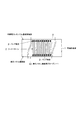
本発明の液晶パネル検査用コンタクトプローブシート10は、図1の一実施形態に示すように、可撓性基板1上に形成されたリードパターン2と、前記リードパターン2における前記表示パネルの各電極に接続する側(表示パネル接続側)に、前記リードパターン2と電気的に接続され、前記表示パネルの各電極に接触するためのバンプ接点3と、を有する。
本発明においては、上記構成1で述べたように、前記バンプ接点の表面が鏡面になっている。
本発明においては、上記構成2で述べたように、各バンプ接点(全てのバンプ接点)の表面の表面粗さ(最大高さ(Rmax))は、0nm超100nm以下とすることが好ましい。
(Embodiment of the Invention)
Hereinafter, modes for carrying out the present invention will be described.
First, the liquid crystal panel inspection contact probe sheet of the present invention will be described.
A
In the present invention, as described in the
In the present invention, as described in the
本発明において、可撓性基板の材料としては、ポリイミド系樹脂、ポリエステル系樹脂、エポキシ系樹脂、ウレタン系樹脂、ポリスチレン系樹脂、ポリエチレン系樹脂、ポリアミド系樹脂、ABS系樹脂、ポリカーポネート系樹脂、シリコーン系樹脂などが挙げられる。可撓性基板の厚さは任意に選択できるが、十分な機械的強度や可撓性を有するようにするため、通常、2μm〜500μmの範囲で設定する。
リードパターン、及びリードパターンとバンプ接点とを接続するための材料としては、導電性を有するものであれば特に限定されないが、公知の良導体金属が好ましい。例えば、銅、金、銀、白金、鉛、錫、ニッケル、鉄、コバルト、インジウム、ロジウム、クロム、タングステン、ルテニウムなどの単体金属、またはこれらを成分とする各種合金、などが挙げられる。
リードパターンを形成する方法としては、可撓性基板の全面に導電性材料層を形成し、目的の回路パターンを残すように他の部分をエッチング等により除去する方法等が挙げられる。
リードパターンとバンプ接点とを連通させ電気的に接続するための可撓性基板に形成されるスルーホールの孔径は限定されないが、隣り合ったスルーホール同士が繋がらない程度まで大きくすることによって、導通部の電気抵抗を小さくできるので好ましい。スルーホールの実用的な孔径は、5μm〜200μmである。表示パネルの検査に使用するコンタクトプローブシートの場合、5μm〜20μmとすることが好ましい。スルーホールの形成方法としては、レーザー加工法、フォトリソグラフィー法、プラズマ加工法、パンチングなどの機械的加工、などの方法が挙げられる。これらの方法の中でも、エキシマレーザー、炭酸ガスレーザー、YAGレーザーなどによるレーザー加工は、スルーホールを任意の孔径や孔間ピッチにて微細加工が可能であり、バンプ接点のファインピッチ化に対応でき、好ましい方法である。
また、リードパターンとバンプ接点とを電気的に接続するため手段としては、スルーホール内に導電性物質を充填してなるもの、スルーホールメッキのように貫通孔の壁面に導電性物質の層を形成してなるものなどがある。形成方法としては、電気メッキ法や無電解メッキ法、CVD法などの成膜方法、機械的に導電性物質をスルーホール内に嵌め込む方法、なとが挙げられる。これらの方法の中でもスルーホール内にリードパターンの一部を構成する材料を露出させ、この材料を負極として電気メッキによってスルーホール内に導電性物質を充填する方法が、確実な導通が得られ、かつ簡便であるので好ましい。
また、バンプ接点の形状は、可撓性基板面からの突出の有無を問わず、接触対象物の形状や材料に応じて、凸状、凹状、平坦パッド状、どのような形状であっても良いが、半球状に突起したものが最も有用である。ここでいう半球状とは完全な半球だけではなく、単調な曲面を持って突起した形状を含む。バンプ接点は複数としても良く、その個数、配置等は限定されない。
In the present invention, the material of the flexible substrate includes polyimide resin, polyester resin, epoxy resin, urethane resin, polystyrene resin, polyethylene resin, polyamide resin, ABS resin, and polycarbonate resin. And silicone resins. The thickness of the flexible substrate can be arbitrarily selected, but is usually set in the range of 2 μm to 500 μm in order to have sufficient mechanical strength and flexibility.
The material for connecting the lead pattern and the lead pattern to the bump contact is not particularly limited as long as it has conductivity, but a known good conductor metal is preferable. Examples thereof include simple metals such as copper, gold, silver, platinum, lead, tin, nickel, iron, cobalt, indium, rhodium, chromium, tungsten, ruthenium, and various alloys containing these as components.
Examples of the method for forming the lead pattern include a method in which a conductive material layer is formed on the entire surface of the flexible substrate, and other portions are removed by etching or the like so as to leave a target circuit pattern.
The hole diameter of the through hole formed in the flexible substrate for connecting and electrically connecting the lead pattern and the bump contact is not limited, but it is made conductive by increasing it to the extent that adjacent through holes are not connected to each other. This is preferable because the electrical resistance of the portion can be reduced. The practical hole diameter of the through hole is 5 μm to 200 μm. In the case of a contact probe sheet used for inspection of a display panel, the thickness is preferably 5 μm to 20 μm. Examples of the through hole forming method include laser processing, photolithography, plasma processing, and mechanical processing such as punching. Among these methods, laser processing with excimer laser, carbon dioxide gas laser, YAG laser, etc. can finely process through holes with any hole diameter and pitch between holes, and can cope with fine pitch of bump contacts, This is the preferred method.
In addition, as means for electrically connecting the lead pattern and the bump contact, the through hole is filled with a conductive material, and a layer of a conductive material is formed on the wall surface of the through hole like through-hole plating. Some are formed. Examples of the forming method include a film forming method such as an electroplating method, an electroless plating method, and a CVD method, and a method of mechanically fitting a conductive substance into the through hole. Among these methods, a method of exposing a material constituting a part of the lead pattern in the through hole and filling the through hole with a conductive substance by electroplating using this material as a negative electrode provides reliable conduction, And it is preferable because it is simple.
In addition, the shape of the bump contact may be any shape such as a convex shape, a concave shape, a flat pad shape, depending on the shape and material of the contact object, regardless of whether or not it protrudes from the surface of the flexible substrate. Although good, a hemispherical protrusion is most useful. Here, the hemispherical shape includes not only a perfect hemisphere but also a protruding shape having a monotonous curved surface. There may be a plurality of bump contacts, and the number, arrangement, etc. thereof are not limited.
本発明においては、上記構成3で述べたように、バンプ接点を、金属と炭素を含む材料で構成することにより、バンプ接点を構成する結晶の粒径が小さくなることで、バンプ接点表面の表面粗さを小さくすることができる。これに加え、各金属結晶の粒界に炭素が集中することで硬度が高くなるか、または、金属の結晶の間に硬度が高い金属の炭化物が入りこみバンプ接点全体として硬度が高くなるので、コンタクトプローブシートの寿命が飛躍的に向上する。
バンプ接点中に炭素を含有させる方法としては、メッキ溶液中にメッキ溶液に溶解する有機物質を入れ、メッキ条件を調整することによってできる。メッキ溶液中にいれる有機物質としては、メッキ溶液に溶解する有機物質であって、バンプ接点を電気メッキ法等で製造する際に、バンプ接点に炭素が取り込まれる作用を有する有機物質であれば良い。例えば、炭酸(H2CO3)、二酸化炭素(CO2)、サンカリン、ショ糖、ブドウ糖などであっても良い。
In the present invention, as described in the
As a method for containing carbon in the bump contact, an organic substance that dissolves in the plating solution is placed in the plating solution, and the plating conditions are adjusted. The organic substance contained in the plating solution may be an organic substance that dissolves in the plating solution and has an action of incorporating carbon into the bump contact when the bump contact is manufactured by an electroplating method or the like. . For example, carbonic acid (H 2 CO 3 ), carbon dioxide (CO 2 ), sankaline, sucrose, glucose and the like may be used.
本発明においては、上記構成4で述べたように、バンプ接点表面に、金メッキを形成することによって、金メッキはNi等からなるコアバンプと比べ柔らかい材料であること、金メッキによってバンプ接点表面の表面粗さが若干粗れていてもITO電極にダメージと見なされる損傷を与える恐れが少ないことから、柔らかい金メッキによるバンプ接点表面の表面粗さの若干の粗れ、即ち金の電気伝導性(電気的接触性)及び柔らかい金メッキ表面の表面粗さの適度な粗れの相乗作用によって、1バンプ接点当たりの加重を従来の1/2〜1/3の加重で接触させたても、全電極の電気的コンタクトを確保でき、しかもITO又はIZO等の電極にダメージと見なされる損傷を与えることがない。
金メッキの条件、厚さ、表面粗さ等は、上記作用効果が効果的に得られるように調整する。
In the present invention, as described in the
The conditions, thickness, surface roughness, etc. of the gold plating are adjusted so that the above effects can be obtained effectively.
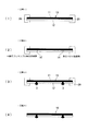
次に、本発明の表示パネル検査用コンタクトプローブシートの製造方法について、図2を参照して説明する。
(工程1):まず、銅箔11とポリイミドフィルム12とを積層した構造のフィルム13を張力が均一に係った状態で固定治具20に固定する(図2(1))。
(工程2):次に、銅箔11を周知のリソグラフィー法でエッチングしてリードパターンを形成した後、液晶パネルの電極と接続する側に表示パネルの電極のピッチと同じピッチ(約40μm)でエキシマレーザーにより、ポリイミドフィルム12に直径約10μmのスルーホール14を形成する。
また、液晶パネルの電極と接続する側とは反対側である、中継用フレキシブル基板と接続する側に、中継用フレキシブル基板の配線パターンと同じピッチ(約80μm)でエキシマレーザーによりポリイミドフィルムに直径約10μmのスルーホール14’を形成する(図2(2))。
(工程3):次に、表面側の銅箔面(リードパターン側の面)がメッキされないように保護した後、銅箔11(各リードパターン)の一部にそれぞれメッキ用電極を持続し、スルーホール内に露出した銅箔を負極として、ニッケルと炭素を含むニッケル合金の電気メッキを行う。
ニッケル合金をスルーホール内に析出させて充填し、さらに析出を継続して、ポリイミド面12’から約10μm突出した高さまで半球状に成長させて、バンプ接点3を形成した(図2(3))。尚、電気メッキの際に、メッキ液へ強度増強剤及び応力緩和剤を添加するとともに、メッキ条件並びに硬度増強剤及び応力緩和剤の量を調整することによって、バンプ接点3を構成する材料の結晶粒径を制御して、バンプ接点3表面の表面粗さを制御(鏡面化)した。
(工程4):最後に、固定治具20から積層構造フィルム13を外して液晶パネル検査用コンタクトプローブシート10を作製する(図2(4))。
Next, the manufacturing method of the contact probe sheet | seat for a display panel test | inspection of this invention is demonstrated with reference to FIG.
(Step 1): First, the
(Step 2): Next, after the
Also, on the side connected to the flexible substrate for relay, which is opposite to the side connected to the electrode of the liquid crystal panel, the diameter of the polyimide film is approximately the same as the wiring pattern of the flexible substrate for relay (about 80 μm) by excimer laser. A 10 μm through
(Step 3): Next, after protecting the copper foil surface on the surface side (surface on the lead pattern side) from being plated, the plating electrode is maintained on a part of the copper foil 11 (each lead pattern), Electroplating of a nickel alloy containing nickel and carbon is performed using the copper foil exposed in the through hole as a negative electrode.
The nickel alloy was deposited and filled in the through hole, and further the deposition was continued to grow hemispherically to a height protruding about 10 μm from the
(Step 4): Finally, the
次に、本発明の液晶パネル検査用コンタクトプローブユニットについて説明する。
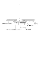
本発明の液晶パネル検査用コンタクトプローブユニットは、図3の一実施形態に示すように、表示パネル検査用コンタクトプローブシート10と、前記コンタクトプローブシート10における少なくとも前記表示パネルの各電極に接続する側を載置し支持するための支持台(シートを固定させる筐体)30と、を有する。
支持台おける少なくとも前記表示パネルの各電極に接続する側を載置し支持する面は、平坦(好ましくは±5μm程度)とすることが好ましい。支持台の材質はアルミニウム、SUSなどが好ましい。
表示パネル検査用コンタクトプローブシート10と支持台30との間には、弾性シート(好ましくはシリコンゴムシート)40を介在させることが好ましい。弾性シートとプローブシートとの間は接着する必要はなくプローブシートの交換が容易である。
表示パネル検査用コンタクトプローブシートを、支持台上の所定位置に位置決め固定するためには、例えば、支持台上の所定位置に位置決め用のピンを設け、このピンに表示パネル検査用コンタクトプローブシートに設けた穴を通す手段が簡便でありしかも高位置精度が実現できる。プローブシートの交換も容易である。
また、表示パネル検査用コンタクトプローブシート及び支持台に、それぞれアライメントマークを設け、表示パネル検査用コンタクトプローブシートを、支持台上の所定位置に位置決め固定することもできる。
表示パネル検査用コンタクトプローブシート及び支持台には、それぞれ、表示パネル側のアライメントマークと位置あわせするためのアライメントマークを設けることができる。
支持台は、昇降機構及び加圧機構等で駆動することによって、表示パネルの検査を行う。
本発明の液晶パネル検査用コンタクトプローブユニットは、前記支持台に載置された前記コンタクトプローブシートを狭持し固定するための抑え具、を有することが好ましい。
これは、前記支持台に載置されたコンタクトプローブシートを抑え具により上方から狭持することによって、繰り返しコンタクトさせた場合であってもコンタクトプローブシートに位置ずれ等を生じさせず、確実且つ安定的な表示パネル検査用コンタクトプローブユニットを提供できるからである。
上記構成によれば、表示パネルの電極にダメージを発生させない表示パネル検査用コンタクトプローブシートを具備した表示パネル検査用コンタクトプローブユニットであって繰り返しコンタクトさせた場合であってもコンタクトプローブシートに位置ずれ等を生じさせず、確実且つ安定的な表示パネル検査用コンタクトプローブユニットを提供できる。
Next, the liquid crystal panel inspection contact probe unit of the present invention will be described.
As shown in one embodiment of FIG. 3, the liquid crystal panel inspection contact probe unit of the present invention includes a display panel inspection
It is preferable that the surface of the support base on which at least the side connected to each electrode of the display panel is placed and supported is flat (preferably about ± 5 μm). The material of the support base is preferably aluminum or SUS.
An elastic sheet (preferably a silicon rubber sheet) 40 is preferably interposed between the display panel inspection
In order to position and fix the display panel inspection contact probe sheet at a predetermined position on the support base, for example, a positioning pin is provided at a predetermined position on the support base, and this pin is used as a contact probe sheet for display panel inspection. The provided means for passing the holes is simple and high position accuracy can be realized. The probe sheet can be easily replaced.
In addition, alignment marks can be provided on the display panel inspection contact probe sheet and the support base, respectively, and the display panel inspection contact probe sheet can be positioned and fixed at a predetermined position on the support base.
Each of the display panel inspection contact probe sheet and the support base may be provided with an alignment mark for alignment with the alignment mark on the display panel side.
The support base inspects the display panel by being driven by an elevating mechanism and a pressurizing mechanism.
The contact probe unit for inspecting a liquid crystal panel of the present invention preferably has a pressing member for sandwiching and fixing the contact probe sheet placed on the support base.
This is because the contact probe sheet placed on the support base is sandwiched from above by a holding tool so that the contact probe sheet is not misaligned even if it is repeatedly contacted, and it is reliable and stable. This is because a typical contact probe unit for display panel inspection can be provided.
According to the above configuration, even if the contact probe unit for display panel inspection is provided with the contact probe sheet for display panel inspection that does not cause damage to the electrodes of the display panel and is repeatedly contacted, it is displaced from the contact probe sheet. Thus, it is possible to provide a reliable and stable contact probe unit for inspecting a display panel without causing the above.
次に、本発明の実施例について説明する。
(実施例1)
上述の液晶パネル検査用コンタクトプローブシートの製造方法により、ポリイミドフィルムと鋼箔とを積層した構造の2層フィルム(ポリイミド膜厚12.5μm、鋼箔厚5μm)を用い、銅からなるリードパターンのピッチが約40μm、リードパターンの表面に形成されたニッケルと炭素とを含むバンプ接点のバンプ径(直径)が約30μm、高さが約10μmの液晶パネル検査用コンタクトプローブシートを作製した。形成されたバンプ接点の表面を顕微鏡で観察したところ鏡面で、バンプ接点表面の表面粗さを原子間力顕微鏡(AFM)にて測定(測定エリア2μm□、この測定エリアはITO電極と接触するバンプ接点頂部の領域に略相当する)したところ、最大高さ(Rmax)は13nm〜18nm、平均粗さ(Ra)は1.2nmであった。なお、最大高さ(Rmax)及び算術平均粗さ(Ra)は、それぞれ日本工業規格JISB0601の最大高さRmax及び算術平均粗さRaに準拠して算出した。
上記で得られたコンタクトプローブシートをコンタクトプローブユニットを介して液晶パネル検査装置に装着し、有機ELパネルの検査を1バンプ接点あたり2g及び4gの加重で10万回行った後、顕微鏡(倍率500倍)でバンプ接点表面及びITO電極の観察を行ったところ、バンプ接点表面にダメージは観察されず、また、有機ELパネルに形成された被検査対象であるITO電極にもダメージと見なされる窪みや、ダメージと見なされる傷、クラック(ひび)、断線等の損傷は観察されなかった。また、パネル点灯試験、パネル特性試験を支障なく行うことができた。
Next, examples of the present invention will be described.
(Example 1)
Using the above-described method for manufacturing a contact probe sheet for inspecting a liquid crystal panel, a two-layer film (polyimide film thickness 12.5 μm, steel foil thickness 5 μm) having a structure in which a polyimide film and a steel foil are laminated is used. A contact probe sheet for inspecting a liquid crystal panel having a pitch of about 40 μm, a bump diameter (diameter) of a bump contact including nickel and carbon formed on the surface of the lead pattern of about 30 μm and a height of about 10 μm was produced. When the surface of the formed bump contact was observed with a microscope, the surface of the bump contact was measured with a mirror surface, and the surface roughness of the bump contact surface was measured with an atomic force microscope (AFM) (
The contact probe sheet obtained above is mounted on a liquid crystal panel inspection apparatus through a contact probe unit, and the organic EL panel is inspected 100,000 times with a load of 2 g and 4 g per bump contact, and then a microscope (magnification 500) When the surface of the bump contact and the ITO electrode are observed, no damage is observed on the surface of the bump contact, and the ITO electrode that is the object of inspection formed on the organic EL panel is considered to be damaged. Damages such as scratches, cracks, and disconnections considered as damage were not observed. Moreover, the panel lighting test and the panel characteristic test could be performed without any trouble.
なお、ニッケルは、ニッケルと炭素とを含むバンプ接点は、硬度が高いため、ITO電極にダメージと見なされる損傷を与えるリスクをより以上に少なくするためには、より高い平滑性が必要であり、バンプ接点表面の表面粗さは、最大高さ(Rmax)で20nm以下とすることが好ましく、10nm以下とすることが更に好ましい。 In addition, since the bump contact containing nickel and carbon has high hardness, in order to further reduce the risk of damaging the ITO electrode as damage, higher smoothness is required. The surface roughness of the bump contact surface is preferably 20 nm or less, more preferably 10 nm or less in terms of the maximum height (Rmax).
(実施例2)
実施例1のバンプ接点表面に、厚さ0.1nm〜0.2nmの金メッキを形成した以外は実施例1と同様にして液晶パネル検査用コンタクトプローブシートを作製した。形成されたバンプ接点の表面を顕微鏡で観察したところ鏡面で、バンプ接点表面の表面粗さを原子間力顕微鏡にて測定(測定エリア2μm□、この測定エリアはITO電極と接触するバンプ接点頂部の領域に略相当する)したところ、最大高さ(Rmax)は55nm〜73nm、平均粗さ(Ra)は5.4であった。なお、最大高さ(Rmax)及び算術平均粗さ(Ra)は、それぞれ日本工業規格JISB0601の最大高さRmax及び算術平均粗さRaに準拠して算出した。
上記で得られたコンタクトプローブシートをコンタクトプローブユニットを介して液晶パネル検査装置に装着し、有機ELパネルの検査を1バンプ接点あたり2g及び4gの加重で10万回行った後、顕微鏡(倍率500倍)でバンプ接点表面及びITO電極の観察を行ったところ、バンプ接点表面にダメージは観察されず、また、有機ELパネルに形成された被検査対象であるITO電極にもダメージと見なされる窪みや、ダメージと見なされる傷、クラック(ひび)、断線等の損傷は観察されなず、更にITO電極におけるバンプ接点の接触痕は実施例1に比べ軽減されていた。また、パネル点灯試験、パネル特性試験を支障なく行うことができた。
(Example 2)
A contact probe sheet for inspecting a liquid crystal panel was produced in the same manner as in Example 1 except that gold plating having a thickness of 0.1 nm to 0.2 nm was formed on the bump contact surface of Example 1. When the surface of the formed bump contact was observed with a microscope, the surface of the bump contact was measured with a mirror surface, and the surface roughness of the bump contact surface was measured with an atomic force microscope (
The contact probe sheet obtained above is mounted on a liquid crystal panel inspection apparatus through a contact probe unit, and the organic EL panel is inspected 100,000 times with a load of 2 g and 4 g per bump contact, and then a microscope (magnification 500) When the surface of the bump contact and the ITO electrode are observed, no damage is observed on the surface of the bump contact, and the ITO electrode that is the object of inspection formed on the organic EL panel is considered to be damaged. No damage such as scratches, cracks, breaks, etc., that were regarded as damage was observed, and the contact traces of the bump contacts on the ITO electrode were reduced as compared with Example 1. Moreover, the panel lighting test and the panel characteristic test could be performed without any trouble.
金メッキは、メッキ法で形成したNiバンプ接点と比べ柔らかい材料なので、金メッキによってバンプ接点表面の表面粗さが若干粗れていてもITO電極にダメージと見なされる損傷を与える恐れが少なく、しかも柔らかい金メッキによるバンプ接点表面の表面粗さの若干の粗れ、即ち金の電気伝導性(電気的接触性)及び柔らかい金メッキ表面の表面粗さの適度な粗れ(Rmaxで50nm〜80nm)の相乗作用によって、1バンプ接点当たり加重2g及び4gで接触させたても、全電極の電気的コンタクトを確保でき、しかもITO又はIZO電極にダメージと見なされる損傷を与えることがない。 Gold plating is a soft material compared to Ni bump contacts formed by plating, so even if the surface roughness of the bump contacts is slightly rough due to gold plating, there is little risk of damaging the ITO electrode and it is soft gold plating Due to the synergistic effect of the surface roughness of the bump contact surface due to a slight roughness, that is, the electrical conductivity of gold (electrical contact) and the moderate roughness of the surface roughness of the soft gold-plated surface (Rmax 50 nm to 80 nm) Even if contact is applied at a weight of 2 g and 4 g per bump contact, electrical contact of all the electrodes can be ensured, and the ITO or IZO electrode is not considered to be damaged.
(比較例)
実施例1又は実施例2のバンプ接点の材料をニッケル単体とした以外は実施例1と同様にして液晶パネル検査用コンタクトプローブシートを作製した。形成されたバンプ接点の表面を顕微鏡で観察したところ表面は荒れており粗面で、バンプ接点表面の表面粗さを原子間力顕微鏡にて測定(測定エリア2μm□、この測定エリアはITO電極と接触するバンプ接点頂部の領域に略相当する)したところ、最大高さ(Rmax)は124nm〜183であった。なお、最大高さ(Rmax)及び算術平均粗さ(Ra)は、それぞれ日本工業規格JISB0601の最大高さRmax及び算術平均粗さRaに準拠して算出した。
上記で得られたコンタクトプローブシートをコンタクトプローブユニットを介して液晶パネル検査装置に装着し、有機ELパネルの検査を1バンプ接点あたり2g及び4gの加重で10万回行った。その結果、金メッキの有無にかかわらず、有機ELパネルの電極と接触していたバンプ接点表面は荒れており、表面の凹部にITO膜片が見つかり、また、被検査対象である有機ELパネルに形成された電極にもダメージと見なされる窪み(深い窪みとその周縁の盛り上がりを有しドライバIC等の搭載の障害となる窪み)や、ダメージと見なされる傷、クラック(ひび)、断線等の損傷が発生していた。そのため、パネル点灯試験、パネル特性試験に支障を生じた。
(Comparative example)
A contact probe sheet for inspecting a liquid crystal panel was produced in the same manner as in Example 1 except that the material of the bump contact in Example 1 or Example 2 was nickel alone. When the surface of the formed bump contact was observed with a microscope, the surface was rough and rough, and the surface roughness of the bump contact surface was measured with an atomic force microscope (
The contact probe sheet obtained above was mounted on a liquid crystal panel inspection apparatus via a contact probe unit, and the organic EL panel was inspected 100,000 times with a weight of 2 g and 4 g per bump contact. As a result, regardless of the presence or absence of gold plating, the bump contact surface that was in contact with the electrode of the organic EL panel was rough, and an ITO film piece was found in the concave portion of the surface, and formed on the organic EL panel to be inspected There are also pits that are regarded as damage (deep pits and bulges around the periphery of the electrodes, which are obstacles to the mounting of driver ICs, etc.), and damage such as scratches, cracks, and disconnections that are considered as damage. It has occurred. This hindered the panel lighting test and panel characteristic test.
以上の実施例及び比較例の結果から、液晶パネルの電極にダメージと見なされる窪み(深い窪みとその周縁の盛り上がりを有しドライバIC等の搭載の障害となる窪み)や、傷、クラック(ひび)、断線等の損傷を発生させないためには、上述の実施例のような表面が鏡面のバンプ接点を有するコンタクトプローブシートが必要不可欠であることがわかった。 From the results of the above-described examples and comparative examples, a recess (a recess having a deep recess and a bulge at the periphery thereof, which hinders mounting of a driver IC or the like), scratch, crack (crack) In order to prevent damage such as disconnection, it has been found that a contact probe sheet having a bump contact with a mirror surface as in the above-described embodiment is indispensable.
実施例1,2及び比較例における、バンプ接点部の結晶粒径は10nm以上40nm以下、バンプ接点中の炭素含有量(ニッケルの炭化物として含有される炭素の量)は0.2at%〜1.2at%、バンプ接点部の硬度は450Hv以上950Hv以下、であった。また、比較例1における、バンプ接点部の結晶粒径は50nm以上、バンプ接点中の炭素含有量(ニッケルの炭化物として含有される炭素の量)は0at%、バンプ接点部の硬度は220Hv(十分な硬度が得られない)、であった。
なお、バンプ接点部の結晶粒径は、X線ディフラクトメータにより平均粒子経を測定した。バンプ接点中の炭素の量は、X線光電子分光法(XPS:X-ray Photoelectro Spectroscopy)にて測定した。同様に、金属炭化物の存在は、XPSにて確認した。バンプ接点部の硬度は、銅板の上に膜厚30μm以上にメッキし、マイクロビッカース硬度計で測定した。なお、 実施例1,2のバンプ接点をESCAで分析したところ、各バンプ接点には、ニッケルの炭化物がニッケルカーバイドの形で形成されていることが確認された。
In Examples 1 and 2 and the comparative example, the crystal grain size of the bump contact portion is 10 nm or more and 40 nm or less, and the carbon content in the bump contact (amount of carbon contained as nickel carbide) is 0.2 at% to 1. The hardness of the bump contact part was 2 at% and 450 Hv or more and 950 Hv or less. In Comparative Example 1, the bump contact portion has a crystal grain size of 50 nm or more, the carbon content in the bump contact (the amount of carbon contained as nickel carbide) is 0 at%, and the bump contact portion has a hardness of 220 Hv (sufficiently) A high hardness cannot be obtained).
The crystal grain size of the bump contact portion was measured by an average particle size using an X-ray diffractometer. The amount of carbon in the bump contact was measured by X-ray photoelectron spectroscopy (XPS). Similarly, the presence of metal carbide was confirmed by XPS. The hardness of the bump contact part was plated on a copper plate to a film thickness of 30 μm or more and measured with a micro Vickers hardness meter. When the bump contacts in Examples 1 and 2 were analyzed by ESCA, it was confirmed that nickel carbide was formed in the form of nickel carbide on each bump contact.
なお、ニッケルと炭素とを含むバンプ接点においては、炭素の含有量が少なすぎる場合は、十分な硬度が得られず、また、炭素が多すぎる場合は、応力が高くなりすぎるとともに、バンプ接点にクラックなどの欠陥が発生しやすくなり、バンプ接点が脱離しやすくなる。
また、ニッケルと炭素とを含むバンプ接点においては、結晶粒径が小さくなるに従い、硬度が高くなる。結晶粒径が大きすぎる場合、十分な硬度が得られず、バンプ接点が脱離しやすい。結晶粒径が小さすぎる場合、硬度が上がりすぎ、バンプ接点にクラック等の欠陥が発生しやすく、バンプ接点の応力が高くなり、バンプ接点が脱離しやすい。
なお、バンプ接点の硬度を高くしすぎると、バンプ接点にクラックが生じ易くなり、可撓性基板からバンプ接点が破損しやすくなるという相反する問題がある。また、バンプ接点の硬度を高くしすぎると、形成されたバンプ接点が、バンプ接点形成時や繰り返し加圧接触の際に、脱離しやすい。
本発明によれば、プローブ接点の結晶粒経やプローブ接点中に含まれる炭素の量を調整することで、プローブ接点の、表面粗さ、硬度及び脱離耐性等をコントロールすることが可能なる。従って、本願発明の課題解決に適したバンプ接点の表面粗さを有しかつ耐久性に優れたプローブ接点を有する表示パネル検査用コンタクトプローブシートが得られる。
In bump contacts containing nickel and carbon, if the carbon content is too low, sufficient hardness cannot be obtained, and if there is too much carbon, the stress becomes too high and the bump contact Defects such as cracks are likely to occur, and the bump contacts are easily detached.
Moreover, in the bump contact containing nickel and carbon, the hardness increases as the crystal grain size decreases. If the crystal grain size is too large, sufficient hardness cannot be obtained, and the bump contacts are easily detached. When the crystal grain size is too small, the hardness is excessively increased, and defects such as cracks are likely to occur in the bump contact, the stress of the bump contact is increased, and the bump contact is easily detached.
If the hardness of the bump contact is excessively high, cracks are likely to occur in the bump contact, and there is a conflicting problem that the bump contact is easily damaged from the flexible substrate. Further, if the hardness of the bump contact is too high, the formed bump contact tends to be detached when the bump contact is formed or repeatedly pressed.
According to the present invention, it is possible to control the surface roughness, hardness, desorption resistance, and the like of the probe contact by adjusting the crystal grain size of the probe contact and the amount of carbon contained in the probe contact. Therefore, a display panel inspection contact probe sheet having a bump contact surface roughness suitable for solving the problems of the present invention and having a probe contact excellent in durability can be obtained.
1 可撓性基板
2 リードパターン
3 バンプ接点
10 表示パネル検査用コンタクトプローブシート
30 支持台
40 弾性シート
DESCRIPTION OF
Claims (6)
前記コンタクトプローブシートは、可撓性基板上に形成されたリードパターンと、
前記リードパターンにおける前記表示パネルの各電極に接続する側に、前記リードパターンと電気的に接続された、前記表示パネルの各電極に接触するためのバンプ接点と、を有し、
前記バンプ接点の表面は、鏡面であることを特徴とする表示パネル検査用コンタクトプローブシート。 A contact probe sheet for inspecting a display panel used for conducting a predetermined test by energizing each electrode of the display panel,
The contact probe sheet includes a lead pattern formed on a flexible substrate;
A bump contact for contacting each electrode of the display panel, electrically connected to the lead pattern, on a side connected to each electrode of the display panel in the lead pattern,
A contact probe sheet for inspecting a display panel, wherein a surface of the bump contact is a mirror surface.
Priority Applications (1)
| Application Number | Priority Date | Filing Date | Title |
|---|---|---|---|
| JP2004106986A JP4246097B2 (en) | 2004-03-31 | 2004-03-31 | Display probe inspection contact probe sheet and display panel inspection contact probe unit equipped with the display panel inspection contact probe sheet |
Applications Claiming Priority (1)
| Application Number | Priority Date | Filing Date | Title |
|---|---|---|---|
| JP2004106986A JP4246097B2 (en) | 2004-03-31 | 2004-03-31 | Display probe inspection contact probe sheet and display panel inspection contact probe unit equipped with the display panel inspection contact probe sheet |
Publications (2)
| Publication Number | Publication Date |
|---|---|
| JP2005291912A true JP2005291912A (en) | 2005-10-20 |
| JP4246097B2 JP4246097B2 (en) | 2009-04-02 |
Family
ID=35325000
Family Applications (1)
| Application Number | Title | Priority Date | Filing Date |
|---|---|---|---|
| JP2004106986A Expired - Fee Related JP4246097B2 (en) | 2004-03-31 | 2004-03-31 | Display probe inspection contact probe sheet and display panel inspection contact probe unit equipped with the display panel inspection contact probe sheet |
Country Status (1)
| Country | Link |
|---|---|
| JP (1) | JP4246097B2 (en) |
Cited By (6)
| Publication number | Priority date | Publication date | Assignee | Title |
|---|---|---|---|---|
| JP2007024613A (en) * | 2005-07-14 | 2007-02-01 | Genesis Technology Inc | Contact terminal and connector for semiconductor device inspection using the same |
| JP2007157620A (en) * | 2005-12-08 | 2007-06-21 | D D K Ltd | Electrical contact structure |
| US8509036B2 (en) | 2010-12-09 | 2013-08-13 | Tdk Corporation | Method of burn-in testing for thermally assisted head |
| US8957692B2 (en) | 2010-12-02 | 2015-02-17 | Tdk Corporation | Method for performing burn-in test |
| CN110974140A (en) * | 2019-12-24 | 2020-04-10 | 苏州佳世达光电有限公司 | Oral scanner, reflector device for ensuring flatness of reflector and assembling method |
| JP2023110479A (en) * | 2022-01-28 | 2023-08-09 | 三菱電機株式会社 | Electrical characteristic test equipment and jig storage |
-
2004
- 2004-03-31 JP JP2004106986A patent/JP4246097B2/en not_active Expired - Fee Related
Cited By (7)
| Publication number | Priority date | Publication date | Assignee | Title |
|---|---|---|---|---|
| JP2007024613A (en) * | 2005-07-14 | 2007-02-01 | Genesis Technology Inc | Contact terminal and connector for semiconductor device inspection using the same |
| JP2007157620A (en) * | 2005-12-08 | 2007-06-21 | D D K Ltd | Electrical contact structure |
| US8957692B2 (en) | 2010-12-02 | 2015-02-17 | Tdk Corporation | Method for performing burn-in test |
| US8509036B2 (en) | 2010-12-09 | 2013-08-13 | Tdk Corporation | Method of burn-in testing for thermally assisted head |
| CN110974140A (en) * | 2019-12-24 | 2020-04-10 | 苏州佳世达光电有限公司 | Oral scanner, reflector device for ensuring flatness of reflector and assembling method |
| JP2023110479A (en) * | 2022-01-28 | 2023-08-09 | 三菱電機株式会社 | Electrical characteristic test equipment and jig storage |
| JP7580417B2 (en) | 2022-01-28 | 2024-11-11 | 三菱電機株式会社 | Electrical Property Test Equipment |
Also Published As
| Publication number | Publication date |
|---|---|
| JP4246097B2 (en) | 2009-04-02 |
Similar Documents
| Publication | Publication Date | Title |
|---|---|---|
| KR100801395B1 (en) | Manufacturing method of probe sheet | |
| US5748179A (en) | LCD device having driving circuits with multilayer external terminals | |
| JP2010145731A (en) | Display device | |
| JP2010276541A (en) | Thin film probe sheet and manufacturing method thereof, probe card, and semiconductor chip inspection apparatus | |
| JP4246097B2 (en) | Display probe inspection contact probe sheet and display panel inspection contact probe unit equipped with the display panel inspection contact probe sheet | |
| KR100947608B1 (en) | Flexible film | |
| US7893533B2 (en) | Semiconductor device, mounting structure, electro-optical apparatus, electronic system, and method for manufacturing electronic component | |
| KR20060128685A (en) | Manufacturing method of semiconductor integrated circuit device | |
| JP4246096B2 (en) | Display probe inspection contact probe sheet and display panel inspection contact probe unit equipped with the display panel inspection contact probe sheet | |
| JPH06249880A (en) | Probe unit | |
| KR100896439B1 (en) | Flexible film | |
| JP4479512B2 (en) | Circuit board member and method of manufacturing circuit board member | |
| KR20050075641A (en) | A flexible printed circuit board | |
| JP2005291919A (en) | Display probe inspection contact probe sheet and display panel inspection contact probe unit equipped with the display panel inspection contact probe sheet | |
| CN114815422B (en) | Display panel and manufacturing method thereof | |
| CN207440454U (en) | A kind of glass positioning device for glass for the assembling of mobile phone liquid crystal display panel | |
| JP2007271343A (en) | Contact probe and manufacturing method thereof | |
| KR102936595B1 (en) | Improved multilayer contact film, and manufacturing method applied to the same | |
| JP4204919B2 (en) | Contact component, method for manufacturing the same, and inspection jig having the contact component | |
| CN113299604A (en) | Manufacturing method of backboard, display panel and display device | |
| JP2005016959A (en) | Display panel inspection device | |
| CN213302711U (en) | Display panel lighting detection device | |
| CN115061300B (en) | Display panel, manufacturing method of display panel and display device | |
| JP5320309B2 (en) | Probe card | |
| JPH1164381A (en) | Contact probe, method of manufacturing the same, and probe device provided with the contact probe |
Legal Events
| Date | Code | Title | Description |
|---|---|---|---|
| A621 | Written request for application examination |
Free format text: JAPANESE INTERMEDIATE CODE: A621 Effective date: 20070323 |
|
| A977 | Report on retrieval |
Free format text: JAPANESE INTERMEDIATE CODE: A971007 Effective date: 20080904 |
|
| A131 | Notification of reasons for refusal |
Free format text: JAPANESE INTERMEDIATE CODE: A131 Effective date: 20080930 |
|
| A521 | Request for written amendment filed |
Free format text: JAPANESE INTERMEDIATE CODE: A523 Effective date: 20081125 |
|
| TRDD | Decision of grant or rejection written | ||
| A01 | Written decision to grant a patent or to grant a registration (utility model) |
Free format text: JAPANESE INTERMEDIATE CODE: A01 Effective date: 20090106 |
|
| A01 | Written decision to grant a patent or to grant a registration (utility model) |
Free format text: JAPANESE INTERMEDIATE CODE: A01 |
|
| A61 | First payment of annual fees (during grant procedure) |
Free format text: JAPANESE INTERMEDIATE CODE: A61 Effective date: 20090107 |
|
| R150 | Certificate of patent or registration of utility model |
Free format text: JAPANESE INTERMEDIATE CODE: R150 |
|
| FPAY | Renewal fee payment (event date is renewal date of database) |
Free format text: PAYMENT UNTIL: 20120116 Year of fee payment: 3 |
|
| FPAY | Renewal fee payment (event date is renewal date of database) |
Free format text: PAYMENT UNTIL: 20120116 Year of fee payment: 3 |
|
| FPAY | Renewal fee payment (event date is renewal date of database) |
Free format text: PAYMENT UNTIL: 20130116 Year of fee payment: 4 |
|
| FPAY | Renewal fee payment (event date is renewal date of database) |
Free format text: PAYMENT UNTIL: 20130116 Year of fee payment: 4 |
|
| FPAY | Renewal fee payment (event date is renewal date of database) |
Free format text: PAYMENT UNTIL: 20140116 Year of fee payment: 5 |
|
| R250 | Receipt of annual fees |
Free format text: JAPANESE INTERMEDIATE CODE: R250 |
|
| LAPS | Cancellation because of no payment of annual fees |