JP2005291847A - IC evaluation jig - Google Patents
IC evaluation jig Download PDFInfo
- Publication number
- JP2005291847A JP2005291847A JP2004105543A JP2004105543A JP2005291847A JP 2005291847 A JP2005291847 A JP 2005291847A JP 2004105543 A JP2004105543 A JP 2004105543A JP 2004105543 A JP2004105543 A JP 2004105543A JP 2005291847 A JP2005291847 A JP 2005291847A
- Authority
- JP
- Japan
- Prior art keywords
- lead
- measured
- high frequency
- pressing
- wiring board
- Prior art date
- Legal status (The legal status is an assumption and is not a legal conclusion. Google has not performed a legal analysis and makes no representation as to the accuracy of the status listed.)
- Pending
Links
- 238000011156 evaluation Methods 0.000 title claims abstract description 28
- 238000003825 pressing Methods 0.000 claims abstract description 61
- 229920005989 resin Polymers 0.000 claims abstract description 10
- 239000011347 resin Substances 0.000 claims abstract description 10
- 238000012360 testing method Methods 0.000 claims abstract description 4
- 230000000149 penetrating effect Effects 0.000 claims abstract description 3
- 230000017525 heat dissipation Effects 0.000 abstract description 9
- 238000000465 moulding Methods 0.000 abstract description 2
- 230000005855 radiation Effects 0.000 abstract description 2
- 238000005259 measurement Methods 0.000 description 7
- 239000000758 substrate Substances 0.000 description 7
- 229910052751 metal Inorganic materials 0.000 description 5
- 239000002184 metal Substances 0.000 description 5
- 238000000034 method Methods 0.000 description 5
- 239000004065 semiconductor Substances 0.000 description 5
- 238000010586 diagram Methods 0.000 description 4
- 238000007689 inspection Methods 0.000 description 4
- 239000000463 material Substances 0.000 description 4
- 230000005489 elastic deformation Effects 0.000 description 3
- 239000013013 elastic material Substances 0.000 description 2
- 239000012778 molding material Substances 0.000 description 2
- 239000002893 slag Substances 0.000 description 2
- 241000272168 Laridae Species 0.000 description 1
- 229910052782 aluminium Inorganic materials 0.000 description 1
- XAGFODPZIPBFFR-UHFFFAOYSA-N aluminium Chemical compound [Al] XAGFODPZIPBFFR-UHFFFAOYSA-N 0.000 description 1
- 238000013459 approach Methods 0.000 description 1
- 230000005540 biological transmission Effects 0.000 description 1
- 230000015572 biosynthetic process Effects 0.000 description 1
- 239000003990 capacitor Substances 0.000 description 1
- 230000000694 effects Effects 0.000 description 1
- 239000000835 fiber Substances 0.000 description 1
- 238000004806 packaging method and process Methods 0.000 description 1
- 238000007789 sealing Methods 0.000 description 1
- 229920003002 synthetic resin Polymers 0.000 description 1
- 239000000057 synthetic resin Substances 0.000 description 1
Images
Landscapes
- Testing Of Individual Semiconductor Devices (AREA)
Abstract
Description
本発明は、パッケージされたICを測定・検査する評価治具に関し、IC押さえ部材に収納させて評価用の配線基板上に載置固定するIC評価治具に関する。 The present invention relates to an evaluation jig that measures and inspects a packaged IC, and relates to an IC evaluation jig that is housed in an IC pressing member and placed and fixed on an evaluation wiring board.
樹脂によるパッケージが完了したICは、その出荷前に電気的特性が測定・検査される。電気的特性には、DC的なものとAC的なダイナミック特性とがある。ICの動作帯域が数十〜数百MHz程度で使用される場合は、AC特性を測定する際に問題にならなかったようなことでも、動作帯域が数百MHzを越えGHz帯に近づくと、伝送インピーダンスの影響が顕著に現れてくる。このような高周波帯域では、ICへの入出力でインピーダンス不整合があると、ICへの入力信号及びICからの出力信号波形に歪が生じ、正確なAC特性の評価ができなくなる。 An IC whose packaging with resin is completed is measured and inspected for electrical characteristics before shipment. The electrical characteristics include DC characteristics and AC dynamic characteristics. When the operating band of the IC is used in the order of several tens to several hundreds of MHz, even if there is no problem when measuring the AC characteristics, if the operating band exceeds several hundreds of MHz and approaches the GHz band, The effect of transmission impedance is noticeable. In such a high frequency band, if there is an impedance mismatch at the input and output to the IC, the input signal to the IC and the output signal waveform from the IC are distorted, and accurate AC characteristics cannot be evaluated.
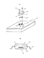
ICを測定・検査するのに、例えば、特許文献1に開示のようなIC評価治具を用いる方法が知られている。このIC評価治具は、図4(A)に概略を示すように、被側定IC1をアプリケーションボード2上に、ガイド枠6により所定の位置に固定部材4で固定する構成である。アプリケーションボード2には、被側定IC1のリード1aに対応付けられたパッド電極3が形成され、このパッド電極3上に導電性シート5が載置される。この導電性シート5は、絶縁性弾性部材の厚さ方向に金属繊維からなる多数の導電素子が貫通し、表面と裏面の対応部位が導電性で、面の広がり方向に絶縁性を示す異方性を有する導電性シートである。
In order to measure and inspect an IC, for example, a method using an IC evaluation jig as disclosed in Patent Document 1 is known. As schematically shown in FIG. 4A, this IC evaluation jig is configured to fix the fixed IC 1 on the
被側定IC1のリード1aは、固定部材4により押圧固定されたとき、導電性シート5を介してアプリケーションボード2の対応するパッド電極3に電気的に接続される。導電性シート5には弾力性があるため、リード1aの高さや厚さにバラツキがあっても良好な接触状態を保持し測定精度を高めることができるとされている。しかし、アプリケーションボード2上の導電パターンでインピーダンス整合が保たれていたとしても、導電性シート5を介しての厚さ方向の接続では整合がとり難く、インピーダンス不整合により信号波形に乱れが生じ、正確な評価ができなくなる恐れがある。
When the lead 1 a of the fixed IC 1 is pressed and fixed by the fixing member 4, the lead 1 a is electrically connected to the corresponding pad electrode 3 of the
また、特許文献2には、被側定ICのリードに接触子ピンを当てて評価・検査する方法が開示されている。この方法は、図4(B)に示すように、位置決め治具7上に被評価IC1を載置して位置決めし、上方から固定板8に取りつけられた接触子スタンド9bで押さえる。接触子スタンド9bには、接触子ピン9がバネ9aにより付勢されて挿着してあり、被側定IC1のリード1aに上方から接触され、また、接触子スタンド9bの中央部に配されたバネで被側定IC1の本体部を位置決め治具7上に押し付けて固定している。
この方法による被側定ICの評価・検査は、リード1aと接触子ピン9との間に異物や酸化膜等が介在して接触不良が生じやすい。このため、位置決め治具6を振動発生装置で接触面をこすり合わせて接触面を良好にする必要がある。また、このような接触子による接続構造では、高周波でのインピーダンス整合を満足させることは難しく、高周波用途のIC評価には不向きである。
In the evaluation / inspection of the fixed IC by this method, a contact failure is likely to occur due to the presence of foreign matter, an oxide film or the like between the lead 1a and the
したがって、数百MHz帯を越える帯域でのICの測定・検査では、低周波帯の測定で一般的なIC評価治具を用いると、ICのリードと配線パターンや接触子ピンとの接続でインピーダンス不整合が生じやすい。測定・検査治具の導電部をインピーダンス整合条件を満たすようにするには、通常の構造や大きさでは難しく、実現できたとしても特殊部品を使用したり、大型の装置となってしまう等の問題がある。
高周波用のICの測定・検査を行なう場合、被測定ICのリードとの接続部におけるインピーダンス整合を考慮しなければならない。これには、被測定ICのリードと電気測定端子との接続構造は、ICのリードを評価用の配線基板上に設けた配線パターンに直接接触させる構造を取らざるを得ない。しかしながら、一般のICは、そのリード形状がガルウィングタイプであるというものの同一の公差内で形成されているとは言い難く、ICのパッケージ外形もばらついている。また、増幅器用のICは発熱が大きく、このためIC底面にヒートスラグと呼ばれる放熱のための金属板を結合させ、パッケージ面の下面側に露出させた構造となっている。被測定ICの測定の際に、放熱が仕様通りになされないと、ICの温度上昇が大きくなりICの動作点がずれ、規定のAC特性が測定できなくなる。 When measuring and inspecting a high frequency IC, impedance matching at the connection portion with the lead of the IC to be measured must be considered. For this purpose, the connection structure between the lead of the IC to be measured and the electrical measurement terminal must be a structure in which the lead of the IC is directly brought into contact with the wiring pattern provided on the wiring board for evaluation. However, although a general IC has a gullwing type lead shape, it is difficult to say that the IC is formed within the same tolerance, and the package outline of the IC also varies. Further, the amplifier IC generates a large amount of heat. Therefore, a metal plate for heat dissipation called heat slag is coupled to the bottom surface of the IC and is exposed on the lower surface side of the package surface. When the measurement of the IC to be measured is not performed according to the specifications, the temperature rise of the IC increases, the IC operating point shifts, and the specified AC characteristics cannot be measured.
IC評価治具は、通常、配線基板側にICのリード幅やリード間隔に一致したパターンで配線用のパッド電極が形成され、また、ICのヒートスラグと接触して熱放散が行なえる放熱部が設けられている。被測定ICは、そのリードが配線基板上のパッド電極に一致するように載置した後、固定部材で押さえ付け、リードとパッド電極と確実に電気接触させ、且つヒートスラグを放熱部に密着させて放熱が良好になされるように構成されている。 IC evaluation jigs usually have a pad electrode for wiring formed in a pattern that matches the lead width and lead interval of the IC on the wiring board side, and a heat radiating part that can dissipate heat by contacting the heat slug of the IC Is provided. After the IC to be measured is placed so that the lead coincides with the pad electrode on the wiring board, it is pressed by a fixing member to ensure electrical contact between the lead and the pad electrode, and the heat slug is brought into close contact with the heat radiating part. In this way, the heat dissipation is good.
しかし、ICのリードの高さ位置やリード幅にバラツキがあったり、ICのパッケージ厚さが、規定値より薄かったり、反対に厚かったりすることがある。このような場合、例えば、ICのパッケージ厚さが規定値より薄い場合は、リードはパッド電極に電気接触させることはできるが、ヒートスラグは放熱部との密着不良乃至は浮いた状態となることがある。また、ICのパッケージ厚さが規定値より厚い場合は、ヒートスラグは放熱部に密着するも、リードが配線基板から浮き上がって、パッド電極との接続ができなくなることがある。 However, the IC lead height position and lead width may vary, and the IC package thickness may be thinner than a specified value or may be thicker. In such a case, for example, when the IC package thickness is thinner than a specified value, the lead can be brought into electrical contact with the pad electrode, but the heat slug is in poor contact with the heat radiating portion or is in a floating state. There is. In addition, when the IC package thickness is thicker than the specified value, the heat slug may be in close contact with the heat radiating portion, but the lead may be lifted from the wiring board and cannot be connected to the pad electrode.
本発明は、上述した実情に鑑みてなされたもので、被測定ICのリードの高さ位置にバラツキがあったり、ICのパッケージ厚さが、規定値より薄かったり厚かったりしても、リードを配線基板上のパッド電極に確実に接触させると共に、ヒートスラグを放熱部に密着させて所定の熱放散が行なわれるようにしたIC評価治具の提供を課題とする。 The present invention has been made in view of the above-described circumstances, and even if the lead height position of the IC to be measured varies, or even if the IC package thickness is thinner or thicker than the specified value, the lead is removed. It is an object of the present invention to provide an IC evaluation jig in which predetermined heat dissipation is performed by bringing a heat slag into close contact with a heat radiating portion while reliably contacting a pad electrode on a wiring board.
本発明によるIC評価治具は、リードピンを有する集積回路(IC)の高周波特性を試験するためのIC評価治具であって、収納部と押さえ部とを含む押さえ部材と、ICに高周波信号を供給若しくはICから高周波信号を送出するための配線パターンを有する配線基板とで構成され、ICを収納部に収納し、押さえ部によりICのリードピンを配線パターンに押さえつけることで、高周波試験を可能とするものである。押さえ部と収納部とは、同一の樹脂により一体成形で形成され、また、収納部は箱状の凹部を有し、押さえ部は凹部を構成する一対の側壁を含み、一対の側壁の端部に切り欠きが設けられ、側壁には厚さ方向に貫通する複数の孔が形成される。 An IC evaluation jig according to the present invention is an IC evaluation jig for testing high frequency characteristics of an integrated circuit (IC) having a lead pin, and includes a holding member including a storage portion and a holding portion, and a high frequency signal to the IC. It is composed of a wiring board having a wiring pattern for supplying or sending a high-frequency signal from the IC. The IC is housed in the housing portion, and the lead pin of the IC is pressed against the wiring pattern by the holding portion, thereby enabling a high-frequency test. Is. The presser part and the storage part are integrally formed of the same resin, and the storage part has a box-shaped recess, and the presser part includes a pair of side walls constituting the recess, and ends of the pair of side walls. A plurality of holes are formed through the side wall in the thickness direction.
本発明によれば、被測定ICの形状、寸法等に多少のバラツキがあっても、配線基板への電気的接続及び放熱のための物理的接触を確実に形成して、インピーダンス整合のとれた正確な高周波特性の測定・検査を行なうことができる。また、このための評価は、複雑なバネ機構を用いることなく簡単な構成で、安価に実施することができる。 According to the present invention, even if there is some variation in the shape, size, etc. of the IC to be measured, the electrical connection to the wiring board and the physical contact for heat dissipation are reliably formed, and impedance matching can be achieved. Accurate high-frequency characteristics can be measured and inspected. Moreover, the evaluation for this can be implemented inexpensively with a simple configuration without using a complicated spring mechanism.
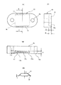
図により本発明の実施の形態を説明する。図1(A)は本発明の概略を説明する図、図1(B)は被測定ICの概略を説明する図である。図中、10は被測定IC、11は半導体チップ、12はリードピン、12aはボンディングワイヤ、13はヒートスラグ、14はパッケージ樹脂、15はIC押さえ部材、16は収納部、17は押さえ部、18は取付け孔、19は配線基板、20は配線パターン、21はパッド電極、22は放熱部、23は固定孔、24は固定部材を示す。 Embodiments of the present invention will be described with reference to the drawings. FIG. 1A is a diagram for explaining the outline of the present invention, and FIG. 1B is a diagram for explaining the outline of an IC to be measured. In the figure, 10 is an IC to be measured, 11 is a semiconductor chip, 12 is a lead pin, 12a is a bonding wire, 13 is a heat slug, 14 is a package resin, 15 is an IC pressing member, 16 is a storage portion, 17 is a pressing portion, 18 Is a mounting hole, 19 is a wiring board, 20 is a wiring pattern, 21 is a pad electrode, 22 is a heat radiating portion, 23 is a fixing hole, and 24 is a fixing member.
本発明によるIC評価治具は、図1(A)に示すように、被測定IC10をIC押さえ部材15内に収納して評価用の配線基板19上に載置固定する構成である。被測定IC10は、図1(B)に一例として示すような形状のもので、半導体基板上に各種トランジスタ等の能動素子や抵抗、容量等の受動素子が一体化したモノシリックマイクロ波集積回路等の半導体チップ11をパッケージ樹脂14で封止して構成される。半導体チップ11は、ボンディングワイヤ12aによりリードピン12に接続され、また、熱放散のためのヒートスラグ13と熱的に結合されている。
As shown in FIG. 1A, an IC evaluation jig according to the present invention has a configuration in which an
リードピン12は、通常、パッケージ樹脂14の両側部から突き出るガルウィングタイプのものが多く使用されているが、本発明で対象とする被測定IC10も、このタイプのリードピンで形成されているものとする。また、ヒートスラグ13は、Cu等の熱伝導性のよい金属板からなり、ICのパッケージ樹脂14の下面側に露出された状態で形成されていることが好ましい。露出されたヒートスラグ13は、搭載基板等に設けられた放熱部に直接接合されて効率よく熱放散が行なわれ、チップ内の動作素子が適正に動作するようにされているのが望ましい。
The
上述のような被測定IC10は、測定・検査のために合成樹脂で一体成形されたIC押さえ部材15内に収納される。IC押さえ部材15は、被測定IC10を収納する収納部16とリードピン12を押さえる押さえ部17を有している。また、被測定IC10を収納保持して、評価用の配線基板19上に固定するための取付け孔18を有し、この取付け孔18にねじ等の固定部材24を挿入して、被測定IC10を所定の位置に固定する。
The
配線基板19は、例えば、アルミ等の金属基板上に絶縁基板を設けて形成され、その表面には、ICに高周波信号を供給若しくはICから高周波信号を送出するための配線パターン20、パッド電極21、放熱部22等が形成されている。また、固定部材24を受ける固定孔23等も形成されている。パッド電極21は被測定IC10のリードピン12の配列、寸法等に対応するパターンで形成され配線パターン20に電気的に接続されている。放熱部22は、被測定ICのヒートスラグ13と密接に接触して、被測定ICで発生される熱を金属基板を介して放散するように形成されている。
For example, the
上述の如く構成されたIC評価治具は、IC押さえ部材15の収納部16内に被測定IC10を収納し、被測定IC10のリードピン12が配線基板19のそれぞれにパッド電極21に対応するように載置する。次いで、固定部材24を締付けることにより、IC押さえ部材15の押さえ部17が弾性的に撓んでリードピン12をパッド電極21に押しつけ、電気的接続を形成する。また、IC押さえ部材15の収納部16の基壁で被側定IC10のパッケージ上面を押圧し、下面側のヒートスラグ13を放熱部22の表面に密接させる。
The IC evaluation jig configured as described above accommodates the IC to be measured 10 in the
しかしながら、リードピン12の高さ位置やICのパッケージ厚さには、多少のバラツキがある。このため、IC押さえ部材15の押さえ部17の弾性が適正でない(硬すぎ或いは軟らかすぎ)場合、リードピン12とパッド電極21との電気的接続が不十分となったり、ヒートスラグ13が放熱部22に密接しなかったりする。この結果、ICの動作状態が変動し、正しい評価ができなくなる。
However, there is some variation in the height of the lead pins 12 and the IC package thickness. For this reason, when the elasticity of the
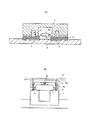
本発明においては、このようなことを回避するために、IC押さえ部材15の押さえ部17で適度の弾性変形が得られるようにしている。図2は、そのための一例を示す図で、図2(A)は平面図、図2(B)は端面図、図2(C)は側面図、図2(D)は被側定ICを示す図である。図中、15aはIC押さえ部材の下端、16aは収納部の基壁、17aは切り欠き、17bは押さえ部下端、17cは貫通孔を示す。その他の符号は図1の説明で用いたのと同じ符号を用いることにより説明を省略する。
In the present invention, in order to avoid such a situation, an appropriate elastic deformation is obtained by the
IC押さえ部材15は、図1で概略を説明したように、被測定IC10を収納する収納部16とリードピン12を押さえる押さえ部17を有している。収納部16は、被測定IC10がすっぽり入る広さの箱状の凹部を有し、IC押さえ部材の下端15aからの深さ寸法Hは、被測定IC10のパッケージ厚さDより僅かに小さく設定される。これにより、被測定IC10をIC押さえ部材15で押さえたとき、収納部の基壁16aは被測定IC10の上面に当たって、被測定IC10の下面を配線基板上に密着させることができる。
The
収納部16の凹部の一対の側壁は、弾性変形が可能な押さえ部17とされ、被測定IC10の両側から突き出る複数のリードピン12を上方から押さえ、配線基板上のパッド電極に押圧接触させる。押さえ部17は、IC押さえ部材15の本体部とは別の弾性変形が可能な材料で形成することもできるが、IC押さえ部材15の本体部と同一の樹脂材で一体成形で形成するのが簡単であり好ましい。これにより、別の材料で形成したときの構造上の複雑さや結合強度不足を回避でき、コスト的にも安価なものとすることができる。
The pair of side walls of the concave portion of the
また、押さえ部17となる側壁の端部に切り欠き17aを設け、本体部分とは独立して弾性変形が可能とする構成が好ましい。これにより、その押さえ部下端17bは、被測定IC10の両側から突き出る複数のリードピン12を均一に押圧し、部分的な接触不良が生じないようにすることができる。なお、押さえ部下端17bは、予めリードピン12の厚さdに相当する分だけ、IC押さえ部材の下端15aより減じた寸法hとして、過度の弾性変形が生じないようにしておくのが望ましい。
Moreover, the structure which provides the
押さえ部17を弾性変形が可能とするのに、成形材料自体に弾性材を用いたり、厚さを薄くするなどの方法もある。しかし、IC押さえ部材15と一体成形するような場合、成形材料に弾性材を用いるとIC押さえ部材15の本体部も変形してしまい、被測定IC10を固定するのに好ましくない場合がある。また、押さえ部17を薄く形成すると、機械的に弱くなり破断が生じたり、側方によれたりして押圧力が不足する場合がある。
In order to allow the
そこで、押さえ部17となる側壁には厚さ方向に貫通する貫通孔17cを多数設け、多孔形状にして弾性変形が可能なようにすることができる。この形状は、押さえ部17が側方によれずにリードピンの厚さ方向に圧縮されるように弾性変形するので、公差を効果的に吸収して押圧力を高めることができる。また、リードピンの厚さ方向に貫通孔17cの孔の大きさや形成密度を変えることで、押さえ部17の弾性を調整することができる。なお、貫通孔の孔形状は特に限定されないが、形成の容易性から円形孔で形成するのが好ましい。
Therefore, a large number of through-
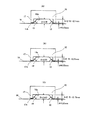
図3は、以上のように形成したIC押さえ部材15を用いて、被測定IC10を配線基板19上に載置固定する使用形態を説明する図で、図2のA−A’方向から見るときの断面で示してある。ここで、図2で示した被測定IC10のパッケージ厚さDを2.35mm±0.05mm、リードピン12の厚さdを0.25mmとする。そして、IC押さえ部材15の下端15aからの深さ寸法Hは、パッケージ厚さDの下限値となる2.3mmとし、押さえ部17側の寸法hは、2.15mmとしたものとする。
FIG. 3 is a diagram for explaining a usage mode in which the
図3(A)は、被測定IC10のパッケージ厚さDが、規定値の2.35mmで形成されている場合である。収納部の深さ寸法H=2.3mmであるので、IC押さえ部材15の下端15aと配線基板19との間は0.05mmの間隙が残っていて、被測定IC10の下面は、配線基板19の放熱部に密着する状態で固定される。押さえ部17側のh=2.15mmは2.10mmに弾性変形し、リードピン12を配線基板19上のパッド電極に押圧して良好な電気接続が得られる。
FIG. 3A shows a case where the package thickness D of the IC to be measured 10 is formed with a specified value of 2.35 mm. Since the depth H of the housing portion is 2.3 mm, a gap of 0.05 mm remains between the
図3(B)は、被測定IC10のパッケージ厚さDが、規定の下限値である2.30mmで形成されている場合である。収納部の深さ寸法H=2.3mmであるので、IC押さえ部材15の下端15aと配線基板19との間隙はゼロとなるが、被測定IC10の下面は、配線基板19上の放熱部にほぼ密着する状態で固定される。押さえ部17側のh=2.15mmは2.05mmに弾性変形し、リードピン12を配線基板19上のパッド電極に押圧して良好な電気接続が得られる。
FIG. 3B shows a case where the package thickness D of the IC to be measured 10 is formed with a prescribed lower limit of 2.30 mm. Since the depth dimension H of the housing portion is 2.3 mm, the gap between the
図3(C)は、被測定IC10のパッケージ厚さDが、規定の上限値である2.40mmで形成されている場合である。収納部の深さ寸法H=2.3mmであるので、IC押さえ部材15の下端15aと配線基板19との間は0.1mmの間隙が残っていて、被測定IC10の下面は、配線基板19の放熱部に密着する状態で固定される。押さえ部17側のh=2.15mmは弾性変形がなく2.15mmのままであるが、リードピン12と配線基板19上のパッド電極との間の隙間はゼロであるので、電気接続は問題なく得ることができる。
FIG. 3C shows a case where the package thickness D of the
10…被測定IC、11…半導体チップ、12…リードピン、12a…ボンディングワイヤ、13…ヒートスラグ、14…パッケージ樹脂、15…IC押さえ部材、15a…IC押さえ部材の下端、16…収納部、16a…収納部の基壁、17…押さえ部、17a…切り欠き、17b…押さえ部下端、17c…貫通孔、18…取付け孔、19…配線基板、20…配線パターン、21…パッド電極、22…放熱部、23…固定孔、24…固定部材。
DESCRIPTION OF
Claims (4)
収納部と押さえ部とを含む押さえ部材と、前記ICに高周波信号を供給若しくは前記ICから高周波信号を送出するための配線パターンを有する配線基板とで構成され、前記ICを前記収納部に収納し、前記押さえ部により前記ICのリードピンを前記配線パターンに押さえつけることを特徴とするIC評価治具。 An IC evaluation jig for testing high frequency characteristics of an integrated circuit (IC) having lead pins,
The holding member includes a holding part and a holding part, and a wiring board having a wiring pattern for supplying a high frequency signal to the IC or sending a high frequency signal from the IC. The IC is stored in the receiving part. An IC evaluation jig, wherein the lead pin of the IC is pressed against the wiring pattern by the pressing portion.
Priority Applications (1)
| Application Number | Priority Date | Filing Date | Title |
|---|---|---|---|
| JP2004105543A JP2005291847A (en) | 2004-03-31 | 2004-03-31 | IC evaluation jig |
Applications Claiming Priority (1)
| Application Number | Priority Date | Filing Date | Title |
|---|---|---|---|
| JP2004105543A JP2005291847A (en) | 2004-03-31 | 2004-03-31 | IC evaluation jig |
Publications (1)
| Publication Number | Publication Date |
|---|---|
| JP2005291847A true JP2005291847A (en) | 2005-10-20 |
Family
ID=35324946
Family Applications (1)
| Application Number | Title | Priority Date | Filing Date |
|---|---|---|---|
| JP2004105543A Pending JP2005291847A (en) | 2004-03-31 | 2004-03-31 | IC evaluation jig |
Country Status (1)
| Country | Link |
|---|---|
| JP (1) | JP2005291847A (en) |
Cited By (3)
| Publication number | Priority date | Publication date | Assignee | Title |
|---|---|---|---|---|
| KR101096776B1 (en) * | 2009-11-19 | 2011-12-21 | 주식회사 피플웍스 | Transistor fixing plate |
| CN103713256A (en) * | 2013-12-25 | 2014-04-09 | 中山市拓电电子科技有限公司 | Dual compression method used for cpu automatic pick-and-place machine |
| CN115236578A (en) * | 2022-08-15 | 2022-10-25 | 深圳振华富电子有限公司 | Sensor electrical property test fixture |
-
2004
- 2004-03-31 JP JP2004105543A patent/JP2005291847A/en active Pending
Cited By (3)
| Publication number | Priority date | Publication date | Assignee | Title |
|---|---|---|---|---|
| KR101096776B1 (en) * | 2009-11-19 | 2011-12-21 | 주식회사 피플웍스 | Transistor fixing plate |
| CN103713256A (en) * | 2013-12-25 | 2014-04-09 | 中山市拓电电子科技有限公司 | Dual compression method used for cpu automatic pick-and-place machine |
| CN115236578A (en) * | 2022-08-15 | 2022-10-25 | 深圳振华富电子有限公司 | Sensor electrical property test fixture |
Similar Documents
| Publication | Publication Date | Title |
|---|---|---|
| JP7336176B2 (en) | Inspection jig | |
| JP5225257B2 (en) | Socket for semiconductor chip inspection | |
| KR101073400B1 (en) | Test probe | |
| JP2005291847A (en) | IC evaluation jig | |
| JP4213455B2 (en) | Socket for electrical parts | |
| JP2004340867A (en) | Spring probe and ic socket | |
| KR20110087539A (en) | Probe card and its manufacturing method | |
| TWI635281B (en) | Contact unit and inspection fixture | |
| JPH0566243A (en) | Jig for lsi evaluation | |
| JP2011180019A (en) | Apparatus for measuring semiconductor, and pitch conversion tool for the same | |
| KR100714569B1 (en) | Semiconductor Integrated Circuit Tester | |
| JP3390572B2 (en) | Transport contact structure for electronic devices | |
| JP2000304769A (en) | probe | |
| JP4765508B2 (en) | Measuring jig for high frequency devices | |
| JP3815165B2 (en) | Electronic component measuring device | |
| JP5126009B2 (en) | Test method, test apparatus and semiconductor device manufacturing method | |
| WO2007026563A1 (en) | Calibration board for electronic component testing apparatus | |
| JP2001217280A (en) | Semiconductor mounting structure | |
| JP3172305B2 (en) | Method for manufacturing semiconductor device | |
| JPH0735771A (en) | Jig for testing electrical characteristics of semiconductor devices | |
| JP2000133398A (en) | socket | |
| WO2000014833A1 (en) | Socket for handler | |
| JP2000082553A (en) | Socket for IC | |
| JPH09329646A (en) | Semiconductor device testing equipment | |
| JP2007141611A (en) | Socket for measurement and manufacturing method of semiconductor device |