JP2005291845A - Surface flaw inspection device - Google Patents
Surface flaw inspection device Download PDFInfo
- Publication number
- JP2005291845A JP2005291845A JP2004105463A JP2004105463A JP2005291845A JP 2005291845 A JP2005291845 A JP 2005291845A JP 2004105463 A JP2004105463 A JP 2004105463A JP 2004105463 A JP2004105463 A JP 2004105463A JP 2005291845 A JP2005291845 A JP 2005291845A
- Authority
- JP
- Japan
- Prior art keywords
- defect
- inspected
- light emitting
- imaging
- unit
- Prior art date
- Legal status (The legal status is an assumption and is not a legal conclusion. Google has not performed a legal analysis and makes no representation as to the accuracy of the status listed.)
- Granted
Links
Images


Classifications
-
- G—PHYSICS
- G01—MEASURING; TESTING
- G01N—INVESTIGATING OR ANALYSING MATERIALS BY DETERMINING THEIR CHEMICAL OR PHYSICAL PROPERTIES
- G01N21/00—Investigating or analysing materials by the use of optical means, i.e. using sub-millimetre waves, infrared, visible or ultraviolet light
- G01N21/84—Systems specially adapted for particular applications
- G01N21/88—Investigating the presence of flaws or contamination
- G01N21/95—Investigating the presence of flaws or contamination characterised by the material or shape of the object to be examined
- G01N21/9515—Objects of complex shape, e.g. examined with use of a surface follower device
-
- G—PHYSICS
- G01—MEASURING; TESTING
- G01N—INVESTIGATING OR ANALYSING MATERIALS BY DETERMINING THEIR CHEMICAL OR PHYSICAL PROPERTIES
- G01N21/00—Investigating or analysing materials by the use of optical means, i.e. using sub-millimetre waves, infrared, visible or ultraviolet light
- G01N21/84—Systems specially adapted for particular applications
- G01N21/88—Investigating the presence of flaws or contamination
- G01N21/8806—Specially adapted optical and illumination features
- G01N2021/8829—Shadow projection or structured background, e.g. for deflectometry
-
- G—PHYSICS
- G01—MEASURING; TESTING
- G01N—INVESTIGATING OR ANALYSING MATERIALS BY DETERMINING THEIR CHEMICAL OR PHYSICAL PROPERTIES
- G01N2201/00—Features of devices classified in G01N21/00
- G01N2201/06—Illumination; Optics
- G01N2201/062—LED's
- G01N2201/0626—Use of several LED's for spatial resolution
Landscapes
- Physics & Mathematics (AREA)
- Health & Medical Sciences (AREA)
- Life Sciences & Earth Sciences (AREA)
- Chemical & Material Sciences (AREA)
- Analytical Chemistry (AREA)
- Biochemistry (AREA)
- General Health & Medical Sciences (AREA)
- General Physics & Mathematics (AREA)
- Immunology (AREA)
- Pathology (AREA)
- Investigating Materials By The Use Of Optical Means Adapted For Particular Applications (AREA)
Abstract
Description
本発明は、所定のレイアウトパターンで配置された複数の発光素子と、前記発光素子の照射光によって照明された被検査面を撮像する撮像カメラと、前記撮像カメラの撮像情報を出力する出力部とを備え、前記出力部からの出力信号を評価して前記被検査面における欠陥を検知する欠陥評価部を備えた表面欠陥検査装置に関する。 The present invention includes a plurality of light emitting elements arranged in a predetermined layout pattern, an imaging camera that images a surface to be inspected illuminated by light emitted from the light emitting elements, and an output unit that outputs imaging information of the imaging camera. And a surface defect inspection apparatus including a defect evaluation unit that evaluates an output signal from the output unit and detects a defect on the surface to be inspected.
この種の表面欠陥検査装置の代表例として、自動車ボディ(具体的にはバンパー)の塗装面の検査に使用される技術を挙げることができる。このような表面欠陥検査では、被検査面としての塗装面上に存する凹凸や傷等が、その検査対象となる。
発光面でパターンを成す検査光を使用する検査技術として、所謂、ストライプ状、即ち、横縞模様の明暗を作り出している照射光を塗装面に照明して、照明状態にある塗装面を撮像カメラにより撮像し、得られる撮像画像を用いて表面検査を行う技術がある。
A typical example of this type of surface defect inspection apparatus is a technique used for inspecting the painted surface of an automobile body (specifically, a bumper). In such a surface defect inspection, irregularities, scratches, etc. existing on the painted surface as the surface to be inspected are the inspection objects.
As an inspection technique that uses inspection light that forms a pattern on the light-emitting surface, the painted surface is illuminated with so-called stripes, that is, horizontal stripes of light and darkness. There is a technique for imaging and performing surface inspection using the obtained captured image.
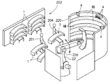
この種の検査システムの具体的構成を図10に示した。
図10に示す欠陥検査システムにあっては、検査対象となる複数のバンパーがストックされたストックステーション202から、投入員204が随時、バンパー1を取り出し、バンパー1を保持して姿勢変更するロボット22に取り付ける。
A specific configuration of this type of inspection system is shown in FIG.
In the defect inspection system shown in FIG. 10, the robot 22 changes the posture by holding the
ロボット22はバンパー1を保持したまま、図10に示す回転軸22d周りに回転させ、バンパー1を姿勢変更する。この姿勢変更に対応して、システムには所定の横縞パターンで光を照明する照明装置220が備えられている。図示する例にあっては、バンパー1が姿勢変更を行う移動空間を囲むように、この装置220が設けられている。照射光の照明パターンは、バンパー1の回転軸22dに平行なストライプ状の明暗パターンである。
The robot 22 rotates around the
照明装置220の所定箇所には、複数の撮像カメラ4が設けられており、これらカメラ4によりバンパー1に写り込んだ照射光の明暗パターンが撮像される。撮像結果は、解析側へ送られ、欠陥の有無等の評価が行われる。
A plurality of
ロボット22より下手側に位置する検査員201は、ロボット22による保持・姿勢変更を終了した後、バンパー1を取り外し、目視検査等の後工程におくる。
The
この時、検査員201は欠陥評価手段からの評価情報を得ており、検査において注目すべき箇所の情報をえており、迅速確実に作業を進める。
At this time, the
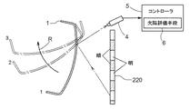
この構成の表面欠陥検査の基本原理を示したのが、図11である。
同図に示すように、塗装面を所定方向(例えばR方向)に移動させていった場合に、塗装面上にある凹凸面といった欠陥の画像部分が、前記移動方向Rに直交する方向(例えば図11における紙面表裏方向)の座標を変えることなく、その方向座標(R座標)を変えながら撮像されることを利用して、欠陥の検出を行うことができる。即ち、欠陥領域は撮像画像において、明のストライプ部位では暗く、暗のストライプ部位では明るく撮像されことを利用して欠陥を識別することから、欠陥は、ストライプの明部分及び暗部分の中間階調画像として捕らえることができる。同様の検査原理を使用する技術が、特許文献1に示されている。
FIG. 11 shows the basic principle of the surface defect inspection with this configuration.
As shown in the figure, when the painted surface is moved in a predetermined direction (for example, R direction), a defective image portion such as an uneven surface on the painted surface is perpendicular to the moving direction R (for example, It is possible to detect a defect by changing the direction coordinates (R coordinates) without changing the coordinates of the paper front and back directions in FIG. In other words, in the captured image, the defect is identified by utilizing the fact that the image is dark in the bright stripe part and bright in the dark stripe part. It can be captured as an image. A technique that uses a similar inspection principle is disclosed in Japanese Patent Application Laid-Open No. H10-228707.
さらに、表面の周期的な凹凸である「ゆず肌」と呼ばれる欠陥を検出しようとするために、照射光である明暗ストライプの境界線の撮像画像上でのゆらぎにより塗装厚みの班を見出そうとするものがある(特許文献2参照)。 Furthermore, in order to detect a defect called “Yuzu skin”, which is a periodic unevenness on the surface, let's find a group of paint thickness by fluctuation on the captured image of the boundary line of light and dark stripes that are irradiation light (See Patent Document 2).
この検査手法では、被検査面を移動させる必要はないが、概して、塗装面の比較的広い範囲に渡ってストライプの境界線画像に位置ずれを起こさせるような乱れが発生している塗装面が検出対象となる。 In this inspection method, it is not necessary to move the surface to be inspected, but in general, there is a paint surface on which a disturbance that causes displacement in the boundary image of the stripe occurs over a relatively wide range of the paint surface. It becomes a detection target.
特許文献1及び2のような従来の表面欠陥検査手法では、被検査面を照明する照明部がストライプ状の明暗パターンを塗装面に照明するので、表面検査に用いる照射光の回り込みは、ストライプ状の明暗パターンと直交(横断)する方向でしか発生しない。結果、被検査面に、このストライプパターンのストライプ方向(ストライプの延長方向と同方向)に欠陥が存在した場合において、この種の欠陥が捕らえにくい。
In the conventional surface defect inspection methods such as
さらにこの技術では、実質上、凸状欠陥しか抽出できず、写り込み箇所について明暗差を得難く二値価処理で誤検出が出やすい。また、意匠ライン及びその近傍の欠陥が捉えにくい。 Furthermore, with this technique, only convex defects can be substantially extracted, and it is difficult to obtain a light / dark difference at a reflected portion, and erroneous detection is likely to occur in binary value processing. In addition, it is difficult to catch design lines and defects in the vicinity thereof.
さらに、図10,11に示すように、検査に使用する照射光の照明光軸と、撮像カメラの撮像光軸との方向が交差するために、撮像カメラに取り込める光量の点で充分でなく改善の余地がある。また、このような検査系においては光学的な複雑さから、欠陥評価側の処理も複雑にならざるを得ない。同時に、照射系、撮像系の位置関係を厳密なものとする必要が生じる。 Furthermore, as shown in FIGS. 10 and 11, since the direction of the illumination optical axis of the irradiation light used for the inspection and the imaging optical axis of the imaging camera intersect, it is not sufficient in terms of the amount of light that can be captured by the imaging camera. There is room for. Further, in such an inspection system, the processing on the defect evaluation side must be complicated due to optical complexity. At the same time, the positional relationship between the irradiation system and the imaging system needs to be strict.
本発明の目的は、所定のレイアウトパターンで配置された複数の発光素子からなる照射系と、その照射系から照明される照射光を受けた被検査面を撮像する撮像カメラとを備える表面欠陥検査装置において、照射系と撮像系との構成が最も合理的かつシンプルであり、信頼性の高い検査を行うことが可能な表面欠陥検査装置を得ることにある。 SUMMARY OF THE INVENTION An object of the present invention is to provide a surface defect inspection comprising an irradiation system composed of a plurality of light emitting elements arranged in a predetermined layout pattern, and an imaging camera for imaging a surface to be inspected that has received irradiation light illuminated from the irradiation system. An object of the present invention is to obtain a surface defect inspection apparatus in which the configuration of the irradiation system and the imaging system is the most rational and simple and capable of performing highly reliable inspection.
上記目的を達成するための課題を解決するための、所定のレイアウトパターンで配置された複数の発光素子と、前記発光素子の照射光によって照明された被検査面を撮像する撮像カメラと、前記撮像カメラの撮像情報を出力する出力部とを備え、前記出力部からの出力信号を評価して前記被検査面における欠陥を検知する欠陥評価部を備えた表面欠陥検査装置の特徴構成は、
前記レイアウトパターンが前記発光素子を内側に所定形状の暗面を残すように連続的に配置させたものであり、少なくとも一つの前記暗面に前記撮像カメラが前記被検査面から反射される前記各発光素子の照射光を受光するように配置されるとともに、
前記複数の発光素子と前記少なくとも一つの撮像カメラとを一体として前記被検査面に沿って移動させる倣い装置を備えたことにある。
A plurality of light-emitting elements arranged in a predetermined layout pattern, an imaging camera that images a surface to be inspected illuminated by light emitted from the light-emitting elements, and the imaging An output unit that outputs imaging information of the camera, and a characteristic configuration of a surface defect inspection apparatus including a defect evaluation unit that detects a defect in the inspection target surface by evaluating an output signal from the output unit,
The layout pattern is a continuous arrangement of the light emitting elements so as to leave a dark surface of a predetermined shape on the inside, and the imaging camera is reflected from the surface to be inspected on at least one of the dark surfaces. It is arranged to receive the irradiation light of the light emitting element,
A copying apparatus is provided that moves the plurality of light emitting elements and the at least one imaging camera integrally along the surface to be inspected.
この欠陥検査装置においても、その検査原理として、照射光の回り込みを利用するが、この検査原理を利用する場合、照明部を、内側に所定形状の暗面を残すように配置された発光素子を連続的に配置したレイアウトパターンを使用する。 Even in this defect inspection apparatus, the wrapping of irradiation light is used as the inspection principle. When this inspection principle is used, the illumination unit is provided with a light emitting element arranged so as to leave a dark surface of a predetermined shape inside. Use continuously arranged layout patterns.
このようにすると、例えば、塗装面が平面で、照明部における発光素子のレイアウトパターンが六角形で、塗装面の法線方向に照射光の光軸および撮像カメラの光軸が向けられている場合、塗装面に欠陥がなければ撮像は六角形の明暗パターンとなる。しかしながら、欠陥がある場合、この欠陥により六角の内部に形成された暗面に中間輝度領域が、図7に示すような孤立点として形成される。
従って、この欠陥起因の像を撮像カメラで確実に撮像することができる。
In this case, for example, when the painted surface is flat, the layout pattern of the light emitting elements in the illumination unit is hexagonal, and the optical axis of the irradiation light and the optical axis of the imaging camera are directed in the normal direction of the painted surface If there is no defect on the painted surface, the imaging is a hexagonal light-dark pattern. However, if there is a defect, an intermediate luminance region is formed as an isolated point as shown in FIG. 7 on the dark surface formed inside the hexagon due to this defect.
Therefore, the image resulting from this defect can be reliably captured by the imaging camera.
しかも、暗面に撮像カメラを配置することで、照射光の光軸方向と撮像側の光軸方向を一致させることが可能となり、所謂、落射状態での撮像検査が可能となる。 In addition, by arranging the imaging camera on the dark surface, it is possible to match the optical axis direction of the irradiation light with the optical axis direction on the imaging side, so that an imaging inspection in a so-called epi-illumination state is possible.
そして、前記出力部からの出力信号を評価して前記被検査面における欠陥を検知する欠陥評価部を備える構成としておくと、画像処理技術として確立された技術を利用して、自動的に欠陥箇所を評価、割り出しできる。 And if it is set as the structure provided with the defect evaluation part which evaluates the output signal from the said output part and detects the defect in the said to-be-inspected surface, a defect location will be automatically utilized using the technique established as an image processing technique. Can be evaluated and determined.
また、複数の発光素子と少なくとも一つの撮像カメラとを一体として被検査面に沿って移動させる倣い装置を備えることで、これら光学機器を備えて構成される撮像ユニットを被検査面に対する位置関係(発光素子及び撮像カメラの光軸、さらに、照射面、撮像面と被検査面との距離等)を一定の状態として倣わせて、自動で信頼性の高い欠陥検査を実行できる。 In addition, by providing a copying apparatus that moves a plurality of light emitting elements and at least one imaging camera as a unit along the surface to be inspected, the positional relationship between the imaging unit including these optical devices and the surface to be inspected ( The optical axis of the light emitting element and the imaging camera, the irradiation surface, the distance between the imaging surface and the surface to be inspected, and the like can be traced as a constant state, and the defect inspection can be automatically performed with high reliability.
さらに、前記複数の発光素子の発光面と、前記撮像カメラの撮像面が同一平面内にあるものとし、前記倣い装置により、その同一平面を被検査面に対して平行に維持することが好ましい。
この種の検査にあっては、撮像画像における画像の明るさ、さらには、その画像部位の位置等は、発光面と撮像面とに対する被検査面の位置関係に大きく影響される。その点、発光面と撮像面とを同一平面上に位置させることで、これらが一体化した撮像ユニットを容易に構築でき、この同一平面から被検査面までの距離の調節だけで、検査における光学構成を実質上特定することが可能となり、検査の信頼性をこの点からも確立できる。
Furthermore, it is preferable that the light emitting surfaces of the plurality of light emitting elements and the imaging surface of the imaging camera are in the same plane, and the same plane is maintained parallel to the surface to be inspected by the copying apparatus.
In this type of inspection, the brightness of the image in the captured image, and further the position of the image part, etc. are greatly affected by the positional relationship of the surface to be inspected with respect to the light emitting surface and the imaging surface. In that respect, by positioning the light emitting surface and the imaging surface on the same plane, it is possible to easily construct an imaging unit that integrates them, and only by adjusting the distance from the same plane to the surface to be inspected, the optical unit for inspection The configuration can be substantially specified, and the reliability of the inspection can be established from this point.
さて、前記レイアウトパターンが、所定方向において繰り返される繰り返しレイアウトパターンであることが好ましい。 The layout pattern is preferably a repeated layout pattern that is repeated in a predetermined direction.
このような繰り返しパターンとすることで、例えば、発光素子のレイアウトパターン部位とその内部に設けられる暗面とを単位として、撮像に対する画像処理を、同一の基準で繰り返し行うことができる。また、被検査面が移動している場合、同一の被検査面部位を繰り返し検査でき、当該被検査面部位について複数の撮像情報を得て、信頼性の高い検査を行うことができる。 By setting it as such a repeating pattern, the image processing with respect to imaging can be repeatedly performed on the same reference | standard, for example for the layout pattern site | part of a light emitting element, and the dark surface provided in the inside. Further, when the surface to be inspected is moving, it is possible to repeatedly inspect the same surface area to be inspected, and obtain a plurality of pieces of imaging information for the surface area to be inspected, thereby performing a highly reliable inspection.
さらに、前記被検査面を前記複数の発光素子及び前記撮像カメラに対して相対搬送移動する搬送機構を備え、
前記レイアウトパターンの繰り返し方向が前記相対搬送方向であることが好ましい。
この種の表面欠陥検査にあっては、被検査面が自動的に移動する状態で検査される場合もあり、所定のレイアウトパターンの繰り返しで、順次、特定の被検査面を繰り返して撮像し、撮像情報を得ることで、信頼性の高い検査を行える。
And a transport mechanism for transporting the surface to be inspected relative to the plurality of light emitting elements and the imaging camera.
It is preferable that a repeating direction of the layout pattern is the relative transport direction.
In this type of surface defect inspection, the surface to be inspected may be inspected in a state where it automatically moves, and by repeating a predetermined layout pattern, a specific surface to be inspected is repeatedly imaged sequentially, By obtaining imaging information, highly reliable inspection can be performed.
本発明によるその他の特徴及び利点は、以下図面を用いた実施形態の説明により明らかになるだろう。 Other features and advantages of the present invention will become apparent from the following description of embodiments using the drawings.
以下、本願の表面欠陥検査装置100に関して説明する。
本願の表面欠陥検査装置100は、図10に対応した図1に示す検査システム200に採用されるものであり、図1は、検査システム200の全体構成を、図2、3は表面欠陥検査装置100の全体構成を、図4は表面欠陥検査装置100の撮像ユニット300の構成を、図5は撮像情報の評価系の構成を示したものである。
Hereinafter, the surface
The surface
この検査システム200もまた、先に従来技術の項で説明したように、例えば、バンパー1の表面欠陥検査を目的とするものである。表面欠陥検査装置100は、このシステム200において、ストックステーション202の下手側、目視検査ステーション203の上手側に配設されており、この表面欠陥検査装置100には、本願独特の構成を有する撮像ユニット300が備えられている。
The
この撮像ユニット300はバンパー1の外形形状に倣って倣い動作することで、検査を従来より格段に高い精度かつ信頼性で行うことを可能としている。
以下、検査システム200の構成、表面欠陥検査装置100における撮像ユニット300の倣い構成、撮像画像の処理の順に詳細に説明する。
The
Hereinafter, the configuration of the
〔検査システム〕
図1に示すように、本願に係る検査システム200では、検査対象であるバンパー1の搬送ロボット2による移動経路が直線移動経路とされている。
図1において、検査対象のバンパー1は、図上、右上側から左下側へ搬送される。図示するように、検査は一対のバンパー1を一単位として行われる。従って、この搬送方向に沿って、ストックステーション202、表面欠陥検査装置100、目視検査ステーション203が設けられている。
ストックステーション202から搬送ロボット2へのバンパー1の移動が投入員204により行われ、検査員201によって目視検査が行われる点に関しては、従来通りである。
[Inspection system]
As shown in FIG. 1, in the
In FIG. 1, the
The
作業の流れに沿って説明すると、ストックステーション202から投入員204が随時一対のバンパー1を取り出し、搬送ロボット2のバンパー支持部2aに取り付ける。
If it demonstrates along a flow of work, the
搬送ロボット2は、バンパー1を保持したまま、搬送経路を下手側に移動する。このときバンパー1の姿勢変更は起こらず、搬送経路に沿って並進移動するのみである。バンパー1が表面欠陥検査装置100内に入ると、バンパー1の表面形状に倣うように、前述の撮像ユニット300が姿勢変更を伴って移動する。その移動形態は後述するように、撮像ユニット300の照明部3を検査面に平行に、且つ撮像カメラ4の光軸を検査面の法線方向に維持するもので、被検査面と撮像ユニット300との間の距離を一定とするものある。
The
そして、撮像ユニット300に備えられる複数の撮像カメラ4によりバンパー1に写り込んだ照射光の明暗パターンが撮像される。撮像結果は、解析側である欠陥評価手段6へ送られ、欠陥の有無等の評価が行われる。
Then, the light / dark pattern of the irradiation light reflected on the
搬送下手側に位置する検査員201は、送られてくるバンパー1を目視検査するのであるが、図1に示されるように、この時、検査員201は欠陥評価手段6からの評価情報を検査結果プロジェクタ15より、検査において注目すべき箇所情報としており、特にその箇所等を中心に目視検査を進めることができる。
The
〔表面欠陥検査装置における撮像ユニットの倣い構成〕
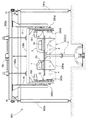
a 撮像ユニット300
図4に、撮像ユニット300の平面図(イ)、正面図(ロ)、平面視の詳細を(ハ)に示した。同図に示すように、撮像ユニット300は基本的には概略直方体形状を有したユニットフレーム300aと、このユニットフレーム300aの長手方向(図4(イ)におけるL1方向)の両端にユニットフレーム300aから上下方向に延びる揺動支持フレーム部300bを備えて構成されている。
[Following configuration of the imaging unit in the surface defect inspection apparatus]
a
FIG. 4 shows a plan view (A), a front view (B), and details of a plan view of the
同図にも示されるように、前記ユニットフレーム300aの上側端面は、本願にいう照明部3として構成されており、この照明部3には多数の発光素子30が六角形状を単位として繰り返しレイアウトで配設されている。
As shown in the figure, the upper end surface of the
さらに、この照明部3の幅方向中央には、所定均等間隔で撮像カメラ4のレンズ面4a(即ち撮像部)が備えられている。図示する例にはあっては、10個の撮像カメラ4を備えた例を示している。図4(ロ)に示すように、ユニットフレーム300aの内部には、撮像カメラ4および発行素子30用のDC電源300cが設けられている。
Furthermore, the
b 倣い装置による倣い構造
上述の撮像ユニット300は、前記揺動支持フレーム部300bの先端に設けられている左右一対の支持軸300dでユニット300が支持されるように構成されている。この支持軸300dは、その軸心周りの回転が可能とされるとともに、表面欠陥検査装置100の装置フレーム100aに対して、その上下方向およびその前後方向で移動可能に構成されている。
b. Copying Structure by Copying Device The above-described
図2は、前記装置フレーム100aを搬送経路に直交する正面方向から見た図面であり、同図において、搬送ロボット2は右側から左方向に移動する。
図3は、前記装置フレーム100aを搬送ロボット2の侵入側(即ち側面)から見た図面である。
FIG. 2 is a view of the
FIG. 3 is a view of the
図2に示すように、装置フレーム100aは、その側面視が門型で、その正面視で方形の構造体として構成されている。
この装置フレーム100aに対して、その正面視の左右方向(搬送方向に沿う方向)に移動可能な走行フレーム100bと、上下方向に移動可能な上下移動フレーム100cとが備えられている。
As shown in FIG. 2, the
The
この昇降フレーム100cは前記走行フレーム100bに設けられるレールrcに沿って上下方向に移動可能に構成されている。この上下方向移動は走行フレーム100bに中央部位に設けられる昇降モータMcによって実行される。
The elevating
前記走行フレーム100bの搬送方向移動は、この走行フレーム100bの走行を可能とするレールrb、及び装置フレーム100aに備えられた走行モータMbからの走行フレーム100bへの走行駆動を伝達する駆動伝達機構によって実行される。
The travel direction of the
さらに、図3に示されるように、前記揺動支持フレーム部300bの先端に設けられている左右一対の支持軸300dに対しては、回転モータMdと、この回転モータMdの回転を減速して前記支持軸に伝達するギヤ伝達機構Gとを備え、回転モータMdの回転により撮像ユニット300の揺動姿勢の調整を実行可能に構成されている。
Further, as shown in FIG. 3, the rotation motor Md and the rotation of the rotation motor Md are decelerated with respect to the pair of left and
さて、現時点で撮像ユニット300で検査対象とするバンパー1の表面部位の位置および傾き(図2で示される傾き)を検出するためのレーザーセンサ400が備えられている(図1参照)。
このレーザーセンサ400からの情報は、倣い制御装置としても機能をも有するホストコンピュータ14に送られる。
Now, a
Information from the
このコンピュータ14では、バンパー1の形状情報、搬送ロボット2の搬送位置情報に基づいて制御指令が生成されるのであるが、前記レーザーセンサ400からの検出情報により制御情報を補正して、前述の昇降モータMc、走行モータMb、回転モータMdの各モータに制御情報を送り、撮像ユニット300が、被検査面に対して適切な位置関係をとるように自動制御される。
In this
この適切な位置関係とは、図2に示すように、撮像カメラ4の光軸が被検査面の法線方向とされ、照明面が被検査面に対して平行で、照明面および撮像面が共に、被検査面から所定の距離にある関係をいう。図2では、異なった2つの被検査面に対する撮像ユニット300の位置および姿勢を模式的に示している。
As shown in FIG. 2, the appropriate positional relationship is that the optical axis of the
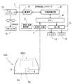
〔撮像画像の処理〕
本願に係る表面欠陥検査装置1にあっては、図4、5に示すように、撮像検査の主要な系統は、上述のように、照射光を被検査面であるバンパー1の塗装面に照明する照明部3と、この照明部3で照明された被検査面を撮像する撮像カメラ4と、この撮像カメラ4からの出力信号を用いた被検査面における欠陥の存在の評価やその評価欠陥の出力を行う画像処理コントローラ5から構成される。
[Processing of captured images]
In the surface
図4、5に示すように、このコントローラ5は、上述のホストコンピュータ14に対する下位コンピュータとして位置されるものであり、この画像処理コントローラ5自体の出力部10に接続される出力機器としてのモニタ12やプリンタ13とを備えている。
As shown in FIGS. 4 and 5, the controller 5 is positioned as a lower computer with respect to the
画像処理コントローラ5には、照明部3の制御を行う照明・撮像制御部9、撮像カメラ4からの出力信号を取り込んでデジタル画像データ(以下単に入力画像と称する)としてメモリ8に展開する画像入力部7、入力画像を用いて欠陥評価を行う欠陥評価手段6を有している。
The image processing controller 5 takes an output signal from the illumination / imaging control unit 9 for controlling the
さらに画像処理コントローラ5は、通信部11を介してホストコンピュータ14にデータ伝送可能に接続されている。
このホストコンピュータ14には必要に応じて画像処理コントローラ5にダウンロードされる検査対象となるバンパー1の情報や搬送装置である搬送ロボット2の動作情報が蓄積され、さらに、画像処理コントローラ5で生成された塗装面の欠陥情報も画像処理コントローラ5からホストコンピュータ14にアップロードされ、そこに蓄積される。
Further, the image processing controller 5 is connected to the
The
また、ホストコンピュータ14にネットワーク接続された端末によって制御される検査結果プロジェクタ15やプリンタなどが目視検査ステーションに備えられ、画像処理コントローラ5からホストコンピュータ14を介して送られてくる欠陥情報に基づいて、検査結果プロジェクタ15を介して欠陥位置などを検査員に指示するように構成されている。
Further, an
上述のように撮像ユニット300は、照明部3の発光面3a及び撮像カメラ4のレンズ面(撮像面に相当)4aは、搬送ロボット2によって搬送されるバンパー1の被検査面に対向して、その照明面3a及び撮像面4aの法線と被検査面の法線とが一致するように、さらに離間距離が一定となるように追従制御される。
As described above, in the
図4に示すように、照明部3は多数の発光素子(この実施形態ではLED素子を用いるので以後LED素子と称することにする)30を、6角形のスペースを残すような網状(リング状)のレイアウトパターンで、しかもこの6角形レイアウトパターンを繰り返すように連続的に(隣接するLED素子30との間をつめながら)配置した構成を有している。6角形網状に配置されたLED素子30によって残されたスペースは、ここでは暗面31と呼ばれ、黒もしくは暗色のプレート面である。
As shown in FIG. 4, the illuminating
網状に配置されたLED素子30によって多くの暗面31が現出しているが、その内の中央軸上に均等分散して位置する暗面31に撮像カメラ4のレンズ面4aが位置されて、複数の撮像カメラ4が照明部3に組み込まれた構成とされている。
Although many
画像処理コントローラ5は、CPUを中核部材として、この表面欠陥検査装置100の種々の動作を行うための機能部をハードウエア又はソフトウエアあるいはその両方で構築している。
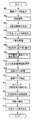
The image processing controller 5 uses a CPU as a core member and constructs a functional unit for performing various operations of the surface
図6に示されているように、本発明に特に関係する機能部として、メモリ8に展開された入力画像を欠陥検出に適した形態に変換する前処理部60Aと、前処理された入力画像を用いて被検査面上の欠陥を見つけ出す欠陥決定部60Bに分けることができる。
As shown in FIG. 6, as a functional unit particularly related to the present invention, a
前処理部60Aは、入力画像に対する輝度調整を行う輝度調整部61と輝度調整された入力画像を2値化処理する2値化処理部62からなる。この実施形態の輝度調整部61は、ガンマ調整だけではなく、入力画像に含まれている発光像の輝度レベルが塗装色や塗装面毎の基準となる正常な被検査面から得られるLED素子の発光像の輝度レベルに達するように画素領域単位の輝度調整も行うように構成されている。
The
また、2値化処理部62は、入力画像の濃淡ヒストグラムから統計的手法で2値化閾値を決定する2値化閾値決定部62aやノイズ消しのために入力画像に対して平滑化フィルタをかけるとともに発光像や欠陥像の輪郭を強調するためにSobelフィルタなどのエッジ強調フィルタをかける画像特徴抽出部62bを備え、2値化閾値決定部62aによって決定された2値化閾値を用いて画像特徴抽出部62bで強調された入力画像を2値化画像にする。
The
2値化処理部62によって2値化された入力画像の一例が図7に示されている。この2値化明暗画像においては、輝度の高い領域は白く表示されているが、6角形レイアウトパターンで連続配置された発光像であるLED素子群は敷き詰められた6角形状の連続して繋がった白い輪郭線として表示され、暗面31に対向する塗装面領域は暗領域として表示され、場合によっては存在する塗装欠陥はその周囲からの照射光による乱反射により暗領域に浮かぶ白い独立した領域として表示される。
An example of the input image binarized by the
このことから、欠陥検出は、2値化画像において、輝度が突出している領域(この実施形態では白い領域)であって所定のパターンで連続していない領域、つまり孤立点を探し出せばよいことになる。所定レベルの輝度値(濃度値)を有しながら連続する画素を探したり、孤立した領域を探したりする画像処理アルゴリズム自体は良く知られたものを用いることができる。 For this reason, in the defect detection, it is only necessary to find an area where luminance is protruding (a white area in this embodiment) and is not continuous in a predetermined pattern, that is, an isolated point in the binarized image. Become. A well-known image processing algorithm for searching for a continuous pixel or an isolated area while having a luminance value (density value) of a predetermined level can be used.
しかしながら、被検査面ここでは塗装面の形状による照射光に対する反射特性の変動等によって、図8に拡大して示すように、本来は連続して繋がった線として現れるLED素子30の発光像に途切れが生じ、その途切れた部分が欠陥として誤検出される可能性がある。このような誤検出を適切に回避するように欠陥決定部60Bは実質的にはプログラムで構成されている。
However, due to the variation of the reflection characteristics with respect to the irradiation light depending on the surface to be inspected here, such as the shape of the painted surface, as shown in an enlarged view in FIG. May occur, and the interrupted portion may be erroneously detected as a defect. The
つまり、この欠陥決定部60Bは、所定数以内の画素数から構成される非連続の独立した画素領域を孤立点として検出して欠陥候補とする欠陥候補抽出部63と、連続配置されたLED素子30の発光像を示す領域に含まれる欠陥候補を欠陥候補から除外する欠陥候補選別部64と、この欠陥候補選別部64で欠陥候補から除外された孤立点領域及び背景などの不要画像領域を統合して欠陥判定対象外領域としてマスク処理する画像マスク生成部65と、画像マスク外に位置する複数の欠陥候補領域を識別するために異なる欠陥候補領域には異なるラベル(番号)を割り当てるラベリング処理を行うラベル設定部66と、各ラベリングされた欠陥候補領域の面積を演算する面積演算部67と、この面積演算部67からの面積情報に基づいて欠陥候補を真の欠陥と判定して欠陥マップに書き込む欠陥判定部68を備えている。
In other words, the
欠陥候補選別部64は、欠陥候補抽出部63で抽出された欠陥候補を選別するために、撮像カメラ4から順次送られてくる画像から所定回数欠陥候補として抽出されているかどうかをチェックすることで突発的に生じる明領域を欠陥候補として認識することを防止する欠陥候補時系列判定部64aと、図8からよく理解できるように抽出された欠陥候補(孤立点)が連続している発光像の延長線上に位置しているからどうかをチェックすることで発光像の途切れ部を欠陥候補として認識することを防止する発光像非連続部探索部64bを備えている。
The defect
この発光像非連続部の探索は、連続する発光像画素を辿っていきながらその途切れ端の延長線領域に位置する暗領域を抽出する形状特徴抽出アルゴリズム等を用いて行うことが可能であり、この途切れ領域に存在する孤立点は欠陥候補から除外される。 This search for the non-continuous portion of the luminescent image can be performed using a shape feature extraction algorithm or the like that extracts a dark region located in the extended line region of the discontinuity while tracing the continuous luminescent image pixels, An isolated point existing in this discontinuous region is excluded from defect candidates.
このように構成された欠陥評価手段6による塗装面の欠陥評価の手順を図9のフローチャートを用いて以下に説明する。 The procedure of the defect evaluation of the painted surface by the defect evaluation means 6 configured as described above will be described below with reference to the flowchart of FIG.
まず、撮像カメラ4から画像入力部7を介して順次送られてくるフレーム画像をメモリ8に取り込む(#01)。取り込まれた入力画像は、輝度調整部61によって輝度(濃度値)調整される(#02)。その際入力画像の特徴量が必要となるが、その特徴量は入力画像を所定の区画数で区画し、各区画毎に演算された濃度平均値の最大値を特徴量とすることが好ましい。
First, the frame images sequentially sent from the
この特徴量は次の2値化閾値の決定は撮像カメラ4のレンズ開口度の調整にも利用できる。2値化閾値決定部62aで2値化閾値が決定されるとともに(#03)、画像特徴抽出部62bで画像の平滑化及びエッジ強調を行った後(#04)、この入力画像は2値化処理されて2値化画像となる(#05)。
This feature amount can be used for the adjustment of the lens aperture of the
2値化された入力画像から、陥候補抽出部63によって、所定数以内(画像解像度等から予め決定される)の画素数からなる孤立した明画素領域が欠陥候補として抽出される(#06)。
From the binarized input image, the fall
抽出された欠陥候補のうち外乱光等により瞬時的かつ局地的に生じる孤立点に属する欠陥候補は欠陥候補時系列判定部64aによって欠陥候補から除外され(#07)、さらに抽出された欠陥候補のうち発光像の途切れ領域に位置する孤立点に属する欠陥候補は発光像非連続部探索部64bによって欠陥候補から除外される(#08)。
Of the extracted defect candidates, defect candidates belonging to isolated points that are instantaneously and locally generated by disturbance light or the like are excluded from the defect candidates by the defect candidate time-
発光像非連続部探索部64bによって見つけ出された発光像の途切れ領域を含むその周辺領域は、ホストコンピュータ14から伝送される被検査物としてのバンパー1の形状情報や搬送ロボット2による搬送位置情報に基づいて決定される被検査面としての塗装面以外の背景領域とともに不要画素領域として画像マスク生成部65によってマスク処理される(#09)。
The peripheral region including the discontinuous region of the light emission image found by the light emission image discontinuous portion searching unit 64b is the shape information of the
なおこの実施形態では、ホストコンピュータ14から得られる搬送位置情報は、実際の位置とは異なる可能があるので、レーザーセンサなどを用いてリアルタイムでのバンパー1の位置ずれをチェックして、その画像マスクの位置を修正している(#10)。
In this embodiment, since the transport position information obtained from the
このようにして欠陥候補の選別や背景画像の除去を終えた後、残されている欠陥候補(孤立点)をラベリングし(#11)、各ラベルを割り当てられた孤立点の面積を演算し(#12)、予め設定されている面積条件(閾値以上の面積をもつかどうか)を満たしている孤立点だけが真の欠陥として判定し(#13)、その座標位置及びサイズなどを欠陥マップに書き込む(#14)。 After selecting defect candidates and removing the background image in this way, the remaining defect candidates (isolated points) are labeled (# 11), and the area of the isolated points to which each label is assigned is calculated ( # 12) Only isolated points satisfying a preset area condition (whether or not having an area equal to or greater than the threshold) are determined as true defects (# 13), and their coordinate positions and sizes are stored in the defect map. Write (# 14).
〔後処理〕
以上で欠陥評価手段6による塗装面の欠陥評価の手順は終了するが、この手順を通じて塗装面の検査が終わると、目視検査ステーション203において、ホストコンピュータ14を介して画像処理コントローラ5から送られてきた欠陥マップのうち、目視検査ステーション203に搬入されたバンパーのIDに一致するIDを付与されている欠陥マップを用いて、欠陥照合が行われる。
[Post-processing]
The procedure of the defect evaluation of the painted surface by the defect evaluation means 6 is completed as described above. When the inspection of the painted surface is completed through this procedure, the image is sent from the image processing controller 5 via the
その際、検査員による照合作業を容易にするため、該当する欠陥マップに基づいて欠陥箇所を指摘するように検査結果プロジェクタ15を動作させると好都合である。もちろん、そのような欠陥マップに基づく欠陥情報を表面欠陥検査装置100の出力部10に接続されたプリンタ13によって紙出力し、この出力用紙をバンパー1に貼り付けてもよい。
At this time, in order to facilitate collation work by the inspector, it is advantageous to operate the
上述した実施形態では、照明部3が6角形の網状に連続配置されたLED素子群で構成されていたが、その網状形態は6角形以外を採用してもよいし、発光素子30としてLED素子以外を採用してもよい。
In the embodiment described above, the illuminating
〔別実施形態〕
上記の実施の形態にあっては、自動車ボディ(特にバンパー)の塗装面の検査を行う例を示したが、検査対象としては任意の表面欠陥を有する被検査面を対象とできる。この種の例としては、プレス形成品の表面検査等がある。
[Another embodiment]
In the above embodiment, an example of inspecting a painted surface of an automobile body (particularly, a bumper) has been shown. However, as an inspection object, an inspection surface having an arbitrary surface defect can be targeted. Examples of this type include surface inspection of press-formed products.
上述した実施形態では、倣いを実行するに最も好ましい倣い状態である、撮像カメラ4の光軸が被検査面の法線方向とされ(倣い条件1)、照明面が被検査面に対して平行で(倣い条件2)、照明面および撮像面が共に、被検査面から所定の距離にある(倣い条件3)関係を満たす倣い装置を示したが、倣いの条件としては、上記倣い条件1〜3のいずれか一つ以上を満たす倣いを行い、他の条件に関しては、画像処理側で処理するようにしてもよい。
In the above-described embodiment, the most preferable copying state for performing copying is that the optical axis of the
上述した実施形態では、欠陥検出のために入力画像を2値化画像に変換していたが、入力画像の2値化に限定されているわけではなく、3値化及びそれ以上の多値化画像を用いて欠陥検出を行うこともできる。 In the above-described embodiment, the input image is converted into a binarized image for defect detection. However, the input image is not limited to binarization, but is not limited to binarization and multilevel binarization. Defect detection can also be performed using an image.
上記の実施形態にあっては、検査システム200を構成するに、ストックステーション202、本願に係る表面欠陥検査装置100、目視検査ステーション203の順に、配置する例を示したが、このシステムを所定の表面加工(塗装、プレス成形等)を伴った製造・検査システムとする場合、ストックステーション、塗装等を実行する加工処理部、表面欠陥検査装置、目視検査ステーションの順に、各工程部を配置することとなる。
In the above embodiment, an example in which the
上記の実施の形態にあっては、発光素子の発光面と、撮像カメラの撮像面とを同一平面上に位置させたが、被検査面からの離間距離で、両面が異なった位置にあってもよい。 In the above embodiment, the light emitting surface of the light emitting element and the imaging surface of the imaging camera are positioned on the same plane, but the two surfaces are at different positions with a distance from the surface to be inspected. Also good.
3:照明部
4:撮像カメラ
5:画像処理コントローラ
6:欠陥評価手段
30:発光素子(LED素子)
31:暗面
60A:前処理部
60B:欠陥決定部
61:輝度調整部
62:2値化処理部
63:欠陥候補(孤立点)抽出部
64:欠陥候補選別部
65:画像マスク生成部
66:ラベル設定部
67:面積演算部
68:欠陥判定部
3: Illumination unit 4: Imaging camera 5: Image processing controller 6: Defect evaluation means 30: Light emitting element (LED element)
31:
Claims (4)
前記レイアウトパターンが前記発光素子を内側に所定形状の暗面を残すように連続的に配置させたものであり、少なくとも一つの前記暗面に前記撮像カメラが前記被検査面から反射される前記各発光素子の照射光を受光するように配置されるとともに、
前記複数の発光素子と前記少なくとも一つの撮像カメラとを一体として前記被検査面に沿って移動させる倣い装置を備えた表面欠陥検査装置。 A plurality of light emitting elements arranged in a predetermined layout pattern, an imaging camera that images a surface to be inspected illuminated by light emitted from the light emitting elements, and an output unit that outputs imaging information of the imaging camera, A surface defect inspection apparatus provided with a defect evaluation unit that evaluates an output signal from an output unit and detects a defect on the surface to be inspected,
The layout pattern is a continuous arrangement of the light emitting elements so as to leave a dark surface of a predetermined shape inside, and the imaging camera is reflected from the surface to be inspected on at least one of the dark surfaces. It is arranged to receive the irradiation light of the light emitting element,
A surface defect inspection apparatus comprising: a copying apparatus that moves the plurality of light emitting elements and the at least one imaging camera integrally along the surface to be inspected.
前記レイアウトパターンの繰り返し方向が前記相対搬送方向である請求項1〜3のいずれか1項記載の表面欠陥検査装置。 A transport mechanism that moves the surface to be inspected relative to the plurality of light emitting elements and the at least one imaging camera;
The surface defect inspection apparatus according to claim 1, wherein a repeating direction of the layout pattern is the relative conveyance direction.
Priority Applications (2)
| Application Number | Priority Date | Filing Date | Title |
|---|---|---|---|
| JP2004105463A JP4318579B2 (en) | 2004-03-31 | 2004-03-31 | Surface defect inspection equipment |
| PCT/JP2004/015467 WO2005100960A1 (en) | 2004-03-31 | 2004-10-20 | Surface defect examining device |
Applications Claiming Priority (1)
| Application Number | Priority Date | Filing Date | Title |
|---|---|---|---|
| JP2004105463A JP4318579B2 (en) | 2004-03-31 | 2004-03-31 | Surface defect inspection equipment |
Publications (2)
| Publication Number | Publication Date |
|---|---|
| JP2005291845A true JP2005291845A (en) | 2005-10-20 |
| JP4318579B2 JP4318579B2 (en) | 2009-08-26 |
Family
ID=35150111
Family Applications (1)
| Application Number | Title | Priority Date | Filing Date |
|---|---|---|---|
| JP2004105463A Expired - Fee Related JP4318579B2 (en) | 2004-03-31 | 2004-03-31 | Surface defect inspection equipment |
Country Status (2)
| Country | Link |
|---|---|
| JP (1) | JP4318579B2 (en) |
| WO (1) | WO2005100960A1 (en) |
Cited By (9)
| Publication number | Priority date | Publication date | Assignee | Title |
|---|---|---|---|---|
| EP1843145A1 (en) | 2006-04-03 | 2007-10-10 | Chuo Electronic Measurement Co., Ltd | Illuminating method in paint defect detecting machine |
| JP2011126643A (en) * | 2009-12-16 | 2011-06-30 | Honda Motor Co Ltd | Bumper conveying device |
| WO2011144964A1 (en) * | 2010-05-17 | 2011-11-24 | Ford Espana S.L. | Inspection system and method of defect detection on specular surfaces |
| JP2014037977A (en) * | 2012-08-10 | 2014-02-27 | Keylex Corp | Press component inspection apparatus |
| JP2014102250A (en) * | 2012-11-16 | 2014-06-05 | Hyundai Motor Company Co Ltd | Vehicular door inspection system and method thereof |
| CN105486248A (en) * | 2015-11-23 | 2016-04-13 | 天津华夏联盛汽车部件有限公司 | Automatic bumper detector |
| JP2016075554A (en) * | 2014-10-06 | 2016-05-12 | 株式会社ディスコ | Wafer inspection method and wafer inspection device |
| CN109239086A (en) * | 2018-10-22 | 2019-01-18 | 上海爱被思智能科技有限公司 | Vehicle paint and appearance defect detection system |
| JP2020003228A (en) * | 2018-06-25 | 2020-01-09 | 株式会社キーレックス | Press component inspection device and press component inspection method |
Families Citing this family (3)
| Publication number | Priority date | Publication date | Assignee | Title |
|---|---|---|---|---|
| CA2684365A1 (en) | 2007-04-16 | 2008-10-23 | Josep Maria Tornero Montserrat | System of detection of faults in surfaces by merging of images by means of light sweeping |
| JP6984747B2 (en) * | 2018-06-05 | 2021-12-22 | 日本電気株式会社 | Displacement measuring device, displacement measuring method, and program |
| CN114486929B (en) * | 2022-01-20 | 2024-02-02 | 深圳佳视德智能科技有限公司 | Automobile door trim appearance detection method and device |
Family Cites Families (5)
| Publication number | Priority date | Publication date | Assignee | Title |
|---|---|---|---|---|
| JPS54134485A (en) * | 1978-04-10 | 1979-10-18 | Hitachi Ltd | Applying and wiping device of liquid to and from test piece |
| JP3058777B2 (en) * | 1993-02-19 | 2000-07-04 | 関東自動車工業株式会社 | Paint surface inspection method and apparatus using image signal |
| JP2000136917A (en) * | 1998-10-30 | 2000-05-16 | Moritex Corp | Method for observing surface of molded article and lighting device used therefor |
| JP2000321037A (en) * | 1999-05-14 | 2000-11-24 | Nissan Motor Co Ltd | Surface defect quantitative evaluation method and device |
| JP3757694B2 (en) * | 1999-08-25 | 2006-03-22 | トヨタ自動車株式会社 | Surface defect inspection method |
-
2004
- 2004-03-31 JP JP2004105463A patent/JP4318579B2/en not_active Expired - Fee Related
- 2004-10-20 WO PCT/JP2004/015467 patent/WO2005100960A1/en not_active Ceased
Cited By (13)
| Publication number | Priority date | Publication date | Assignee | Title |
|---|---|---|---|---|
| EP1843145A1 (en) | 2006-04-03 | 2007-10-10 | Chuo Electronic Measurement Co., Ltd | Illuminating method in paint defect detecting machine |
| JP2011126643A (en) * | 2009-12-16 | 2011-06-30 | Honda Motor Co Ltd | Bumper conveying device |
| WO2011144964A1 (en) * | 2010-05-17 | 2011-11-24 | Ford Espana S.L. | Inspection system and method of defect detection on specular surfaces |
| JP2014037977A (en) * | 2012-08-10 | 2014-02-27 | Keylex Corp | Press component inspection apparatus |
| US10393673B2 (en) | 2012-11-16 | 2019-08-27 | Hyundai Motor Company | Door inspection system for vehicle and inspection method for the same |
| JP2014102250A (en) * | 2012-11-16 | 2014-06-05 | Hyundai Motor Company Co Ltd | Vehicular door inspection system and method thereof |
| JP2016075554A (en) * | 2014-10-06 | 2016-05-12 | 株式会社ディスコ | Wafer inspection method and wafer inspection device |
| CN105486248A (en) * | 2015-11-23 | 2016-04-13 | 天津华夏联盛汽车部件有限公司 | Automatic bumper detector |
| CN105486248B (en) * | 2015-11-23 | 2017-11-28 | 天津华夏联盛汽车部件有限公司 | A kind of bumper self-checking device |
| JP2020003228A (en) * | 2018-06-25 | 2020-01-09 | 株式会社キーレックス | Press component inspection device and press component inspection method |
| JP7254327B2 (en) | 2018-06-25 | 2023-04-10 | 株式会社キーレックス | PRESS PARTS INSPECTION DEVICE AND PRESS PARTS INSPECTION METHOD |
| CN109239086A (en) * | 2018-10-22 | 2019-01-18 | 上海爱被思智能科技有限公司 | Vehicle paint and appearance defect detection system |
| CN109239086B (en) * | 2018-10-22 | 2023-11-17 | 上海易清智觉自动化科技有限公司 | Vehicle paint surface and appearance flaw detection system |
Also Published As
| Publication number | Publication date |
|---|---|
| WO2005100960A1 (en) | 2005-10-27 |
| JP4318579B2 (en) | 2009-08-26 |
Similar Documents
| Publication | Publication Date | Title |
|---|---|---|
| KR100742003B1 (en) | Surface defect inspecting method and device | |
| CN111272763B (en) | System and method for workpiece inspection | |
| US8050486B2 (en) | System and method for identifying a feature of a workpiece | |
| EP3388781B1 (en) | System and method for detecting defects in specular or semi-specular surfaces by means of photogrammetric projection | |
| EP3060899B1 (en) | Method and device for tyre condition analysis | |
| JP6264132B2 (en) | Inspection device and inspection method for painted surface of vehicle body | |
| CN111220582A (en) | Fluorescence penetrant inspection system and method | |
| JP4318579B2 (en) | Surface defect inspection equipment | |
| CN100520376C (en) | Surface defect inspection method and device | |
| CN109693140A (en) | A kind of intelligent flexible production line and its working method | |
| JP2000193601A (en) | Surface defect inspection equipment | |
| JP4322230B2 (en) | Surface defect inspection apparatus and surface defect inspection method | |
| CN105572133B (en) | Flaw detection method and device | |
| JP4349960B2 (en) | Surface defect inspection equipment | |
| JP2005214720A (en) | Surface inspection device and surface inspection method | |
| JP2005315841A (en) | Surface defect inspection device | |
| JP2007316019A (en) | Surface defect inspection device | |
| JP4315899B2 (en) | Surface inspection method and surface inspection apparatus | |
| KR20260005988A (en) | Inspection device for surface coating | |
| JP4371883B2 (en) | Illumination light source unit for inspection and surface defect inspection apparatus using the light source unit | |
| KR101555580B1 (en) | Inspecting apparatus for huge plane | |
| JP4017585B2 (en) | Paint surface inspection equipment | |
| CN111833350A (en) | Machine vision detection method and system | |
| JP4016381B2 (en) | Surface defect inspection equipment | |
| US20240310291A1 (en) | Device for automatic vehicle body damage detection |
Legal Events
| Date | Code | Title | Description |
|---|---|---|---|
| A621 | Written request for application examination |
Free format text: JAPANESE INTERMEDIATE CODE: A621 Effective date: 20061208 |
|
| A131 | Notification of reasons for refusal |
Free format text: JAPANESE INTERMEDIATE CODE: A131 Effective date: 20080828 |
|
| A521 | Written amendment |
Free format text: JAPANESE INTERMEDIATE CODE: A523 Effective date: 20081006 |
|
| A131 | Notification of reasons for refusal |
Free format text: JAPANESE INTERMEDIATE CODE: A131 Effective date: 20090205 |
|
| A521 | Written amendment |
Free format text: JAPANESE INTERMEDIATE CODE: A523 Effective date: 20090401 |
|
| TRDD | Decision of grant or rejection written | ||
| A01 | Written decision to grant a patent or to grant a registration (utility model) |
Free format text: JAPANESE INTERMEDIATE CODE: A01 Effective date: 20090514 |
|
| A01 | Written decision to grant a patent or to grant a registration (utility model) |
Free format text: JAPANESE INTERMEDIATE CODE: A01 |
|
| A61 | First payment of annual fees (during grant procedure) |
Free format text: JAPANESE INTERMEDIATE CODE: A61 Effective date: 20090526 |
|
| FPAY | Renewal fee payment (event date is renewal date of database) |
Free format text: PAYMENT UNTIL: 20120605 Year of fee payment: 3 |
|
| R150 | Certificate of patent or registration of utility model |
Free format text: JAPANESE INTERMEDIATE CODE: R150 |
|
| FPAY | Renewal fee payment (event date is renewal date of database) |
Free format text: PAYMENT UNTIL: 20140605 Year of fee payment: 5 |
|
| R250 | Receipt of annual fees |
Free format text: JAPANESE INTERMEDIATE CODE: R250 |
|
| LAPS | Cancellation because of no payment of annual fees |