JP2005290435A - Pin for chain and production method therefor - Google Patents
Pin for chain and production method therefor Download PDFInfo
- Publication number
- JP2005290435A JP2005290435A JP2004104572A JP2004104572A JP2005290435A JP 2005290435 A JP2005290435 A JP 2005290435A JP 2004104572 A JP2004104572 A JP 2004104572A JP 2004104572 A JP2004104572 A JP 2004104572A JP 2005290435 A JP2005290435 A JP 2005290435A
- Authority
- JP
- Japan
- Prior art keywords
- layer
- pin
- chain
- treatment
- base material
- Prior art date
- Legal status (The legal status is an assumption and is not a legal conclusion. Google has not performed a legal analysis and makes no representation as to the accuracy of the status listed.)
- Pending
Links
Images

Abstract
Description
本発明は、耐摩耗性を向上させたチェーン用ピンおよびその製造方法に関する。 The present invention relates to a chain pin with improved wear resistance and a method for manufacturing the same.
サイレントチェーンやローラチェーン等の動力伝達用チェーンやプライマリドライブチェーンにおいては、チェーンの運転中にリンクがピンの回りを回転摺動することによってピンが摩耗する。そこで、従来よりピンの耐摩耗性を向上させるための種々の硬化処理が提案されている。 In a power transmission chain such as a silent chain or a roller chain or a primary drive chain, the link wears as the link rotates and slides around the pin during operation of the chain. Therefore, various hardening treatments for improving the wear resistance of the pins have been proposed.
たとえば、特開平10−169723号公報に示すものでは、ピン素材の表面にクロム、チタニウム、バナジウム、ニオビウムのうちの少なくとも一つの炭化物層を形成している。 For example, in the one disclosed in Japanese Patent Laid-Open No. 10-169723, at least one carbide layer of chromium, titanium, vanadium, and niobium is formed on the surface of the pin material.
ここで、本件出願に係る発明者らは、チェーン用ピンに種々の条件下でバナダイズ処理(VC処理)を行ってピン表面にバナジウム炭化物層(VC層)を形成し、このようなVC処理を行った各種VCピンをそれぞれチェーンに組み込んで、各チェーンに対してそれぞれ摩耗試験を行った。その結果、VC層の違いにより、チェーン摩耗伸びにばらつきが生じることが分かった。 Here, the inventors of the present application perform vanadium treatment (VC treatment) on the chain pin under various conditions to form a vanadium carbide layer (VC layer) on the surface of the pin, and perform such VC treatment. Each of the various VC pins performed was incorporated into a chain, and each chain was subjected to a wear test. As a result, it was found that the chain wear elongation varies depending on the VC layer.
そこで、各VC層をX線線分析法により元素分析した結果、以下のことが判明した。すなわち、バナジウム炭化物の中で耐摩耗性にもっとも優れているのは、V8C7であり、これ以外のバナジウム炭化物を多く含む不純物層は、V8C7に比べて耐摩耗性に劣ることが分かった。また、不純物層は、VC処理の炉内冷却時に形成されると考えられ、V2Cを多く含むと推測されているが、ピンの最表部に形成されることが多いこともわかった。
本発明は、このような検証結果に基づいてなされたもので、本発明が解決しようとする課題は、耐摩耗性を向上させることができるチェーン用ピンおよびその製造方法を提供することにある。 The present invention has been made on the basis of such verification results, and a problem to be solved by the present invention is to provide a chain pin capable of improving wear resistance and a method for manufacturing the same.
請求項1の発明に係るチェーン用ピンは、チェーン用ピンの母材となる鋼の最表部に、不純物層が除去されたVC層が形成されていることを特徴としている。
The chain pin according to the invention of
請求項2の発明に係るチェーン用ピンは、チェーン用ピンの母材となる鋼の最表部に、V8 C7 以外のバナジウム炭化物を多く含む不純物層が除去されたVC層が形成されていることを特徴としている。
In the chain pin according to the invention of
請求項3の発明に係るチェーン用ピンは、チェーン用ピンの母材となる鋼の最表部に、V8C7を含みかつV2Cが除去されたVC層が形成されていることを特徴としている。
In the chain pin according to the invention of
請求項4の発明に係るチェーン用ピンは、請求項1ないし3のいずれかにおいて、VC層が、CrCまたはCrが混合された混合層であることを特徴としている。 A chain pin according to a fourth aspect of the present invention is characterized in that, in any one of the first to third aspects, the VC layer is a mixed layer in which CrC or Cr is mixed.
請求項5の発明に係るチェーン用ピンは、請求項1ないし4のいずれかにおいて、VC層と母材との間の境界領域において、V8C7の含有率が急激に減少しかつCrCの含有率が急激に増加している境界層が形成されていることを特徴としている。 A chain pin according to a fifth aspect of the present invention is the chain pin according to any one of the first to fourth aspects, wherein the content of V 8 C 7 is drastically decreased in the boundary region between the VC layer and the base material, and CrC It is characterized by the formation of a boundary layer with a rapidly increasing content.
請求項6の発明に係るチェーン用ピンは、請求項1ないし3のいずれかにおいて、不純物層またはV2Cがいずれも研磨処理によって除去されていることを特徴としている。 A chain pin according to a sixth aspect of the present invention is characterized in that, in any one of the first to third aspects, the impurity layer or V 2 C is removed by a polishing process.
請求項7の発明に係るチェーン用ピンの製造方法は、以下の工程から構成されている。
i)チェーン用ピンの母材となる鋼の表面に、バナダイズ処理を行うことにより、V8C7を含むVC層を形成させる。
ii)研磨処理により、VC層の最表層から不純物層を除去する。
The manufacturing method of the pin for chains concerning the invention of Claim 7 is comprised from the following processes.
i) A VC layer containing V 8 C 7 is formed on the surface of the steel serving as the base material of the chain pin by vanadizing.
ii) The impurity layer is removed from the outermost layer of the VC layer by polishing treatment.
請求項8の発明に係るチェーン用ピンの製造方法は、以下の工程から構成されている。
i)チェーン用ピンの母材となる鋼の表面に、バナダイズ処理を行うことにより、V8C7を含むVC層を形成させる。
ii)研磨処理により、VC層の最表層からV2Cを除去する。
The chain pin manufacturing method according to the invention of claim 8 includes the following steps.
i) A VC layer containing V 8 C 7 is formed on the surface of the steel serving as the base material of the chain pin by vanadizing.
ii) V 2 C is removed from the outermost layer of the VC layer by a polishing process.
請求項9の発明に係るチェーン用ピンの製造方法は、以下の工程から構成されている。
i)チェーン用ピンの母材となる鋼の表面に、クロマイジング処理を行うことによりCrC層を形成させる。
ii)クロマイジング処理の際の温度よりも高温でクロマイジングおよびバナダイズ処理を行うことにより、V8C7を含むバナジウム炭化物およびクロム炭化物の混合層をCrC層の上に形成させる。
iii)研磨処理により、混合層の最表層から不純物層を除去する。
The manufacturing method of the chain pin which concerns on invention of Claim 9 is comprised from the following processes.
i) A CrC layer is formed on the surface of the steel used as the base material of the chain pin by performing chromizing treatment.
ii) A mixed layer of vanadium carbide and chromium carbide containing V 8 C 7 is formed on the CrC layer by performing chromizing and vanadium treatment at a temperature higher than that in the chromizing treatment.
iii) The impurity layer is removed from the outermost layer of the mixed layer by polishing treatment.
請求項10の発明に係るチェーン用ピンの製造方法は、以下の工程から構成されている。
i)チェーン用ピンの母材となる鋼の表面に、クロマイジング処理を行うことによりCrC層を形成させる。
ii)クロマイジング処理の際の温度よりも高温でクロマイジングおよびバナダイズ処理を行うことにより、V8C7を含むバナジウム炭化物およびクロム炭化物の混合層をCrC層の上に形成させる。
iii)研磨処理により、混合層の最表層からV2Cを除去する。
The manufacturing method of the chain pin which concerns on invention of
i) A CrC layer is formed on the surface of the steel used as the base material of the chain pin by performing chromizing treatment.
ii) A mixed layer of vanadium carbide and chromium carbide containing V 8 C 7 is formed on the CrC layer by performing chromizing and vanadium treatment at a temperature higher than that in the chromizing treatment.
iii) V 2 C is removed from the outermost layer of the mixed layer by polishing treatment.
請求項11の発明に係るチェーン用ピンの製造方法は、請求項7ないし10のいずれかにおいて、最表層から除去される層の厚みが2〜5μmであることを特徴としている。 The method for manufacturing a chain pin according to the invention of claim 11 is characterized in that, in any of claims 7 to 10, the thickness of the layer removed from the outermost layer is 2 to 5 μm.
請求項12の発明に係るチェーン用ピンの製造方法は、請求項7ないし10のいずれかにおいて、研磨処理が、ビッカース硬度Hv2000〜5500の研磨剤を用いたバレル研磨処理であることを特徴としている。 A chain pin manufacturing method according to a twelfth aspect of the invention is characterized in that, in any of the seventh to tenth aspects, the polishing treatment is a barrel polishing treatment using an abrasive having a Vickers hardness of Hv 2000 to 5500. .
請求項13の発明に係るチェーン用ピンは、請求項7ないし12のいずれかの方法により製造されている。 A chain pin according to a thirteenth aspect of the present invention is manufactured by any one of the seventh to twelfth methods.
本発明によれば、チェーン用ピンの母材となる鋼の最表部に、不純物層が除去されたVC層を形成するようにしたので、ピンの耐摩耗性を向上させることができる。 According to the present invention, since the VC layer from which the impurity layer has been removed is formed on the outermost surface portion of the steel serving as the base material of the chain pin, the wear resistance of the pin can be improved.
以下、本発明の実施態様を添付図面に基づいて説明する。
<第1の実施例>
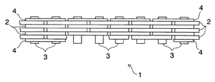
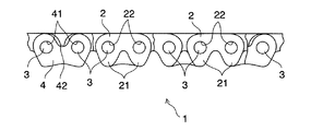
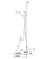
図1は本発明の第1の実施例による連結ピンが採用されたサイレントチェーンの平面概略図、図2はその正面概略図、図3(a)は研磨処理前の連結ピンの断面部分図、同図(b)は研磨処理後の連結ピンの断面部分図、図4は連結ピンのVC処理の際の温度制御線図、図5はサイレントチェーンの摩耗試験後の連結ピンおよびリンクプレートの摩耗量を示すグラフである。
Embodiments of the present invention will be described below with reference to the accompanying drawings.
<First embodiment>
FIG. 1 is a schematic plan view of a silent chain employing a connection pin according to a first embodiment of the present invention, FIG. 2 is a schematic front view thereof, FIG. 3A is a partial sectional view of the connection pin before polishing, FIG. 4B is a partial sectional view of the connecting pin after the polishing process, FIG. 4 is a temperature control diagram for the VC processing of the connecting pin, and FIG. 5 is the wear of the connecting pin and the link plate after the silent chain wear test. It is a graph which shows quantity.
図1および図2に示すように、サイレントチェーン1は、各々一対の歯部21およびピン穴22を有する多数のリンクプレート2を厚み方向および長手方向に積層するとともに、各ピン穴22内に挿入した連結ピン(チェーン用ピン)3で各リンクプレート2を枢支可能に連結することにより構成されている。リンクプレート2の最外側には、ガイドリンク4が配置されており、ガイドリンク4のピン穴41内には、連結ピン3の端部が固定されている。なお、ここでは、ガイドリンクとして、その背面側にクロッチ部42が形成されたいわゆる低剛性ガイドを例にとっている。
As shown in FIGS. 1 and 2, the
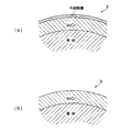
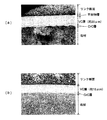
連結ピン3には、VC処理(バナダイズ処理)による硬化処理が施されており、VC処理後、連結ピン3の母材表面には、図3(a)に示すように、V8C7を主成分とするバナジウム炭化物層(VC層)が形成されており、VC層の上の最表層には、不純物層が形成されている。VC処理後、連結ピン3には、バレル研磨などの研磨処理が施されており、これにより、図3(b)に示すように、最表層の不純物層が除去されている。不純物層は、V8C7以外のバナジウム炭化物を多く含む層であり、主にV2Cを含んでいると推測される。また、バレル研磨により除去される不純物層の厚みは、2〜5μmが好ましい。
The connecting
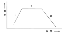
次に、連結ピン3のVC処理について、図4を用いて説明する。図4は、ピンの加熱処理炉(図示せず)の温度制御を説明するための線図であり、この温度分布はI,II, III の3つの部分から構成されている。
Next, the VC processing of the connecting
まず、図4中のIに示すように、炉内の温度を900〜1100℃まで上昇させる。そして、IIに示すように、炉内の温度を所定時間一定に保持する。このとき、炉内においてピン母材の表層では、以下の反応が進行していると考えられる。
8VCl2+7C ⇔ V8C7↓+8Cl2
First, as shown by I in FIG. 4, the temperature in the furnace is raised to 900 to 1100 ° C. Then, as shown in II, the temperature in the furnace is kept constant for a predetermined time. At this time, it is considered that the following reaction proceeds in the surface layer of the pin base material in the furnace.
8VCl 2 + 7C V V 8 C 7 ↓ + 8Cl 2
次に、III に示すように、炉内の温度を下げる。このとき、炉内においてピン母材の表層では、以下の反応が進行していると考えられる。
2VCl2+C ⇔ V2C↓+2Cl2
Next, as shown in III, the temperature in the furnace is lowered. At this time, it is considered that the following reaction proceeds in the surface layer of the pin base material in the furnace.
2VCl 2 + C ⇔ V 2 C ↓ +
このようにして、連結ピンの母材の上にV8C7からなるバナジウム炭化物層(VC層)が形成されるとともに、その表層に、V8C7以外のバナジウム炭化物を多く含む不純物層が形成されることになる(図3(a)参照)。 In this way, a vanadium carbide layer (VC layer) made of V 8 C 7 is formed on the base material of the connecting pin, and an impurity layer containing a large amount of vanadium carbide other than V 8 C 7 is formed on the surface layer. It will be formed (see FIG. 3A).
ところで、連結ピンのVC処理の際に、最表層に不純物層が形成されるのは、図4中のIII に示すような炉内冷却時に、連結ピンの母材からのC原子の供給が減少するためであると考えられる。 By the way, during the VC treatment of the connecting pin, the impurity layer is formed in the outermost layer because the supply of C atoms from the base material of the connecting pin is reduced during the furnace cooling as indicated by III in FIG. It is thought that it is to do.
次に、連結ピンに対して、バレル研磨処理を施すことにより、連結ピンの最表層の不純物層を除去する。このバレル研磨処理の際には、ビッカース硬度Hv2000〜5500の研磨剤を用いて処理するのが好ましい。これは、連結ピンの母材表面に形成されるV8C7の硬度がHv2500程度であり、また最表層の不純物層の硬度がHv2000程度かまたはこれよりも低いためである。 Next, the outermost impurity layer of the connecting pin is removed by subjecting the connecting pin to barrel polishing. In the barrel polishing process, it is preferable to use an abrasive having a Vickers hardness of Hv 2000 to 5500. This is because the hardness of V 8 C 7 formed on the surface of the base material of the connecting pin is about Hv 2500, and the hardness of the outermost impurity layer is about Hv 2000 or lower.
このようなバレル研磨処理により、図3(b)に示すように、連結ピンの母材表面には、V8C7のみからなるバナジウム炭化物層(VC層)が残ることになる。 By such barrel polishing treatment, as shown in FIG. 3B, a vanadium carbide layer (VC layer) made of only V 8 C 7 remains on the surface of the base material of the connecting pin.
次に、不純物層が除去された連結ピンからなるサイレントチェーンと、不純物層が残されたままの連結ピンからなるサイレントチェーンの双方について、同様の条件下で摩耗試験を行った。試験条件は、以下のとおりである。
ドライブスプロケット回転数:6000rpm
潤滑方法:強制給油(0.5L/min)
運転時間:100時間
Next, a wear test was performed under the same conditions for both the silent chain composed of the connecting pin from which the impurity layer was removed and the silent chain composed of the connecting pin with the impurity layer remaining. The test conditions are as follows.
Drive sprocket rotation speed: 6000rpm
Lubrication method: Forced lubrication (0.5 L / min)
Operating time: 100 hours
摩耗試験結果を図5に示す。同図において、連結ピンの不純物層が除去されたサイレントチェーンの摩耗試験結果を右側の棒グラフで、連結ピンに不純物層が残されたままのサイレントチェーンの摩耗試験結果を左側の棒グラフでそれぞれ示している。また、各棒グラフにおいて、白抜きの部分はチェーン1ピッチ当たりのリンク摩耗量を示し、網かけの部分はチェーン1ピッチ当たりのピン摩耗量を示している。 The results of the wear test are shown in FIG. In the same figure, the wear test results of the silent chain with the impurity layer of the connecting pin removed are shown on the right bar graph, and the wear test results of the silent chain with the impurity layer remaining on the connecting pin are shown on the left bar graph. Yes. In each bar graph, the white portions indicate the amount of link wear per chain pitch, and the shaded portions indicate the amount of pin wear per chain pitch.
図5から分かるように、連結ピンに不純物層が残されたものでは、リンクプレートの摩耗量が8μmで、ピンの摩耗量が0.6μmであった。また、連結ピンの不純物層が除去されたものでは、リンクプレートの摩耗量が4μmで、ピンの摩耗量が0.3μmであった。 As can be seen from FIG. 5, when the impurity layer was left on the connecting pin, the wear amount of the link plate was 8 μm and the wear amount of the pin was 0.6 μm. In the case where the impurity layer of the connecting pin was removed, the wear amount of the link plate was 4 μm and the wear amount of the pin was 0.3 μm.
このように、不純物層が除去されたサイレントチェーンの方が、連結ピンの摩耗量のみならず、リンクプレートのピン穴の摩耗量も著しく低下していることが分かる。 Thus, it can be seen that in the silent chain from which the impurity layer is removed, not only the wear amount of the connecting pin but also the wear amount of the pin hole of the link plate is significantly reduced.
<第2の実施例>
第1の実施例では、連結ピンの母材表面に、バナジウム炭化物のみからなるVC層が形成された例を示したが、本発明の適用はこれに限定されない。VC層の内部にクロムまたはクロム炭化物(CrC)が混合されていてもよい。
<Second embodiment>
In the first embodiment, an example in which a VC layer made only of vanadium carbide is formed on the surface of the base material of the connecting pin is shown, but the application of the present invention is not limited to this. Chromium or chromium carbide (CrC) may be mixed inside the VC layer.
図6は、このような硬化層が形成された連結ピンの母材表面の断面写真を示しており、同図(a)は研磨処理前の連結ピンの断面拡大部分図、同図(b)は研磨処理後の連結ピンの断面拡大部分図である。なお、図6においては、連結ピンがガイドリンクに固定された状態で示されており、このため、ピン断面の上方には、ガイドリンク断面が併せて示されている。 FIG. 6 shows a cross-sectional photograph of the surface of the base material of the connecting pin on which such a hardened layer is formed. FIG. 6 (a) is an enlarged partial sectional view of the connecting pin before polishing, and FIG. 6 (b). FIG. 4 is an enlarged partial sectional view of a connecting pin after polishing treatment. In FIG. 6, the connecting pin is shown fixed to the guide link. For this reason, the guide link cross section is also shown above the pin cross section.
連結ピン3には、クロム浸透処理(クロマイジング処理)およびVC処理(バナダイズ処理)による硬化処理が施されている。硬化処理後、連結ピン3の母材表面には、図6(a)に示すように、CrC層と、その上層に配置されたVC層とが形成されており、VC層の最表層には、不純物層が形成されている。硬化処理後、連結ピン3には、バレル研磨などの研磨処理が施されており、これにより、図6(b)に示すように、最表層の不純物層が除去されている。なお、このバレル研磨では、VC層が5μmほど除去されている。不純物層は、上述したように、V8C7以外のバナジウム炭化物を多く含む層であり、主にV2Cを含んでいると推測される。
The connecting
連結ピン3の母材表面の組成をさらに詳細に示したのが図7である。同図は、波長分散型X線マイクロアナライザによるX線線分析法により元素分析された結果を示している。同図に示すように、連結ピン3の硬化層は、母材の最表面に形成され、VCを主成分としかつ少量のCrCを含む炭化物層と、炭化物層および母材間に形成され、VC(正確にはV8C7)の含有率が急激に減少しかつCrCの含有率が急激に増加している境界層とから構成されている。
FIG. 7 shows the composition of the surface of the base material of the connecting
このような連結ピンの硬化処理方法について説明すると、以下のとおりである。
まず、第1の工程において、チェーン用ピンの母材となる鋼である、たとえば軸受鋼や機械構造用炭素鋼に対して、800〜900℃の温度下でクロム浸透処理を行うことにより、数μm程度の厚みの薄いクロム炭化物層を鋼の表面に形成させる。
A description will be given of such a curing method for the connecting pin as follows.
First, in the first step, by performing chromium infiltration treatment at a temperature of 800 to 900 ° C., for example, bearing steel or carbon steel for mechanical structure, which is a steel used as a base material for a chain pin, several A thin chromium carbide layer having a thickness of about μm is formed on the steel surface.
その後、第2の工程において、900〜1100℃の温度下で、クロムおよびバナジウム浸透処理を行うことにより、鋼の最表面に、すなわち第1の工程で形成されたクロム炭化物層の上に、バナジウム炭化物およびクロム炭化物の混合層を形成させる。この混合層の形成時には、第1の工程で形成されたクロム炭化物層の内部に徐々にバナジウム炭化物層が浸透していくことになる。このクロムおよびバナジウム浸透処理は、第1の工程におけるクロム浸透処理よりも長時間にわたって実行される。これにより、クロムよりもバナジウムを多く含みかつクロム炭化物層よりも厚い炭化物層(V8C7層)が鋼の表面に形成される。また、このとき、最表層には、V8C7以外のバナジウム炭化物を多く含む不純物層が形成される。 Thereafter, in the second step, vanadium is formed on the outermost surface of the steel, that is, on the chromium carbide layer formed in the first step, by performing chromium and vanadium permeation treatment at a temperature of 900 to 1100 ° C. A mixed layer of carbide and chromium carbide is formed. When this mixed layer is formed, the vanadium carbide layer gradually penetrates into the chromium carbide layer formed in the first step. This chromium and vanadium infiltration treatment is performed for a longer time than the chromium infiltration treatment in the first step. As a result, a carbide layer (V 8 C 7 layer) that contains more vanadium than chromium and is thicker than the chromium carbide layer is formed on the surface of the steel. At this time, an impurity layer containing a large amount of vanadium carbide other than V 8 C 7 is formed in the outermost layer.
その一方、第2の工程でのクロムおよびバナジウム浸透処理に先立って、第1の工程でクロムの浸透処理が行われているので、鋼の最表面に形成されたバナジウム炭化物およびクロム炭化物の混合層と鋼との間の境界領域には、クロム炭化物を比較的多量に含むクロムリッチ層が形成されることになる。 On the other hand, since chromium penetration treatment is performed in the first step prior to chromium and vanadium penetration treatment in the second step, a mixed layer of vanadium carbide and chromium carbide formed on the outermost surface of the steel A chromium-rich layer containing a relatively large amount of chromium carbide is formed in the boundary region between the steel and the steel.
次に、連結ピンに対して、ビッカース硬度Hv2000〜5500の研磨剤を用いてバレル研磨処理を施すことにより、連結ピンの最表層の不純物層を除去する。このバレル研磨処理により、前記第1の実施例と同様に、連結ピンの母材表面には、CrCを含むVC層のみが残ることになる(図6(b))。 Next, the outermost impurity layer of the connecting pin is removed by subjecting the connecting pin to barrel polishing using an abrasive having a Vickers hardness of Hv 2000 to 5500. As a result of this barrel polishing process, only the VC layer containing CrC remains on the surface of the base material of the connecting pin, as in the first embodiment (FIG. 6B).
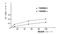
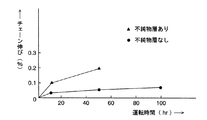
次に、不純物層が除去された連結ピンからなるサイレントチェーンと、不純物層が残されたままの連結ピンからなるサイレントチェーンの双方について、同様の条件下で摩耗試験を行った結果を図8および図9に示す。図8は、潤滑油として未使用のクリーンオイルを使用した場合の試験結果を示し、図9は、潤滑油として添加剤入りのオイルを使用した場合の試験結果を示している。 Next, FIG. 8 and FIG. 8 show the results of a wear test performed under the same conditions for both the silent chain composed of the connecting pin from which the impurity layer has been removed and the silent chain composed of the connecting pin with the impurity layer remaining. As shown in FIG. FIG. 8 shows a test result when unused clean oil is used as the lubricating oil, and FIG. 9 shows a test result when oil containing an additive is used as the lubricating oil.
図8および図9から明らかなように、いずれのオイルを用いた場合でも、不純物層が除去されたサイレントチェーンの方が、チェーン伸びが低下しており、このことから、不純物層が除去されている連結ピンの方が耐摩耗性が向上していることが分かる。 As is clear from FIG. 8 and FIG. 9, in any oil, the chain elongation is lower in the silent chain from which the impurity layer is removed, and from this, the impurity layer is removed. It can be seen that the wear resistance of the connecting pin is improved.
しかも、この場合には、母材およびバナジウム炭化物との結合力が大きいクロム炭化物を比較的多く含むクロムリッチ層が炭化物層と母材との間の境界層に形成されることにより、高面圧下でも炭化物層が母材から剥離しにくくなっており、これにより、ピンの耐摩耗性が一層向上している。 Moreover, in this case, a chromium-rich layer containing a relatively large amount of chromium carbide having a high bonding strength with the base material and vanadium carbide is formed in the boundary layer between the carbide layer and the base material, thereby reducing the high surface pressure. However, the carbide layer is difficult to peel off from the base material, which further improves the wear resistance of the pin.
<他の実施例>
前記各実施例では、硬化処理後の連結ピンの研磨処理として、バレル研磨を例にとって説明したが、本発明の適用はこれに限定されない。たとえば、センタレス研磨により研磨処理を行うようにしてもよい。
<Other embodiments>
In each of the above-described embodiments, barrel polishing has been described as an example of the polishing process for the connecting pins after the curing process, but the application of the present invention is not limited thereto. For example, the polishing process may be performed by centerless polishing.
1: サイレントチェーン
3: 連結ピン(チェーン用ピン)
1: Silent chain 3: Connecting pin (pin for chain)
Claims (13)
ことを特徴とするチェーン用ピン。 A VC layer from which the impurity layer has been removed is formed on the outermost surface of the steel that is the base material of the chain pin.
A pin for a chain characterized by that.
ことを特徴とするチェーン用ピン。 A VC layer from which an impurity layer containing a large amount of vanadium carbide other than V 8 C 7 is removed is formed on the outermost surface of the steel that is the base material of the chain pin.
A pin for a chain characterized by that.
ことを特徴とするチェーン用ピン。 A VC layer that includes V 8 C 7 and from which V 2 C is removed is formed on the outermost surface of the steel that is the base material of the chain pin.
A pin for a chain characterized by that.
前記VC層は、CrCまたはCrが混合された混合層である、
ことを特徴とするチェーン用ピン。 In any of claims 1 to 3,
The VC layer is a mixed layer in which CrC or Cr is mixed.
A pin for a chain characterized by that.
前記VC層と前記母材との間の境界領域において、V8C7の含有率が急激に減少しかつCrCの含有率が急激に増加している境界層が形成されている、
ことを特徴とするチェーン用ピン。 In any of claims 1 to 4,
In the boundary region between the VC layer and the base material, a boundary layer is formed in which the content rate of V 8 C 7 is rapidly decreased and the content rate of CrC is rapidly increased.
A pin for a chain characterized by that.
前記不純物層または前記V2Cがいずれも研磨処理によって除去されている、
ことを特徴とするチェーン用ピン。 In any of claims 1 to 3,
The impurity layer or the V 2 C is both removed by a polishing process.
A pin for a chain characterized by that.
チェーン用ピンの母材となる鋼の表面に、バナダイズ処理を行うことにより、V8C7を含むVC層を形成させ、
次に、研磨処理により、前記VC層の最表層から不純物層を除去した、
ことを特徴とするチェーン用ピンの製造方法。 A method of manufacturing a pin for a chain,
By performing vanadizing treatment on the surface of the steel that is the base material of the chain pin, a VC layer containing V 8 C 7 is formed,
Next, the impurity layer was removed from the outermost layer of the VC layer by polishing treatment.
A method for manufacturing a pin for a chain, characterized in that:
チェーン用ピンの母材となる鋼の表面に、バナダイズ処理を行うことにより、V8C7を含むVC層を形成させ、
次に、研磨処理により、前記VC層の最表層からV2Cを除去した、
ことを特徴とするチェーン用ピンの製造方法。 A method of manufacturing a pin for a chain,
By performing vanadizing treatment on the surface of the steel that is the base material of the chain pin, a VC layer containing V 8 C 7 is formed,
Next, V 2 C was removed from the outermost layer of the VC layer by polishing treatment.
A method for manufacturing a pin for a chain, characterized in that:
チェーン用ピンの母材となる鋼の表面に、クロマイジング処理を行うことによりCrC層を形成させ、
次に、前記クロマイジング処理の際の温度よりも高温でクロマイジングおよびバナダイズ処理を行うことにより、V8C7を含むバナジウム炭化物およびクロム炭化物の混合層を前記CrC層の上に形成させ、
次に、研磨処理により、前記混合層の最表層から不純物層を除去した、
ことを特徴とするチェーン用ピンの製造方法。 A method of manufacturing a pin for a chain,
A CrC layer is formed on the surface of the steel that is the base material of the chain pin by performing chromizing treatment.
Next, a mixed layer of vanadium carbide and chromium carbide containing V 8 C 7 is formed on the CrC layer by performing chromizing and vanadizing treatment at a temperature higher than the temperature during the chromizing treatment,
Next, the impurity layer was removed from the outermost layer of the mixed layer by polishing treatment.
A method for manufacturing a pin for a chain, characterized in that:
チェーン用ピンの母材となる鋼の表面に、クロマイジング処理を行うことによりCrC層を形成させ、
次に、前記クロマイジング処理の際の温度よりも高温でクロマイジングおよびバナダイズ処理を行うことにより、V8C7を含むバナジウム炭化物およびクロム炭化物の混合層を前記CrC層の上に形成させ、
次に、研磨処理により、前記混合層の最表層からV2Cを除去した、
ことを特徴とするチェーン用ピンの製造方法。 A method of manufacturing a pin for a chain,
A CrC layer is formed on the surface of the steel that is the base material of the chain pin by performing chromizing treatment.
Next, a mixed layer of vanadium carbide and chromium carbide containing V 8 C 7 is formed on the CrC layer by performing chromizing and vanadizing treatment at a temperature higher than the temperature during the chromizing treatment,
Next, V 2 C was removed from the outermost layer of the mixed layer by polishing treatment.
A method for manufacturing a pin for a chain, characterized in that:
前記最表層から除去される層の厚みが2〜5μmである、
ことを特徴とするチェーン用ピンの製造方法。 In any of claims 7 to 10,
The thickness of the layer removed from the outermost layer is 2 to 5 μm.
A method for manufacturing a pin for a chain, characterized in that:
前記研磨処理が、ビッカース硬度Hv2000〜5500の研磨剤を用いたバレル研磨処理である、
ことを特徴とするチェーン用ピンの製造方法。 In any of claims 7 to 10,
The polishing process is a barrel polishing process using an abrasive having a Vickers hardness of Hv 2000 to 5500.
A method for manufacturing a pin for a chain, characterized in that:
Priority Applications (1)
| Application Number | Priority Date | Filing Date | Title |
|---|---|---|---|
| JP2004104572A JP2005290435A (en) | 2004-03-31 | 2004-03-31 | Pin for chain and production method therefor |
Applications Claiming Priority (1)
| Application Number | Priority Date | Filing Date | Title |
|---|---|---|---|
| JP2004104572A JP2005290435A (en) | 2004-03-31 | 2004-03-31 | Pin for chain and production method therefor |
Publications (1)
| Publication Number | Publication Date |
|---|---|
| JP2005290435A true JP2005290435A (en) | 2005-10-20 |
Family
ID=35323703
Family Applications (1)
| Application Number | Title | Priority Date | Filing Date |
|---|---|---|---|
| JP2004104572A Pending JP2005290435A (en) | 2004-03-31 | 2004-03-31 | Pin for chain and production method therefor |
Country Status (1)
| Country | Link |
|---|---|
| JP (1) | JP2005290435A (en) |
Cited By (5)
| Publication number | Priority date | Publication date | Assignee | Title |
|---|---|---|---|---|
| GB2430476A (en) * | 2005-09-26 | 2007-03-28 | Tsubakimoto Chain Co | Silent chain having links with chamfered or rounded pin holes |
| EP1878943A2 (en) | 2006-07-11 | 2008-01-16 | Tsubakimoto Chain Co. | Chain for use in automobile engine |
| EP1881231A2 (en) | 2006-07-18 | 2008-01-23 | Tsubakimoto Chain Co. | Chain for use in automobile engine |
| WO2008120401A1 (en) * | 2007-03-29 | 2008-10-09 | Daido Kogyo Co., Ltd. | Antiwear chain |
| US10174809B2 (en) * | 2012-09-21 | 2019-01-08 | Schaeffler Technologies AG & Co. KG | Chain element and method for the production thereof |
-
2004
- 2004-03-31 JP JP2004104572A patent/JP2005290435A/en active Pending
Cited By (12)
| Publication number | Priority date | Publication date | Assignee | Title |
|---|---|---|---|---|
| GB2430476A (en) * | 2005-09-26 | 2007-03-28 | Tsubakimoto Chain Co | Silent chain having links with chamfered or rounded pin holes |
| EP1878943A2 (en) | 2006-07-11 | 2008-01-16 | Tsubakimoto Chain Co. | Chain for use in automobile engine |
| EP1878943A3 (en) * | 2006-07-11 | 2009-09-09 | Tsubakimoto Chain Co. | Chain for use in automobile engine |
| EP1881231A2 (en) | 2006-07-18 | 2008-01-23 | Tsubakimoto Chain Co. | Chain for use in automobile engine |
| EP1881231A3 (en) * | 2006-07-18 | 2009-09-09 | Tsubakimoto Chain Co. | Chain for use in automobile engine |
| WO2008120401A1 (en) * | 2007-03-29 | 2008-10-09 | Daido Kogyo Co., Ltd. | Antiwear chain |
| GB2459630A (en) * | 2007-03-29 | 2009-11-04 | Daido Kogyo Kk | Antiwear chain |
| GB2459630B (en) * | 2007-03-29 | 2011-09-28 | Daido Kogyo Kk | Wear-resistant chain |
| JP5110610B2 (en) * | 2007-03-29 | 2012-12-26 | 大同工業株式会社 | Abrasion resistant chain |
| DE112007003413B4 (en) * | 2007-03-29 | 2014-08-14 | Daido Kogyo Co., Ltd. | Wear-resistant chain |
| US8932164B2 (en) | 2007-03-29 | 2015-01-13 | Daido Kogyo Co., Ltd. | Wear-resistant chain |
| US10174809B2 (en) * | 2012-09-21 | 2019-01-08 | Schaeffler Technologies AG & Co. KG | Chain element and method for the production thereof |
Similar Documents
| Publication | Publication Date | Title |
|---|---|---|
| JP3734760B2 (en) | Silent chain | |
| KR102203306B1 (en) | Sliding member, chain link, and chain comprising said link | |
| JP3479668B2 (en) | Undercarriage device for tracked vehicle and method for reinforcing hardfacing thereof | |
| CN108603261B (en) | Steel member, gear member, and method for manufacturing steel member | |
| JPH07242994A (en) | Steel for gear excellent in tooth surface strength, gear, and production of gear | |
| JP2005163173A (en) | Gear part and method of producing thereof | |
| JP2005290435A (en) | Pin for chain and production method therefor | |
| JP4394193B2 (en) | Link chain | |
| JP2006037979A (en) | Gear and its manufacturing method | |
| JP4956027B2 (en) | Pulley for belt type CVT | |
| JP2009228829A (en) | Manufacturing method of stem, manufacturing method of bearing, stem, and bearing | |
| JP2006336056A (en) | Wear resistant steel component and its manufacturing method | |
| JPH10202435A (en) | Manufacture of helical gear | |
| EP1729032B1 (en) | Steel parts having high wear and abrasion resistance and method for manufacturing the same | |
| JP2005264331A (en) | Machine structural components | |
| JP4456396B2 (en) | Method for forming hard carbide layer, and roller chain and silent chain obtained by this method | |
| JP4874199B2 (en) | Gear parts with excellent compatibility | |
| JP5207236B2 (en) | Manufacturing method of shaft rod, manufacturing method of bearing, shaft rod and bearing | |
| JP2005023399A (en) | Method for producing steel parts excellent in pitting fatigue strength and bending fatigue strength, and steel parts | |
| JP2000002307A (en) | Rolling element for high surface pressure, and manufacture thereof | |
| JPH08174340A (en) | Part for machine structure having excellent surface fatigue strength and manufacture thereof | |
| JP6118144B2 (en) | Method for manufacturing wear-resistant chain pin | |
| JP2924993B2 (en) | Gear device | |
| JPH07828B2 (en) | Carburized parts | |
| JP2002195356A (en) | Pin for chain and manufacturing method therefor |
Legal Events
| Date | Code | Title | Description |
|---|---|---|---|
| A621 | Written request for application examination |
Effective date: 20060216 Free format text: JAPANESE INTERMEDIATE CODE: A621 |
|
| A977 | Report on retrieval |
Effective date: 20070925 Free format text: JAPANESE INTERMEDIATE CODE: A971007 |
|
| A131 | Notification of reasons for refusal |
Free format text: JAPANESE INTERMEDIATE CODE: A131 Effective date: 20071004 |
|
| A02 | Decision of refusal |
Free format text: JAPANESE INTERMEDIATE CODE: A02 Effective date: 20080219 |