JP2005290426A - Method for producing polymer thin film of triazinedithiole derivative - Google Patents
Method for producing polymer thin film of triazinedithiole derivative Download PDFInfo
- Publication number
- JP2005290426A JP2005290426A JP2004103932A JP2004103932A JP2005290426A JP 2005290426 A JP2005290426 A JP 2005290426A JP 2004103932 A JP2004103932 A JP 2004103932A JP 2004103932 A JP2004103932 A JP 2004103932A JP 2005290426 A JP2005290426 A JP 2005290426A
- Authority
- JP
- Japan
- Prior art keywords
- thin film
- solid
- oxide
- chch
- film
- Prior art date
- Legal status (The legal status is an assumption and is not a legal conclusion. Google has not performed a legal analysis and makes no representation as to the accuracy of the status listed.)
- Granted
Links
- 239000010409 thin film Substances 0.000 title claims abstract description 61
- 229920000642 polymer Polymers 0.000 title claims abstract description 21
- 238000004519 manufacturing process Methods 0.000 title claims abstract description 16
- 239000007787 solid Substances 0.000 claims abstract description 118
- 239000010408 film Substances 0.000 claims abstract description 60
- PXHVJJICTQNCMI-UHFFFAOYSA-N Nickel Chemical compound [Ni] PXHVJJICTQNCMI-UHFFFAOYSA-N 0.000 claims abstract description 50
- XEEYBQQBJWHFJM-UHFFFAOYSA-N Iron Chemical compound [Fe] XEEYBQQBJWHFJM-UHFFFAOYSA-N 0.000 claims abstract description 39
- 230000003647 oxidation Effects 0.000 claims abstract description 39
- 238000007254 oxidation reaction Methods 0.000 claims abstract description 39
- 238000007740 vapor deposition Methods 0.000 claims abstract description 27
- 238000000034 method Methods 0.000 claims abstract description 26
- 239000011651 chromium Substances 0.000 claims abstract description 21
- 229910052759 nickel Inorganic materials 0.000 claims abstract description 20
- 239000010936 titanium Substances 0.000 claims abstract description 18
- 239000011777 magnesium Substances 0.000 claims abstract description 15
- 229910044991 metal oxide Inorganic materials 0.000 claims abstract description 15
- 238000001771 vacuum deposition Methods 0.000 claims abstract description 15
- 229910052804 chromium Inorganic materials 0.000 claims abstract description 14
- VYZAMTAEIAYCRO-UHFFFAOYSA-N Chromium Chemical compound [Cr] VYZAMTAEIAYCRO-UHFFFAOYSA-N 0.000 claims abstract description 13
- 239000010955 niobium Substances 0.000 claims abstract description 11
- 229910052719 titanium Inorganic materials 0.000 claims abstract description 11
- RTAQQCXQSZGOHL-UHFFFAOYSA-N Titanium Chemical compound [Ti] RTAQQCXQSZGOHL-UHFFFAOYSA-N 0.000 claims abstract description 10
- 229910052782 aluminium Inorganic materials 0.000 claims abstract description 10
- XAGFODPZIPBFFR-UHFFFAOYSA-N aluminium Chemical compound [Al] XAGFODPZIPBFFR-UHFFFAOYSA-N 0.000 claims abstract description 9
- 229910052749 magnesium Inorganic materials 0.000 claims abstract description 8
- FYYHWMGAXLPEAU-UHFFFAOYSA-N Magnesium Chemical compound [Mg] FYYHWMGAXLPEAU-UHFFFAOYSA-N 0.000 claims abstract description 7
- 239000002994 raw material Substances 0.000 claims abstract description 7
- 229910052793 cadmium Inorganic materials 0.000 claims abstract description 6
- 229910052758 niobium Inorganic materials 0.000 claims abstract description 6
- LEONUFNNVUYDNQ-UHFFFAOYSA-N vanadium atom Chemical compound [V] LEONUFNNVUYDNQ-UHFFFAOYSA-N 0.000 claims abstract description 6
- BDOSMKKIYDKNTQ-UHFFFAOYSA-N cadmium atom Chemical compound [Cd] BDOSMKKIYDKNTQ-UHFFFAOYSA-N 0.000 claims abstract description 5
- GUCVJGMIXFAOAE-UHFFFAOYSA-N niobium atom Chemical compound [Nb] GUCVJGMIXFAOAE-UHFFFAOYSA-N 0.000 claims abstract description 5
- JBQYATWDVHIOAR-UHFFFAOYSA-N tellanylidenegermanium Chemical compound [Te]=[Ge] JBQYATWDVHIOAR-UHFFFAOYSA-N 0.000 claims abstract description 5
- GVNVAWHJIKLAGL-UHFFFAOYSA-N 2-(cyclohexen-1-yl)cyclohexan-1-one Chemical compound O=C1CCCCC1C1=CCCCC1 GVNVAWHJIKLAGL-UHFFFAOYSA-N 0.000 claims description 30
- 101150065749 Churc1 gene Proteins 0.000 claims description 30
- 102100038239 Protein Churchill Human genes 0.000 claims description 30
- 150000004706 metal oxides Chemical class 0.000 claims description 14
- 239000004065 semiconductor Substances 0.000 claims description 13
- 230000001747 exhibiting effect Effects 0.000 claims description 12
- 239000011701 zinc Substances 0.000 claims description 9
- 229910052725 zinc Inorganic materials 0.000 claims description 8
- HCHKCACWOHOZIP-UHFFFAOYSA-N Zinc Chemical compound [Zn] HCHKCACWOHOZIP-UHFFFAOYSA-N 0.000 claims description 7
- UQSXHKLRYXJYBZ-UHFFFAOYSA-N Iron oxide Chemical compound [Fe]=O UQSXHKLRYXJYBZ-UHFFFAOYSA-N 0.000 claims description 6
- 239000000395 magnesium oxide Substances 0.000 claims description 6
- CPLXHLVBOLITMK-UHFFFAOYSA-N magnesium oxide Inorganic materials [Mg]=O CPLXHLVBOLITMK-UHFFFAOYSA-N 0.000 claims description 6
- AXZKOIWUVFPNLO-UHFFFAOYSA-N magnesium;oxygen(2-) Chemical compound [O-2].[Mg+2] AXZKOIWUVFPNLO-UHFFFAOYSA-N 0.000 claims description 6
- 229910052739 hydrogen Inorganic materials 0.000 claims description 5
- CXKCTMHTOKXKQT-UHFFFAOYSA-N cadmium oxide Inorganic materials [Cd]=O CXKCTMHTOKXKQT-UHFFFAOYSA-N 0.000 claims description 4
- CFEAAQFZALKQPA-UHFFFAOYSA-N cadmium(2+);oxygen(2-) Chemical compound [O-2].[Cd+2] CFEAAQFZALKQPA-UHFFFAOYSA-N 0.000 claims description 4
- 229910052708 sodium Inorganic materials 0.000 claims description 4
- 229910052684 Cerium Inorganic materials 0.000 claims description 3
- GWEVSGVZZGPLCZ-UHFFFAOYSA-N Titan oxide Chemical compound O=[Ti]=O GWEVSGVZZGPLCZ-UHFFFAOYSA-N 0.000 claims description 3
- XLOMVQKBTHCTTD-UHFFFAOYSA-N Zinc monoxide Chemical compound [Zn]=O XLOMVQKBTHCTTD-UHFFFAOYSA-N 0.000 claims description 3
- 239000003513 alkali Substances 0.000 claims description 3
- QDOXWKRWXJOMAK-UHFFFAOYSA-N dichromium trioxide Chemical compound O=[Cr]O[Cr]=O QDOXWKRWXJOMAK-UHFFFAOYSA-N 0.000 claims description 3
- 229910052744 lithium Inorganic materials 0.000 claims description 3
- 229910052700 potassium Inorganic materials 0.000 claims description 3
- GRUMUEUJTSXQOI-UHFFFAOYSA-N vanadium dioxide Chemical compound O=[V]=O GRUMUEUJTSXQOI-UHFFFAOYSA-N 0.000 claims description 3
- 229910018072 Al 2 O 3 Inorganic materials 0.000 claims description 2
- HFLAMWCKUFHSAZ-UHFFFAOYSA-N niobium dioxide Chemical compound O=[Nb]=O HFLAMWCKUFHSAZ-UHFFFAOYSA-N 0.000 claims description 2
- TWNQGVIAIRXVLR-UHFFFAOYSA-N oxo(oxoalumanyloxy)alumane Chemical compound O=[Al]O[Al]=O TWNQGVIAIRXVLR-UHFFFAOYSA-N 0.000 claims description 2
- AGVXRMIPDLFTHE-UHFFFAOYSA-N 3h-dithiole;triazine Chemical class C1SSC=C1.C1=CN=NN=C1 AGVXRMIPDLFTHE-UHFFFAOYSA-N 0.000 claims 5
- 238000006116 polymerization reaction Methods 0.000 abstract description 37
- 229910052751 metal Inorganic materials 0.000 abstract description 29
- 239000002184 metal Substances 0.000 abstract description 29
- 230000001590 oxidative effect Effects 0.000 abstract description 2
- AYWSZYFQXSLSFY-UHFFFAOYSA-N 1,2-dihydrotriazine-5,6-dithione Chemical class SC1=CN=NN=C1S AYWSZYFQXSLSFY-UHFFFAOYSA-N 0.000 description 46
- 230000000052 comparative effect Effects 0.000 description 16
- 238000001704 evaporation Methods 0.000 description 11
- 229910052742 iron Inorganic materials 0.000 description 11
- 238000000576 coating method Methods 0.000 description 10
- 239000011248 coating agent Substances 0.000 description 9
- 239000013078 crystal Substances 0.000 description 9
- 230000008569 process Effects 0.000 description 9
- WYURNTSHIVDZCO-UHFFFAOYSA-N Tetrahydrofuran Chemical compound C1CCOC1 WYURNTSHIVDZCO-UHFFFAOYSA-N 0.000 description 8
- 230000015572 biosynthetic process Effects 0.000 description 8
- 230000008020 evaporation Effects 0.000 description 8
- 239000011521 glass Substances 0.000 description 8
- LFQSCWFLJHTTHZ-UHFFFAOYSA-N Ethanol Chemical compound CCO LFQSCWFLJHTTHZ-UHFFFAOYSA-N 0.000 description 7
- 229910052760 oxygen Inorganic materials 0.000 description 7
- 239000001301 oxygen Substances 0.000 description 7
- 238000012360 testing method Methods 0.000 description 7
- OKKJLVBELUTLKV-UHFFFAOYSA-N Methanol Chemical compound OC OKKJLVBELUTLKV-UHFFFAOYSA-N 0.000 description 6
- QVGXLLKOCUKJST-UHFFFAOYSA-N atomic oxygen Chemical compound [O] QVGXLLKOCUKJST-UHFFFAOYSA-N 0.000 description 6
- 238000000151 deposition Methods 0.000 description 6
- 239000007789 gas Substances 0.000 description 6
- 238000007747 plating Methods 0.000 description 6
- 125000003903 2-propenyl group Chemical group [H]C([*])([H])C([H])=C([H])[H] 0.000 description 5
- OBTOBHGZASIDGE-UHFFFAOYSA-N FC(C(F)(F)F)(N(C1=NC(S)=NC(S)=N1)F)F Chemical compound FC(C(F)(F)F)(N(C1=NC(S)=NC(S)=N1)F)F OBTOBHGZASIDGE-UHFFFAOYSA-N 0.000 description 5
- VYPSYNLAJGMNEJ-UHFFFAOYSA-N Silicium dioxide Chemical compound O=[Si]=O VYPSYNLAJGMNEJ-UHFFFAOYSA-N 0.000 description 5
- 230000008859 change Effects 0.000 description 5
- 125000002704 decyl group Chemical group [H]C([H])([H])C([H])([H])C([H])([H])C([H])([H])C([H])([H])C([H])([H])C([H])([H])C([H])([H])C([H])([H])C([H])([H])* 0.000 description 5
- 239000007788 liquid Substances 0.000 description 5
- 229920006254 polymer film Polymers 0.000 description 5
- 125000003396 thiol group Chemical group [H]S* 0.000 description 5
- KDLHZDBZIXYQEI-UHFFFAOYSA-N Palladium Chemical compound [Pd] KDLHZDBZIXYQEI-UHFFFAOYSA-N 0.000 description 4
- 239000007864 aqueous solution Substances 0.000 description 4
- 239000000919 ceramic Substances 0.000 description 4
- 238000006243 chemical reaction Methods 0.000 description 4
- 238000001035 drying Methods 0.000 description 4
- 125000000524 functional group Chemical group 0.000 description 4
- 239000000463 material Substances 0.000 description 4
- 239000000178 monomer Substances 0.000 description 4
- BASFCYQUMIYNBI-UHFFFAOYSA-N platinum Chemical compound [Pt] BASFCYQUMIYNBI-UHFFFAOYSA-N 0.000 description 4
- YLQBMQCUIZJEEH-UHFFFAOYSA-N tetrahydrofuran Natural products C=1C=COC=1 YLQBMQCUIZJEEH-UHFFFAOYSA-N 0.000 description 4
- OAICVXFJPJFONN-UHFFFAOYSA-N Phosphorus Chemical compound [P] OAICVXFJPJFONN-UHFFFAOYSA-N 0.000 description 3
- XUIMIQQOPSSXEZ-UHFFFAOYSA-N Silicon Chemical compound [Si] XUIMIQQOPSSXEZ-UHFFFAOYSA-N 0.000 description 3
- 238000010438 heat treatment Methods 0.000 description 3
- OAKJQQAXSVQMHS-UHFFFAOYSA-N hydrazine Substances NN OAKJQQAXSVQMHS-UHFFFAOYSA-N 0.000 description 3
- -1 hydrazine compound Chemical class 0.000 description 3
- 150000002739 metals Chemical class 0.000 description 3
- 229920003023 plastic Polymers 0.000 description 3
- 239000004033 plastic Substances 0.000 description 3
- 239000010453 quartz Substances 0.000 description 3
- 238000006722 reduction reaction Methods 0.000 description 3
- 229910052710 silicon Inorganic materials 0.000 description 3
- 239000010703 silicon Substances 0.000 description 3
- 239000011734 sodium Substances 0.000 description 3
- JYEUMXHLPRZUAT-UHFFFAOYSA-N 1,2,3-triazine Chemical group C1=CN=NN=C1 JYEUMXHLPRZUAT-UHFFFAOYSA-N 0.000 description 2
- JILNIZGVLASAPX-UHFFFAOYSA-N 2,3-bis(sulfanylmethyl)but-2-ene-1,4-dithiol Chemical compound SCC(CS)=C(CS)CS JILNIZGVLASAPX-UHFFFAOYSA-N 0.000 description 2
- CSCPPACGZOOCGX-UHFFFAOYSA-N Acetone Chemical compound CC(C)=O CSCPPACGZOOCGX-UHFFFAOYSA-N 0.000 description 2
- 229910001369 Brass Inorganic materials 0.000 description 2
- 229910000906 Bronze Inorganic materials 0.000 description 2
- OKTJSMMVPCPJKN-UHFFFAOYSA-N Carbon Chemical compound [C] OKTJSMMVPCPJKN-UHFFFAOYSA-N 0.000 description 2
- 229910001018 Cast iron Inorganic materials 0.000 description 2
- RYGMFSIKBFXOCR-UHFFFAOYSA-N Copper Chemical compound [Cu] RYGMFSIKBFXOCR-UHFFFAOYSA-N 0.000 description 2
- UFHFLCQGNIYNRP-UHFFFAOYSA-N Hydrogen Chemical compound [H][H] UFHFLCQGNIYNRP-UHFFFAOYSA-N 0.000 description 2
- 229910019142 PO4 Inorganic materials 0.000 description 2
- BQCADISMDOOEFD-UHFFFAOYSA-N Silver Chemical compound [Ag] BQCADISMDOOEFD-UHFFFAOYSA-N 0.000 description 2
- 229910000831 Steel Inorganic materials 0.000 description 2
- ATJFFYVFTNAWJD-UHFFFAOYSA-N Tin Chemical compound [Sn] ATJFFYVFTNAWJD-UHFFFAOYSA-N 0.000 description 2
- PNEYBMLMFCGWSK-UHFFFAOYSA-N aluminium oxide Inorganic materials [O-2].[O-2].[O-2].[Al+3].[Al+3] PNEYBMLMFCGWSK-UHFFFAOYSA-N 0.000 description 2
- 239000010951 brass Substances 0.000 description 2
- 239000010974 bronze Substances 0.000 description 2
- 229910052799 carbon Inorganic materials 0.000 description 2
- 239000003638 chemical reducing agent Substances 0.000 description 2
- ZCDOYSPFYFSLEW-UHFFFAOYSA-N chromate(2-) Chemical compound [O-][Cr]([O-])(=O)=O ZCDOYSPFYFSLEW-UHFFFAOYSA-N 0.000 description 2
- 238000004140 cleaning Methods 0.000 description 2
- 229910017052 cobalt Inorganic materials 0.000 description 2
- 239000010941 cobalt Substances 0.000 description 2
- GUTLYIVDDKVIGB-UHFFFAOYSA-N cobalt atom Chemical compound [Co] GUTLYIVDDKVIGB-UHFFFAOYSA-N 0.000 description 2
- 150000001875 compounds Chemical class 0.000 description 2
- 229910052802 copper Inorganic materials 0.000 description 2
- 239000010949 copper Substances 0.000 description 2
- KUNSUQLRTQLHQQ-UHFFFAOYSA-N copper tin Chemical compound [Cu].[Sn] KUNSUQLRTQLHQQ-UHFFFAOYSA-N 0.000 description 2
- 238000005238 degreasing Methods 0.000 description 2
- 238000009792 diffusion process Methods 0.000 description 2
- 229920006351 engineering plastic Polymers 0.000 description 2
- PCHJSUWPFVWCPO-UHFFFAOYSA-N gold Chemical compound [Au] PCHJSUWPFVWCPO-UHFFFAOYSA-N 0.000 description 2
- 229910052737 gold Inorganic materials 0.000 description 2
- 239000010931 gold Substances 0.000 description 2
- 239000001257 hydrogen Substances 0.000 description 2
- 238000007654 immersion Methods 0.000 description 2
- 239000011224 oxide ceramic Substances 0.000 description 2
- 229910052574 oxide ceramic Inorganic materials 0.000 description 2
- 229910052763 palladium Inorganic materials 0.000 description 2
- 239000000123 paper Substances 0.000 description 2
- 229910000889 permalloy Inorganic materials 0.000 description 2
- NBIIXXVUZAFLBC-UHFFFAOYSA-K phosphate Chemical compound [O-]P([O-])([O-])=O NBIIXXVUZAFLBC-UHFFFAOYSA-K 0.000 description 2
- 239000010452 phosphate Substances 0.000 description 2
- 229910052697 platinum Inorganic materials 0.000 description 2
- 238000007348 radical reaction Methods 0.000 description 2
- 230000009467 reduction Effects 0.000 description 2
- 229920005989 resin Polymers 0.000 description 2
- 239000011347 resin Substances 0.000 description 2
- 229910052709 silver Inorganic materials 0.000 description 2
- 239000004332 silver Substances 0.000 description 2
- 229910000679 solder Inorganic materials 0.000 description 2
- 238000004544 sputter deposition Methods 0.000 description 2
- 229910001220 stainless steel Inorganic materials 0.000 description 2
- 239000010935 stainless steel Substances 0.000 description 2
- 239000010959 steel Substances 0.000 description 2
- 239000000126 substance Substances 0.000 description 2
- 239000000758 substrate Substances 0.000 description 2
- 239000002887 superconductor Substances 0.000 description 2
- 229920001187 thermosetting polymer Polymers 0.000 description 2
- 229910052718 tin Inorganic materials 0.000 description 2
- 229910052720 vanadium Inorganic materials 0.000 description 2
- 239000002023 wood Substances 0.000 description 2
- KWSLGOVYXMQPPX-UHFFFAOYSA-N 5-[3-(trifluoromethyl)phenyl]-2h-tetrazole Chemical compound FC(F)(F)C1=CC=CC(C2=NNN=N2)=C1 KWSLGOVYXMQPPX-UHFFFAOYSA-N 0.000 description 1
- QQLZTRHXUSFZOM-UHFFFAOYSA-N 6-amino-1h-1,3,5-triazine-2,4-dithione Chemical compound NC1=NC(=S)NC(=S)N1 QQLZTRHXUSFZOM-UHFFFAOYSA-N 0.000 description 1
- ODINCKMPIJJUCX-UHFFFAOYSA-N Calcium oxide Chemical compound [Ca]=O ODINCKMPIJJUCX-UHFFFAOYSA-N 0.000 description 1
- 229920000742 Cotton Polymers 0.000 description 1
- 229910000570 Cupronickel Inorganic materials 0.000 description 1
- MYMOFIZGZYHOMD-UHFFFAOYSA-N Dioxygen Chemical compound O=O MYMOFIZGZYHOMD-UHFFFAOYSA-N 0.000 description 1
- DGAQECJNVWCQMB-PUAWFVPOSA-M Ilexoside XXIX Chemical compound C[C@@H]1CC[C@@]2(CC[C@@]3(C(=CC[C@H]4[C@]3(CC[C@@H]5[C@@]4(CC[C@@H](C5(C)C)OS(=O)(=O)[O-])C)C)[C@@H]2[C@]1(C)O)C)C(=O)O[C@H]6[C@@H]([C@H]([C@@H]([C@H](O6)CO)O)O)O.[Na+] DGAQECJNVWCQMB-PUAWFVPOSA-M 0.000 description 1
- 238000005299 abrasion Methods 0.000 description 1
- 239000002253 acid Substances 0.000 description 1
- 229910052787 antimony Inorganic materials 0.000 description 1
- WATWJIUSRGPENY-UHFFFAOYSA-N antimony atom Chemical compound [Sb] WATWJIUSRGPENY-UHFFFAOYSA-N 0.000 description 1
- 239000002585 base Substances 0.000 description 1
- 150000001768 cations Chemical class 0.000 description 1
- 238000009833 condensation Methods 0.000 description 1
- 230000005494 condensation Effects 0.000 description 1
- 230000008021 deposition Effects 0.000 description 1
- 229910001882 dioxygen Inorganic materials 0.000 description 1
- 150000004662 dithiols Chemical class 0.000 description 1
- 229910052571 earthenware Inorganic materials 0.000 description 1
- 238000005516 engineering process Methods 0.000 description 1
- 238000011156 evaluation Methods 0.000 description 1
- 239000004744 fabric Substances 0.000 description 1
- 239000005357 flat glass Substances 0.000 description 1
- 150000002505 iron Chemical class 0.000 description 1
- 239000011133 lead Substances 0.000 description 1
- 239000000203 mixture Substances 0.000 description 1
- 238000012986 modification Methods 0.000 description 1
- 230000004048 modification Effects 0.000 description 1
- 238000010606 normalization Methods 0.000 description 1
- 150000002894 organic compounds Chemical group 0.000 description 1
- 238000010525 oxidative degradation reaction Methods 0.000 description 1
- ACVYVLVWPXVTIT-UHFFFAOYSA-N phosphinic acid Chemical compound O[PH2]=O ACVYVLVWPXVTIT-UHFFFAOYSA-N 0.000 description 1
- 229910052698 phosphorus Inorganic materials 0.000 description 1
- 239000011574 phosphorus Substances 0.000 description 1
- 238000000053 physical method Methods 0.000 description 1
- 230000000379 polymerizing effect Effects 0.000 description 1
- 238000012545 processing Methods 0.000 description 1
- 239000012279 sodium borohydride Substances 0.000 description 1
- 229910000033 sodium borohydride Inorganic materials 0.000 description 1
- 229910001379 sodium hypophosphite Inorganic materials 0.000 description 1
- 239000011135 tin Substances 0.000 description 1
- 238000012546 transfer Methods 0.000 description 1
- 238000007738 vacuum evaporation Methods 0.000 description 1
Images


Landscapes
- Physical Vapour Deposition (AREA)
Abstract
Description
本発明は真空蒸着法等の真空めっき法により、固体の表面にトリアジンジチオール誘導体の高分子薄膜を生成させる方法に関する。 The present invention relates to a method for forming a polymer thin film of a triazine dithiol derivative on a solid surface by a vacuum plating method such as a vacuum deposition method.
従来、この種のトリアジンジチオール誘導体の高分子薄膜を生成させる方法としては、例えば、特許文献1(特開平11−140626号公報)に掲載された技術が知られている。
この技術は、機能性トリアジンジチオール誘導体を、真空蒸着法あるいはスパッター法により、固体表面に低分子薄膜を形成させ、酸素存在下、熱または紫外線照射下で、線状または三次元重合反応を起こさせ、高分子薄膜に変化させるものである。
この固体表面としては、鉄、鋳鉄、およびステンレス、パーマロイ、銅、黄銅、リン青銅、ニッケル、キュプロニッケル、錫、鉛、コバルト、半田、チタン、アルミニウム、クロム、金、銀、白金、パラジウム、亜鉛などの金属表面とこれらの酸化物表面、リン酸塩処理金属表面、クロム酸塩処理金属表面、シリコン表面、カーボン表面、化合物半導体表面、酸化アルミナセラミックス表面、陶器表面、ガラス表面、石英ガラス表面、超電導体セラミックス表面、木材表面、紙表面、プラスチックス表面、エンジニアリングプラスチックス表面、熱硬化性樹脂表面などである。
Conventionally, as a method for producing a polymer thin film of this type of triazine dithiol derivative, for example, a technique disclosed in Patent Document 1 (Japanese Patent Laid-Open No. 11-140626) is known.
In this technology, a functional triazine dithiol derivative is formed into a low-molecular thin film on a solid surface by vacuum deposition or sputtering, and a linear or three-dimensional polymerization reaction is caused in the presence of oxygen, heat or ultraviolet irradiation. It is changed to a polymer thin film.
The solid surfaces include iron, cast iron, stainless steel, permalloy, copper, brass, phosphor bronze, nickel, cupronickel, tin, lead, cobalt, solder, titanium, aluminum, chromium, gold, silver, platinum, palladium, zinc Such as metal surfaces and these oxide surfaces, phosphate-treated metal surfaces, chromate-treated metal surfaces, silicon surfaces, carbon surfaces, compound semiconductor surfaces, alumina oxide ceramic surfaces, earthenware surfaces, glass surfaces, quartz glass surfaces, Superconductor ceramic surface, wood surface, paper surface, plastic surface, engineering plastic surface, thermosetting resin surface, etc.
ところで、本願発明者は、上記の固体表面において、金属酸化物においてトリアジンジチオール誘導体の重合率が高くなることを見出した。
しかしながら、固体においては、もともと固体そのものが酸化金属である場合は良いが、そうでない固体においては、固体表面が金属酸化物になっていないので、トリアジンジチオール誘導体の分子間反応による重合膜が得られても、その薄膜の重合率は必ずしも満足のいくものは得られず、薄膜自体の強度や耐久性に欠けるという問題があった。
By the way, this inventor discovered that the polymerization rate of the triazine dithiol derivative became high in a metal oxide in said solid surface.
However, in the case of solids, it is good if the solid itself is originally a metal oxide, but in the case of solids that are not, the solid surface is not a metal oxide, so that a polymer film can be obtained by the intermolecular reaction of the triazine dithiol derivative. However, the polymerization rate of the thin film is not always satisfactory, and there is a problem that the thin film itself lacks strength and durability.
本発明は上記の問題点に鑑みて為されたもので、トリアジンジチオール誘導体が分子間での高効率な重合反応を行なうことができるようにし、薄膜の強度を増して耐久性の向上を図ったトリアジンジチオール誘導体の高分子薄膜生成方法を提供することを目的とする。 The present invention was made in view of the above problems, and the triazine dithiol derivative was able to perform a highly efficient polymerization reaction between molecules, and the durability of the thin film was increased by increasing the strength of the thin film. An object of the present invention is to provide a method for producing a polymer thin film of a triazine dithiol derivative.
このような目的を達成するための本発明の技術的手段は、固体表面に一般式 The technical means of the present invention for achieving such an object is a general formula on a solid surface.
〔式中、R1 は、H−, CH3 −, C2 H5 −, C4 H9 −, C6 H13−, C8 H17−, C10H21−, C12H25−, C18H37−, C20H41−, C22H45−, C24H49−, CH2 =CHCH2 −, CH2 =CH−(CH2 )8 −, CH2 =CH−(CH2 )9 −, C8 H17CH=CHC8 H16−, C6 H11−, C6 H5 −, C6 H5 CH2 −, C6 H5 CH2 CH2 −, CH2 =CH(CH2 )4 COOCH2 CH2 −, CH2 =CH(CH2 )8 COOCH2 CH2 −, CH2 =CH(CH2 )9 COOCH2 CH2 −, CF3 C6 H4 −, C4 F9 C6 H4 −, C6 F13C6 H4 −, C8 F17C6 H4 −, C10F21C6 H4 −, C6 F11OC6 H4 −, C9 F17OC6 H4 −, C4 F9 CH2 −, C6 F13CH2 −, C8 F17CH2 −, C10F21CH2 −, C4 FCH2 CH2 −, C6 F13CH2 CH2 −, C8 F17CH2 CH2 −, C10F21CH2 CH2 −, C4 F9 CH=CHCH2 −, C6 F13CH2 =CHCH2 −, C8 F17CH=CHCH2 −, C10F21CH=CHCH2 −, C4 F9 CH2 CH(OH)CH2 −, C6 F13CH2 CH(OH)CH2 −, C8 F17CH2 CH(OH)CH2 −, C10F21CH2 CH(OH)CH2 −を意味し、R2 はH−, CH3 −, C2 H5 −, C4 H9 −, C6 H13−, C8 H17−, C10H21−, C12H25−, C18H37−, C20H41−, C22H45−, C24H49−, CH2 =CHCH2 −, CH2 =CH(CH2 )8 −, CH2 =CH(CH2 )9 −, C8 H17CH=CHC8 H16−, C6 H11−, C6 H5 −, C6 H5 CH2 −, C6 H5 CH2 CH2 −, CH2 =CH(CH2 )4 COOCH2 CH2 −, CH2 =CH(CH2 )8 COOCH2 CH2 −, CH2 =CH(CH2 )9 COOCH2 CH2 −, CF3 C6 H4 −, C4 F9 C6 H4 −, C6 F13C6 H4 −, C8 F17C6 H4 −, C10F21C6 H4 −, C6 F11OC6 H4 −, C9 F17OC6 H4 −, C4 F9 CH2 −, C6 F13CH2 −, C8 F17CH2 −, C10F21CH2 −, C4 FCH2 CH2 −, C6 F13CH2 CH2 −, C8 F17CH2 CH2 −, C10F21CH2 CH2 −, C4 F9 CH=CHCH2 −, C6 F13CH=CHCH2 −, C8 F17CH=CHCH2 −, C10F21CH=CHCH2 −, C4 F9 CH2 CH(OH)CH2 −, C6 F13CH2 CH(OH)CH2 −, C8 F17CH2 CH(OH)CH2 −, C10F21CH2 CH(OH)CH2 −またR1 −N−R2 が(CH2 =CH−(CH2 )4 COO(CH2 CH2 ))2 N−,
(CH2 =CH−(CH2 )8 COO(CH2 CH2 ))2 N−,
((CH2 =CH−(CH2 )9 COO(CH2 CH2 ))2−, (C4 F9 COO(CH2 CH2 ))2 N−,
(C6 F13COO(CH2 CH2 ))2 N−,(C8 F17COO(CH2 CH2 ))2 N−,
(C10F21COO(CH2 CH2 ))2 N−である。また、通常MはHとLi,Na,K,Ceなどのアルカリである。〕
で示されるトリアジンジチオール誘導体の1種または2種以上の原料を、固体の表面に真空蒸着法によって混合あるいは積層する高分子薄膜生成方法において、
上記蒸着の前に、上記固体の表面にn型半導体性を示す金属酸化物を形成する酸化処理工程を設けた構成とした。
[Wherein R 1 represents H-, CH 3- , C 2 H 5- , C 4 H 9- , C 6 H 13- , C 8 H 17- , C 10 H 21- , C 12 H 25- , C 18 H 37 -, C 20 H 41 -, C 22 H 45 -, C 24 H 49 -, CH 2 = CHCH 2 -, CH 2 = CH- (CH 2) 8 -, CH 2 = CH- ( CH 2) 9 -, C 8 H 17 CH = CHC 8 H 16 -, C 6 H 11 -, C 6 H 5 -, C 6 H 5 CH 2 -, C 6 H 5 CH 2 CH 2 -, CH 2 = CH (CH 2) 4 COOCH 2 CH 2 -, CH 2 = CH (CH 2) 8 COOCH 2 CH 2 -, CH 2 = CH (CH 2) 9 COOCH 2 CH 2 -, CF 3 C 6 H 4 - C 4 F 9 C 6 H 4 −, C 6 F 13 C 6 H 4 −, C 8 F 17 C 6 H 4 −, C 10 F 21 C 6 H 4 −, C 6 F 11 OC 6 H 4 − , C 9 F 17 OC 6 H 4 -, C 4 F 9 CH 2 -, C 6 F 13 CH 2 -, C 8 F 17 CH 2 -, C 10 F 21 CH 2 -, C 4 FCH 2 CH 2 -, C 6 F 13 CH 2 CH 2 -, C 8 F 17 CH 2 CH 2 -, C 10 F 21 CH 2 CH 2 -, C 4 F 9 CH = CHCH 2 -, C 6 F 13 CH 2 = CHCH 2 -, C 8 F 17 CH = CHCH 2 -, C 10 F 21 CH = CHCH 2 - , C 4 F 9 CH 2 CH (OH) CH 2 -, C 6 F 13 CH 2 CH (OH) CH 2 -, C 8 F 17 CH 2 CH (OH) CH 2 -, C 10 F 21 CH 2 CH (OH) CH 2- means R 2 is H-, CH 3- , C 2 H 5- , C 4 H 9- , C 6 H 13- , C 8 H 17- , C 10 H 21- , C 12 H 25 -, C 18 H 37 -, C 20 H 41 -, C 22 H 45 -, C 24 H 49 -, CH 2 = CHCH 2 -, CH 2 = CH (CH 2) 8 -, CH 2 = CH (CH 2) 9 - , C 8 H 17 CH═CHC 8 H 16 −, C 6 H 11 −, C 6 H 5 −, C 6 H 5 CH 2 −, C 6 H 5 CH 2 CH 2 −, CH 2 ═CH (CH 2 ) 4 COOCH 2 CH 2 -, CH 2 = CH (CH 2) 8 COOCH 2 CH 2 -, CH 2 = CH (CH 2) 9 COOCH 2 CH 2 -, CF 3 C 6 H 4 -, C 4 F 9 C 6 H 4 −, C 6 F 13 C 6 H 4 −, C 8 F 17 C 6 H 4 −, C 10 F 21 C 6 H 4 −, C 6 F 11 OC 6 H 4 −, C 9 F 17 OC 6 H 4 -, C 4 F 9 CH 2 -, C 6 F 13 CH 2 -, C 8 F 17 CH 2 -, C 10 F 21 CH 2 -, C 4 FCH 2 CH 2 -, C 6 F 13 CH 2 CH 2- , C 8 F 17 CH 2 CH 2- , C 10 F 21 CH 2 CH 2- , C 4 F 9 CH = CHCH 2- , C 6 F 13 CH = CHCH 2- , C 8 F 17 CH = CHCH 2 −, C 10 F 2 1 CH = CHCH 2 -, C 4 F 9 CH 2 CH (OH) CH 2 -, C 6 F 13 CH 2 CH (OH) CH 2 -, C 8 F 17 CH 2 CH (OH) CH 2 -, C 10 F 21 CH 2 CH (OH) CH 2 — or R 1 —N—R 2 is (CH 2 ═CH— (CH 2 ) 4 COO (CH 2 CH 2 )) 2 N—,
(CH 2 = CH- (CH 2 ) 8 COO (CH 2 CH 2)) 2 N-,
((CH 2 = CH- (CH 2) 9 COO (CH 2 CH 2)) 2 -, 2 N- (C 4
(C 6 F 13 COO (CH 2 CH 2)) 2 N -, 2 N- (C 8
(C 10 F 21 COO (CH 2 CH 2)) 2 is N-. Usually, M is an alkali such as H and Li, Na, K, and Ce. ]
In a method for producing a polymer thin film in which one or more raw materials of a triazine dithiol derivative represented by the formula (1) are mixed or laminated on a solid surface by a vacuum deposition method,
Prior to the vapor deposition, an oxidation treatment step for forming a metal oxide exhibiting n-type semiconductivity was provided on the surface of the solid.
ここで、n型半導体性とは、電子が過剰に存在する固体状態であって、トリアジンジチオール誘導体に電子を供与する固体表面の性質を示す。 Here, n-type semiconductivity is a solid state in which electrons exist in excess, and indicates the property of a solid surface that donates electrons to a triazine dithiol derivative.
酸化処理工程としては、以下の態様のものがある。固体そのものが酸化によりn型半導体性を示す金属である場合は、空気などの酸化させることができる気体により酸化処理を行ない、あるいは酸化させることができる液体により酸化処理を行なう等する。
また、固体そのものが酸化によりn型半導体性を示さない金属であったり、金属以外の物質で構成されているものにあっては、固体表面に直接n型半導体性を示す酸化金属を付着させ、あるいは酸化によりn型半導体性を示す金属を付着させ、その後、空気などの酸化させることができる気体により酸化処理を行ない、あるいは酸化させることができる液体により酸化処理を行なう等する。
The oxidation treatment process includes the following aspects. When the solid itself is a metal that exhibits n-type semiconductivity by oxidation, the oxidation treatment is performed with a gas that can be oxidized, such as air, or the oxidation treatment is performed with a liquid that can be oxidized.
In addition, in the case where the solid itself is a metal that does not exhibit n-type semiconductivity by oxidation or is composed of a substance other than a metal, a metal oxide that exhibits n-type semiconductivity is directly attached to the solid surface, Alternatively, a metal exhibiting n-type semiconductivity is attached by oxidation, and thereafter, oxidation treatment is performed with a gas that can be oxidized, such as air, or oxidation treatment is performed with a liquid that can be oxidized.
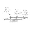
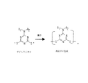
このような酸化処理工程により処理された固体に、トリアジンジチオール誘導体の1種または2種以上の原料を真空蒸着法によって蒸着させると、図1及び図2に示すように、真空中でトリアジンジチオール誘導体の分子を加熱蒸発、昇華し「飛ばす」ことによって、空間のガス分子と衝突することなく固体の表面に分子が堆積する。真空中で蒸発源から飛行し堆積する分子は、固体表面での結晶核の発生、固体表面での拡散などにより衝突、反応し薄膜は成長する。固体表面に均一に分散した結晶核の形成が、その後の膜成長状態に影響し、規則的に分子配列しながら膜成長する。 When one or more raw materials of the triazine dithiol derivative are deposited on the solid treated by such an oxidation treatment step by vacuum deposition, as shown in FIGS. 1 and 2, the triazine dithiol derivative is evacuated in vacuum. The molecules are deposited on the surface of the solid without colliding with gas molecules in the space by heating and evaporating and sublimating the molecules. Molecules flying from the evaporation source in vacuum and depositing collide and react due to generation of crystal nuclei on the solid surface and diffusion on the solid surface, and the thin film grows. Formation of crystal nuclei uniformly dispersed on the solid surface affects the subsequent film growth state, and the film grows while regularly arranging molecules.
詳しくは、図1に示すように、n型半導体表面に到達したトリアジンジチオール誘導体は、固体との衝突の際、固体から電子を授受する。電子が過剰となったトリアジンジチオール誘導体は、トリアジン環に存在する水素を固体に供与し、すぐにチオール基はチイルラジカルとなる。トリアジンジチオールの重合反応は2つのチオール基間のラジカル反応であることから、チイルラジカルの形成は、固体表面での蒸着重合反応を促進すると考えられる。
固体表面に形成したトリアジンジチオール誘導体の蒸着重合膜は、さらに結晶成長を促進し、規則的に分子配列しながら膜成長する。成長した膜の重合処理は、分子間同士の化学反応により3次元的な重合反応が起こり易くなり、被膜強度が向上すると考えられる。また規則配列した官能基が表面に形成することによって、機能付与が可能になる。
Specifically, as shown in FIG. 1, the triazine dithiol derivative that has reached the surface of the n-type semiconductor gives and receives electrons from the solid upon collision with the solid. The triazine dithiol derivative with excess electrons donates the hydrogen present in the triazine ring to the solid, and the thiol group immediately becomes a thiyl radical. Since the polymerization reaction of triazine dithiol is a radical reaction between two thiol groups, the formation of thiyl radical is considered to promote the vapor deposition polymerization reaction on the solid surface.
The vapor deposition polymerization film of the triazine dithiol derivative formed on the solid surface further promotes crystal growth and grows with regular molecular alignment. In the polymerization treatment of the grown film, a three-dimensional polymerization reaction is likely to occur due to a chemical reaction between molecules, and the coating strength is considered to be improved. In addition, functional groups can be imparted by forming regularly arranged functional groups on the surface.
また、必要に応じ、上記n型半導体性を示す金属酸化物として、酸化鉄(Fe2 O3 )、酸化アルミニウム(Al2 O3 )、酸化クロム(Cr2 O3 )、酸化マグネシウム(MgO)、酸化亜鉛(ZnO)、酸化カドミウム(CdO)、酸化ニオブ(NbO2 )、酸化チタン(TiO2 )、酸化バナジウム(VO2 )の少なくとも一種で形成した構成とした。固体の表面に酸化物として容易に形成しやすく、酸化処理工程を簡易なものにすることができる。 If necessary, the metal oxide exhibiting n-type semiconductor properties may be iron oxide (Fe 2 O 3 ), aluminum oxide (Al 2 O 3 ), chromium oxide (Cr 2 O 3 ), magnesium oxide (MgO). , Zinc oxide (ZnO), cadmium oxide (CdO), niobium oxide (NbO 2 ), titanium oxide (TiO 2 ), and vanadium oxide (VO 2 ). It can be easily formed as an oxide on the solid surface, and the oxidation treatment process can be simplified.
そしてまた、必要に応じ、上記酸化処理工程において、先に、固体の表面に鉄(Fe)、アルミニウム(Al)、クロム(Cr)、マグネシウム(Mg)、亜鉛(Zn)、カドミウム(Cd)、ニオブ(Nb)、チタン(Ti)、バナジウム(V)の薄膜を形成し、その後、該薄膜に対して酸化処理を行なう構成とした。これによれば、固体が金属以外のものでも固体の表面に酸化物として容易に形成しやすく、酸化処理工程を簡易なものにすることができる。 In addition, if necessary, in the oxidation treatment step, first, iron (Fe), aluminum (Al), chromium (Cr), magnesium (Mg), zinc (Zn), cadmium (Cd), A thin film of niobium (Nb), titanium (Ti), and vanadium (V) was formed, and then the oxidation treatment was performed on the thin film. According to this, even if the solid is other than metal, it can be easily formed as an oxide on the surface of the solid, and the oxidation treatment process can be simplified.
更に、必要に応じ、上記酸化処理工程において、先に、上記固体の表面にニッケル(Ni)膜を形成し、次に、その上に鉄(Fe)、アルミニウム(Al)、クロム(Cr)、マグネシウム(Mg)、亜鉛(Zn)、カドミウム(Cd)、ニオブ(Nb)、チタン(Ti)、バナジウム(V)の少なくとも一種の薄膜を形成し、その後、該薄膜に対して酸化処理を行なう構成としている。 Further, if necessary, in the oxidation treatment step, first, a nickel (Ni) film is formed on the surface of the solid, and then iron (Fe), aluminum (Al), chromium (Cr), A structure in which at least one thin film of magnesium (Mg), zinc (Zn), cadmium (Cd), niobium (Nb), titanium (Ti), and vanadium (V) is formed, and then the thin film is oxidized. It is said.
これによれば、先に、固体の表面にニッケル(Ni)膜を形成するので、ニッケル(Ni)として機能し、そのため、上記の酸化処理させられる金属を、確実に固体表面に被覆することができる。
ニッケルに酸化処理させられる金属が付着し易くなるのは、以下の理由による。
ニッケルはその酸化膜が非常に薄く、被膜する金属と容易に金属間接合するので、多くの固体表面に強固な金属積層被膜形成ができる。ニッケル以外での金属界面においては、厚い酸化膜によって材料間接合が得られないことから、強固な積層被膜が形成し難い。また、ニッケルは、多くの固体表面に容易に被膜形成できることから、被膜形成の下地処理として有用である。
According to this, since the nickel (Ni) film is first formed on the surface of the solid, it functions as nickel (Ni), so that the metal to be oxidized can be reliably coated on the solid surface. it can.
The reason why the metal to be oxidized is easily attached to nickel is as follows.
Nickel has a very thin oxide film and can easily be metal-to-metal bonded to the metal to be coated, so that a strong metal multilayer coating can be formed on many solid surfaces. At the metal interface other than nickel, it is difficult to form a strong multilayer coating because a thick oxide film cannot provide material-to-material bonding. Moreover, since nickel can easily form a film on many solid surfaces, it is useful as a base treatment for film formation.
本発明のトリアジンジチオール誘導体の高分子薄膜生成方法によれば、トリアジンジチオール誘導体の1種または2種以上のそれぞれからなる各層の薄膜を、固体の表面に真空蒸着法によって混合あるいは積層する際、蒸着の前に、固体の表面にn型半導体性を示す金属酸化物を形成する酸化処理工程を設けたので、固体からの電子の授受により、チオール基がチイルラジカルとなり、そのため、トリアジンジチオールの固体表面での蒸着重合反応が促進され、分子間での高効率な重合反応を行なうことができるようになる。その結果、薄膜の強度を増して耐久性の向上を図ることができる。 According to the method for producing a polymer thin film of a triazine dithiol derivative according to the present invention, when a thin film of each layer composed of one or more of triazine dithiol derivatives is mixed or laminated on a solid surface by a vacuum evaporation method, vapor deposition is performed. Since an oxidation treatment step for forming a metal oxide exhibiting n-type semiconductivity is provided on the surface of the solid, the thiol group becomes a thiyl radical due to the transfer of electrons from the solid. The vapor deposition polymerization reaction is promoted, and a highly efficient polymerization reaction between molecules can be performed. As a result, the strength of the thin film can be increased to improve the durability.
以下、添付図面に基づいて、本発明の実施の形態に係るトリアジンジチオール誘導体の高分子薄膜生成方法について詳細に説明する。
本発明の実施の形態に係るトリアジンジチオール誘導体の高分子薄膜生成方法は、固体表面に一般式
Hereinafter, a method for producing a polymer thin film of a triazinedithiol derivative according to an embodiment of the present invention will be described in detail with reference to the accompanying drawings.
The method for producing a polymer thin film of a triazine dithiol derivative according to an embodiment of the present invention has a general formula on a solid surface.
〔式中、R1 は、H−, CH3 −, C2 H5 −, C4 H9 −, C6 H13−, C8 H17−, C10H21−, C12H25−, C18H37−, C20H41−, C22H45−, C24H49−, CH2 =CHCH2 −, CH2 =CH−(CH2 )8 −, CH2 =CH−(CH2 )9 −, C8 H17CH=CHC8 H16−, C6 H11−, C6 H5 −, C6 H5 CH2 −, C6 H5 CH2 CH2 −, CH2 =CH(CH2 )4 COOCH2 CH2 −, CH2 =CH(CH2 )8 COOCH2 CH2 −, CH2 =CH(CH2 )9 COOCH2 CH2 −, CF3 C6 H4 −, C4 F9 C6 H4 −, C6 F13C6 H4 −, C8 F17C6 H4 −, C10F21C6 H4 −, C6 F11OC6 H4 −, C9 F17OC6 H4 −, C4 F9 CH2 −, C6 F13CH2 −, C8 F17CH2 −, C10F21CH2 −, C4 FCH2 CH2 −, C6 F13CH2 CH2 −, C8 F17CH2 CH2 −, C10F21CH2 CH2 −, C4 F9 CH=CHCH2 −, C6 F13CH2 =CHCH2 −, C8 F17CH=CHCH2 −, C10F21CH=CHCH2 −, C4 F9 CH2 CH(OH)CH2 −, C6 F13CH2 CH(OH)CH2 −, C8 F17CH2 CH(OH)CH2 −, C10F21CH2 CH(OH)CH2 −を意味し、R2 はH−, CH3 −, C2 H5 −, C4 H9 −, C6 H13−, C8 H17−, C10H21−, C12H25−, C18H37−, C20H41−, C22H45−, C24H49−, CH2 =CHCH2 −, CH2 =CH(CH2 )8 −, CH2 =CH(CH2 )9 −, C8 H17CH=CHC8 H16−, C6 H11−, C6 H5 −, C6 H5 CH2 −, C6 H5 CH2 CH2 −, CH2 =CH(CH2 )4 COOCH2 CH2 −, CH2 =CH(CH2 )8 COOCH2 CH2 −, CH2 =CH(CH2 )9 COOCH2 CH2 −, CF3 C6 H4 −, C4 F9 C6 H4 −, C6 F13C6 H4 −, C8 F17C6 H4 −, C10F21C6 H4 −, C6 F11OC6 H4 −, C9 F17OC6 H4 −, C4 F9 CH2 −, C6 F13CH2 −, C8 F17CH2 −, C10F21CH2 −, C4 FCH2 CH2 −, C6 F13CH2 CH2 −, C8 F17CH2 CH2 −, C10F21CH2 CH2 −, C4 F9 CH=CHCH2 −, C6 F13CH=CHCH2 −, C8 F17CH=CHCH2 −, C10F21CH=CHCH2 −, C4 F9 CH2 CH(OH)CH2 −, C6 F13CH2 CH(OH)CH2 −, C8 F17CH2 CH(OH)CH2 −, C10F21CH2 CH(OH)CH2 −またR1 −N−R2 が(CH2 =CH−(CH2 )4 COO(CH2 CH2 ))2 N−,
(CH2 =CH−(CH2 )8 COO(CH2 CH2 ))2 N−,
((CH2 =CH−(CH2 )9 COO(CH2 CH2 ))2−, (C4 F9 COO(CH2 CH2 ))2 N−,
(C6 F13COO(CH2 CH2 ))2 N−,(C8 F17COO(CH2 CH2 ))2 N−,
(C10F21COO(CH2 CH2 ))2 N−である。また、通常MはHとLi,Na,K,Ceなどのアルカリである。〕
で示されるトリアジンジチオール誘導体の1種または2種以上の原料を、固体の表面に真空蒸着法によって混合あるいは積層する高分子薄膜生成方法において、
上記蒸着の前に、上記固体の表面にn型半導体性を示す金属酸化物を形成する酸化処理工程を設けた構成としている。
[Wherein R 1 represents H-, CH 3- , C 2 H 5- , C 4 H 9- , C 6 H 13- , C 8 H 17- , C 10 H 21- , C 12 H 25- , C 18 H 37 -, C 20 H 41 -, C 22 H 45 -, C 24 H 49 -, CH 2 = CHCH 2 -, CH 2 = CH- (CH 2) 8 -, CH 2 = CH- ( CH 2) 9 -, C 8 H 17 CH = CHC 8 H 16 -, C 6 H 11 -, C 6 H 5 -, C 6 H 5 CH 2 -, C 6 H 5 CH 2 CH 2 -, CH 2 = CH (CH 2) 4 COOCH 2 CH 2 -, CH 2 = CH (CH 2) 8 COOCH 2 CH 2 -, CH 2 = CH (CH 2) 9 COOCH 2 CH 2 -, CF 3 C 6 H 4 - C 4 F 9 C 6 H 4 −, C 6 F 13 C 6 H 4 −, C 8 F 17 C 6 H 4 −, C 10 F 21 C 6 H 4 −, C 6 F 11 OC 6 H 4 − , C 9 F 17 OC 6 H 4 -, C 4 F 9 CH 2 -, C 6 F 13 CH 2 -, C 8 F 17 CH 2 -, C 10 F 21 CH 2 -, C 4 FCH 2 CH 2 -, C 6 F 13 CH 2 CH 2 -, C 8 F 17 CH 2 CH 2 -, C 10 F 21 CH 2 CH 2 -, C 4 F 9 CH = CHCH 2 -, C 6 F 13 CH 2 = CHCH 2 -, C 8 F 17 CH = CHCH 2 -, C 10 F 21 CH = CHCH 2 - , C 4 F 9 CH 2 CH (OH) CH 2 -, C 6 F 13 CH 2 CH (OH) CH 2 -, C 8 F 17 CH 2 CH (OH) CH 2 -, C 10 F 21 CH 2 CH (OH) CH 2- means R 2 is H-, CH 3- , C 2 H 5- , C 4 H 9- , C 6 H 13- , C 8 H 17- , C 10 H 21- , C 12 H 25 -, C 18 H 37 -, C 20 H 41 -, C 22 H 45 -, C 24 H 49 -, CH 2 = CHCH 2 -, CH 2 = CH (CH 2) 8 -, CH 2 = CH (CH 2) 9 - , C 8 H 17 CH═CHC 8 H 16 −, C 6 H 11 −, C 6 H 5 −, C 6 H 5 CH 2 −, C 6 H 5 CH 2 CH 2 −, CH 2 ═CH (CH 2 ) 4 COOCH 2 CH 2 -, CH 2 = CH (CH 2) 8 COOCH 2 CH 2 -, CH 2 = CH (CH 2) 9 COOCH 2 CH 2 -, CF 3 C 6 H 4 -, C 4 F 9 C 6 H 4 −, C 6 F 13 C 6 H 4 −, C 8 F 17 C 6 H 4 −, C 10 F 21 C 6 H 4 −, C 6 F 11 OC 6 H 4 −, C 9 F 17 OC 6 H 4 -, C 4 F 9 CH 2 -, C 6 F 13 CH 2 -, C 8 F 17 CH 2 -, C 10 F 21 CH 2 -, C 4 FCH 2 CH 2 -, C 6 F 13 CH 2 CH 2- , C 8 F 17 CH 2 CH 2- , C 10 F 21 CH 2 CH 2- , C 4 F 9 CH = CHCH 2- , C 6 F 13 CH = CHCH 2- , C 8 F 17 CH = CHCH 2 −, C 10 F 2 1 CH = CHCH 2 -, C 4 F 9 CH 2 CH (OH) CH 2 -, C 6 F 13 CH 2 CH (OH) CH 2 -, C 8 F 17 CH 2 CH (OH) CH 2 -, C 10 F 21 CH 2 CH (OH) CH 2 — or R 1 —N—R 2 is (CH 2 ═CH— (CH 2 ) 4 COO (CH 2 CH 2 )) 2 N—,
(CH 2 = CH- (CH 2 ) 8 COO (CH 2 CH 2)) 2 N-,
((CH 2 = CH- (CH 2) 9 COO (CH 2 CH 2)) 2 -, 2 N- (C 4
(C 6 F 13 COO (CH 2 CH 2)) 2 N -, 2 N- (C 8
(C 10 F 21 COO (CH 2 CH 2)) 2 is N-. Usually, M is an alkali such as H and Li, Na, K, and Ce. ]
In a method for producing a polymer thin film in which one or more raw materials of a triazine dithiol derivative represented by the formula (1) are mixed or laminated on a solid surface by a vacuum deposition method,
Prior to the vapor deposition, an oxidation treatment process for forming a metal oxide exhibiting n-type semiconductivity on the surface of the solid is provided.
機能性トリアジンジチオール誘導体は、目的に応じて合成することができる。真空蒸着法により、これらの有機化合物はn型半導体性を示す表面に被膜形成する。真空めっき法によって生成したトリアジンジチオール誘導体被膜は、モノマーあるいは低分子状態である。この被膜を重合することによって耐久性のある実用的な高分子膜となり得る。
ここで用いるn型半導体表面とは、トリアジンジチオール誘導体に電子を供給する作用を示すものである。たとえば、金属酸化物は還元性雰囲気では、酸素を失って、陽イオンと電子を生ずる。この電子がn型半導体として作用する。または、蒸着金属膜では、真空中の微量の酸素により酸化し、そのまま真空中に放置したTiやCrでは金属過剰な酸化物としてn型半導体性を示す。あるいは、Alや、Fe、Mg、Zn、Cd、Nb、Vなどの蒸着膜を大気放置した酸化膜はn型半導体性を示す。
A functional triazine dithiol derivative can be synthesized according to the purpose. These organic compounds form a film on the surface exhibiting n-type semiconductivity by a vacuum deposition method. The triazine dithiol derivative coating produced by the vacuum plating method is in a monomer or low molecular state. By polymerizing this film, a durable and practical polymer film can be obtained.
The n-type semiconductor surface used here indicates the function of supplying electrons to the triazine dithiol derivative. For example, metal oxides lose oxygen and produce cations and electrons in a reducing atmosphere. This electron acts as an n-type semiconductor. Alternatively, a deposited metal film is oxidized by a small amount of oxygen in a vacuum, and Ti or Cr left in the vacuum as it is exhibits an n-type semiconductor property as a metal-excess oxide. Alternatively, an oxide film in which a deposited film such as Al, Fe, Mg, Zn, Cd, Nb, and V is left in the air exhibits n-type semiconductor properties.
酸化処理工程としては、以下の態様のものがある。固体そのものが酸化によりn型半導体性を示す金属である場合は、空気などの酸化させることができる気体により酸化処理を行ない、あるいは酸化させることができる液体により酸化処理を行なう等する。
また、固体そのものが酸化によりn型半導体性を示さない金属であったり、金属以外の物質で構成されているものにあっては、固体表面に直接n型半導体性を示す酸化金属を付着させ、あるいは酸化によりn型半導体性を示す金属を付着させ、その後、空気などの酸化させることができる気体により酸化処理を行ない、あるいは酸化させることができる液体により酸化処理を行なう等する。
The oxidation treatment process includes the following aspects. When the solid itself is a metal that exhibits n-type semiconductivity by oxidation, the oxidation treatment is performed with a gas that can be oxidized, such as air, or the oxidation treatment is performed with a liquid that can be oxidized.
In addition, in the case where the solid itself is a metal that does not exhibit n-type semiconductivity by oxidation or is composed of a substance other than a metal, a metal oxide that exhibits n-type semiconductivity is directly attached to the solid surface, Alternatively, a metal exhibiting n-type semiconductivity is attached by oxidation, and thereafter, oxidation treatment is performed with a gas that can be oxidized, such as air, or oxidation treatment is performed with a liquid that can be oxidized.
固体とは、鉄、鋳鉄、およびステンレス、パーマロイ、銅、黄銅、リン青銅、ニッケル、キュブロニッケル、錫、鉛、コバルト、半田、チタン、アルミニウム、クロム、金、銀、白金、パラジウム、亜鉛などの金属をはじめ、これらの酸化物、リン酸塩処理金属、クロム酸塩処理金属、シリコン、カーボン、化合物半導体、酸化アルミナセラミックス、陶器、ガラス、石英ガラス、超電導体セラミックス、木材、紙、プラスチックス、エンジニアリングプラスチックス、熱硬化性樹脂などどのようなものでもよい。 Solids include iron, cast iron, stainless steel, permalloy, copper, brass, phosphor bronze, nickel, cubro nickel, tin, lead, cobalt, solder, titanium, aluminum, chromium, gold, silver, platinum, palladium, zinc, etc. In addition to these metals, these oxides, phosphate-treated metals, chromate-treated metals, silicon, carbon, compound semiconductors, alumina oxide ceramics, ceramics, glass, quartz glass, superconductor ceramics, wood, paper, plastics , Engineering plastics, thermosetting resins, etc.
これらの表面にn型半導体性を示す金属酸化物(例えば、酸化鉄(Fe2 O3 )、酸化クロム(Cr2 O3 )、酸化マグネシウム(MgO)、酸化亜鉛(ZnO)、酸化カルシウム(CaO)、酸化チタン(TiO2 )、酸化バナジウム(VO2 )、リン(P)あるいはアンチモン(Sb)等をドープしたシリコンなど)をスパッター法や、真空蒸着法で薄膜形成する。あるいは、例えば鉄(Fe)やマグネシウム(Mg)、あるいはアルミニウム(Al)などの金属薄膜を作製し、これを大気放置することによって、n型半導体性を示す金属酸化物を形成できる。あるいは、鋼板や、亜鉛板、亜鉛めっき、クロム板、クロムめっき表面などに酸化膜を形成することも可能である。 Metal oxides (for example, iron oxide (Fe 2 O 3 ), chromium oxide (Cr 2 O 3 ), magnesium oxide (MgO), zinc oxide (ZnO), calcium oxide (CaO) exhibiting n-type semiconductivity on their surfaces. ), Titanium oxide (TiO 2 ), vanadium oxide (VO 2 ), phosphorus (P), silicon doped with antimony (Sb), or the like) is formed into a thin film by sputtering or vacuum deposition. Alternatively, for example, a metal thin film such as iron (Fe), magnesium (Mg), or aluminum (Al) is produced and left in the atmosphere, whereby a metal oxide exhibiting n-type semiconductor properties can be formed. Alternatively, an oxide film can be formed on a steel plate, a zinc plate, a zinc plate, a chromium plate, a chromium plating surface, or the like.
また、還元処理によっても、n型半導体の特性を示す固体表面が得られる。還元処理として、鋼板や、亜鉛板、亜鉛めっき、クロム板、クロムめっき、チタン板などを還元雰囲気で表面処理する場合では、化学的には、例えばヒドラジン化合物、水素化ホウ素ナトリウム、あるいは次亜りん酸ナトリウムなどの還元剤にて浸漬処理する方法がある。還元剤の水溶液に固体を入れる。水溶液濃度は薄いと還元能力が発揮されず、濃いと固体表面を改質するため、好ましくは0.1〜20wt%の濃度で使う。処理温度は80℃以下である。低すぎると固体表面の還元反応が進まないため、室温以上がよい。浸漬時間は濃度や温度により左右され、その範囲は固定されない。固体表面の外観が変化しないよう確認しながら行なう。処理後は、処理液の残渣を除く目的で、アルコールを用いすすぎ洗浄し、乾燥する。アルコール洗浄は乾きムラを抑えるのに有効である。また、物理的方法として、例えば真空装置に酸素ガスを導入し、高周波プラズマ状態にすると、酸素はイオン化される。固体表面を陽極に電位を印加すると酸素イオンが注入され、電子が過剰なn型半導体の特性を示す固体表面が得られる。 Moreover, the solid surface which shows the characteristic of an n-type semiconductor is also obtained by reduction treatment. As a reduction treatment, when a steel plate, zinc plate, zinc plating, chromium plate, chromium plating, titanium plate, or the like is surface-treated in a reducing atmosphere, chemically, for example, a hydrazine compound, sodium borohydride, or hypophosphorous acid. There is a method of immersion treatment with a reducing agent such as sodium acid. A solid is placed in an aqueous solution of a reducing agent. When the concentration of the aqueous solution is low, the reducing ability is not exhibited. When the concentration is high, the solid surface is modified. Therefore, the concentration is preferably 0.1 to 20 wt%. The processing temperature is 80 ° C. or lower. If it is too low, the reduction reaction on the surface of the solid does not proceed. The immersion time depends on the concentration and temperature, and the range is not fixed. Confirming that the appearance of the solid surface does not change. After the treatment, for the purpose of removing the residue of the treatment liquid, it is rinsed with alcohol and dried. Alcohol cleaning is effective in suppressing drying unevenness. Further, as a physical method, for example, oxygen is ionized when oxygen gas is introduced into a vacuum apparatus to form a high-frequency plasma state. When a potential is applied to the anode of the solid surface, oxygen ions are implanted to obtain a solid surface exhibiting the characteristics of an n-type semiconductor with excess electrons.
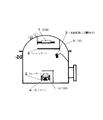
次に、真空蒸着装置について説明する。真空蒸着装置は、例えば、図3に示されるように、モノマー4であるトリアジンジチオール誘導体の入ったるつぼ1と、トリアジンジチオール誘導体を蒸発させるヒーター2と、蒸着する固体7および蒸着した被膜の厚さを計る水晶振動子式膜厚計3とを備えてなり、これらが収納された室5に真空ポンプ(図示省略)が連結されている。6は蒸発源と固体7との間にあるメインシャッターである。
Next, a vacuum deposition apparatus will be described. For example, as shown in FIG. 3, the vacuum vapor deposition apparatus includes a
したがって、この真空蒸着装置によりトリアジンジチオール誘導体を加熱蒸発させ、これをある固体表面に付着させるときは以下のようになる。固体7の表面の温度は50℃以下である。50℃以上では、光照射による重合が起こり難く、また、あまり冷却しすぎても、付着面を取出すときに結露等の不具合があり、実用的ではない。好ましくは0℃〜50℃である。また、真空度は一般に1.0〜1.0×10⁻⁶〔Pa〕、望ましくは、1.0×10⁻¹〜1.0×10⁻⁴〔Pa〕である。ヒーター2の温度は室温から250℃、望ましくは、50〜200℃であるが、トリアジンジチオールの分子量および真空度とヒーター温度との兼ね合いで最適な蒸着条件が決まり、一義的に定めることはできない。 Therefore, when the triazine dithiol derivative is heated and evaporated by this vacuum deposition apparatus and is attached to a solid surface, the following occurs. The temperature of the surface of the solid 7 is 50 ° C. or less. Above 50 ° C., polymerization due to light irradiation hardly occurs, and even if it is cooled too much, there are problems such as condensation when taking out the adhered surface, which is not practical. Preferably it is 0 degreeC-50 degreeC. The degree of vacuum is generally 1.0 to 1.0 × 10 −6 [Pa], and preferably 1.0 × 10 −1 to 1.0 × 10 −4 [Pa]. The temperature of the heater 2 is from room temperature to 250 ° C., preferably 50 to 200 ° C., but the optimum deposition conditions are determined by the balance between the molecular weight of triazinedithiol and the degree of vacuum and the heater temperature, and cannot be uniquely determined.
そして、電離真空計を用いて装置内を一定の真空度に調整後、蒸発源のるつぼ1あるいはヒーター2をそれぞれ加熱して1種あるいは2種のトリアジンジチオール誘導体を気化、あるいは昇華させる。このとき、蒸発源と固体7との間にあるメインシャッター6は閉じておく。トリアジンジチオール誘導体が気化、あるいは昇華していることを水晶振動子式膜厚計3により確認したならば、蒸発速度を予定の値に調整し、整ったところでシャッター6を開き、蒸着を開始する。
目的の膜厚になったならば、メインシャッター6を閉じて、蒸発源の加熱をやめる。そして、るつぼ1およびヒーター2が充分に冷えたところで、大気ベントを行ない、固体7を取出す。
Then, after adjusting the inside of the apparatus to a certain degree of vacuum using an ionization vacuum gauge, the
When the target film thickness is reached, the main shutter 6 is closed and heating of the evaporation source is stopped. When the
この真空蒸着装置による蒸着においては、図1及び図2に示すように、真空中でトリアジンジチオール誘導体の分子を加熱蒸発、昇華し「飛ばす」ことによって、空間のガス分子と衝突することなく固体表面に堆積させる。これは、多くの固体表面に分子を堆積させて薄膜を作製することができる手法である。真空中で蒸発源から飛行し堆積する分子は、固体表面での結晶核の発生、固体表面での拡散などにより衝突、反応し薄膜は成長する。固体表面に均一に分散した結晶核の形成が、その後の膜成長状態に影響し、規則的に分子配列しながら膜成長する。n型半導体表面に到達したトリアジンジチオール誘導体は、固体との衝突の際、固体から電子を授受する。電子が過剰となったトリアジンジチオールは、トリアジン環に存在する水素を固体に供与し、すぐにチオール基はチイルラジカルとなる。トリアジンジチオールの重合反応は2つのチオール基間のラジカル反応であることから、チイルラジカルの形成は、固体表面での蒸着重合反応を促進すると考えられる。
固体表面に形成したトリアジンジチオール誘導体の蒸着重合膜は、さらに結晶成長を促進し、規則的に分子配列しながら膜成長する。成長した膜の重合処理は、分子間同士の化学反応により3次元的な重合反応が起こり易くなり、被膜強度が向上すると考えられる。また規則配列した官能基が表面に形成することによって、機能付与が可能になる。
In the vapor deposition by this vacuum vapor deposition apparatus, as shown in FIG. 1 and FIG. 2, the solid surface is obtained without colliding with gas molecules in the space by heating and evaporating and subliming the molecules of the triazine dithiol derivative in vacuum. To deposit. This is a technique capable of producing a thin film by depositing molecules on many solid surfaces. Molecules flying from the evaporation source in vacuum and depositing collide and react due to generation of crystal nuclei on the solid surface and diffusion on the solid surface, and the thin film grows. Formation of crystal nuclei uniformly dispersed on the solid surface affects the subsequent film growth state, and the film grows while regularly arranging molecules. The triazine dithiol derivative that has reached the surface of the n-type semiconductor gives and receives electrons from the solid when colliding with the solid. The triazine dithiol with excess electrons donates the hydrogen present in the triazine ring to the solid, and immediately the thiol group becomes a thiyl radical. Since the polymerization reaction of triazine dithiol is a radical reaction between two thiol groups, the formation of thiyl radical is considered to promote the vapor deposition polymerization reaction on the solid surface.
The vapor deposition polymerization film of the triazine dithiol derivative formed on the solid surface further promotes crystal growth and grows with regular molecular alignment. In the polymerization treatment of the grown film, a three-dimensional polymerization reaction is likely to occur due to a chemical reaction between molecules, and the coating strength is considered to be improved. In addition, functional groups can be imparted by forming regularly arranged functional groups on the surface.
本実施の形態においては、その後、光重合による後処理を行なっている。これは、得られた被膜に、市販の波長切り替え型ハンディUVランプ(アズワン(株)製:SLUV−8)を用い(波長:245nm〜400nm:出力約9W)、照射距離を60mmとし、室温(約23℃)にて紫外線を照射し重合被膜を得た。
光重合に用いる照射条件は、照射雰囲気が大きく左右する。波長は大気中で光照射する場合は、280〜400nmが好ましく、真空中では245nm〜400nmの波長が好ましい。
大気中での照射の場合、280nmに満たない波長は、酸素や水分がラジカルを生成し、酸化劣化を引き起こしやすいことに起因する。また、単波長は微量の酸素等によって散乱、吸収されることから、照射距離は20cm以下が好ましく、反応速度も速いことから短時間の照射が好ましく、適宜、選定される。
In this embodiment, after-treatment by photopolymerization is then performed. This uses a commercially available wavelength-switchable handy UV lamp (manufactured by AS ONE: SLUV-8) for the obtained coating (wavelength: 245 nm to 400 nm: output about 9 W), an irradiation distance of 60 mm, and room temperature ( (About 23 ° C.) was irradiated with ultraviolet rays to obtain a polymer film.
Irradiation atmosphere greatly affects the irradiation conditions used for photopolymerization. The wavelength is preferably 280 to 400 nm when irradiated with light in the air, and preferably 245 to 400 nm in vacuum.
In the case of irradiation in the atmosphere, the wavelength of less than 280 nm is due to the fact that oxygen and moisture generate radicals and are likely to cause oxidative degradation. In addition, since the single wavelength is scattered and absorbed by a small amount of oxygen or the like, the irradiation distance is preferably 20 cm or less, and since the reaction rate is fast, irradiation for a short time is preferable and is selected as appropriate.
以下、本発明の実施例を、比較例とともに示す。
〔実施例1〜10、付着面近傍への被膜生成と光重合〕
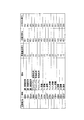
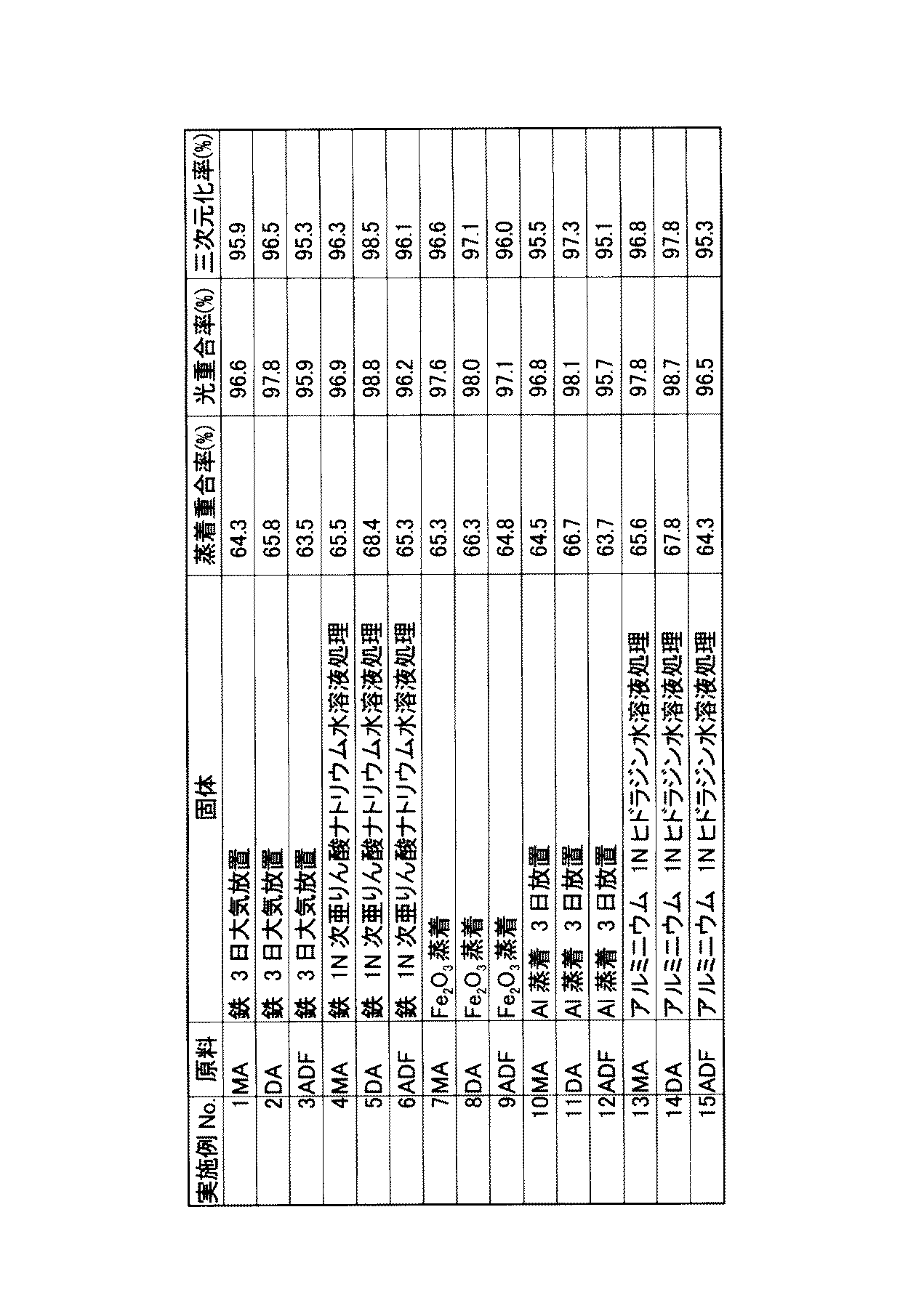
図3に示される真空蒸着装置を用い、図4に示すように、6−アリルアミノ−1,3,5−トリアジン−2、4−ジチオール(図では「MA」と表記)(図4、No.1)、6−ジアリルアミノ−1,3,5−トリアジン−2,4−ジチオール(図では「DA」と表記)(図4、No.2)、及びアリルデシルパーフルオロエチルアミノ−1,3,5−トリアジン−2,4−ジチオール(図では「ADF」と表記)(図4、No.3)をるつぼ1に入れ、固体として鉄板(0.2×3×5cm、アセトンで脱脂)を取付ける。
Examples of the present invention will be described below together with comparative examples.
[Examples 1 to 10, film formation and photopolymerization near the adhesion surface]
As shown in FIG. 4, 6-allylamino-1,3,5-triazine-2,4-dithiol (denoted as “MA” in the figure) (see FIG. 1), 6-diallylamino-1,3,5-triazine-2,4-dithiol (denoted as “DA” in the figure) (FIG. 4, No. 2), and allyldecylperfluoroethylamino-1,3 , 5-triazine-2,4-dithiol (denoted as “ADF” in the figure) (FIG. 4, No. 3) is put in the
この鉄板は脱脂洗浄後大気に3日間放置して酸化処理させた固体である。真空ポンプを作動させ、電離真空計により真空度が5×10⁻³Paに達したら、第1蒸発源ヒーター2の温度を110℃〜160℃まであげて、成膜速度が約0.02nm/secであることを確認する。所定の成膜速度になったらメインシャッター6を開け、水晶振動子式膜厚計3にて計測して厚さ3nmと50nmの被膜を得た。所定の膜厚になったら、メインシャッター6を閉じる。ヒーター2を切り、充分に冷えたところで、大気ベントを行ない、固体7を取出す。
This iron plate is a solid that has been oxidized and left in the atmosphere for 3 days after degreasing and cleaning. When the vacuum pump is activated and the degree of vacuum reaches 5 × 10 −3 Pa by an ionization vacuum gauge, the temperature of the first evaporation source heater 2 is increased to 110 ° C. to 160 ° C., and the film formation rate is about 0.02 nm / Confirm that it is sec. When the predetermined film formation speed was reached, the main shutter 6 was opened, and the film was measured with a crystal oscillator type
得られた厚さ3nm被膜の蒸着重合率を測定した。トリアジンジチオール化合物のモノマーはアルコールに可溶なことから、固体近傍での蒸着重合率はアルコールに20℃で24時間浸漬、乾燥後、膜厚をエリプソメータにより測定して残存率から算出した。 The vapor deposition polymerization rate of the obtained 3 nm-thick film was measured. Since the monomer of the triazine dithiol compound is soluble in alcohol, the vapor deposition polymerization rate in the vicinity of the solid was calculated from the remaining rate by measuring the film thickness with an ellipsometer after being immersed in alcohol at 20 ° C. for 24 hours and drying.
得られた50nmの被膜に、市販の波長切り替え型ハンディUVランプ(アズワン(株)製:SLUV−8)を用い(波長:280nm〜400nm:出力約9W)、照射距離を60mmとし、室温(約23℃)にて60分間照射し重合被膜を得た。被膜の重合率(アルコール不溶率)と、三次元化率(テトラヒドロフラン(THF)に対する不溶率)を測定した。重合率はアルコールに20℃で24時間浸漬、乾燥後、また三次元化率はTHFに20℃で24時間浸漬、乾燥後、膜厚をエリプソメータにより測定して求めた。 A commercially available wavelength-switchable handy UV lamp (manufactured by ASONE: SLUV-8) was used for the obtained 50 nm film (wavelength: 280 nm to 400 nm: output about 9 W), the irradiation distance was set to 60 mm, and room temperature (about (23 ° C.) for 60 minutes to obtain a polymerized film. The polymerization rate (alcohol insolubility rate) and the three-dimensionalization rate (insolubility rate with respect to tetrahydrofuran (THF)) of the film were measured. The polymerization rate was determined by immersing in alcohol at 20 ° C. for 24 hours and drying, and the three-dimensional ratio was determined by immersing and drying in THF at 20 ° C. for 24 hours and then measuring the film thickness with an ellipsometer.
また、実施例においては、固体である脱脂洗浄の鉄板を1Nの次亜りん酸ナトリウム水溶液に30分浸漬処理して酸化処理を行ない、その後メタノールにてすすぎ洗浄した固体を用いた。図4に示すように、6−アリルアミノ−1,3,5−トリアジン−2,4−ジチオール(図4、No.4)、6−ジアリルアミノ−1,3,5−トリアジン−2,4−ジチオール(図4、No.5)、及びアリルデシルパーフルオロエチルアミノ−1,3,5−トリアジン−2,4−ジチオール(図4、No.6)の薄膜を作製し、蒸着重合率、光重合率および三次元化率を求めた。 Further, in the examples, a solid that was degreased and washed and was solid-treated by immersing it in a 1N sodium hypophosphite aqueous solution for 30 minutes, followed by rinsing with methanol was used. As shown in FIG. 4, 6-allylamino-1,3,5-triazine-2,4-dithiol (FIG. 4, No. 4), 6-diallylamino-1,3,5-triazine-2,4- Thin films of dithiol (FIG. 4, No. 5) and allyl decyl perfluoroethylamino-1,3,5-triazine-2,4-dithiol (FIG. 4, No. 6) were prepared, vapor deposition polymerization rate, light The polymerization rate and the three-dimensionalization rate were determined.
更に、実施例として、図4に示すように、鉄製の固体に20nmのニッケル(Ni)を蒸着し、Fe2 O3 原料を100nm蒸着したものを用いた。得られたFe2 O3 の固体表面に6−アリルアミノ−1,3,5−トリアジン−2,4−ジチオール(図4、No.7)、6−ジアリルアミノ−1,3,5−トリアジン−2,4−ジチオール(図4、No.8)、及びアリルデシルパーフルオロエチルアミノ−1,3,5−トリアジン−2,4−ジチオール(図4、No.9)の薄膜を作製し、蒸着重合率、光重合率および三次元化率を求めた。 Furthermore, as an example, as shown in FIG. 4, 20 nm nickel (Ni) was vapor-deposited on an iron solid and Fe 2 O 3 raw material was vapor deposited to 100 nm. On the solid surface of the obtained Fe 2 O 3 , 6-allylamino-1,3,5-triazine-2,4-dithiol (FIG. 4, No. 7), 6-diallylamino-1,3,5-triazine- Thin films of 2,4-dithiol (FIG. 4, No. 8) and allyldecylperfluoroethylamino-1,3,5-triazine-2,4-dithiol (FIG. 4, No. 9) were prepared and evaporated. The polymerization rate, photopolymerization rate and three-dimensionalization rate were determined.
更にまた、図4に示すように、実施例として、鉄製の固体に20nmのニッケル(Ni)を蒸着し、その後直ちにAlを100nm蒸着し、得られたAl表面を23℃で65%湿度の大気雰囲気に3日間放置して酸化処理を行なった固体も用いた。この固体に6−アリルアミノ−1,3,5−トリアジン−2,4−ジチオール(図4、No.10)、6−ジアリルアミノ−1,3,5−トリアジン−2,4−ジチオール(図4、No.11)、及びアリルデシルパーフルオロエチルアミノ−1,3,5−トリアジン−2,4−ジチオール(図4、No.12)の薄膜を作製し、蒸着重合率、光重合率および三次元化率を求めた。 Furthermore, as shown in FIG. 4, as an example, 20 nm of nickel (Ni) was vapor-deposited on an iron solid, and then Al was vapor-deposited 100 nm. The resulting Al surface was air at 23 ° C. and 65% humidity. A solid which was left in the atmosphere for 3 days and then oxidized was also used. To this solid, 6-allylamino-1,3,5-triazine-2,4-dithiol (FIG. 4, No. 10), 6-diallylamino-1,3,5-triazine-2,4-dithiol (FIG. 4). , No. 11), and allyl decyl perfluoroethylamino-1,3,5-triazine-2,4-dithiol (FIG. 4, No. 12) thin films were prepared, vapor deposition polymerization rate, photopolymerization rate and tertiary The normalization rate was obtained.
また、実施例として、図4に示すように、Alの固体を1Nのヒドラジン水溶液に5分浸漬処理して酸化処理し、その後メタノールにてすすぎ洗浄した固体を用いた。図4に示すように、この固体に、6−アリルアミノ−1,3,5−トリアジン−2,4−ジチオール(図4、No.13)、6−ジアリルアミノ−1,3,5−トリアジン−2,4−ジチオール(図4、No.14)、及びアリルデシルパーフルオロエチルアミノ−1,3,5−トリアジン−2,4−ジチオール(図4、No.15)の薄膜を作製し、蒸着重合率、光重合率および三次元化率を求めた。 In addition, as an example, as shown in FIG. 4, a solid obtained by immersing Al solid in a 1N hydrazine aqueous solution for 5 minutes, oxidizing, and then rinsing with methanol was used. As shown in FIG. 4, 6-allylamino-1,3,5-triazine-2,4-dithiol (FIG. 4, No. 13), 6-diallylamino-1,3,5-triazine- Thin films of 2,4-dithiol (FIG. 4, No. 14) and allyldecylperfluoroethylamino-1,3,5-triazine-2,4-dithiol (FIG. 4, No. 15) were prepared and evaporated. The polymerization rate, photopolymerization rate and three-dimensionalization rate were determined.
次に、比較例を示す。図5には、比較例16〜21を示す。実施例1〜3および13〜15と同様の材質の固体を用い、真空蒸着法による被膜生成時に、脱脂洗浄のみした酸化処理を施さない固体を準備した。 Next, a comparative example is shown. FIG. 5 shows Comparative Examples 16-21. A solid of the same material as in Examples 1 to 3 and 13 to 15 was used, and a solid that was only subjected to degreasing and was not subjected to oxidation treatment was prepared when a film was formed by a vacuum deposition method.
詳しくは、比較例として、鉄製の固体に電解鉄を100nm蒸着したものを用いた。この固体に、その後、真空中でそのまま6−アリルアミノ−1,3,5−トリアジン−2,4−ジチオール(図5、No.22)、6−ジアリルアミノ−1,3,5−トリアジン−2,4−ジチオール(図5、No.23)、及びアリルデシルパーフルオロエチルアミノ−1,3,5−トリアジン−2,4−ジチオール(図5、No.24)の薄膜を作製し、蒸着重合率、光重合率および三次元化率を求めた。 Specifically, as a comparative example, an iron solid deposited with 100 nm of electrolytic iron was used. Thereafter, 6-allylamino-1,3,5-triazine-2,4-dithiol (FIG. 5, No. 22), 6-diallylamino-1,3,5-triazine-2 was directly added to this solid in a vacuum. , 4-dithiol (FIG. 5, No. 23) and allyl decyl perfluoroethylamino-1,3,5-triazine-2,4-dithiol (FIG. 5, No. 24) thin films were prepared, and vapor deposition polymerization was performed. The rate, photopolymerization rate and three-dimensionalization rate were determined.
比較例25〜27は、鉄製の固体に20nmのニッケル(Ni)を蒸着し、その後直ちにFe3 O4 原料を蒸着したものを用いた。得られたFe3 O4 固体表面に6−アリルアミノ−1,3,5−トリアジン−2,4−ジチオール(図5、No.25)、6−ジアリルアミノ−1,3,5−トリアジン−2,4−ジチオール(図5、No.26)、及びアリルデシルパーフルオロエチルアミノ−1,3,5−トリアジン−2,4−ジチオール(図5、No.27)の薄膜を作製し、蒸着重合率、光重合率および三次元化率を求めた。 In Comparative Examples 25 to 27, 20 nm of nickel (Ni) was vapor-deposited on an iron solid, and then an Fe 3 O 4 raw material was immediately vapor deposited. On the obtained Fe 3 O 4 solid surface, 6-allylamino-1,3,5-triazine-2,4-dithiol (FIG. 5, No. 25), 6-diallylamino-1,3,5-triazine-2 , 4-dithiol (FIG. 5, No. 26), and allyl decyl perfluoroethylamino-1,3,5-triazine-2,4-dithiol (FIG. 5, No. 27) thin films were prepared, and vapor deposition polymerization was performed. The rate, photopolymerization rate and three-dimensionalization rate were determined.
また、比較例として、鉄製の固体に20nmのニッケル(Ni)を蒸着し、その後直ちにAlを100nm蒸着したものを用いた。この固体に、その後、真空中でそのまま6−アリルアミノ−1,3,5−トリアジン−2,4−ジチオール(図5、No.28)、6−ジアリルアミノ−1,3,5−トリアジン−2,4−ジチオール(図5、No.29)、及びアリルデシルパーフルオロエチルアミノ−1,3,5−トリアジン−2,4−ジチオール(図5、No.30)の薄膜を作製し、蒸着重合率、光重合率および三次元化率を求めた。 Further, as a comparative example, 20 nm nickel (Ni) was vapor-deposited on an iron solid, and then Al was vapor-deposited 100 nm immediately thereafter. Thereafter, 6-allylamino-1,3,5-triazine-2,4-dithiol (FIG. 5, No. 28), 6-diallylamino-1,3,5-triazine-2 was directly added to this solid in a vacuum. , 4-dithiol (FIG. 5, No. 29), and allyl decyl perfluoroethylamino-1,3,5-triazine-2,4-dithiol (FIG. 5, No. 30) thin films were prepared, and vapor deposition polymerization was performed. The rate, photopolymerization rate and three-dimensionalization rate were determined.
図4及び図5には、上記の実施例と比較例において、蒸着重合率、光重合率および三次元化率の結果が示され、この結果によれば、図4に示すように、実施例に係る固体表面に形成した被膜の蒸着重合率、光重合率、特に3次元化率が高い傾向にある。一方、図5に示すように、比較例に係る固体表面に形成した被膜の蒸着重合率、光重合率、特に3次元化率が低いことが分かる。 4 and 5 show the results of the vapor deposition polymerization rate, the photopolymerization rate, and the three-dimensionalization rate in the above-described examples and comparative examples. According to this result, as shown in FIG. There is a tendency that the vapor deposition polymerization rate, photopolymerization rate, particularly the three-dimensionalization rate of the coating formed on the solid surface is high. On the other hand, as shown in FIG. 5, it turns out that the vapor deposition polymerization rate of the film formed on the solid surface concerning a comparative example, a photopolymerization rate, especially a three-dimensionalization rate are low.
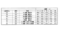
次に、図6に示すように、別の実施例31〜37について示す。この実施例においては、真空めっき法による被膜生成時の付着面として、ガラス固体を用いた。このガラス固体に真空蒸着法により20nmのニッケル(Ni)を蒸着し、その後直ちに鉄(Fe:実施例31)、アルミニウム(Al:実施例32)、マグネシウム(Mg:実施例33)、亜鉛(Zn:実施例34)、バナジウム(V:実施例35)の各材料を用いて100nmの薄膜作製した付着面を用いた。それぞれ大気に3日間放置した固体表面に6−ジアリルアミノ−1,3,5−トリアジン−2,4−ジチオールを用いて50nmの被膜を得た。また、ガラス固体に、真空蒸着法によりクロム(Cr:実施例36)、チタン(Ti:実施例37)の各材料を用いて100nmの薄膜作製した付着面を用い、真空中でそのまま6−ジアリルアミノ−1,3,5−トリアジン−2,4−ジチオールを用いて50nmの被膜を得た。その後、市販の波長切り替え型ハンディUVランプ(アズワン(株)製:SLUV−8)を用い(波長:280nm〜400nm:出力約9W)、照射距離を60mmとし、室温(約23℃)にて150分間照射し重合被膜を得た。蒸着膜の耐久性評価は、スガ式磨耗試験機(スガ試験機(株)NUS−ISO−1)を用いて行なった。摩擦試験接触部に綿製の布(ベンコット:旭化成工業(株)規格 M−3)を貼り付け、試験荷重200gにて20回ごと摩擦試験後の、被膜厚変化をエリプソメータにて計測した。 Next, as shown in FIG. 6, another Example 31-37 is shown. In this example, a glass solid was used as an adhesion surface when a film was formed by vacuum plating. On this glass solid, 20 nm of nickel (Ni) was deposited by vacuum deposition, and immediately thereafter iron (Fe: Example 31), aluminum (Al: Example 32), magnesium (Mg: Example 33), zinc (Zn) : Example 34), Vanadium (V: Example 35) was used, and the adhesion surface which produced a 100 nm thin film was used. A film with a thickness of 50 nm was obtained using 6-diallylamino-1,3,5-triazine-2,4-dithiol on a solid surface that was left in the atmosphere for 3 days. Further, 6-diallyl is used as it is in a vacuum using an adhesion surface prepared by forming a thin film with a thickness of 100 nm using each material of chromium (Cr: Example 36) and titanium (Ti: Example 37) by vacuum deposition. A 50 nm film was obtained using amino-1,3,5-triazine-2,4-dithiol. Thereafter, a commercially available wavelength-switchable handy UV lamp (manufactured by AS ONE: SLUV-8) was used (wavelength: 280 nm to 400 nm: output about 9 W), the irradiation distance was set to 60 mm, and 150 at room temperature (about 23 ° C.). Irradiated for minutes to obtain a polymer film. The durability evaluation of the deposited film was performed using a Suga type abrasion tester (Suga Tester Co., Ltd. NUS-ISO-1). A cotton cloth (Bencot: Asahi Kasei Kogyo Co., Ltd. Standard M-3) was attached to the friction test contact portion, and the change in film thickness after the friction test was measured 20 times with a test load of 200 g using an ellipsometer.
図7には、被膜耐久性についての比較例を示す。比較例38〜44においては、ガラス固体に上記と同様の20nmのニッケルを蒸着した後、各材料を100nmの薄膜を付着させた酸化処理を行なわない固体を用いた。そしてこの固体に、真空中でそのまま6−ジアリルアミノ−1,3,5−トリアジン−2,4−ジチオールを用いて50nmの被膜を得た。また、ガラス固体に、クロム(Cr:実施例43)、チタン(Ti:実施例44)を用いて100nmの薄膜とし、大気中に3日間放置した基板を用いた。その他の条件は上記と同様にして高分子薄膜を作製した。 In FIG. 7, the comparative example about film durability is shown. In Comparative Examples 38 to 44, after depositing 20 nm of nickel similar to the above on a glass solid, a solid that was not subjected to oxidation treatment in which a thin film of 100 nm was adhered was used. A 50 nm film was obtained on this solid using 6-diallylamino-1,3,5-triazine-2,4-dithiol as it was in vacuum. Further, a substrate having a thickness of 100 nm made of chromium (Cr: Example 43) and titanium (Ti: Example 44) was used as a glass solid, and the substrate was left in the atmosphere for 3 days. The other conditions were the same as above to prepare a polymer thin film.
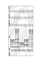
図6及び図7には、上記の実施例と比較例において、20回ごと摩擦試験後の、被膜厚変化の結果が示されている。この結果は、図8にも示した。この結果によれば、図6に示すように、実施例に係る固体表面に形成した膜厚は厚く、強度も高い傾向にあるといえる。一方、図7に示すように、比較例に係る固体表面に形成した膜厚は薄く、強度は低い傾向にあることが分かる。 6 and 7 show the results of changes in film thickness after the friction test every 20 times in the above-described examples and comparative examples. The results are also shown in FIG. According to this result, as shown in FIG. 6, it can be said that the film thickness formed on the solid surface according to the example tends to be thick and strong. On the other hand, as shown in FIG. 7, it can be seen that the film thickness formed on the solid surface according to the comparative example is thin and the strength tends to be low.
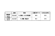
次にまた、図9に示すように、別の実施例45を示す。実施例45はガラス固体にニッケルを蒸着しその後直ちに電解鉄(Fe)を蒸着し、3日間大気放置した固体を用いた。6−ジアリルアミノ−1,3,5−トリアジン−2,4−ジチオール(DA)膜を25nm、次に6−アリルデシルパーフルオロエチルアミノ−1,3,5−トリアジン−2,4−ジチオール(ADF)膜25nmを蒸着して二層膜(DA/ADF膜)を形成した。実施例1と同様に、これを空気中にて150分間、紫外線を照射し重合被膜を得た。光重合率(アルコール不溶率)と三次元化率(THF不溶率)を求めた。 Next, another embodiment 45 is shown as shown in FIG. In Example 45, nickel was vapor-deposited on a glass solid, and electrolytic iron (Fe) was vapor-deposited immediately thereafter. The solid was left in the atmosphere for 3 days. A 6-diallylamino-1,3,5-triazine-2,4-dithiol (DA) film is 25 nm, and then 6-allyldecylperfluoroethylamino-1,3,5-triazine-2,4-dithiol ( A bilayer film (DA / ADF film) was formed by vapor-depositing an ADF) film of 25 nm. In the same manner as in Example 1, this was irradiated with ultraviolet rays for 150 minutes in the air to obtain a polymerized film. The photopolymerization rate (alcohol insolubility) and the three-dimensionalization rate (THF insolubility) were determined.
図9に示す比較例46はガラス固体にニッケルと電解鉄(Fe)を積層蒸着し、真空中でそのまま、DAとADF膜を形成した以外、全て45と同じ重合膜である。
図9には、上記の実施例と比較例において、光重合率と三次元化率が示されている。重合率はDA又はDBの混合物がどの程度重合したかを示す。三次元化率はDAとADFが共重合しているかどうかの目安となる。大気放置して酸化処理をした実施例に係る固体の方が、光重合率、三次元化率が高くなり、共重合していることが分かる。
Comparative Example 46 shown in FIG. 9 is a polymer film that is the same as all 45 except that nickel and electrolytic iron (Fe) are laminated and deposited on a glass solid, and DA and ADF films are formed as they are in vacuum.
FIG. 9 shows the photopolymerization rate and the three-dimensionalization rate in the above-described examples and comparative examples. The polymerization rate indicates how much the mixture of DA or DB has been polymerized. The three-dimensional ratio is a measure of whether DA and ADF are copolymerized. It can be seen that the solid according to the example that was left in the atmosphere and oxidized was higher in photopolymerization rate and three-dimensionalization rate and copolymerized.
本発明によれば、得られる被膜は、種々の製品、例えば、コネクター材料、金属ギア、装飾用金属製晶、金属鏡、金属金型、ハードディスク、磁気テープ、時計の針、金属食器などに応用可能である。
そして、この被膜はトリアジンジチオールの種類を選択することにより、低自由エネルギーから高自由エネルギー表面に変化させることができ、プラスチックスや窓ガラス等セラミックスの表面改質にも有効である。
According to the present invention, the resulting coating is applied to various products such as connector materials, metal gears, decorative metal crystals, metal mirrors, metal molds, hard disks, magnetic tapes, clock hands, metal tableware, etc. Is possible.
This coating can be changed from a low free energy to a high free energy surface by selecting the type of triazinedithiol, and is effective for surface modification of ceramics such as plastics and window glass.
1 るつぼ
2 ヒーター
3 水晶振動子式膜厚計
4 モノマー
5 室
6 シャッター
7 固体
1 Crucible 2
Claims (4)
(CH2 =CH−(CH2 )8 COO(CH2 CH2 ))2 N−,
((CH2 =CH−(CH2 )9 COO(CH2 CH2 ))2−, (C4 F9 COO(CH2 CH2 ))2 N−,
(C6 F13COO(CH2 CH2 ))2 N−,(C8 F17COO(CH2 CH2 ))2 N−,
(C10F21COO(CH2 CH2 ))2 N−である。また、通常MはHとLi,Na,K,Ceなどのアルカリである。〕
で示されるトリアジンジチオール誘導体の1種または2種以上の原料を、固体の表面に真空蒸着法によって混合あるいは積層する高分子薄膜生成方法において、
上記蒸着の前に、上記固体の表面にn型半導体性を示す金属酸化物を形成する酸化処理工程を設けたことを特徴とするトリアジンジチオール誘導体の高分子薄膜生成方法。 General formula on solid surface
(CH 2 = CH- (CH 2 ) 8 COO (CH 2 CH 2)) 2 N-,
((CH 2 = CH- (CH 2) 9 COO (CH 2 CH 2)) 2 -, 2 N- (C 4 F 9 COO (CH 2 CH 2)),
(C 6 F 13 COO (CH 2 CH 2)) 2 N -, 2 N- (C 8 F 17 COO (CH 2 CH 2)),
(C 10 F 21 COO (CH 2 CH 2)) 2 is N-. Usually, M is an alkali such as H and Li, Na, K, and Ce. ]
In a method for producing a polymer thin film in which one or more raw materials of a triazine dithiol derivative represented by the formula (1) are mixed or laminated on a solid surface by a vacuum deposition method,
A method for producing a polymer thin film of a triazine dithiol derivative, comprising an oxidation treatment step of forming a metal oxide exhibiting n-type semiconductivity on the surface of the solid before the vapor deposition.
Priority Applications (1)
| Application Number | Priority Date | Filing Date | Title |
|---|---|---|---|
| JP2004103932A JP4062537B2 (en) | 2004-03-31 | 2004-03-31 | Polymer thin film formation method of triazine dithiol derivative |
Applications Claiming Priority (1)
| Application Number | Priority Date | Filing Date | Title |
|---|---|---|---|
| JP2004103932A JP4062537B2 (en) | 2004-03-31 | 2004-03-31 | Polymer thin film formation method of triazine dithiol derivative |
Publications (2)
| Publication Number | Publication Date |
|---|---|
| JP2005290426A true JP2005290426A (en) | 2005-10-20 |
| JP4062537B2 JP4062537B2 (en) | 2008-03-19 |
Family
ID=35323694
Family Applications (1)
| Application Number | Title | Priority Date | Filing Date |
|---|---|---|---|
| JP2004103932A Expired - Fee Related JP4062537B2 (en) | 2004-03-31 | 2004-03-31 | Polymer thin film formation method of triazine dithiol derivative |
Country Status (1)
| Country | Link |
|---|---|
| JP (1) | JP4062537B2 (en) |
Cited By (4)
| Publication number | Priority date | Publication date | Assignee | Title |
|---|---|---|---|---|
| JP2007131556A (en) * | 2005-11-09 | 2007-05-31 | Iwate Univ | Functional triazine dithiol and method for producing the same |
| JP2007149711A (en) * | 2005-10-29 | 2007-06-14 | Iwate Univ | ORGANIC THIN FILM TRANSISTOR DEVICE, ITS MANUFACTURING METHOD, AND METAL THIN FILM FORMING METHOD |
| KR20150114991A (en) * | 2013-02-06 | 2015-10-13 | 도요보 가부시키가이샤 | Laminate film |
| CN113930817A (en) * | 2021-10-12 | 2022-01-14 | 合肥国轩高科动力能源有限公司 | Treatment method of aluminum shell for lithium ion battery |
-
2004
- 2004-03-31 JP JP2004103932A patent/JP4062537B2/en not_active Expired - Fee Related
Cited By (5)
| Publication number | Priority date | Publication date | Assignee | Title |
|---|---|---|---|---|
| JP2007149711A (en) * | 2005-10-29 | 2007-06-14 | Iwate Univ | ORGANIC THIN FILM TRANSISTOR DEVICE, ITS MANUFACTURING METHOD, AND METAL THIN FILM FORMING METHOD |
| JP2007131556A (en) * | 2005-11-09 | 2007-05-31 | Iwate Univ | Functional triazine dithiol and method for producing the same |
| KR20150114991A (en) * | 2013-02-06 | 2015-10-13 | 도요보 가부시키가이샤 | Laminate film |
| KR102135609B1 (en) * | 2013-02-06 | 2020-07-20 | 도요보 가부시키가이샤 | Laminate film |
| CN113930817A (en) * | 2021-10-12 | 2022-01-14 | 合肥国轩高科动力能源有限公司 | Treatment method of aluminum shell for lithium ion battery |
Also Published As
| Publication number | Publication date |
|---|---|
| JP4062537B2 (en) | 2008-03-19 |
Similar Documents
| Publication | Publication Date | Title |
|---|---|---|
| JP5725541B2 (en) | LAMINATE, MANUFACTURING METHOD THEREOF, ELECTRONIC DEVICE MEMBER AND ELECTRONIC DEVICE | |
| US20100092747A1 (en) | Infrared-reflecting films and method for making the same | |
| US20120258858A1 (en) | Method for deposition by sputtering, resulting product, and sputtering target | |
| EP1116801B1 (en) | Method of applying a coating by physical vapour deposition | |
| JPS5827103B2 (en) | Multilayer coating reflector | |
| JP5221364B2 (en) | Substrate manufacturing method | |
| JP4062537B2 (en) | Polymer thin film formation method of triazine dithiol derivative | |
| TWI604751B (en) | Electronic device and electronic device sealing method | |
| JP2000096212A (en) | Photocatalyst film-coated member and method of manufacturing the same | |
| WO2003106732A1 (en) | Article coated with titanium compound film, process for producing the article and sputtering target for use in the film coating | |
| CN111822001B (en) | A kind of multilayer composite photocatalytic film material and its preparation method and application | |
| CN101305111A (en) | Method for applying a porous glass layer | |
| CN102051497B (en) | Preparation methods of gold and silver embedded target and film thereof | |
| JP3672519B2 (en) | Method for forming thin film of triazine thiol derivative | |
| CN103572233B (en) | A kind of Noble metal ceramic film and preparation method thereof | |
| JP2008106342A (en) | Photocatalytic tungsten oxide thin film | |
| JP2000192237A (en) | Method for producing highly transparent gas barrier film | |
| JP4096606B2 (en) | Method for producing titanium compound film-coated article | |
| EP1624087B1 (en) | A method for depositing thin layers of titanium dioxide on support surfaces | |
| TWI814855B (en) | Transparent conductive film | |
| CN102758184A (en) | Film-coated component and preparation method thereof | |
| JP2002047558A (en) | Metal plate having photocatalytic activity and method for producing the same | |
| CN118241161A (en) | Zirconium-titanium-silver amorphous/silver nano-crystalline multilayer film and preparation method thereof | |
| KR102218282B1 (en) | Method manufacturing stacked structure for printed circuit board comprising ternary-compound and device operating thereof | |
| TWI295325B (en) | An apparatus to deposite a conductive film on the plastic substrate using radio frequency cosputting technology |
Legal Events
| Date | Code | Title | Description |
|---|---|---|---|
| A711 | Notification of change in applicant |
Effective date: 20060516 Free format text: JAPANESE INTERMEDIATE CODE: A712 |
|
| RD02 | Notification of acceptance of power of attorney |
Free format text: JAPANESE INTERMEDIATE CODE: A7422 Effective date: 20060907 |
|
| A977 | Report on retrieval |
Free format text: JAPANESE INTERMEDIATE CODE: A971007 Effective date: 20061020 |
|
| A131 | Notification of reasons for refusal |
Effective date: 20070605 Free format text: JAPANESE INTERMEDIATE CODE: A131 |
|
| A521 | Written amendment |
Free format text: JAPANESE INTERMEDIATE CODE: A523 Effective date: 20070803 |
|
| A131 | Notification of reasons for refusal |
Free format text: JAPANESE INTERMEDIATE CODE: A131 Effective date: 20070828 |
|
| A521 | Written amendment |
Free format text: JAPANESE INTERMEDIATE CODE: A523 Effective date: 20071029 |
|
| TRDD | Decision of grant or rejection written | ||
| A01 | Written decision to grant a patent or to grant a registration (utility model) |
Effective date: 20071127 Free format text: JAPANESE INTERMEDIATE CODE: A01 |
|
| A61 | First payment of annual fees (during grant procedure) |
Free format text: JAPANESE INTERMEDIATE CODE: A61 Effective date: 20071219 |
|
| R150 | Certificate of patent (=grant) or registration of utility model |
Free format text: JAPANESE INTERMEDIATE CODE: R150 |
|
| FPAY | Renewal fee payment (prs date is renewal date of database) |
Year of fee payment: 3 Free format text: PAYMENT UNTIL: 20110111 |
|
| FPAY | Renewal fee payment (prs date is renewal date of database) |
Free format text: PAYMENT UNTIL: 20140111 Year of fee payment: 6 |
|
| FPAY | Renewal fee payment (prs date is renewal date of database) |
Year of fee payment: 6 Free format text: PAYMENT UNTIL: 20140111 |
|
| S531 | Written request for registration of change of domicile |
Free format text: JAPANESE INTERMEDIATE CODE: R313532 |
|
| FPAY | Renewal fee payment (prs date is renewal date of database) |
Free format text: PAYMENT UNTIL: 20140111 Year of fee payment: 6 |
|
| R350 | Written notification of registration of transfer |
Free format text: JAPANESE INTERMEDIATE CODE: R350 |
|
| LAPS | Cancellation because of no payment of annual fees |