JP2005285197A - Semiconductor storage device - Google Patents
Semiconductor storage device Download PDFInfo
- Publication number
- JP2005285197A JP2005285197A JP2004095876A JP2004095876A JP2005285197A JP 2005285197 A JP2005285197 A JP 2005285197A JP 2004095876 A JP2004095876 A JP 2004095876A JP 2004095876 A JP2004095876 A JP 2004095876A JP 2005285197 A JP2005285197 A JP 2005285197A
- Authority
- JP
- Japan
- Prior art keywords
- voltage
- current
- memory cell
- circuit
- node
- Prior art date
- Legal status (The legal status is an assumption and is not a legal conclusion. Google has not performed a legal analysis and makes no representation as to the accuracy of the status listed.)
- Pending
Links
Images


Classifications
-
- G—PHYSICS
- G11—INFORMATION STORAGE
- G11C—STATIC STORES
- G11C11/00—Digital stores characterised by the use of particular electric or magnetic storage elements; Storage elements therefor
- G11C11/56—Digital stores characterised by the use of particular electric or magnetic storage elements; Storage elements therefor using storage elements with more than two stable states represented by steps, e.g. of voltage, current, phase, frequency
- G11C11/5621—Digital stores characterised by the use of particular electric or magnetic storage elements; Storage elements therefor using storage elements with more than two stable states represented by steps, e.g. of voltage, current, phase, frequency using charge storage in a floating gate
- G11C11/5642—Sensing or reading circuits; Data output circuits
-
- G—PHYSICS
- G11—INFORMATION STORAGE
- G11C—STATIC STORES
- G11C16/00—Erasable programmable read-only memories
- G11C16/02—Erasable programmable read-only memories electrically programmable
- G11C16/06—Auxiliary circuits, e.g. for writing into memory
- G11C16/24—Bit-line control circuits
-
- G—PHYSICS
- G11—INFORMATION STORAGE
- G11C—STATIC STORES
- G11C16/00—Erasable programmable read-only memories
- G11C16/02—Erasable programmable read-only memories electrically programmable
- G11C16/06—Auxiliary circuits, e.g. for writing into memory
- G11C16/26—Sensing or reading circuits; Data output circuits
-
- G—PHYSICS
- G11—INFORMATION STORAGE
- G11C—STATIC STORES
- G11C16/00—Erasable programmable read-only memories
- G11C16/02—Erasable programmable read-only memories electrically programmable
- G11C16/06—Auxiliary circuits, e.g. for writing into memory
- G11C16/30—Power supply circuits
-
- G—PHYSICS
- G11—INFORMATION STORAGE
- G11C—STATIC STORES
- G11C5/00—Details of stores covered by group G11C11/00
- G11C5/14—Power supply arrangements, e.g. power down, chip selection or deselection, layout of wirings or power grids, or multiple supply levels
- G11C5/145—Applications of charge pumps; Boosted voltage circuits; Clamp circuits therefor
-
- G—PHYSICS
- G11—INFORMATION STORAGE
- G11C—STATIC STORES
- G11C7/00—Arrangements for writing information into, or reading information out from, a digital store
- G11C7/06—Sense amplifiers; Associated circuits, e.g. timing or triggering circuits
-
- G—PHYSICS
- G11—INFORMATION STORAGE
- G11C—STATIC STORES
- G11C7/00—Arrangements for writing information into, or reading information out from, a digital store
- G11C7/12—Bit line control circuits, e.g. drivers, boosters, pull-up circuits, pull-down circuits, precharging circuits, equalising circuits, for bit lines
-
- G—PHYSICS
- G11—INFORMATION STORAGE
- G11C—STATIC STORES
- G11C2207/00—Indexing scheme relating to arrangements for writing information into, or reading information out from, a digital store
- G11C2207/06—Sense amplifier related aspects
- G11C2207/065—Sense amplifier drivers
-
- G—PHYSICS
- G11—INFORMATION STORAGE
- G11C—STATIC STORES
- G11C2207/00—Indexing scheme relating to arrangements for writing information into, or reading information out from, a digital store
- G11C2207/22—Control and timing of internal memory operations
- G11C2207/2227—Standby or low power modes
-
- G—PHYSICS
- G11—INFORMATION STORAGE
- G11C—STATIC STORES
- G11C2211/00—Indexing scheme relating to digital stores characterized by the use of particular electric or magnetic storage elements; Storage elements therefor
- G11C2211/56—Indexing scheme relating to G11C11/56 and sub-groups for features not covered by these groups
- G11C2211/563—Multilevel memory reading aspects
- G11C2211/5634—Reference cells
-
- G—PHYSICS
- G11—INFORMATION STORAGE
- G11C—STATIC STORES
- G11C2211/00—Indexing scheme relating to digital stores characterized by the use of particular electric or magnetic storage elements; Storage elements therefor
- G11C2211/56—Indexing scheme relating to G11C11/56 and sub-groups for features not covered by these groups
- G11C2211/564—Miscellaneous aspects
- G11C2211/5645—Multilevel memory with current-mirror arrangements
Abstract
Description
この発明は、半導体記憶装置に関し、特に、メモリセルを流れる電流を参照セルを流れる電流と比較してその比較結果に基づいてメモリセルの記憶データを読出す半導体記憶装置に関する。より特定的には、この発明は、不揮発性半導体記憶装置のメモリセルの記憶データを正確に読出すための構成に関する。 The present invention relates to a semiconductor memory device, and more particularly to a semiconductor memory device that compares a current flowing through a memory cell with a current flowing through a reference cell and reads data stored in the memory cell based on the comparison result. More specifically, the present invention relates to a configuration for accurately reading stored data in a memory cell of a nonvolatile semiconductor memory device.
消費電力および発熱量を低減するために、半導体集積回路装置においては、電源電圧が低くされてきている。半導体記憶装置においても、同様、電源電圧が低くされてきている。このような半導体記憶装置の1つの不揮発性半導体記憶装置においては、メモリセルデータの読出しは、電流センス方式のセンスアンプ(電流センスアンプ)を用いて行われる。電流センスアンプは、定電流を供給するカレントミラー段を含み、選択メモリセルの駆動電流と参照セルの駆動電流とを比較し、その比較結果に基づいた内部データを出力し、これにより選択メモリセルのデータを読出す。 In order to reduce power consumption and heat generation, power supply voltages have been lowered in semiconductor integrated circuit devices. Similarly, in semiconductor memory devices, the power supply voltage has been lowered. In one nonvolatile semiconductor memory device of such a semiconductor memory device, reading of memory cell data is performed using a current sense type sense amplifier (current sense amplifier). The current sense amplifier includes a current mirror stage that supplies a constant current, compares the drive current of the selected memory cell with the drive current of the reference cell, and outputs internal data based on the comparison result, thereby selecting the selected memory cell Read the data.
このような電流センスアンプにおいては、正確にセンス動作を行なうためには、カレントミラー段を構成するトランジスタは、飽和領域で動作させる必要がある。飽和領域においては、MOSトランジスタ(絶縁ゲート型電界効果トランジスタ)の場合、次式を満たすことが要求される。 In such a current sense amplifier, it is necessary to operate the transistors constituting the current mirror stage in the saturation region in order to perform the sensing operation accurately. In the saturation region, in the case of a MOS transistor (insulated gate type field effect transistor), it is required to satisfy the following equation.
Vds≧Vgs−Vth
ここで、Vdsはドレイン−ソース間電圧を示し、Vgsはゲート−ソース間電圧を示し、Vthはしきい値電圧を示す。
Vds ≧ Vgs−Vth
Here, Vds indicates a drain-source voltage, Vgs indicates a gate-source voltage, and Vth indicates a threshold voltage.
PチャネルMOSトランジスタでセンスアンプのカレントミラーを構成する場合、ソースに電源電圧が供給され、ドレインに比較結果に応じた電圧が生成される。したがって、上式から明らかなように、電源電圧が低くなる場合、MOSトランジスタを飽和領域で動作させるのが極めて困難となり、高精度でセンス動作を行なうのは困難となる。 When a current mirror of a sense amplifier is constituted by a P-channel MOS transistor, a power supply voltage is supplied to the source and a voltage corresponding to the comparison result is generated at the drain. Therefore, as is apparent from the above equation, when the power supply voltage is low, it is extremely difficult to operate the MOS transistor in the saturation region, and it is difficult to perform the sensing operation with high accuracy.
PチャネルMOSトランジスタは、通常、ゲート電極がN型不純物を導入したポリシリコンで構成され、PチャネルMOSトランジスタの場合、ゲート電極と半導体基板の仕事関数の差により、しきい値電圧の絶対値が大きくなる(N型ゲート電極により電子が半導体基板表面に引き寄せられ、チャネル形成時、反転層ができにくくなる)。このPチャネルMOSトランジスタのしきい値電圧の絶対値を小さくするため、表面に、P型不純物を導入する。このため、半導体基板表面よりも内部にチャネルが形成される。このようなMOSトランジスタが、埋込チャネルMOSトランジスタと呼ばれる。 A P-channel MOS transistor is usually composed of polysilicon with an N-type impurity introduced into the gate electrode. In the case of a P-channel MOS transistor, the absolute value of the threshold voltage is different depending on the work function difference between the gate electrode and the semiconductor substrate. (The electrons are attracted to the surface of the semiconductor substrate by the N-type gate electrode, making it difficult to form an inversion layer when forming a channel) In order to reduce the absolute value of the threshold voltage of this P-channel MOS transistor, a P-type impurity is introduced into the surface. For this reason, a channel is formed inside the semiconductor substrate surface. Such a MOS transistor is called a buried channel MOS transistor.
この埋込チャネルは、ソースおよびドレイン領域と同じ導電型の不純物が添加される領域である。このような埋込チャネル型MOSトランジスタにおいては、基板内部をキャリア(正孔)が通過するため、移動度が大きくなり、しきい値電圧の絶対値低下時のサブスレッショルド特性が劣化し、リーク電流が増加するという問題が生じる。このため、低しきい値化が困難であり、PチャネルMOSトランジスタは、導通状態とするためには、ある程度のゲート−ソース間電圧は必要とされ、低電圧化が、NチャネルMOSトランジスタに比べて困難である。したがって、このような電流センスアンプにおけるカレントミラー段においてPチャネルMOSトランジスタを利用する場合、低電源電圧下では、正確なセンス動作を高精度で行なうことができなくなるという問題が生じる。 The buried channel is a region to which an impurity having the same conductivity type as that of the source and drain regions is added. In such a buried channel MOS transistor, since carriers (holes) pass through the substrate, the mobility is increased, the subthreshold characteristic when the absolute value of the threshold voltage is lowered, and the leakage current is deteriorated. The problem arises that increases. For this reason, it is difficult to lower the threshold value, and the P-channel MOS transistor requires a certain level of gate-source voltage in order to make it conductive, and the lower voltage is lower than that of the N-channel MOS transistor. It is difficult. Therefore, when a P-channel MOS transistor is used in the current mirror stage in such a current sense amplifier, there arises a problem that accurate sensing operation cannot be performed with high accuracy under a low power supply voltage.
このセンス動作を高精度で行なうことを目的とする構成が、特許文献1(特開平4−216397号公報)に示されている。この特許文献1に示される構成においては、差動増幅器とオフセット手段とでセンス回路を構成し、メモリセルアレイのノーマルビット線と参照セルが接続される参照ビット線とに異なる大きさの電流を供給する。この特許文献1は、このオフセット電流を流すことにより、電流オフセット型センスアンプの静的特性および動的特性を、改良することを図る。
A configuration aiming at performing this sensing operation with high accuracy is disclosed in Patent Document 1 (Japanese Patent Laid-Open No. Hei 4-21697). In the configuration disclosed in
また、このような半導体記憶装置においては、動作温度に従ってメモリセルを流れる電流が異なる。メモリセルデータを正確に読出すためには、このような温度特性を補償して、メモリセル電流を検出してデータを読出す必要がある。 In such a semiconductor memory device, the current flowing through the memory cell differs according to the operating temperature. In order to read the memory cell data accurately, it is necessary to compensate for such temperature characteristics and detect the memory cell current to read the data.
このような動作温度の相違に基づくメモリセル電流の温度依存性を補償するための構成が、特許文献2(特表2003−530656号パンフレット)に示されている。この特許文献2においては、プログラム(書込および消去)動作時においてビット線に所定値以上のリーク電流が生じていないかを検証する自動プログラム妨害消去検証(APDEV)動作時のワード線電圧を温度補償する構成が示されている。
A configuration for compensating for the temperature dependence of the memory cell current based on such a difference in operating temperature is shown in Patent Document 2 (Japanese Patent Publication No. 2003-530656 pamphlet). In this
また、メモリセル電流の温度依存性を補償することを図る構成が、特許文献3(特開2003−217287号公報)において示されている。この特許文献3においては、メモリセル電流の温度依存性を、ワード線電圧の温度依存性およびビット線の放電時間の温度依存性とを制御して相殺し、温度依存性の少ないメモリセルのしきい値電圧分布を得ることを図る。
Further, Japanese Patent Application Laid-Open No. 2003-217287 discloses a configuration for compensating for the temperature dependence of the memory cell current. In this
また、同様、メモリセルのしきい値電圧分布の温度依存性を低減することを図る構成が、特許文献4(特開2001−35177号公報)に示されている。この特許文献4に示される構成においては、温度依存性を有する電流を発生する電流源と温度に依存しない一定の電流を生成する電流源とを用い、これらの電流源を選択的に用いて、温度特性を正および負両方ともに調整することを図っている。
特許文献1に示される構成においては、ノーマルメモリセルが接続されるノーマルビット線と参照セルが接続される参照ビット線に対し、供給する電流をアンバランスとすることにより、負荷アンバランス型センス回路と同様の特性を実現し、また、この負荷アンバランス型センス回路の電源電圧に対する制限をなくすことを図る。
In the configuration shown in
しかしながら、この特許文献1に示される構成においては、常時、ノーマルビット線および参照ビット線にアンバランスな電流を供給しており、選択的に、ノーマルビット線のみまたは参照ビット線のみに負荷電流を供給して、メモリセル特性の検証を行なうことはできない。
However, in the configuration shown in
特許文献2に示される構成においては、P型抵抗素子およびN型抵抗素子の抵抗値の温度依存性の異なることを利用して、これらのP型抵抗素子およびN型抵抗素子を選択的に組合せて、動作温度に応じて抵抗値の予め定められた傾きを生成して、ワード線印加電圧の温度補償を行なっている。したがって、この特許文献2に示される構成においては、温度に応じて、P型抵抗素子およびN型抵抗素子の組合せを、適応的に調節する必要があり、その温度制御が困難であるという問題が生じる。
In the configuration shown in
特許文献3に示される構成においても、ワード線電圧に温度依存性を持たせることにより、メモリセル電流の温度依存性を相殺している。しかしながら、この特許文献3に示される構成においては、ノーマルメモリセルおよび参照メモリセルの特性の温度依存性が異なる場合については何ら考慮してない。
Also in the configuration shown in
特許文献4に示される構成においても、同様、メモリセル電流の温度依存性を補償するために、ワード線電圧に、メモリセル電流の温度依存性を相殺するような温度依存性を持たせている。しかしながら、この特許文献4においても、ノーマルメモリセルと参照メモリセルの駆動電流の温度依存性が異なる場合については、何ら考察していない。 Similarly, in the configuration disclosed in Patent Document 4, in order to compensate for the temperature dependence of the memory cell current, the word line voltage has a temperature dependence that cancels the temperature dependence of the memory cell current. . However, even in this Patent Document 4, no consideration is given to the case where the temperature dependence of the drive currents of the normal memory cell and the reference memory cell is different.
また、これらの特許文献1から4においては、内部電源電圧低下時においても、高精度でセンス動作を行なうためのセンスアンプの構成およびセンス動作については考察していない。
Further, these
それゆえ、この発明の目的は、低電源電圧下においても、正確にメモリセルデータを読出すことのできる半導体記憶装置を提供することである。 SUMMARY OF THE INVENTION An object of the present invention is to provide a semiconductor memory device that can accurately read memory cell data even under a low power supply voltage.
この発明の他の目的は、多値データを高精度で読出すことのできる電流センスアンプを備える半導体記憶装置を提供することである。 Another object of the present invention is to provide a semiconductor memory device including a current sense amplifier capable of reading multi-value data with high accuracy.
この発明のさらに他の目的は、動作環境の影響を受けることなく正確にメモリセルデータの読出を行うことのできる不揮発性半導体記憶装置を提供することである。 Still another object of the present invention is to provide a nonvolatile semiconductor memory device capable of accurately reading memory cell data without being affected by the operating environment.
この発明の第1の観点に係る半導体記憶装置は、複数のメモリセルと、複数のメモリセルの選択メモリセルのデータを検出するセンス増幅回路を備える。このセンス増幅回路は、内部電源電圧よりも高い電圧を受ける昇圧電源ノードと、この昇圧電源ノードに動作時結合され、メモリセルを流れる電流に応じてメモリセルの記憶データを読出す読出部と、この内部電源電圧を受けるノードに結合され、プリチャージ指示信号に応答してメモリセルへ内部電源ノードからの電流を供給して選択メモリセルが接続されるデータ線を所定電位にプリチャージするプリチャージ段とを含む。 A semiconductor memory device according to a first aspect of the present invention includes a plurality of memory cells and a sense amplifier circuit that detects data of a selected memory cell of the plurality of memory cells. The sense amplifier circuit includes a boost power supply node that receives a voltage higher than the internal power supply voltage, a reading unit coupled to the boost power supply node in operation and reading stored data of the memory cell in response to a current flowing through the memory cell; A precharge coupled to a node receiving the internal power supply voltage and supplying a current from the internal power supply node to the memory cell in response to a precharge instruction signal to precharge a data line connected to the selected memory cell to a predetermined potential. Including steps.
この発明の第2の観点に係る半導体記憶装置は、各々がゲートを有し、そのしきい値電圧によりデータを記憶するトランジスタで構成される複数のメモリセルと、これらのメモリセルと同一構造を有する参照セルと、複数のメモリセルの選択メモリセルの駆動電流と参照セルの駆動電流をセンスして選択メモリセルのデータを読出すセンス増幅回路と、参照セルおよび選択メモリセルのゲートに印加する電圧を生成するゲート電圧発生回路を備える。このゲート電圧発生回路は、選択メモリセルの通常データ読出モード時には参照セルおよび選択メモリセルのゲートに対する電圧として同一レベルの電圧を生成し、選択メモリセルの書込または消去の検証モード時には、メモリセルの駆動電流分布範囲の上下端の位置のメモリセルについては、通常モード時と異なるレベルの電圧を選択メモリセルのゲート電圧として生成する。 A semiconductor memory device according to a second aspect of the present invention includes a plurality of memory cells each having a gate and configured by transistors that store data by the threshold voltage, and the same structure as these memory cells. A reference cell having a plurality of memory cells, a sense amplifier circuit that senses a drive current of a selected memory cell of a plurality of memory cells and a drive current of the reference cell and reads data of the selected memory cell; A gate voltage generation circuit for generating a voltage is provided. This gate voltage generating circuit generates a voltage of the same level as the voltage for the reference cell and the gate of the selected memory cell in the normal data read mode of the selected memory cell, and in the verification mode for writing or erasing the selected memory cell For the memory cells at the upper and lower ends of the driving current distribution range, a voltage of a level different from that in the normal mode is generated as the gate voltage of the selected memory cell.
この発明の第3の観点に係る半導体記憶装置は、複数のメモリセルと、参照メモリセルと、複数のメモリセルの選択メモリセルに接続される第1のノードと参照セルに接続される第2のノードとを有し、これらの第1および第2のノードを流れる電流に従って選択メモリセルのデータを読出すセンス増幅器を備える。この第1のノードの容量値は、第2のノードの容量値よりも大きくされる。 A semiconductor memory device according to a third aspect of the present invention includes a plurality of memory cells, a reference memory cell, a first node connected to a selected memory cell of the plurality of memory cells, and a second node connected to the reference cell. And a sense amplifier that reads data of a selected memory cell in accordance with currents flowing through the first and second nodes. The capacity value of the first node is made larger than the capacity value of the second node.
この発明の第4の観点に係る半導体記憶装置は、選択メモリセルに接続される第1のノードと参照セルに接続される第2のノードとを有し、第1および第2のノードを流れる電流に従って選択メモリセルのデータを検出するセンス増幅回路と、これら第1および第2のノードにそれぞれ結合され、活性化時、定電流をこれらの第1および第2のノードから駆動する第1および第2の定電流源を備える。これらの第1および第2の定電流源は個別に活性化することができる。 A semiconductor memory device according to a fourth aspect of the present invention has a first node connected to a selected memory cell and a second node connected to a reference cell, and flows through the first and second nodes. A sense amplifier circuit for detecting data of a selected memory cell according to a current, and a first and a second node coupled to the first and second nodes, respectively, for driving a constant current from the first and second nodes when activated. A second constant current source is provided. These first and second constant current sources can be activated individually.
この発明の第5の観点に係る半導体記憶装置は、少なくとも1行に整列して配置され、各々がゲートを有しかつそのゲート電圧/駆動電流特性が温度依存性を有するトランジスタを含み、このトランジスタのしきい値電圧に応じてデータを記憶するメモリセルと、メモリセルのトランジスタのゲート電圧/駆動電流特性の温度依存性を補償する温度依存性を有するワード線駆動電圧を発生する電圧発生回路と、行に整列して配置されるメモリセルに対応して配置され、メモリセルトランジスタのゲートが接続される少なくとも1本のワード線と、この1本のワード線の選択時、電圧発生回路の発生するワード線駆動電圧を1本のワード線に伝達するワード線選択回路を備える。この電圧発生回路からのワード線駆動電圧は、制御信号に従って、正および負の温度依存性のいずれをも有することが可能である。 A semiconductor memory device according to a fifth aspect of the present invention includes transistors arranged in at least one row, each having a gate, and having a gate voltage / drive current characteristic having temperature dependency. A memory cell for storing data in accordance with the threshold voltage of the memory, and a voltage generation circuit for generating a word line drive voltage having a temperature dependency for compensating the temperature dependency of the gate voltage / drive current characteristics of the transistor of the memory cell At least one word line arranged corresponding to the memory cells arranged in alignment with the row and connected to the gate of the memory cell transistor, and generation of the voltage generation circuit when this one word line is selected A word line selection circuit for transmitting a word line driving voltage to be transmitted to one word line. The word line drive voltage from the voltage generation circuit can have both positive and negative temperature dependence according to the control signal.
第1の観点の半導体記憶装置においては、センス増幅回路の電源電圧として、内部電源電圧よりも高い電圧を供給している。したがって、内部電源電圧が低電圧化される場合においても、その読出部を構成するトランジスタを飽和領域で動作させることができ、安定に、センス動作を行なうことができる。 In the semiconductor memory device of the first aspect, a voltage higher than the internal power supply voltage is supplied as the power supply voltage of the sense amplifier circuit. Therefore, even when the internal power supply voltage is lowered, the transistor constituting the reading unit can be operated in the saturation region, and the sensing operation can be performed stably.
第2の観点に係る半導体記憶装置においては、メモリセルの駆動電流分布範囲の上下端の位置のメモリセルの検証時には、そのゲート電圧を通常動作モード時と異なる電圧レベルに設定しており、メモリセルのしきい値電圧分布を高精度に制御することができ、多値データ記憶時においても、正確に、データの読出を行なうことができる。 In the semiconductor memory device according to the second aspect, when verifying the memory cells at the upper and lower positions of the drive current distribution range of the memory cell, the gate voltage is set to a voltage level different from that in the normal operation mode. The threshold voltage distribution of the cell can be controlled with high accuracy, and data can be read accurately even when multi-value data is stored.
この発明の第3の観点に係る半導体記憶装置においては、参照セルが接続する第2のノードの容量値が、ノーマルメモリセルが接続される第1のノードよりも小さくされており、この容量値のアンバランスにより、センスノードの電圧を高速で所定電圧レベルに収束させることができ、アクセス時間を短縮することができる。 In the semiconductor memory device according to the third aspect of the present invention, the capacitance value of the second node to which the reference cell is connected is made smaller than that of the first node to which the normal memory cell is connected. By this unbalance, the voltage of the sense node can be converged to a predetermined voltage level at high speed, and the access time can be shortened.
この発明の第4の観点に係る半導体記憶装置においては、参照セルおよびノーマルセルに結合されるセンスノードそれぞれに、活性化時定電流を駆動する定電流源を接続しており、メモリセルおよび参照セルをそれぞれ独立に、電流特性を検証することができる。 In the semiconductor memory device according to the fourth aspect of the present invention, a constant current source for driving a constant current at the time of activation is connected to each sense node coupled to the reference cell and the normal cell. The current characteristics can be verified independently for each cell.
この発明の第5の観点に係る半導体記憶装置においては、メモリセルのトランジスタのゲート電圧とその駆動電流との間の特性の温度依存性を補償する温度依存性を有するワード線駆動電圧を発生し、このワード線駆動電圧は、制御信号により正および負の温度依存性を有することが可能である。したがって、最適な電圧レベルに、動作温度に応じてワード線駆動電圧を設定することができ、メモリセルトランジスタを流れる電流の温度依存性を補償することができる。これにより、参照メモリセルとメモリセルのしきい値電圧の温度依存性が異なる場合においても、正確に、メモリセル電流を、温度依存性を持たせることなく生成することができ、正確なセンス動作が保証される。 In the semiconductor memory device according to the fifth aspect of the present invention, a word line drive voltage having a temperature dependency for compensating the temperature dependency of the characteristics between the gate voltage of the transistor of the memory cell and its drive current is generated. The word line drive voltage can have positive and negative temperature dependencies depending on the control signal. Therefore, the word line driving voltage can be set to the optimum voltage level according to the operating temperature, and the temperature dependence of the current flowing through the memory cell transistor can be compensated. As a result, even when the temperature dependency of the threshold voltage of the reference memory cell and that of the memory cell are different, the memory cell current can be generated accurately without having the temperature dependency, and the accurate sensing operation can be performed. Is guaranteed.
[実施の形態1]
図1は、この発明の実施の形態1に従う不揮発性半導体記憶装置の要部の構成を概略的に示す図である。図1において、この発明の実施の形態1に従う不揮発性半導体記憶装置は、行列状に配列される不揮発性メモリセルを有するメモリセルアレイ1を含む。メモリセルアレイ1においては、メモリセル行に対応してワード線が配置され、また、メモリセル列に対応してビット線が配置される。しかしながら、図1においては、図面を簡略化するために、これらのワード線およびビット線は、示していない。
[Embodiment 1]
FIG. 1 schematically shows a structure of a main portion of the nonvolatile semiconductor memory device according to the first embodiment of the present invention. 1, the nonvolatile semiconductor memory device according to the first embodiment of the present invention includes a
不揮発性半導体記憶装置は、さらに、メモリセルアレイ1のアドレス指定された行を選択しかつ選択行のワード線を所定の電圧レベルへ駆動する行選択駆動回路2と、メモリセルアレイ1の列(ビット線)を選択する列選択回路3と、データ読出時、列選択回路3により選択された列上のメモリセルのデータを読出す読出回路4と、この不揮発性半導体記憶装置の各種の内部動作を制御する制御回路5と、制御回路5の制御の下に、データの書込/消去および読出に必要な内部電圧Vwを生成しかつ読出回路4に対する昇圧電圧Vbsを供給する内部電圧発生回路6を含む。
The nonvolatile semiconductor memory device further includes a row
制御回路5は、内部電源電圧VCCを動作電源電圧として受け、また、内部電圧発生回路6は、外部からの電源電圧VEXを動作電源電圧として受ける。この外部電源電圧VEXは、内部電源電圧VCCと同一電圧レベルであってもよく、また、異なる電圧レベルであってもよい。読出回路4へは、また内部電源電圧VCCが与えられる。
メモリセルアレイ1においては、データを記憶するノーマルメモリセル(以下、単にメモリセルと称す)と選択メモリセルのデータ読出時の参照電流を供給する参照セルが配置される。読出回路4は、データ読出時、選択メモリセルと参照セルの駆動電流を比較し、その比較結果に基づいて読出データRDを生成する。
In
列選択回路3は、列アドレス信号をデコードする列アドレスデコーダと、列アドレスデコーダからの列選択信号(およびブロック選択信号)とにしたがって選択列のビット線を読出回路4に接続する列選択ゲートを含む。
制御回路5は、たとえばコマンドデコーダで構成され、外部から与えられる動作モード指示に従って各種動作制御信号を生成する。図1においては、この制御回路5は内部電圧発生回路6および行選択駆動回路2の動作を制御するように示すが、この制御回路5は、また読出回路4におけるデータ読出動作をも制御し、また、列選択回路3に含まれる列アドレスデコード回路の動作および印加電圧レベルをも制御する。
The
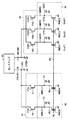
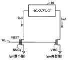
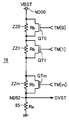
図2は、図1に示す読出回路4に含まれるセンスアンプ(センス増幅回路)の構成の一例を示す図である。図2において、センスアンプは、昇圧電源ノードND1と内部ノードND2の間に接続されかつそのゲートにセンス活性化信号♯SEを受けるPチャネルMOSトランジスタPQ1と、内部ノードND2と内部ノードREFNとの間に接続されかつそのゲートが内部ノードREFNに接続されるPチャネルMOSトランジスタPQ2と、内部ノードND2と内部ノードCELNの間に接続されかつそのゲートが内部ノードREFNに接続されるPチャネルMOSトランジスタPQ3と、プリチャージ指示信号♯PCの活性化時導通し、内部ノードREFNへ内部電源ノードND3からプリチャージ電流Ipgを供給するPチャネルMOSトランジスタPQ4と、プリチャージ指示信号♯PCの活性化時導通し、内部電源ノードND4から内部ノードCELNへプリチャージ電流Ipgを供給するPチャネルMOSトランジスタPQ5を含む。 FIG. 2 is a diagram showing an example of the configuration of a sense amplifier (sense amplifier circuit) included in readout circuit 4 shown in FIG. Referring to FIG. 2, the sense amplifier is connected between boosted power supply node ND1 and internal node ND2, and receives a sense activation signal #SE at its gate, between internal node ND2 and internal node REFN. P channel MOS transistor PQ2 having its gate connected to internal node REFN, and P channel MOS transistor PQ3 having its gate connected to internal node REFN and connected between internal node ND2 and internal node CELN, Conductive when precharge instruction signal #PC is activated, and conducts when P channel MOS transistor PQ4 supplying precharge current Ipg from internal power supply node ND3 to internal node REFN and precharge instruction signal #PC are activated, Internal from internal power supply node ND4 To over de CELN including P-channel MOS transistor PQ5 supplying precharge current Ipg.
電源ノードND3およびND4へは、内部電源電圧VCCが供給される。一方、昇圧電源ノードND1へは、内部電源電圧VCCよりも高い昇圧電圧Vbsが供給される。プリチャージ電力Ipgを、内部電源電圧VCCから生成する。昇圧電圧Vbsは、このセンスアンプのセンス動作においてのみ利用される。これにより、昇圧電圧Vbsを発生する回路の消費電流を低減し、電流消費の増大を抑制する。 Internal power supply voltage VCC is supplied to power supply nodes ND3 and ND4. On the other hand, boosted voltage Vbs higher than internal power supply voltage VCC is supplied to boosted power supply node ND1. Precharge power Ipg is generated from internal power supply voltage VCC. Boosted voltage Vbs is used only in the sense operation of this sense amplifier. As a result, the current consumption of the circuit that generates the boosted voltage Vbs is reduced and the increase in current consumption is suppressed.
これらのPチャネルMOSトランジスタPQ1−PQ5は、その構成は後に説明するが、通常の埋込チャネル方式のPチャネルMOSトランジスタで構成される。 These P channel MOS transistors PQ1 to PQ5 are constituted by ordinary buried channel type P channel MOS transistors, the configuration of which will be described later.
センスアンプは、さらに、内部ノードREFNと内部読出データ線REFBDの間に接続されかつそのゲートに一定のバイアス電圧Vbiasを受けるNチャネルMOSトランジスタNQ1と、内部ノードCELNと内部読出データ線(センスノード)CELBDの間に接続されかつそのゲートにバイアス電圧Vbiasを受けるNチャネルMOSトランジスタNQ2と、センスアンプ活性化信号♯SE2の非活性化時導通し、参照データ線REFBDを接地電圧レベルに維持するNチャネルMOSトランジスタNQ3と、センスアンプ活性化信号♯SE2の非活性化時導通し、内部読出データ線CELBDを接地電圧レベルに維持するNチャネルMOSトランジスタNQ4と、相補イコライズ指示信号EQおよび♯EQの活性化時導通し、内部ノードREFNおよびCELNを電気的に短絡するCMOSトランスミッションゲートTX1と、相補イコライズ指示信号EQおよび♯EQの活性化時導通し、参照データ線REFBDおよび内部読出データ線CELBDを電気的に短絡するCMOSトランスミッションゲートTX2を含む。 Sense amplifier is further connected between internal node REFN and internal read data line REFBD, and has N-channel MOS transistor NQ1 receiving a constant bias voltage Vbias at its gate, internal node CELN and internal read data line (sense node). N-channel MOS transistor NQ2 connected between CELBD and receiving bias voltage Vbias at its gate is turned on when sense amplifier activation signal # SE2 is inactive, and N-channel maintains reference data line REFBD at the ground voltage level N channel MOS transistor NQ4 which conducts when MOS transistor NQ3 is inactive when sense amplifier activation signal # SE2 is inactive and maintains internal read data line CELBD at the ground voltage level, and activation of complementary equalize instruction signals EQ and #EQ When conducting, CMOS transmission gate TX1 that electrically short-circuits local nodes REFN and CELN, and CMOS transmission that conducts when complementary equalize instruction signals EQ and #EQ are activated and electrically short-circuits reference data line REFBD and internal read data line CELBD Includes gate TX2.
参照データ線REFBDは、データ読出時、参照セルRMCに参照ビット線RBLを介して接続され、また、内部読出データ線CELBDは、データ読出時、ビット線BLを介してメモリセル(ノーマルメモリセル)NMCに接続される。これらの参照セルRMCおよびメモリセルNMCのゲートは、共通にワード線WLに接続される。なお、図2においては、このメモリセルおよび参照セルを選択するためのコラム選択ゲート(列選択回路3内に含まれる)は示していない。 Reference data line REFBD is connected to reference cell RMC via reference bit line RBL during data reading, and internal read data line CELBD is a memory cell (normal memory cell) via bit line BL during data reading. Connected to NMC. The gates of these reference cell RMC and memory cell NMC are commonly connected to a word line WL. In FIG. 2, a column selection gate (included in the column selection circuit 3) for selecting the memory cell and the reference cell is not shown.
図3は、図2に示すセンスアンプの動作を示すタイミング図である。以下、図2に示すセンスアンプの動作を、図3に示すタイミング図を参照して説明する。 FIG. 3 is a timing chart showing the operation of the sense amplifier shown in FIG. The operation of the sense amplifier shown in FIG. 2 will be described below with reference to the timing chart shown in FIG.
時刻t1以前においては、センスアンプは非活性状態にあり、センスアンプ活性化信号♯SE2、プリチャージ指示信号♯PC、センス活性化信号♯SEおよびイコライズ指示信号♯EQはHレベルであり、イコライズ指示信号EQがLレベルである。この状態においては、PチャネルMOSトランジスタPQ1が非導通状態にあり、内部ノードND2はフローティング状態にある。また、プリチャージ用のPチャネルMOSトランジスタPQ4およびPQ5もオフ状態にある。NチャネルMOSトランジスタNQ3およびNQ4がオン状態にあり、参照データ線REFBDおよび内部読出データ線CELBDは接地電圧レベルに維持される。またCMOSトランスミッションゲートTX1およびTX2がオン状態であり、内部ノードREFNおよびCELNが電気的に短絡され、また、参照データ線REFBDおよび内部読出データ線CELBDが電気的に短絡されて同一電位に維持される。 Before time t1, the sense amplifier is in an inactive state, and sense amplifier activation signal # SE2, precharge instruction signal #PC, sense activation signal #SE and equalize instruction signal #EQ are at the H level, and equalize instruction Signal EQ is at L level. In this state, P channel MOS transistor PQ1 is in a non-conductive state, and internal node ND2 is in a floating state. Precharge P-channel MOS transistors PQ4 and PQ5 are also off. N channel MOS transistors NQ3 and NQ4 are on, and reference data line REFBD and internal read data line CELBD are maintained at the ground voltage level. Further, CMOS transmission gates TX1 and TX2 are on, internal nodes REFN and CELN are electrically short-circuited, and reference data line REFBD and internal read data line CELBD are electrically short-circuited and maintained at the same potential. .
時刻t1において、内部データの読出動作が開始される。この時刻t1においてイコライズ指示信号EQがHレベル、補のイコライズ指示信号♯EQがLレベルとなり、CMOSトランスミッションゲートTX1およびTX2がオフ状態となり、内部ノードのイコライズが完了する。また、センスアンプ活性化信号♯SE2がLレベルとなり、NチャネルMOSトランジスタNQ3およびNQ4がオフ状態となり、データ線REFBDおよびCELBDの接地電位レベルへのプリチャージが完了する。 At time t1, the internal data reading operation is started. At time t1, equalize instruction signal EQ is at H level, complementary equalize instruction signal #EQ is at L level, CMOS transmission gates TX1 and TX2 are turned off, and equalization of the internal nodes is completed. Sense amplifier activation signal # SE2 attains L level, N channel MOS transistors NQ3 and NQ4 are turned off, and precharging of data lines REFBD and CELBD to the ground potential level is completed.
さらに、この時刻t1において、プリチャージ指示信号♯PCがLレベルとなり、PチャネルMOSトランジスタPQ4およびPQ5がオン状態となり、プリチャージ電流Ipgが、それぞれ参照データ線REFBDおよび内部読出データ線CELBDへ供給される。これらの参照データ線REFBDおよび内部読出データ線CELBDは、それぞれ、図示しない列選択ゲートを介して参照セルRMCおよび選択メモリセルNMCに結合され、これらのプリチャージ電流Ipgが、参照ビット線RBLおよびビット線BLに供給される。 At time t1, precharge instruction signal #PC attains L level, P channel MOS transistors PQ4 and PQ5 are turned on, and precharge current Ipg is supplied to reference data line REFBD and internal read data line CELBD, respectively. The Reference data line REFBD and internal read data line CELBD are coupled to reference cell RMC and selected memory cell NMC via a column selection gate (not shown), and precharge current Ipg is connected to reference bit line RBL and bit line RBL. Supplied to the line BL.
バイアス電圧Vbiasをゲートに受けるNチャネルMOSトランジスタNQ1およびNQ2が、ソースフォロアモードで動作し、この参照データ線REFBDおよび内部読出データ線CELBDの電圧レベルが、一定電圧レベル(Vbias−VTHN:VTHNは、NチャネルMOSトランジスタのしきい値電圧)に維持される。一方、内部ノードREFNおよびCELNは、このプリチャージ電流Ipgにより、内部電源電圧VCCレベルにまで充電される。これらのMOSトランジスタNQ1およびNQ2により、内部ノードREFNおよびCELNは、容量的にデータ線REFBDおよびCELBDから分離され、データ線REFBDおよびCELBDの電位レベルの変動の影響を受けない。 N channel MOS transistors NQ1 and NQ2 receiving bias voltage Vbias at their gates operate in a source follower mode, and reference data line REFBD and internal read data line CELBD are at a constant voltage level (Vbias−VTHN: VTHN is N channel MOS transistor threshold voltage). On the other hand, internal nodes REFN and CELN are charged to internal power supply voltage VCC level by precharge current Ipg. By these MOS transistors NQ1 and NQ2, internal nodes REFN and CELN are capacitively separated from data lines REFBD and CELBD, and are not affected by fluctuations in potential levels of data lines REFBD and CELBD.
時刻t2において、プリチャージ指示信号♯PCがHレベルとなり、MOSトランジスタPQ4およびPQ5がオフ状態となり、内部ノードREFNおよびCELNのプリチャージならびに参照ビット線RBLおよびビット線BLの所定電位へのプリチャージが完了する。 At time t2, precharge instruction signal #PC attains an H level, MOS transistors PQ4 and PQ5 are turned off, internal nodes REFN and CELN are precharged, and reference bit line RBL and bit line BL are precharged to a predetermined potential. Complete.
また、時刻t2において、センス活性化信号♯SEがLレベルとなり、PチャネルMOSトランジスタPQ1がオン状態となり、センスアンプが活性化され、PチャネルMOSトランジスタPQ2およびPQ3が、昇圧ノードND1から電流を供給する。MOSトランジスタPQ2およびPQ3は、MOSトランジスタPQ2をマスタとするカレントミラー段を構成し、同じ大きさの電流を供給する。 At time t2, sense activation signal #SE attains L level, P channel MOS transistor PQ1 is turned on, the sense amplifier is activated, and P channel MOS transistors PQ2 and PQ3 supply current from boosting node ND1. To do. MOS transistors PQ2 and PQ3 form a current mirror stage having MOS transistor PQ2 as a master, and supply currents of the same magnitude.
このとき、まだイコライズ指示信号EQおよび♯EQはそれぞれHレベルおよびLレベルであり、CMOSトランスミッションゲートTX1およびTX2がオン状態である。したがって、内部ノードREFNおよびCELNが、参照セルRMCおよびメモリセルNMCの駆動電流IrefおよびIcelに応じて、同一電圧レベルでそれらの電圧レベルが低下する。 At this time, equalize instruction signals EQ and #EQ are still at the H level and the L level, respectively, and CMOS transmission gates TX1 and TX2 are on. Therefore, internal nodes REFN and CELN decrease in voltage level at the same voltage level in accordance with drive currents Iref and Icel of reference cell RMC and memory cell NMC.
時刻t3において、イコライズ指示信号EQおよび♯EQがそれぞれLレベルおよびHレベルとなり、CMOSトランスミッションゲートTX1およびTX2がオフ状態となる。このときには、内部ノードREFNおよびCELNの電圧レベルは十分低下しており、MOSトランジスタPQ2およびPQ3は、十分に飽和領域で動作し、そのカレントミラー動作により、参照セルRMCに対する参照電流Irefと同じ大きさの電流が、内部ノードCELNへ供給される。この参照電流IrefとメモリセルNMCの駆動電流Icelの差に応じて、内部ノードCELNおよびREFNの間に電位差が高速で生じる。 At time t3, equalize instruction signals EQ and #EQ attain L level and H level, respectively, and CMOS transmission gates TX1 and TX2 are turned off. At this time, the voltage levels of internal nodes REFN and CELN are sufficiently lowered, and MOS transistors PQ2 and PQ3 operate sufficiently in the saturation region, and have the same magnitude as reference current Iref for reference cell RMC by the current mirror operation. Current is supplied to the internal node CELN. In accordance with the difference between this reference current Iref and drive current Icel of memory cell NMC, a potential difference is generated between internal nodes CELN and REFN at high speed.
時刻t4において、センス活性化信号♯SEおよびセンスアンプ活性化信号SE2がともにHレベルとなり、PチャネルMOSトランジスタPQ1がオフ状態、MOSトランジスタNQ3およびNQ4がオン状態となり、センス動作が完了し、データ線REFBDおよびCELBDが再び、接地電圧レベルにプリチャージされる。このデータ線REFBDおよびCELBDの接地電圧レベルへの駆動により、MOSトランジスタNQ1およびNQ2を介して、内部ノードREFNおよびCELNも、接地電圧レベルに放電されて、これらの内部ノードREFNおよびCELNも接地電圧レベルにプリチャージされる。 At time t4, sense activation signal #SE and sense amplifier activation signal SE2 both attain H level, P-channel MOS transistor PQ1 is turned off, MOS transistors NQ3 and NQ4 are turned on, and the sensing operation is completed. REFBD and CELBD are again precharged to the ground voltage level. By driving data lines REFBD and CELBD to the ground voltage level, internal nodes REFN and CELN are also discharged to the ground voltage level via MOS transistors NQ1 and NQ2, and these internal nodes REFN and CELN are also ground voltage level. Is precharged.
CMOSトランスミッションゲートTX1およびTX2を用いて、センス動作時、内部ノードREFNおよびCELNをイコライズしつつ参照電流Irefおよびセル電流Icelを供給することにより、メモリセルNMCの駆動電流のカレントミラー段を構成するPチャネルMOSトランジスタPQ2およびPQ3が十分飽和領域で動作させることができ、最も感度の高い領域で高速でセンス動作を行なうことができる。 The CMOS transmission gates TX1 and TX2 are used to supply the reference current Iref and the cell current Icel while equalizing the internal nodes REFN and CELN during the sensing operation, thereby forming the current mirror stage of the drive current of the memory cell NMC. Channel MOS transistors PQ2 and PQ3 can be operated in a sufficiently saturated region, and a sensing operation can be performed at high speed in the most sensitive region.
内部ノードREFNおよびCELNの電位変化は、MOSトランジスタNQ1およびNQ2の機能により、内部データ線REFBDおよびCELBDへは伝達されない。すなわち、MOSトランジスタNQ1およびNQ2により、内部ノードREFNおよびCELNは、データ線REFBDおよびCELBDと容量的に分離されており、セル電流Icelおよび参照電流Irefの大きさに応じて、内部ノードCELNおよびREFNに高速で電位変化を生じさせることができる。 The potential change of internal nodes REFN and CELN is not transmitted to internal data lines REFBD and CELBD due to the functions of MOS transistors NQ1 and NQ2. That is, the internal nodes REFN and CELN are capacitively separated from the data lines REFBD and CELBD by the MOS transistors NQ1 and NQ2, and the internal nodes CELN and REFN are connected to the internal nodes CELN and REFN according to the magnitudes of the cell current Icel and the reference current Iref. A potential change can be generated at high speed.
図4は、図2に示されるセンスアンプに含まれるPチャネルMOSトランジスタの断面構造を概略的に示す図である。図4において、PチャネルMOSトランジスタは、N型半導体基板領域(たとえばウェルまたは基板)7Aと、この半導体基板領域7A表面に間をおいて形成されるP型不純物領域7Bおよび7Cと、これらの不純物領域7Bおよび7Cの間の基板領域表面に形成されるP型不純物ドープ層9Aと、この不純物ドープ層9A上に図示しないゲート絶縁膜を介して形成されるゲート電極8を含む。このゲート電極8は、通常、N型不純物をドープした多結晶シリコンで構成される。
FIG. 4 schematically shows a cross-sectional structure of a P-channel MOS transistor included in the sense amplifier shown in FIG. In FIG. 4, a P-channel MOS transistor includes an N-type semiconductor substrate region (for example, well or substrate) 7A, P-
この図4に示すPチャネルMOSトランジスタにおいては、ゲート電極8が、N型半導体であり、この半導体基板領域7A表面の電子が、ゲート電極層8方向へ移動する。この半導体基板領域10表面の電子の影響を相殺するために、P型不純物ドープ層9Aを設ける。この場合、チャネル領域9Bは、このP型不純物ドープ層9A下部に形成され、埋込チャネルを形成する。この埋込チャネル9Aにおいては、ゲート電極8にソース領域(不純物領域7Bまたは7C)の電圧レベルよりも低い電圧レベルを印加することにより、電子が半導体基板領域7A表面から下部へ移動し、空乏層が広がり、埋込チャネル領域9Bに、反転層が形成され、このPチャネルMOSトランジスタがオン状態となる。
In the P-channel MOS transistor shown in FIG. 4,
この図4に示す埋込チャネル方式のPチャネルMOSトランジスタにおいては、P型不純物ドープ層9Aが設けられており、このため、オフリーク電流が流れるため、しきい値電圧の絶対値を十分に小さくすることができない。また、しきい値電圧の絶対値がNMOSトランジスタと比べて大きく、また、多数キャリアも質量の大きいホールであり、その電流駆動力もNチャネルMOSトランジスタと比べて小さい。したがって、PチャネルMOSトランジスタを利用する場合、一般的には、チャネル幅を広くして、電流駆動力を大きくする対策がとられる。しかしながら、この昇圧電圧Vbsを用いることにより、内部電源電圧VCCが低い場合においても、センスアンプ動作時、このカレントミラー段を構成するPチャネルMOSトランジスタPQ2およびPQ3およびPQ1を飽和領域で動作させることができまた、電流駆動力も大きくすることができる。これにより、安定に、センスアンプにおいてカレントミラー段のPチャネルMOSトランジスタが、ゲート電圧に従って自乗特性で規定される大きさの電流を駆動することができ、正確なセンス動作を行なうことができる。
In the buried channel type P-channel MOS transistor shown in FIG. 4, a P-type impurity doped
したがって、NチャネルMOSトランジスタに対して、N型不純物をドープしたポリシリコンをゲート電極として利用し、一方、PチャネルMOSトランジスタに対しては、P型不純物をドープした多結晶シリコンをゲート電極として利用するデュアルゲートプロセスを用いる必要がなく、製造工程が簡略化される。 Therefore, for N channel MOS transistors, polysilicon doped with N type impurities is used as a gate electrode, while for P channel MOS transistors, polycrystalline silicon doped with P type impurities is used as a gate electrode. This eliminates the need to use a dual gate process that simplifies the manufacturing process.
[変更例]
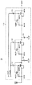
図5は、この発明の実施の形態1に従うセンスアンプの変更例の構成を示す図である。図5において、センスアンプは、内部ノードND1と内部ノードREFNの間に接続されかつそのゲートが内部ノードREFNに接続されるPチャネルMOSトランジスタPQ10と、内部ノードND1およびND10の間に接続されかつそのゲートが内部ノードREFNに接続されるPチャネルMOSトランジスタPQ11と、内部ノードND1と内部ノードND11の間に接続されかつそのゲートが内部ノードCELNに接続されるPチャネルMOSトランジスタPQ12と、内部ノードND1と内部ノードCELNの間に接続されかつそのゲートが内部ノードCELNに接続されるPチャネルMOSトランジスタPQ13と、相補イコライズ指示信号EQおよび♯EQに従って、内部ノードND10およびND11を電気的に短絡するCMOSトランスミッションゲートTX10と、内部ノードと接地ノードの間に接続されかつそのゲートが内部ノードND10に接続されるNチャネルMOSトランジスタNQ10と、内部ノードND11と接地ノードの間に接続されかつそのゲートが内部ノードND10に接続されるNチャネルMOSトランジスタNQ11を含む。
[Example of change]
FIG. 5 shows a structure of a modification of the sense amplifier according to the first embodiment of the present invention. In FIG. 5, the sense amplifier is connected between internal node ND1 and internal node REFN and connected between internal nodes ND1 and ND10, and P channel MOS transistor PQ10 whose gate is connected to internal node REFN. P channel MOS transistor PQ11 having its gate connected to internal node REFN, P channel MOS transistor PQ12 having its gate connected to internal node CELN and connected between internal node ND1 and internal node ND11, and internal node ND1 Internally connecting internal nodes ND10 and ND11 in accordance with P channel MOS transistor PQ13 connected between internal nodes CELN and having its gate connected to internal node CELN, and complementary equalize instruction signals EQ and #EQ MOS transmission gate TX10, an N-channel MOS transistor NQ10 connected between the internal node and the ground node and having its gate connected to internal node ND10, and connected between internal node ND11 and the ground node and having its gate connected internally N channel MOS transistor NQ11 connected to node ND10 is included.
この図5に示すセンスアンプの他の構成は、図2に示すセンスアンプの構成と同じであり、対応する部分には同一参照番号を付し、その詳細説明は省略する。 The other configuration of the sense amplifier shown in FIG. 5 is the same as the configuration of the sense amplifier shown in FIG. 2. Corresponding portions are denoted by the same reference numerals, and detailed description thereof is omitted.
PチャネルMOSトランジスタPQ4、PQ5およびPQ10−PQ13は、すべて埋込チャネル方式のPチャネルMOSトランジスタで構成される。PチャネルMOSトランジスタPQ10およびPQ11がカレントミラー段を構成し、またNチャネルMOSトランジスタNQ10およびNQ11がカレントミラー段を構成し、またさらに、PチャネルMOSトランジスタPQ12およびPQ13が、カレントミラー段を構成する。 P channel MOS transistors PQ4, PQ5 and PQ10-PQ13 are all formed of buried channel type P channel MOS transistors. P channel MOS transistors PQ10 and PQ11 form a current mirror stage, N channel MOS transistors NQ10 and NQ11 form a current mirror stage, and P channel MOS transistors PQ12 and PQ13 form a current mirror stage.
図5に示すセンスアンプの動作は、図3に示すタイミング図により示される。内部ノードREFNおよびCELNを同一電位に維持した状態で、参照電流Irefおよびセル電流Icelをセンス動作時流す。MOSトランジスタPQ10およびPQ11により参照電流Irefと同じ大きさの電流がノードND10に供給され、また、MOSトランジスタNQ10およびNQ11により、同じ大きさの電流が、ノードND10およびND11により駆動される。 The operation of the sense amplifier shown in FIG. 5 is shown by the timing chart shown in FIG. In a state where internal nodes REFN and CELN are maintained at the same potential, reference current Iref and cell current Icel are supplied during the sensing operation. MOS transistors PQ10 and PQ11 supply current of the same magnitude as reference current Iref to node ND10, and MOS transistors NQ10 and NQ11 drive the same magnitude of current by nodes ND10 and ND11.
MOSトランジスタPQ12およびPQ13が、カレントミラー段を構成し、セル電流Icelと同じ大きさの電流を、内部ノードND11へ供給する。したがって、イコライズ完了後のセンス動作時、内部ノードND10およびND11には、これらの参照電流Irefおよびセル電流Icelの大きさに応じた電位差が生じる。したがって、内部ノードND11またはND10の電位を内部読出データとして出力することにより、高速で、メモリセルデータを読出すことができる。 MOS transistors PQ12 and PQ13 form a current mirror stage, and supply a current having the same magnitude as cell current Icel to internal node ND11. Therefore, during the sensing operation after completion of equalization, potential differences corresponding to the magnitudes of reference current Iref and cell current Icel are generated in internal nodes ND10 and ND11. Therefore, memory cell data can be read at high speed by outputting the potential of internal node ND11 or ND10 as internal read data.
この図5に示すセンスアンプの構成の場合、内部ノードND10およびND11に、参照電流Irefおよびセル電流Icelの電位差が生じる。したがって、メモリセルデータ読出時、内部ノードREFNおよびCELNの容量の影響を抑制することができ、高速で、かつ高精度でメモリセルデータを読出すことができる。 In the configuration of the sense amplifier shown in FIG. 5, a potential difference between reference current Iref and cell current Icel occurs at internal nodes ND10 and ND11. Therefore, when memory cell data is read, the influence of the capacitances of internal nodes REFN and CELN can be suppressed, and memory cell data can be read at high speed and with high accuracy.
この図5に示すセンスアンプにおいても、昇圧電源ノードND1に内部電源電圧VCCよりも高い昇圧電圧Vbsを供給することにより、カレントミラー段を構成するMOSトランジスタPQ10−PQ13およびNQ10,NQ11を、飽和領域で動作させることができ、高速で、カレントミラー動作により、メモリセルデータの電流センスを行なって内部読出データを生成することができる。 In the sense amplifier shown in FIG. 5 as well, by supplying boosted voltage Vbs higher than internal power supply voltage VCC to boosted power supply node ND1, MOS transistors PQ10-PQ13 and NQ10, NQ11 constituting the current mirror stage are set in the saturation region. The memory cell data can be sensed by current mirror operation at a high speed and the internal read data can be generated.
以上のように、この発明の実施の形態1に従えば、メモリセルデータを読出すセンスアンプの電源電圧に、内部電源電圧よりも高い昇圧電圧を用いており、カレントミラー段を構成するトランジスタを飽和領域で低電源電圧下においても確実に動作させることができ、高精度でセンス動作を行なうことができる。 As described above, according to the first embodiment of the present invention, the boosted voltage higher than the internal power supply voltage is used as the power supply voltage of the sense amplifier for reading the memory cell data, and the transistors constituting the current mirror stage are used. The operation can be ensured even under a low power supply voltage in the saturation region, and the sensing operation can be performed with high accuracy.
また、参照ビット線およびビット線のプリチャージは、内部電源電圧を利用しており、昇圧電圧は、センス動作のみに利用しており、この昇圧電圧生成のための消費電力を低減することができる。 Further, the precharge of the reference bit line and the bit line uses the internal power supply voltage, and the boosted voltage is used only for the sensing operation, so that power consumption for generating the boosted voltage can be reduced. .
[実施の形態2]
図6は、実施の形態1におけるセンスアンプに供給される昇圧電圧Vbsを発生する部分の構成を概略的に示す図である。図6に示す昇圧電圧発生部は、図1に示す内部電圧発生回路6に含まれる。
[Embodiment 2]
FIG. 6 schematically shows a configuration of a portion that generates boosted voltage Vbs supplied to the sense amplifier in the first embodiment. The boosted voltage generating unit shown in FIG. 6 is included in internal
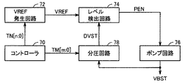
図6において、昇圧電圧発生部は、動作モード指示信号ACTと低電圧指示信号LVCを受けるAND回路10と、AND回路10の出力信号に応答して選択的に活性化され、活性化時、チャージポンプ動作により昇圧電圧を生成するポンプ回路11と、補の動作モード指示信号♯ACTと低電圧指示信号LVCを受けるAND回路12と、AND回路12の出力信号に従って活性化され、活性化時、チャージポンプ動作により、昇圧電圧を生成するスタンバイポンプ回路13と、動作モード指示信号ACTと補の低電圧指示信号♯LVCを受けるAND回路14と、AND回路14の出力信号の活性化時動作し、外部電源電圧を降圧して降圧電圧を生成する内部降圧回路(VDC回路)15と、補の動作モード指示信号♯ACTと補の低電圧指示信号♯LVCを受けるAND回路16と、AND回路16の出力信号に従って選択的に活性化され、活性化時、外部電源電圧を降圧するスタンバイVDC回路17と、低電圧指示信号LVCの活性化時導通し、ポンプ回路11およびスタンバイポンプ回路13の出力電圧をセンス昇圧電圧Vbsとして伝達するトランスファーゲート18と、補の低電圧指示信号♯LVCの非活性時導通し、VDC回路15およびスタンバイVDC回路17の生成電圧をセンス昇圧電圧Vbsとして伝達するトランスファーゲート19を含む。
In FIG. 6, the boosted voltage generator is selectively activated in response to an AND
図6においては、このトランスファーゲート18および19が、それぞれNチャネルMOSトランジスタで構成される場合を一例として示す。これらのトランスファーゲート18および19は、CMOSトランスミッションゲートで構成されてもよく、また、ボルテージフォロアで構成されても良い。
FIG. 6 shows an example in which each of
動作モード指示信号ACTは、この不揮発性半導体記憶装置がアクセスされるときに活性状態となり、動作サイクル期間中Hレベルに維持される。補の動作モード指示信号ACTは、この不揮発性半導体記憶装置がスタンバイ状態のときに活性化される。 Operation mode instruction signal ACT is activated when the nonvolatile semiconductor memory device is accessed, and is maintained at the H level during the operation cycle. Complementary operation mode instruction signal ACT is activated when the nonvolatile semiconductor memory device is in a standby state.
定電圧指示信号LVCは、外部電源電圧(VEX)が1.8Vであり、昇圧電圧Vbsが2.5Vのときに活性化される(Hレベルに設定される)。一方、外部電源電圧(VEX)が3.3Vであり、昇圧電圧Vbsが、2.5Vの場合に、補の低電圧指示信号♯LVCがHレベルに設定される。 Constant voltage instruction signal LVC is activated (set to H level) when external power supply voltage (VEX) is 1.8 V and boosted voltage Vbs is 2.5 V. On the other hand, when external power supply voltage (VEX) is 3.3 V and boosted voltage Vbs is 2.5 V, complementary low voltage instruction signal #LVC is set to the H level.
したがって、外部電源電圧が、たとえば1.8Vであり、昇圧電圧Vbsが、外部電源電圧よりも高い場合には、VDC回路15およびスタンバイVDC回路17は、常時非活性状態に維持される。一方、ポンプ回路11およびスタンバイポンプ回路13が、この不揮発性半導体記憶装置のアクティブサイクルおよびスタンバイサイクルにそれぞれ活性化され、昇圧動作を行なって昇圧電圧Vbsを生成する。トランスファーゲート18が導通状態に設定され、これらのポンプ回路11およびスタンバイポンプ回路13の出力電圧が昇圧電圧として伝達される。
Therefore, when external power supply voltage is 1.8 V, for example, and boosted voltage Vbs is higher than the external power supply voltage,
一方、外部電源電圧が、3.3Vであり、昇圧電圧Vbsよりも高い場合には、低電圧指示信号LVCがLレベルに設定され、補の低電圧指示信号♯LVCがHレベルに設定される。この状態においては、ポンプ回路11およびスタンバイポンプ回路13は、AND回路10および12の出力信号が常時Lレベルであるため、非活性状態に維持される。また、トランスファーゲート18も非導通状態に維持される。トランスファーゲート19が、導通状態となるため、AND回路14および16の出力信号に従って、VDC回路15およびスタンバイVDC回路17が、それぞれ、この不揮発性半導体記憶装置のアクティブサイクルおよびスタンバイサイクル時に活性化されて、降圧動作により、たとえば2.5Vの内部電圧を生成して、センス昇圧電圧Vbsを生成する。
On the other hand, when external power supply voltage is 3.3 V and higher than boosted voltage Vbs, low voltage instruction signal LVC is set to L level, and complementary low voltage instruction signal #LVC is set to H level. . In this state, pump
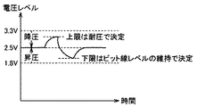
図7は、昇圧電圧Vbsの電圧変化許容範囲を概略的に示す図である。ポンプ回路11およびスタンバイポンプ回路13を用いて外部電源電圧を昇圧して昇圧電圧Vbsを生成する場合、ポンプ動作により、この昇圧電圧Vbsには、リップルが生じる。この場合、昇圧電圧Vbsの上限値は、この昇圧電圧Vbsを使用するMOSトランジスタの耐圧(デューティを考慮する)で決定される。一方、この昇圧電圧Vbsの下限値は、センス動作時にビット線を介してメモリセルのドレインに印加される読出電圧に要求される電圧レベルを必要期間維持する電圧レベルに設定される(この場合、昇圧電圧の下限電圧レベルは、バイアス電圧Vbiasの電圧レベルに応じて決定される)。これらの上下限値を満たすように、ポンプ回路11およびスタンバイポンプ回路13のポンプ数、レベル検知精度、応答速度およびデカップル容量値を設定する。
FIG. 7 is a diagram schematically showing the allowable voltage change range of the boosted voltage Vbs. When the external power supply voltage is boosted using the
図8は、ポンプ回路11の構成の一例を概略的に示す図である。図8において、ポンプ回路11は、並列に設けられるチャージポンプ20a−20nと、出力ノードNDAからの昇圧電圧Vbsの電圧レベルを検出するレベル検出回路21と、レベル検出回路21の出力信号に従って選択的に活性化され、活性化時、ポンプクロック信号PCKを生成するクロック発生回路22を含む。出力ノードNDAには、デカップル容量23が接続され、昇圧電圧Vbsを安定化する。
FIG. 8 is a diagram schematically showing an example of the configuration of the
レベル検出回路21およびクロック発生回路22へは、図6に示すAND回路10からのイネーブル信号ENPが与えられ、このイネーブル信号ENPの活性化時、レベル検出回路21およびクロック発生回路22が動作する。レベル検出回路21は、このイネーブル信号ENPの活性化時、昇圧電圧Vbsが所定電圧レベル以上のときに、クロック発生回路22のクロック発生動作を停止させ、所定電圧レベル以下となると、クロック発生回路22にポンプクロック信号PCKを発生させる。
The
クロック発生回路22は、たとえばリングオシレータで構成され、レベル検出回路21の出力信号とイネーブル信号ENPがともに活性状態のときに、所定の周期のポンプクロック信号PCKを生成する。
The
チャージポンプ20a−20nは、ポンプクロック信号PCKに従って容量素子を利用するチャージポンプ動作を行なって、出力ノードNDAへ電荷を供給して、昇圧電圧Vbsを生成する。 Charge pumps 20a-20n perform a charge pump operation using a capacitive element in accordance with pump clock signal PCK, supply charges to output node NDA, and generate boosted voltage Vbs.
このレベル検出回路21の検出精度、および応答速度と、デカップル容量23の容量値およびチャージポンプ20a−20nの数を、図7に示す昇圧電圧の上限値および下限値を満たすように設定する。
The detection accuracy and response speed of the
図9は、図6に示すVDC回路15の構成の一例を概略的に示す図である。図9において、VDC回路15は、出力ノードNDB上の電圧Vbsと基準電圧VRFとを比較する比較回路25と、比較回路25の出力信号に従って外部電源ノードから出力ノードNDBへ電流を供給する電流ドライブトランジスタ26と、出力ノードNDBの電圧を安定化するデカップル容量27を含む。
FIG. 9 schematically shows an example of the configuration of
比較回路25は、図6に示すAND回路14の出力信号(イネーブル信号)ENVに従って選択的に活性化される。比較回路25は、活性化時、出力ノードNDB上の電圧Vbsと基準電圧VRFとを比較し、電圧Vbsが基準電圧VRFよりも高いときには、電流ドライブトランジスタ26をオフ状態とする。一方、この電圧Vbsが基準電圧VRFよりも低いときには、比較回路25は、電流ドライブトランジスタ26のコンダクタンスを大きくして、外部電源ノードから出力ノードNDBへ電流を供給させて、電圧Vbsの電圧レベルを上昇させる。
The
この電流ドライブトランジスタ26および出力ノードNDBおよび比較回路25のフィードバックループの応答特性、比較回路25の比較精度およびデカップル容量27の容量値を適当な値に設定することにより、センス昇圧電源電圧Vbsのリップルを、図7示す上下限値の範囲内に設定することができる。
By setting the
図10は、低電圧指示信号LVCおよび♯LVCを発生する部分の構成の一例を示す図である。図10においては、ヒューズプログラム回路30により、低電圧指示信号LVCおよび♯LVCが生成される。このヒューズプログラム回路30は、溶断可能なリンク素子(ヒューズ素子)を含み、このリンク素子を選択的に溶断することにより、これらの低電圧指示信号LVCおよび♯LVCの一方をLレベル、他方をHレベルに設定する。
FIG. 10 shows an example of a configuration of a portion for generating low voltage instruction signals LVC and #LVC. In FIG. 10, low voltage instruction signals LVC and #LVC are generated by
この図10に示すヒューズプログラム回路30の構成に代えて、特定のボンディングパッドの電圧レベルをボンディングワイアなどにより設定して、低電圧指示信号LVCおよび♯LVCが生成されてもよい。また、これに代えて、マスク配線を用いて、マスタスライス工程のスライス工程においてこれらの信号LVCおよび♯LVCの電圧レベルが設定されてもよい。
Instead of the configuration of
なお、スタンバイポンプ回路13およびスタンバイVDC回路17も、それぞれ、ポンプ回路11およびVDC回路15と同様の構成を有し、スタンバイ時の電圧Vdsのリーク電流などに起因する電圧レベルの低下を補償することが要求されるだけである。したがって、これらのスタンバイポンプ回路13およびスタンバイVDC回路17は、電荷供給力は小さく、応じて、生成されるリップルも小さく、応答速度およびレベル検出精度は、アクティブサイクル時に動作するポンプ回路11およびVDC回路ほど、厳格には要求されない。
Note that the
以上のように、この発明の実施の形態2に従えば、センス昇圧電源電圧を、ポンプ回路またはVDC回路を用いて生成しており、外部電源電圧レベルに応じて、センス昇圧電源電圧を生成する回路を切り替えることにより、最適レベルのセンス昇圧電源電圧を生成することができる。 As described above, according to the second embodiment of the present invention, the sense boost power supply voltage is generated using the pump circuit or the VDC circuit, and the sense boost power supply voltage is generated according to the external power supply voltage level. By switching the circuits, it is possible to generate the sense boost power supply voltage at the optimum level.
また、外部電源電圧の電圧レベルが異なる用途に対しても、同一の回路構成で対応することができ、設計効率が改善される。 In addition, applications having different external power supply voltage levels can be handled with the same circuit configuration, and the design efficiency is improved.
[実施の形態3]
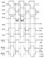
図11は、この発明の実施の形態3に従う不揮発性半導体記憶装置のデータ読出部の構成を概略的に示す図である。図11において、センスアンプ40は、図2または図5に示す構成を一例として有する。このセンスアンプ40に接続される内部読出データ線CELBDおよびおよび参照データ線REFBDには、それぞれ容量CBDおよびCRBDが接続される。
[Embodiment 3]
FIG. 11 schematically shows a structure of the data read portion of the nonvolatile semiconductor memory device according to the third embodiment of the present invention. 11, the
内部読出データ線(以下、セルセンスノードと称す)CELBDが、列選択ゲート回路42を介してメモリセルアレイ43のメインビット線MBL0−MBLnに接続される。この列選択ゲート回路42においては、Y選択信号y0−Ynをそれぞれゲートに受けるY選択ゲートYG0−YGnが、メインビット線MBL0−MBLnそれぞれに対応して設けられる。メインビット線MBL0−MBLnは、それぞれ、図示しないブロック選択ゲートを介してビット線BL0−BLnに接続される。図11においては、このブロック選択ゲートは図面を簡略するために示していない。
Internal read data lines (hereinafter referred to as cell sense nodes) CELBD are connected to main bit lines MBL 0 -MBLn of
ビット線BL0−BLnには、メモリセルNMC0−NMCnがそれぞれ接続される。1行に整列して配置されるメモリセルNMC0−NMCnに対してワード線WLが共通に設けられる。メインビット線MBL0−MBLnそれぞれには、容量C0−Cnが存在する。この容量C0−Cnは、配線容量などの寄生容量であってもよく、また対向する電極およびこれらの対向する電極の間の絶縁膜を有する現実の容量素子で構成されてもよい。 Memory cells NMC0 to NMCn are connected to bit lines BL0 to BLn, respectively. A word line WL is provided in common to memory cells NMC0 to NMCn arranged in a row. Each of main bit lines MBL0-MBLn has capacitors C0-Cn. The capacitances C0 to Cn may be parasitic capacitances such as wiring capacitances, or may be configured by actual capacitive elements having opposing electrodes and an insulating film between these opposing electrodes.
センスアンプ40に接続される参照データ線(以下、参照センスノードと称す)REFBDには、参照セル選択ゲート回路44を介して参照セルアレイ45に結合される。この参照セルアレイ45は、ワード線WLに結合される参照セルRMC1−RMC3を含む。これらの参照セルRMC1−RMC3は、それぞれ、導通時、参照電流Iref1、Iref2、Iref3を駆動する。これらの参照電流Iref1、Iref2、Iref3は、互いに値が異なり、4値データ読出時において読出データに応じて、これらの参照セルRMC1−RMC3から選択的に1つを導通状態とすることにより、4値データの値を、2分割探索法に従って判定する。
A reference data line (hereinafter referred to as a reference sense node) REFBD connected to the
この参照セルアレイ45においても、メモリセルアレイ43と同様ブロック選択ゲートを介して参照セルが参照メインビット線MBR1−MBR3に結合される。これらの参照メインビット線MBR1−MBR3には、容量CR1−CR3がそれぞれ存在する。これらの容量CR1−CR3も、また、配線容量などの寄生容量であってもよく、また現実の容量素子であってもよい。
In this
これらの参照メインビット線MBR1−MBR3それぞれに対応して、セル選択ゲートYGR1−YGR3が設けられる。これらのセル選択ゲートYGR1−YGR3のゲートへは、セル選択信号YR1−YR3がそれぞれ与えられる。これらのセル選択ゲートYGR1−YGR3は、それぞれ、参照データ線(参照センスノード)REFBDに共通に結合される。 Cell select gates YGR1-YGR3 are provided corresponding to these reference main bit lines MBR1-MBR3, respectively. Cell selection signals YR1-YR3 are applied to the gates of cell selection gates YGR1-YGR3, respectively. Each of these cell selection gates YGR1-YGR3 is commonly coupled to a reference data line (reference sense node) REFBD.
メモリセルNMC0−NMCnは、それぞれ、4値データを格納する。この場合、参照セル選択信号YR1−YR3のうちの参照セル選択信号YR2が選択状態へ駆動され、まず中間値の参照電流Iref2を供給し、メモリセルの駆動電流Icelと比較される。この第1回目の比較結果に従って、セル選択信号YR1およびYR3の一方が選択状態へ駆動される。したがって、これらの参照セル選択信号YR1−YR3は、選択メモリセルの記憶情報に応じて、その選択シーケンスが決定される。 Memory cells NMC0 to NMCn each store quaternary data. In this case, the reference cell selection signal YR2 of the reference cell selection signals YR1 to YR3 is driven to the selected state, and first, an intermediate value reference current Iref2 is supplied and compared with the drive current Icel of the memory cell. According to the first comparison result, one of cell selection signals YR1 and YR3 is driven to a selected state. Therefore, the selection sequence of these reference cell selection signals YR1-YR3 is determined according to the storage information of the selected memory cell.
メモリセルのデータ読出時(センス時)においては、ワード線WLの電圧レベルは一定である。参照セルを切換え、参照電流を変更することにより、ワード線電圧を変更する場合に比べて高速で、センスアンプ40によるセンス動作を行なってメモリセルデータを読出す。
At the time of data reading from the memory cell (at the time of sensing), the voltage level of word line WL is constant. By switching the reference cell and changing the reference current, the sensing operation by the
この図11に示す構成において、センスノードCELBDおよびREFBDの付随する容量は、以下の関係を満たすように設定される。 In the configuration shown in FIG. 11, the capacitances accompanying sense nodes CELBD and REFBD are set to satisfy the following relationship.
CBD+Ci>CRBD+CRj:
i=0−n,j=1−3
すなわち、セルセンスノードCELBDに接続される容量の値が、参照センスノードREFBDの容量値よりも常に大きくされる。次に、図11に示す不揮発性半導体記憶装置の4値データ読出時の動作について説明する。
CBD + Ci> CRBD + CRj:
i = 0-n, j = 1-3
That is, the value of the capacitance connected to the cell sense node CELBD is always larger than the capacitance value of the reference sense node REFBD. Next, the operation at the time of four-value data reading of the nonvolatile semiconductor memory device shown in FIG. 11 will be described.
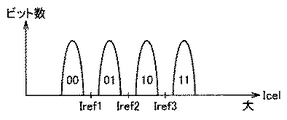
図12は、メモリセルNMC0−NMCnの電流分布を概略的に示す図である。これらのメモリセルNMC0−NMCnは、4値データ(00)、(01)、(10)、および(11)のいずれかを記憶しており、これらの4値データ(00)、(01)、(10)、および(11)の順に、メモリセルの駆動電流(セル電流)が大きくされる(しきい値電圧が小さくなる)。参照電流Iref1は、データ(00)および(01)に対応するセル電流の間の電流値であり、参照電流Iref2は、データ(01)および(10)に対応する電流の間の電流値である。参照電流Iref3は、データ(10)および(11)に対応する電流の間の電流値である。 FIG. 12 schematically shows a current distribution of memory cells NMC0 to NMCn. These memory cells NMC0 to NMCn store any one of quaternary data (00), (01), (10), and (11). These quaternary data (00), (01), In the order of (10) and (11), the drive current (cell current) of the memory cell is increased (threshold voltage is decreased). Reference current Iref1 is a current value between cell currents corresponding to data (00) and (01), and reference current Iref2 is a current value between currents corresponding to data (01) and (10). . The reference current Iref3 is a current value between currents corresponding to the data (10) and (11).
4値データ読出時においては、まず参照セルRMC2を選択し、参照電流Iref2を生成する。選択メモリセルの記憶データに応じて、この参照電流Iref2よりも大きなセル電流または小さなセル電流が駆動され、この大小判定により、上位ビットが“0”または“1”であると判定される。この判定結果に基づいて、参照電流が、参照電流Iref1またはIref3に設定される。これにより、下位ビットが“0”であるか“1”であるかが判定される。これらの2回のセンス動作により、4値データを読出すことができる。 At the time of reading quaternary data, reference cell RMC2 is first selected to generate reference current Iref2. A cell current larger or smaller than the reference current Iref2 is driven according to the data stored in the selected memory cell, and the upper bit is determined to be “0” or “1” based on the magnitude determination. Based on this determination result, the reference current is set to the reference current Iref1 or Iref3. Thereby, it is determined whether the lower bit is “0” or “1”. By these two sensing operations, quaternary data can be read.
図13は、この図11に示す不揮発性半導体記憶装置のデータ読出時の動作を示すタイミング図である。以下、図13を参照して、図11に示す不揮発性半導体記憶装置のデータ読出動作について説明する。 FIG. 13 is a timing chart showing an operation at the time of data reading of the nonvolatile semiconductor memory device shown in FIG. Hereinafter, the data read operation of the nonvolatile semiconductor memory device shown in FIG. 11 will be described with reference to FIG.
まず、ワード線WLが選択状態へ駆動され、その電圧レベルが所定の電圧レベルのHレベルとなる。 First, the word line WL is driven to a selected state, and its voltage level becomes an H level of a predetermined voltage level.
次いで、列選択ゲート回路42において、Y選択信号Yiがアドレス信号に従って選択状態へ駆動され、この選択列のメインビット線MBLiが、セルセンスノードCELBDに結合される。同様、また参照セル選択ゲート回路44において、参照セル選択信号YR2がHレベルとなり、参照セルRMC2に接続される参照メインビット線MBR2が、参照センスノードREFBDに結合される。
Next, in column
次いで、センスアンプ40が活性化され、先の実施の形態1において説明したように、センスアンプ40内からのプリチャージ電流に従ってセンスノードCELBDおよびおよびREFBDが所定の電圧レベルへ駆動される。これらのセンスノードCELBDおよびREFBDの電圧レベルが一定電圧レベルとなると、参照セルRMC2および選択メモリセルNMCi(図示せず)のドレイン電位が同じとなる。これにより、センスアンプ40において、この選択メモリセルNMCiと参照セルRMC2の駆動電流の差動増幅を行なうことができる。
Then,
参照セル選択信号YR2により、選択メモリセルNMCiの上位ビットの読出が完了すると、一旦、Y選択信号Yiおよび参照セル選択信号YR2が、Lレベルとなる。センスアンプ40が一旦非活性化され、センスノードCELBDおよびREFBDが接地電圧レベルにプリチャージされる。再び、Y選択信号Yiと参照セル選択信号YR1またはYR3が選択状態へ駆動される。参照セル選択信号YR1およびYR3のいずれが選択状態へ駆動されるかは、先の1回目のセンス動作により読出されたデータにより決定される。1回目のセンス動作と同様のセンス動作が、センスノードCELBDおよびREFBDが同一電圧レベルに収束した後に実行される。
When the reading of the upper bits of the selected memory cell NMCi is completed by the reference cell selection signal YR2, the Y selection signal Yi and the reference cell selection signal YR2 once become L level.
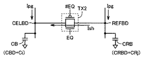
このセンス動作時において、センスノードCELBDおよびREFBDの容量値は不平衡である。センスアンプ40によるプリチャージ動作時においては、図14に示すように、センスノードREFBDとCELBDは、CMOSトランスミッションゲートTX2により電気的に短絡された状態にある。したがって、参照センスノードREFBDに対する容量CRB(=CRBD+CRj)が、セルセンスノードCELBDの容量(=CBD+Ci)よりも小さいため、この参照センスノードREFBDの電位は、セルセンスノードCELBDの電位よりも早く上昇する。このときCMOSトランスミッションゲートTX2はオン状態であるため、参照センスノードREFBDからセルセンスノードCELBDへ電流Ishが流れ、プリチャージ電流Ipgに加えて、選択メモリセルが接続されるビット線へ供給される。これにより、セルセンスノードCELBDの電位上昇速度が増加され、高速で、これらのセンスノードCELBDおよびREFBDを所定電圧レベルに収束させることができ、応じて早いタイミングでセンス動作を行なうことができる。センスノードの容量値が非平衡状態であるため、2回目のセンス動作時においても、再び、高速で、これらのセンスノードCELBDおよびREFBDを所定の電圧レベルへ収束させることができ、同様に、2回目のセンス動作開始タイミングをも早くすることができ、応じてアクセス時間を短縮することができる。
During this sensing operation, the capacitance values of the sense nodes CELBD and REFBD are unbalanced. During the precharge operation by the
なお、このセンスアンプ40の参照センスノードREFBDに接続する容量の容量値を、選択メモリセルが接続されるセルセンスノードCLBDの容量値よりも小さくする構成としては、現実の容量素子が、それらの容量値が調整されて、これらのセンスノードREFBDおよびCELBDに接続されてもよく、また、この参照センスノードREFBDの配線の長さ/幅を小さくして、その寄生容量を小さくすることにより実現されてもよい。
Note that, as a configuration in which the capacitance value of the capacitor connected to the reference sense node REFBD of the
なお、上述の説明においては、メモリセルNMCが、4値データを格納している場合について説明している。しかしながら、このメモリセルが2値データ(“1”および“0”)を記憶するメモリセルの場合であっても、同様、1回のセンス動作が行なわれるだけであり、センス動作開始タイミングを早くすることができ、アクセス時間を短縮することができる。 In the above description, the case where the memory cell NMC stores quaternary data is described. However, even if this memory cell is a memory cell storing binary data (“1” and “0”), only one sensing operation is performed, and the sensing operation start timing is advanced. Access time can be shortened.
以上のように、この発明の実施の形態3に従えば、センスアンプの参照センスノードの容量を、このセンスアンプのセルセンスノードの容量よりも小さくしており、高速で、これらのセンスノードおよび参照センスノードの電位を所定電圧レベルに収束させることができ、アクセス時間を短縮することができる。 As described above, according to the third embodiment of the present invention, the capacity of the reference sense node of the sense amplifier is made smaller than the capacity of the cell sense node of the sense amplifier, and these sense nodes and The potential of the reference sense node can be converged to a predetermined voltage level, and the access time can be shortened.
[実施の形態4]
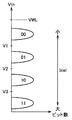
図15は、この発明の実施の形態4におけるメモリセルの記憶データのしきい値電圧の分布の一例を概略的に示す図である。図15においては、4値データを記憶するメモリセルのしきい値電圧の分布を示す。データ(11)を記憶するメモリセルのしきい値電圧は、電圧V3よりも低い。データ(10)を記憶するメモリセルのしきい値電圧は、電圧V2およびV3の間に分布する。データ(01)を記憶するメモリセルのしきい値電圧は、電圧V1およびV2の間に分布する。データ(00)を記憶するメモリセルのしきい値電圧は、電圧V1よりも高い電圧レベルであり、また、データ読出時にワード線に与えられるワード線読出電圧VWLよりも低い電圧レベルである。メモリセルのしきい値電圧が低いほど、ワード線読出電圧VWL印加時のメモリセル電流Icelが大きくなる。したがって、データ(11)を記憶するメモリセルの駆動電流が、データ(00)を記憶するメモリセルの駆動電流よりもデータ読出時大きくなる。
[Embodiment 4]
FIG. 15 schematically shows an example of threshold voltage distribution of data stored in a memory cell according to the fourth embodiment of the present invention. FIG. 15 shows the distribution of threshold voltages of memory cells storing quaternary data. The threshold voltage of the memory cell storing data (11) is lower than voltage V3. The threshold voltage of the memory cell storing data (10) is distributed between voltages V2 and V3. The threshold voltage of the memory cell storing data (01) is distributed between voltages V1 and V2. The threshold voltage of the memory cell storing data (00) is a voltage level higher than voltage V1, and a voltage level lower than word line read voltage VWL applied to the word line at the time of data reading. The lower the threshold voltage of the memory cell, the larger the memory cell current Icel when the word line read voltage VWL is applied. Therefore, the drive current of the memory cell storing data (11) is larger at the time of data reading than the drive current of the memory cell storing data (00).
消去動作時および書込動作時においては、このメモリセルの記憶データに応じて、そのしきい値電圧が設定される。今、しきい値電圧が最も低くされる状態を消去状態と呼ぶことにする。すなわち、データ(11)を記憶する状態が、消去状態である。この消去動作後、記憶データに応じて、順次、メモリセルのしきい値が高くされ、データの書込が行なわれる。この書込動作時および消去動作時においては、しきい値電圧の分布範囲の上限および下限内に、メモリセルのしきい値電圧が存在するかのベリファイ動作が行なわれる。 In the erase operation and the write operation, the threshold voltage is set according to the data stored in the memory cell. Now, the state where the threshold voltage is the lowest is called an erase state. That is, the state in which data (11) is stored is the erased state. After the erasing operation, the threshold value of the memory cell is sequentially increased according to the stored data, and data writing is performed. In the writing operation and the erasing operation, a verify operation is performed to determine whether the threshold voltage of the memory cell exists within the upper and lower limits of the threshold voltage distribution range.
ベリファイ動作時においては、ベリファイセンスアンプを用いてベリファイ参照電流を生成して各データに応じた上限電流および下限電流を設定して、メモリセル電流が、そのベリファイ参照電流の規定する領域内に存在するかの判定が行なわれる。このベリファイ動作時において、ワード線へは、従来、通常のデータ読出時(外部へのデータ読出)と同様のワード線読出電圧VWLが印加される。 During a verify operation, a verify reference current is generated using a verify sense amplifier, an upper limit current and a lower limit current are set according to each data, and a memory cell current exists in a region defined by the verify reference current. A determination is made as to whether to do so. In this verify operation, word line read voltage VWL similar to that in normal data read (data read to the outside) is conventionally applied to the word line.
4値データを書込んだ後のメモリセルの電流分布としては、図12に示される電流分布が得られる。このような電流分布に基づいてベリファイ動作を行なう場合、各セル電流領域の上限値および下限値のベリファイ電流が生成されて、メモリセルの駆動電流と比較される。ベリファイ時に用いられるベリファイセンスアンプは、通常のデータ読出用のセンスアンプと同一構成を有しており、ベリファイ動作およびデータ読出動作にセンスアンプが共用されてもよいが、以下では説明を簡単にするため、ベリファイセンスアンプと読出用のセンスアンプ(実施の形態1において詳細に説明したセンスアンプ)は、別々に設けられるとして説明する。 The current distribution shown in FIG. 12 is obtained as the current distribution of the memory cell after the quaternary data is written. When the verify operation is performed based on such a current distribution, an upper limit value and a lower limit value verify current of each cell current region are generated and compared with the drive current of the memory cell. The verify sense amplifier used at the time of verify has the same configuration as a normal data read sense amplifier, and the sense amplifier may be shared for the verify operation and the data read operation. However, the following description is simplified. Therefore, it is assumed that the verify sense amplifier and the read sense amplifier (the sense amplifier described in detail in the first embodiment) are provided separately.
このベリファイ動作時において、図16に示すように、電流分布領域の下端(データ00)の下部の領域のメモリセルに対するベリファイ動作時においては、ワード線電圧(メモリセルトランジスタのゲート電圧)を、通常のデータ読出時に与えられる電圧VWLよりも高い電圧レベルに設定してベリファイ動作を行なう。電流分布の下端のセルのベリファイ動作時、読出電圧VWL印加時におけるセル電流が、図17に示すように下側ベリファイ電流Iver0よりも低いメモリセルに対しては、ほぼオフ状態であり、駆動電流は極めて小さい。センスアンプにおいては、通常の読出時と同程度のセル電流が供給することにより、メモリセルデータを正確にセンスして正確なベリファイ動作を保証することができる。この場合、下限電流よりも小さなセル電流のメモリセルに対しては再度消去を行って、そのしきい値電圧を高くすることにより、正確に、駆動電流分布、すなわち、しきい値電圧分布を狭くすることができ、多値データ記憶時における各データ値に対応する駆動電流分布領域を狭くすることができ、多値データの各参照電流に対するマージンを大きくすることができる。 In this verify operation, as shown in FIG. 16, in the verify operation for the memory cell in the region below the lower end (data 00) of the current distribution region, the word line voltage (gate voltage of the memory cell transistor) is normally set. The verify operation is performed by setting the voltage level higher than the voltage VWL applied at the time of data reading. In the verify operation of the cell at the lower end of the current distribution, the memory current when the read voltage VWL is applied is lower than the lower verify current Iver0 as shown in FIG. Is extremely small. In the sense amplifier, by supplying a cell current of the same level as in normal reading, it is possible to accurately sense the memory cell data and ensure an accurate verify operation. In this case, the memory cell having a cell current smaller than the lower limit current is erased again and its threshold voltage is increased to accurately narrow the drive current distribution, that is, the threshold voltage distribution. In addition, the drive current distribution region corresponding to each data value at the time of storing multi-value data can be narrowed, and the margin for each reference current of multi-value data can be increased.
この電流分布のメモリセルのベリファイ時、すなわち下限電流のベリファイ時においては、通常のデータ読出時に印加される読出ワード線電圧VWLよりも高い電圧VWLHをベリファイ時に印加する。この場合、図17の破線で示す領域メモリセルの駆動電流が大きくなり、下側ベリファイ電流Iver0よりも高くなり、これらのメモリセルが、データ(00)を格納していることが検証される。また、正確に、データ(00)のメモリセルの分布領域の上限ベリファイ時においては、上限ベリファイ電流を供給して、データ(00)を記憶するメモリセルの駆動電流が、参照電流Iref1よりも下部にあることが識別される。このデータ(00)の記憶するメモリセルの電流分布の識別可能領域を、下限側において広くすることができ、正確な検証動作を行なうことができる。 At the time of verifying the memory cell having this current distribution, that is, at the time of verifying the lower limit current, a voltage VWLH higher than the read word line voltage VWL applied during normal data reading is applied during verification. In this case, the drive current of the area memory cell indicated by the broken line in FIG. 17 increases and becomes higher than the lower verify current Iver0, and it is verified that these memory cells store data (00). In addition, when the upper limit verify of the distribution region of the memory cell of data (00) is accurately performed, the upper limit verify current is supplied and the drive current of the memory cell storing the data (00) is lower than the reference current Iref1. Is identified. The identifiable region of the current distribution of the memory cell storing this data (00) can be widened on the lower limit side, and an accurate verification operation can be performed.
一方、この電流分布の上部のメモリセルの検証時においては、図16に示すように、読出ワード線電圧VWLよりも低いゲート電圧を印加する。この状態において、図18に示すように、通常の読出ワード線電圧VWL印加時の破線で示すメモリセルの駆動電流は、それよりも低いベリファイワード線電圧VWLL印加時には小さくなり、上限ベリファイ電流Iver1よりも小さい電流レベルに低下する。 On the other hand, at the time of verifying the memory cell above the current distribution, a gate voltage lower than the read word line voltage VWL is applied as shown in FIG. In this state, as shown in FIG. 18, the drive current of the memory cell indicated by the broken line when the normal read word line voltage VWL is applied becomes smaller when the lower verify word line voltage VWLL is applied, and is higher than the upper limit verify current Iver1. Also decreases to a lower current level.
電流分布上端のメモリセルにおいては、過剰に電流が流れ、配線抵抗などにおける電圧降下で、ビット線電圧レベルを維持することができなくなり、メモリセルのドレイン電圧が低下する。この結果、セル電流Icelが低減されるため、上側に広がるメモリセル電流分布を正確に得ることができない。また、このような電流分布上端のメモリセルが駆動する過剰電流は、センスアンプの電源に昇圧電圧を用いる場合消費電流が大きくなり、昇圧電圧発生部は、安定に昇圧電圧を生成することができなくなる可能性がある。メモリセル電流分布上端のベリファイ動作時においては、ワード線電圧を、読出ワード線電圧VWLよりも低い電圧VWLLに設定し、ベリファイ動作を行なうことにより、読出ワード線電圧VWLを印加したベリファイ動作時よりも、広範囲のメモリセル電流の分布を識別することができ、過剰セル電流を駆動するメモリセルを識別して、そのしきい値電圧を高くして、駆動電流を低減することができる。これにより、電流分布の上限の識別可能領域が広くなり、その識別結果に従ってしきい値電圧の調整を行うことにより、しきい値電圧分布すなわちしきい値電圧分布を狭くすることができ、センスアンプに対するセル電流の分布を小さくすることができ、正確なセンス動作を保証することができる。 In the memory cell at the upper end of the current distribution, an excessive current flows, and the bit line voltage level cannot be maintained due to a voltage drop in the wiring resistance or the like, and the drain voltage of the memory cell is lowered. As a result, since the cell current Icel is reduced, the memory cell current distribution spreading upward can not be obtained accurately. Further, the excessive current driven by the memory cell at the upper end of the current distribution consumes a large amount of current when the boosted voltage is used for the power supply of the sense amplifier, and the boosted voltage generator can stably generate the boosted voltage. There is a possibility of disappearing. In the verify operation at the upper end of the memory cell current distribution, the word line voltage is set to a voltage VWLL lower than the read word line voltage VWL, and the verify operation is performed, thereby performing the verify operation when the read word line voltage VWL is applied. However, it is possible to identify a wide range of memory cell current distribution, identify a memory cell that drives an excessive cell current, increase its threshold voltage, and reduce the drive current. As a result, the identifiable area at the upper limit of the current distribution is widened, and the threshold voltage distribution, that is, the threshold voltage distribution can be narrowed by adjusting the threshold voltage according to the identification result. Cell current distribution can be reduced, and an accurate sensing operation can be ensured.
したがって、この書込/消去時のベリファイ動作時に、読出ワード線電圧VWLを用いてベリファイ動作を行なう構成に代えて、そのベリファイ対象のメモリセルの電流分布の位置に応じてワード線電圧を変更することにより、メモリセル電流分布の上限および下限の識別の範囲を広くすることができ、書込/消去のベリファイを正確に行なうことができ、書込/消去時間を短縮することができる。 Therefore, the word line voltage is changed according to the position of the current distribution of the memory cell to be verified, instead of the configuration in which the verify operation is performed using read word line voltage VWL during the verify operation at the time of writing / erasing. As a result, the range of identification of the upper limit and the lower limit of the memory cell current distribution can be widened, the verify of write / erase can be performed accurately, and the write / erase time can be shortened.
また、中央の参照電流Iref1、Iref2およびIref3の近傍の電流分布でのベリファイ動作時においては、ベリファイ時のワード線電圧を読出ワード線電圧VWLと同じ電圧レベルに設定する。これにより、データ読出時とベリファイ動作時のワード線電圧が同じであり、ベリファイ時および通常動作時において高精度のセンス動作を行なうことができる。 In a verify operation with a current distribution in the vicinity of the central reference currents Iref1, Iref2, and Iref3, the word line voltage at the time of verify is set to the same voltage level as the read word line voltage VWL. Thereby, the word line voltage at the time of data reading and at the time of verifying operation is the same, and a highly accurate sensing operation can be performed at the time of verifying and during normal operation.
なお、図18において、メモリセル電流分布の上限領域のメモリセルのベリファイ動作時において、単に、ワード線に印加される電圧を、電圧VWLLに設定し、このときのセル電流が、参照電流Iref3よりも高い電流であるかを判定するベリファイ動作が行なわれてもよい。たとえば、データ(11)の記憶するメモリセルにおいて、ワード線に6V印加時、下限領域が60μAの電流を駆動し、上限のメモリセルが100μAを駆動する状態を考える。この場合、ワード線電圧を4Vに設定し、上限領域のメモリセルの駆動電流を、60μAに設定する。センスアンプにおいて、データ(11)の上限領域および下限領域いずれにおいてもメモリセル電流がともに60μAであり、ベリファイ電流として、参照電流Iref3と同じ大きさの電流を利用することにより、正確なベリファイ動作を行なうことができる。ただし、この場合、参照セルにおいては、同様、ワード線電圧が低下しており、その駆動電流が小さくされているため、参照セルの駆動する参照電流を利用して、上限領域のベリファイ動作を行なうことはできない(参照電流を駆動する電流が、参照電流Iref3よりも小さくなっているため)。この場合、ベリファイ電流を、ベリファイ参照セルまたは定電流回路を利用して別途生成してベリファイ動作を行う。 In FIG. 18, during the verify operation of the memory cell in the upper limit region of the memory cell current distribution, the voltage applied to the word line is simply set to the voltage VWLL, and the cell current at this time is greater than the reference current Iref3. A verify operation for determining whether the current is too high may be performed. For example, in the memory cell storing data (11), when 6V is applied to the word line, consider a state where the lower limit region drives a current of 60 μA and the upper limit memory cell drives 100 μA. In this case, the word line voltage is set to 4 V, and the drive current of the memory cell in the upper limit region is set to 60 μA. In the sense amplifier, the memory cell current is 60 μA in both the upper limit region and the lower limit region of the data (11), and an accurate verify operation is performed by using a current having the same magnitude as the reference current Iref3 as the verify current. Can be done. However, in this case, in the reference cell, similarly, the word line voltage is lowered and the drive current is reduced. Therefore, the verify operation of the upper limit region is performed using the reference current driven by the reference cell. (The current that drives the reference current is smaller than the reference current Iref3). In this case, a verify current is separately generated using a verify reference cell or a constant current circuit to perform a verify operation.
また、データ(00)の電流分布の下限領域についても、ベリファイワード線電圧を高くしてベリファイ電流として参照電流Iref1が用いられても良い。この場合においても、参照電流は、ベリファイ電流発生回路を利用して生成する。 For the lower limit region of the current distribution of data (00), the reference current Iref1 may be used as the verify current by increasing the verify word line voltage. Even in this case, the reference current is generated using the verify current generating circuit.
図19は、この発明の実施の形態4に従う半導体記憶装置のベリファイ動作を示すフロー図である。以下、図19を参照して、この発明の実施の形態4に従うベリファイ動作について説明する。なお、以下の説明においては、メモリセルのしきい値電圧の低い状態から順次しきい値電圧を高い状態へ設定する書込シーケンスを一例として示す。 FIG. 19 is a flowchart showing a verify operation of the semiconductor memory device according to the fourth embodiment of the present invention. Hereinafter, a verify operation according to the fourth embodiment of the present invention will be described with reference to FIG. In the following description, a write sequence for sequentially setting the threshold voltage from a low state to a high state is shown as an example.
ベリファイ動作時において、まずメモリセルがすべてしきい値電圧が低い状態に設定され、分布上限(電流分布の上限値)に対するベリファイ動作が行なわれるかの判定が行なわれる(ステップST1)。この電流分布の上限のセルに対するベリファイ動作が行なわれる場合、ワード線電圧を電圧VWLLに設定し、また、参照電流としてベリファイ電流Iver1を設定し、ベリファイ動作を実行する(ステップST2)。 During the verify operation, all memory cells are first set to a state in which the threshold voltage is low, and it is determined whether or not the verify operation for the distribution upper limit (current distribution upper limit value) is performed (step ST1). When the verify operation is performed on the upper limit cell of the current distribution, the word line voltage is set to the voltage VWLL, the verify current Iver1 is set as the reference current, and the verify operation is executed (step ST2).
一方、ステップST1において分布上限以外のセルに対するベリファイであると判定されると、次いで、セル電流分布の下限値、すなわちしきい値電圧の最も大きい状態に対するベリファイ動作が行なわれるかの判定が実行される(ステップST3)。電流分布の下限領域のメモリセルに対するベリファイ動作である場合には、ワード線電圧が、電圧VWLHに設定され、また、参照電流としてベリファイ電流Iver0が設定され、ベリファイ動作が実行される(ステップST4)。 On the other hand, if it is determined in step ST1 that the verification is for a cell other than the upper limit of the distribution, then it is determined whether the verify operation is performed for the lower limit value of the cell current distribution, that is, the state where the threshold voltage is the highest. (Step ST3). When the verify operation is performed on the memory cells in the lower limit region of the current distribution, the word line voltage is set to the voltage VWLH, the verify current Iver0 is set as the reference current, and the verify operation is executed (step ST4). .
電流分布の上限領域および下限領域いずれでもない場合には、対応の記憶データの領域の電流分布の上限または下限に応じてベリファイ電流が設定される。このとき、ワード線には、読出ワード線電圧VWLに設定され、ベリファイ動作が実行される(ステップST5)。 If neither the upper limit area nor the lower limit area of the current distribution is set, the verify current is set according to the upper limit or lower limit of the current distribution in the corresponding storage data area. At this time, the read word line voltage VWL is set to the word line, and the verify operation is executed (step ST5).
ステップST2、ST4およびST5におけるベリファイ動作により、正確に対応のメモリセルがベリファイ電流条件(ベリファイ電流以下または以上)を満たしているかの判定が行なわれる(ステップST6)。このベリファイ判定動作時において、所定の条件が満たされていると判定された場合には、各ベリファイ動作シーケンスに応じて次の処理が実行される(ステップST7)。一方、ベリファイ動作時において、この不良セル、すなわちベリファイ条件を満たさないメモリセルが存在する場合には、再び、その不良セルのしきい値電圧を調整することが再び行なわれる(ステップST8)。この再試行のステップ(ST8)が実行された後、再び、ステップST1に戻り、ベリファイ動作が実行される。 By the verify operation in steps ST2, ST4, and ST5, it is determined whether the corresponding memory cell accurately satisfies the verify current condition (below verify current or above) (step ST6). In the verify determination operation, when it is determined that a predetermined condition is satisfied, the following processing is executed according to each verify operation sequence (step ST7). On the other hand, if there is a defective cell, that is, a memory cell that does not satisfy the verification condition, the threshold voltage of the defective cell is adjusted again (step ST8). After this retry step (ST8) is executed, the process returns to step ST1 again and the verify operation is executed.
ベリファイ動作は、メモリセルの記憶データに応じて消去を含む各データ書込後、各データについて実行される。 The verify operation is executed for each data after each data write including erasure according to the data stored in the memory cell.
メモリセルデータの書込/消去が実行されるとき、予め定められたベリファイシーケンスに従ってベリファイ動作が実行される。このベリファイ動作時、図1に示す制御回路5の制御の下に、内部電圧発生回路6からのワード線電圧Vwの電圧レベルを調整し、またベリファイ電流が、ベリファイ対象のデータに応じた電流レベルに設定されて、図1に示す読出回路4に含まれるベリファイセンスアンプに供給される。この場合、読出回路4内のセンスアンプが、ベリファイ動作およびデータ読出動作両者において共通に用いられる場合には、参照セルからの参照電流に代えて、ベリファイ電流がセンスアンプへ供給される。
When writing / erasing of memory cell data is executed, a verify operation is executed according to a predetermined verify sequence. During this verify operation, the voltage level of the word line voltage Vw from the internal
以上のように、この発明の実施の形態4に従えば、メモリセルの電流分布の上限および下限に対し、ベリファイ時のワード線電圧を調整しており、下限領域のメモリセルおよび上限領域のメモリセルの識別可能領域を広くすることができ、正確なベリファイ動作を行なうことができる。 As described above, according to the fourth embodiment of the present invention, the word line voltage at the time of verification is adjusted with respect to the upper limit and lower limit of the current distribution of the memory cell, and the memory cell in the lower limit region and the memory in the upper limit region The identifiable area of the cell can be widened, and an accurate verify operation can be performed.
また、電流分布の上限および下限領域の間の領域のメモリセルに対しては、データ読出と同じ電圧レベルのベリファイ電圧が供給されており、ベリファイ動作時およびデータ読出動作モード時において同じマージンでセンス動作を行なうことができ、データ読出時および書込/消去ベリファイ時におけるセンス動作を高精度に一致させることができ、高精度のセンス動作を実現することができる。 The verify voltage at the same voltage level as that of data read is supplied to the memory cells in the region between the upper and lower limit regions of the current distribution, and sensing is performed with the same margin during the verify operation and the data read operation mode. The operation can be performed, the sensing operation at the time of data reading and writing / erasing verification can be made to coincide with each other with high accuracy, and a highly accurate sensing operation can be realized.
[実施の形態5]
図20は、この発明の実施の形態5に従う不揮発性半導体記憶装置のセンスアンプに関連する部分の構成を示す図である。図20において、センスアンプ40は、実施の形態1に示すセンスアンプと同様の構成を備え、センスノードCELBDおよびREFBDが、それぞれ、メモリセルNMCおよび参照セルRMCにセンス動作時結合される。この図20に示す構成においては、センスアンプ40に対して、定電圧VRSAを生成する定電圧発生回路50と、選択信号SELNに従って定電圧VRSAを伝達するトランスファーゲートSQNと、センスノードCELBDに結合され、定電圧VRSAを転送ゲートSQNを介してゲートに受けて、センスノードCELBDから定電流を接地ノードへ放電するNチャネルMOSトランジスタQNと、選択信号SELRに従って、定電圧VRSAを伝達する転送ゲートSQRと、転送ゲートSQRを介してゲートに定電圧VRSAを受け、参照センスノードREFBDから定電流を接地ノードへ放電するNチャネルMOSトランジスタQRがさらに設けられる。
[Embodiment 5]
FIG. 20 shows a structure of a portion related to the sense amplifier of the nonvolatile semiconductor memory device according to the fifth embodiment of the present invention. 20,
定電圧発生回路50は、内部電源ノードとノードND30の間に接続されかつそのゲートがノードND30に接続されるPチャネルMOSトランジスタPQ30と、内部ノードND30と接地ノードの間に接続されかつそのゲートがノードND30に接続されるNチャネルMOSトランジスタNQ30と、電源ノードと内部ノードND31の間に接続されかつそのゲートが内部ノードND30に接続されるPチャネルMOSトランジスタPQ31と、ノードND31と接地ノードの間に接続されかつそのゲートがノードND31に接続されるNチャネルMOSトランジスタNQ31を含む。
Constant
MOSトランジスタNQ31、QNおよびQRは、サイズ(チャネル幅とチャネル長の比)が同じである。PチャネルMOSトランジスタPQ30およびPQ31はカレントミラー段を構成し、MOSトランジスタPQ31は、MOSトランジスタPQ30を流れる電流のミラー電流を内部電源ノードから供給する。ノードND30へMOSトランジスタPQ30から供給される電流により電圧がMOSトランジスタにより生成され、これらのMOSトランジスタPQ30およびNQ30の駆動電流が等しくなるようにノードND30の電圧レベルが設定され、応じて、一定の電流がこれらのMOSトランジスタPQ30およびNQ30に流れる。この一定電流のミラー電流がMOSトランジスタPQ31を介して流れる。MOSトランジスタNQ31が、電流/電圧変換素子として機能し、このMOSトランジスタPQ31から供給される電流を電圧に変換して、定電圧VRSAを生成する。 MOS transistors NQ31, QN and QR have the same size (ratio of channel width to channel length). P channel MOS transistors PQ30 and PQ31 constitute a current mirror stage, and MOS transistor PQ31 supplies a mirror current of the current flowing through MOS transistor PQ30 from the internal power supply node. A voltage is generated by the MOS transistor by the current supplied from the MOS transistor PQ30 to the node ND30, and the voltage level of the node ND30 is set so that the drive currents of these MOS transistors PQ30 and NQ30 are equal. Flows through these MOS transistors PQ30 and NQ30. This constant mirror current flows through the MOS transistor PQ31. The MOS transistor NQ31 functions as a current / voltage conversion element, converts the current supplied from the MOS transistor PQ31 into a voltage, and generates a constant voltage VRSA.
選択信号SELNおよびSELRは、この定電圧VRSAに比べて十分高い電圧レベルであり、転送ゲートSQNおよびSQRは、導通時、この定電圧VRSAを、閾値電圧損失を伴うことなく、それぞれ、MOSトランジスタQNおよびQRのゲートに伝達する。転送ゲートSQNの導通時、MOSトランジスタNQ31およびQNがカレントミラー回路を構成し、MOSトランジスタQNには、MOSトランジスタNQ31を流れる電流と同じ大きさの電流が流れる(サイズが同じ場合)。同様、転送ゲートSQRの導通時、MOSトランジスタNQ31およびQRがカレントミラー回路を構成し、MOSトランジスタQRが、このMOSトランジスタNQ31が駆動する電流と同じ大きさの電流を駆動する(サイズが同じ場合)。 The selection signals SELN and SELR are at a sufficiently high voltage level as compared with the constant voltage VRSA. When the transfer gates SQN and SQR are turned on, the constant voltage VRSA is transmitted to the MOS transistor QN without any threshold voltage loss. And to the QR gate. When transfer gate SQN is turned on, MOS transistors NQ31 and QN form a current mirror circuit, and a current having the same magnitude as that flowing through MOS transistor NQ31 flows through MOS transistor QN (when the size is the same). Similarly, when transfer gate SQR is conductive, MOS transistors NQ31 and QR form a current mirror circuit, and MOS transistor QR drives a current having the same magnitude as that driven by MOS transistor NQ31 (when the sizes are the same). .
この定電圧発生回路50において、MOSトランジスタPQ30のサイズ(チャネル幅)を変更可能にすることにより、この定電圧VRSAの電圧レベルを変更することができ、MOSトランジスタQNおよびQRが駆動する電流量を、所望の値に設定することができる。 次に、図20に示す回路の動作について説明する。
In this constant
(i) SELN=Lレベル、かつSELR=Hレベル:
この状態においては、転送ゲートSQNがオフ状態、転送ゲートSQRがオン状態であり、参照セルRMCに対して設けられるトランジスタQRが定電流源として動作する。この状態において、参照セルRMCを選択しない状態で、メモリセルNMCを選択してセンスアンプ40でセンス動作を行なう。この場合、参照セルRMCが規定する参照電流値と異なる電流値でセンス動作を行なうことができる。したがって、この状態で、定電圧発生回路50のMOSトランジスタPQ30のサイズを変更して、定電圧VRSAを変更することにより、MOSトランジスタQRの駆動電流を変更することができ、メモリセルNMCを流れる電流値を詳細に解析することができる。
(I) SELN = L level and SELR = H level:
In this state, transfer gate SQN is off and transfer gate SQR is on, and transistor QR provided for reference cell RMC operates as a constant current source. In this state, in a state where the reference cell RMC is not selected, the memory cell NMC is selected and the
(ii) SELN=HレベルかつSELR=Lレベル:
この状態においては、転送ゲートSQNがオン状態、転送ゲートSQRがオフ状態であり、MOSトランジスタQNが、定電圧VRSAに従って、定電流をセルセンスノードCELBDから駆動する。この状態においては、メモリセルNMCの選択は行なわず、参照セルRMCを選択して、センスアンプ40でセンス動作を行なう。MOSトランジスタPQ30のサイズ(チャネル幅)を変更してその駆動電流を変更することにより、定電圧発生回路50からの定電圧VRSAを変更して、MOSトランジスタQNが駆動する電流を変更することができる。したがって、この場合、参照セルRMCを流れる電流値を詳細に解析することができる。参照電流を所望の値に設定したい場合、このセンス動作の結果を用いて、所望の参照電流が得られるように、参照セルのしきい値電圧を制御することができる。
(Ii) SELN = H level and SELR = L level:
In this state, transfer gate SQN is on and transfer gate SQR is off, and MOS transistor QN drives a constant current from cell sense node CELBD according to constant voltage VRSA. In this state, the memory cell NMC is not selected, the reference cell RMC is selected, and the
(iii) SELN=HレベルかつSELR=Hレベル:
この状態においては、転送ゲートSQNおよびSQRがともにオン状態であり、MOSトランジスタQNおよびQRがともに定電流を駆動する。この状態において、メモリセルNMCおよび参照セルRMCをともに選択することにより、センスアンプ40のセンスノードCELBDおよびREFBDを流れる電流にオフセットを持たせることができる。
(Iii) SELN = H level and SELR = H level:
In this state, transfer gates SQN and SQR are both on, and MOS transistors QN and QR both drive a constant current. In this state, by selecting both the memory cell NMC and the reference cell RMC, the current flowing through the sense nodes CELBD and REFBD of the
一般的な差動増幅器においては、電流値に対して感度が一定でなく、いわゆるヒット範囲と呼ばれる感度の高い電流範囲と比較的感度の低い電流範囲とが存在する。このMOSトランジスタQNおよびQRをともにオン状態に設定することにより、センスアンプ40のカレントミラー段を流れる電流にオフセットを持たせることにより、感度の高い電流範囲に移行させてセンス動作を行なわせることができ、高精度な電流差動増幅を実現することができる。
In a general differential amplifier, the sensitivity is not constant with respect to the current value, and there is a current range with high sensitivity called a hit range and a current range with relatively low sensitivity. By setting both MOS transistors QN and QR to the on state, the current flowing through the current mirror stage of the
したがって、センスアンプ40のセンスノードCELBDおよびREFBDに、選択的に活性化されかつ互いに独立に活性化される定電流源を接続して、定電流を駆動することにより、メモリセルおよび参照セルを流れる電流を詳細に解析することができ、また、センスアンプ40のセンスノードに対してオフセット電流を流すことができ、センス感度の高い領域でセンス動作を行なうことができ、高精度のセンス動作を行なうことができる。
Therefore, a constant current source that is selectively activated and activated independently of each other is connected to sense nodes CELBD and REFBD of
なお、この図20に示す構成において、転送ゲートSQNおよびSQRがオフ状態のときには、MOSトランジスタQNおよびQRのゲートがフローティング状態となる。この場合、転送ゲートSQNおよびSQRと相補的に導通するNチャネルMOSトランジスタを用いて、これらのMOSトランジスタQNおよびQRのゲートを接地ノードに結合する。これにより、MOSトランジスタQNおよびQRのゲートが、フローティング状態になるのを防止することができる。 In the configuration shown in FIG. 20, when transfer gates SQN and SQR are off, the gates of MOS transistors QN and QR are in a floating state. In this case, N channel MOS transistors that are complementarily connected to transfer gates SQN and SQR are used to couple the gates of these MOS transistors QN and QR to the ground node. Thereby, the gates of MOS transistors QN and QR can be prevented from entering a floating state.
また、転送ゲートSQNおよびSQRに代えて、CMOSトランスミッションゲートが用いられてもよい。 Further, a CMOS transmission gate may be used instead of the transfer gates SQN and SQR.
図21は、図20に示す定電圧発生回路50のMOSトランジスタPQ30のサイズ変更の構成の一例を示す図である。図21において、PチャネルMOSトランジスタPQ30は、内部電源ノードに結合されるPチャネルMOSトランジスタPG0−PGmと、これらのMOSトランジスタPG0−PGmと直列に接続される単位PチャネルMOSトランジスタPU0−PUmを含む。MOSトランジスタPU0−PUmは、それぞれゲートおよびドレインが、内部ノードND30に共通に接続される。MOSトランジスタPG0−PGmのゲートには、それぞれ、制御信号♯CP0−♯CPmが与えられる。この内部ノードND30は、またMOSトランジスタPQ31のゲートに接続される。
FIG. 21 shows an example of a configuration for changing the size of MOS transistor PQ30 of constant
これらのMOSトランジスタPG0−PGmはそれぞれのオン抵抗を十分に小さく設定する。MOSトランジスタPG0−PGmを選択的にオン状態に設定することにより、対応の単位MOSトランジスタPU0−PUmが、電流を駆動し、カレントミラー段のマスタ段トランジスタとして機能する。したがって、MOSトランジスタPG0−PGmを選択的に導通状態に設定し、カレントミラ−段のトランジスタPQ30の駆動電流量を単位トランジスタの駆動電流量ステップで変更することにより、MOSトランジスタPQ31の駆動電流を調整することができる。 These MOS transistors PG0 to PGm set their on-resistances sufficiently small. By selectively setting the MOS transistors PG0 to PGm to the on state, the corresponding unit MOS transistors PU0 to PUm drive current and function as master stage transistors of the current mirror stage. Therefore, by selectively setting the MOS transistors PG0 to PGm to the conductive state and changing the drive current amount of the current mirror stage transistor PQ30 in the drive current amount step of the unit transistor, the drive current of the MOS transistor PQ31 is adjusted. can do.
MOSトランジスタPQ31は、単位トランジスタPU0−PUmの所定数のトランジスタを導通状態としたときにミラー比が1となるように、そのサイズを設定することにより、選択的にMOSトランジスタPG0−PGmをオン状態に設定することにより、MOSトランジスタPQ31およびPQ31の駆動電流のミラー比mを、1よりも小さい値および1よりも大きい値に設定することができ、MOSトランジスタPQ31の駆動電流を増減することができる。 MOS transistor PQ31 is selectively turned on by setting its size so that the mirror ratio becomes 1 when a predetermined number of unit transistors PU0-PUm are turned on. By setting to, the mirror ratio m of the drive currents of the MOS transistors PQ31 and PQ31 can be set to a value smaller than 1 and a value larger than 1, and the drive current of the MOS transistor PQ31 can be increased or decreased. .
制御信号♯CP0−♯CPmは、図1に示す制御回路5に含まれるテスト制御回路から、テストモード時に選択的に活性化されればよい。センスアンプのオフセット電流設定時においては、この制御信号♯CP0−♯CPmを選択的に活性状態(Lレベル)に不揮発性メモリ素子で構成されるレジスタ回路などにおいて設定する、または、解析結果に従ってヒューズプログラム回路のヒューズのプログラムにより設定することにより実現することができる。
Control signals # CP0- # CPm may be selectively activated in the test mode from the test control circuit included in
以上のように、この発明の実施の形態5に従えば、センスアンプのセンスノードへ定電流源を選択的に結合し、これらの定電流源を互いに独立に活性/非活性化しており、メモリセルおよび参照セルの電流特性を詳細に解析することができ、またセンスアンプの動作範囲を最適範囲に設定することができる。 As described above, according to the fifth embodiment of the present invention, the constant current sources are selectively coupled to the sense node of the sense amplifier, and these constant current sources are activated / deactivated independently of each other. The current characteristics of the cell and the reference cell can be analyzed in detail, and the operating range of the sense amplifier can be set to the optimum range.
[実施の形態6]
図22は、この発明の実施の形態6に従う不揮発性半導体記憶装置の要部の構成を概略的に示す図である。図22において、センスアンプ60に、メモリセルNMCgおよびベリファイ参照セルVMCが結合される。これらのメモリセルNMCgおよびベリファイ参照セルVMCは、ワード線WLに共通に結合される。このベリファイ参照セルVMCは、その相互コンダクタンスgmが典型値を有し、メモリセルNMCgが、その相互コンダクタンスgmが、最小値を有する状態を考える。このメモリセルNMCgを消去する場合、ワード線WLに消去電圧を印加して、メモリセルNMCgのしきい値を変化させる。この消去動作は、ここでは、メモリセルNMCgの相互コンダクタンスgmを大きくする、すなわちメモリセルNMCgのしきい値電圧の絶対値を小さくする動作とする。
[Embodiment 6]
FIG. 22 schematically shows a structure of a main portion of the nonvolatile semiconductor memory device according to the sixth embodiment of the present invention. In FIG. 22, memory cell NMCg and verify reference cell VMC are coupled to
消去動作および書き込み後のベリファイ動作により、メモリセルNMCgの相互コンダクタンスgmを大きくし、ワード線WLにベリファイ電圧VBSTを印加して、このメモリセルNMCgとベリファイ参照セルVMCの駆動電流が同じ大きさとなる状態に設定される。ベリファイ参照セルは、ベリファイ対象のデータそれぞれに対応して配置され、ベリファイ対象のデータが、値が異なる場合においてもワード線には、同一電圧レベルの電圧が印加されるとする。ベリファイ動作としては実施の形態4の構成と組み合わされてもよい。 By the erase operation and the verify operation after writing, the mutual conductance gm of the memory cell NMCg is increased, the verify voltage VBST is applied to the word line WL, and the drive currents of the memory cell NMCg and the verify reference cell VMC become the same. Set to state. The verify reference cell is arranged corresponding to each data to be verified, and even when the data to be verified has a different value, a voltage of the same voltage level is applied to the word line. The verify operation may be combined with the configuration of the fourth embodiment.
したがって、図23に示すように、最小の相互コンダクタンスgmに対応するしきい値電圧Vthが最も大きい電圧Vtmxを有するメモリセルのしきい値電圧は、消去状態では、しきい値電圧Vtrfよりも低い値となり、典型的な相互コンダクタンスを有するベリファイ参照セルと同じしきい値電圧を有する状態に設定される。 Therefore, as shown in FIG. 23, the threshold voltage of the memory cell having the voltage Vtmx having the largest threshold voltage Vth corresponding to the minimum transconductance gm is lower than the threshold voltage Vtrf in the erased state. Value and set to a state having the same threshold voltage as a verify reference cell having typical transconductance.
この状態においては、図24に示すように、室温状態においてはベリファイ参照セルVMCの駆動する電流IrefvとメモリセルNMCgの駆動する電流Icelが、ベリファイ電圧VWL1印加時、電流値I0で等しくなる。メモリセルNMCgおよびベリファイ参照セルVMCは、この製造工程時における製造パラメータのばらつきなどにより、ゲート電圧と駆動電流の特性に差が存在する。したがって、これらのゲート電圧(Vg)と駆動電流(Id)の間の関係、すなわちVg−Id特性も、その温度依存性が異なる。 In this state, as shown in FIG. 24, the current Irefv for driving the verify reference cell VMC and the current Icel for driving the memory cell NMCg are equal to the current value I0 when the verify voltage VWL1 is applied. The memory cell NMCg and the verify reference cell VMC have different gate voltage and drive current characteristics due to variations in manufacturing parameters during the manufacturing process. Therefore, the relationship between the gate voltage (Vg) and the drive current (Id), that is, the Vg-Id characteristic also differs in temperature dependency.
したがって、たとえば図25に示すように、温度100℃において、ベリファイ参照セルVMCおよびメモリセルNMCgの電流特性が変化し、電圧VWL1をワード線に印加した場合に、駆動電流は、ベリファイ参照セルでは電流値I1であり、メモリセルでは、電流値I2になった状態を考える。ベリファイ動作時においては、このベリファイ参照電流Irefvとセル電流Icelを等しくする状態で、すべてのメモリセルの消去が完了する。しかしながら、このように電流値が異なる場合、セル電流Icelが、ベリファイ参照電流Irefと等しくなるように、さらに消去動作を行なう必要がある。このため、メモリセルのしきい値電圧がさらに変化するため、メモリセルのしきい値電圧分布が広くなる。 Therefore, for example, as shown in FIG. 25, when the current characteristics of the verify reference cell VMC and the memory cell NMCg change at a temperature of 100 ° C., and the voltage VWL1 is applied to the word line, the drive current is the current in the verify reference cell. Consider a state where the value is I1 and the memory cell has a current value I2. In the verify operation, erasure of all the memory cells is completed with the verify reference current Irefv and the cell current Icel being equalized. However, when the current values are different as described above, it is necessary to further perform an erase operation so that the cell current Icel becomes equal to the verify reference current Iref. For this reason, since the threshold voltage of the memory cell further changes, the threshold voltage distribution of the memory cell becomes wide.
したがって、消去動作後のデータ書込時においても、同様、ベリファイ時、各データに対して、ベリファイ電流とメモリセル電流に差が生じるため、同様、しきい値電圧分布が、広くなる。このため、多値データ記憶時において、しきい値電圧分布領域の間隔が狭くなり、データ読出のマージンが小さくなる。このようなしきい値電圧分布を小さくするためには、温度100℃においては、ワード線ベリファイ電圧VWL2を供給することにより、参照電流Irefとセル電流Icelを一致させることができ、室温時と同様のしきい値電圧分布を実現することができる。 Accordingly, also in the data writing after the erasing operation, similarly, a difference occurs in the verify current and the memory cell current for each data during the verify, and thus the threshold voltage distribution is also widened. For this reason, when multi-value data is stored, the interval between the threshold voltage distribution regions is narrowed, and the data read margin is reduced. In order to reduce such threshold voltage distribution, the reference current Iref and the cell current Icel can be matched by supplying the word line verify voltage VWL2 at a temperature of 100 ° C., which is the same as that at room temperature. A threshold voltage distribution can be realized.
図26は、この発明の実施の形態6に従うベリファイ電圧発生部の構成を概略的に示す図である。図26において、ベリファイ電圧発生部は、基準電圧VREFの電圧レベルを設定する多ビットレベル制御信号TN[n:0]とベリファイ電圧VBSTの分圧比を設定する多ビット分圧制御信号TM[n:0]を生成するコントローラ70と、コントローラ70からの多ビットレベル制御信号TN[n:0]に従ってその電圧レベルが設定される基準電圧VREFを生成するVREF発生回路72と、多ビット分圧比制御信号TM[n:0]に従ってベリファイ電圧VBSTを分圧して分圧電圧DVSTを生成する分圧回路78と、分圧回路78からの分圧電圧DVSTと基準電圧VREFとを比較し、その比較結果に基づいてポンプイネーブル信号PENを生成するレベル検出回路74と、ポンプイネーブル信号PENの活性化時、チャージャポンプ動作を行なってワード線ベリファイ電圧VBSTを生成するポンプ回路76を含む。
FIG. 26 schematically shows a structure of the verify voltage generating portion according to the sixth embodiment of the present invention. In FIG. 26, the verify voltage generation unit is a multi-bit voltage division control signal TM [n: which sets the voltage division ratio between the multi-bit level control signal TN [n: 0] that sets the voltage level of the reference voltage VREF and the verify voltage VBST. 0], a
VREF発生回路72からの基準電圧VREFは、コントローラ70からの多ビットレベル制御信号TN[n:0]に従って電圧レベルが変化し、応じて、その温度依存性を調整する。分圧回路78において電圧制御信号TM[n:0]に従ってワード線ベリファイ電圧VBSTの分圧比を調整することにより、この基準電圧VREFの電圧レベルの変化を補償する。これにより、ベリファイワード線電圧VBSTの電圧レベルに対して、正の方向および負の方向いずれにおいても、温度依存性を持たせることが可能となる。
The reference voltage VREF from the
図27は、図26に示すVREF発生回路72の構成の一例を示す図である。図27において、VREF発生回路72は、外部電源電圧VEXから、外部電源電圧VEXに依存しない一定の定電圧VCSTを生成する定電圧発生回路80と、定電圧発生回路80からの定電圧VCSTに従って一定の大きさの電流Icstを供給する定電流源82と、定電流源82の出力ノードND43に対して直列に接続される抵抗素子RRおよびR0−Rnと、抵抗素子Rnと接地ノードの間に接続されかつそのベースがコレクタに接続されるNPNバイポーラトランジスタ83と、抵抗素子R0−Rnそれぞれに並列に接続されかつそれぞれのゲートに制御ビットTN[0]−TN[n]を受けるNチャネルMOSトランジスタQQ0−QQnを含む。
FIG. 27 is a diagram showing an example of the configuration of
定電圧発生回路80は、外部電源ノードと内部ノードND40の間に接続されかつそのゲートが内部ノードND40に接続されるPチャネルMOSトランジスタ80aと、外部電源ノードと内部ノードND41の間に接続されかつそのゲートが内部ノードND40に接続されるPチャネルMOSトランジスタ80bと、ノードND40およびND42の間に接続されかつそのベースがノードND41に接続されるNPNバイポーラトランジスタ80cと、内部ノードND41と接地ノードの間に接続されかつそのベースが内部ノードND41に接続されるNPNバイポーラトランジスタ80dと、内部ノードND42と接地ノードの間に接続される抵抗素子80eを含む。
Constant
バイポーラトランジスタ80cの駆動電流は、バイポーラトランジスタ80dのエミッタ面積のn倍に設定される。
The drive current of
この定電圧発生回路80においては、MOSトランジスタ80aおよび80bがカレントミラー段を構成し、同じ大きさの電流を供給する。一方、バイポーラトランジスタ80cおよび80bは、たとえば、バイポーラトランジスタ80dが、1つの単位バイポーラトランジスタで構成され、一方、バイポーラトランジスタ80cが、n個の並列接続される単位バイポーラトランジスタで構成され、等価的に、エミッタ面積が、バイポーラトランジスタ80cは、バイポーラトランジスタ80dのn倍となり、エミッタ電流がn倍に設定される。この場合、ノードND42には、これらのバイポーラトランジスタ80cおよび80dのベース−エミッタ間電圧Vbeの差に対応する電圧が生じる。したがって、この抵抗素子80eの抵抗値をZ(80E)とした場合、抵抗素子80eに流れる電流I(80e)は、次式で表わされる。
In this constant
I(80e)=VT・ln(n)/Z(80e)
ここで、VTは、熱電圧であり、k・T/qで表される。kはボルツマン定数であり、qは電荷を示す。
I (80e) = VT · ln (n) / Z (80e)
Here, VT is a thermal voltage and is expressed by k · T / q. k is a Boltzmann constant, and q indicates a charge.
この抵抗素子80eに流れる電流は、MOSトランジスタ80aを介して外部電源ノードから供給され、このMOSトランジスタ80aのゲート、すなわちノードND40には、この電流I(80e)に対応する定電圧VCSTが現れる。抵抗素子80eは拡散抵抗で例えば形成され、抵抗素子80eの抵抗値Z(80e)が大きな正の温度係数を有しており、電流I(80e)は、その熱電圧の温度依存性が打ち消され、この結果、定電圧VCSTは、ほぼ温度に依存しない一定の電圧となる。
The current flowing through the
定電流源82は、この定電圧発生回路80のMOSトランジスタ80aとカレントミラー回路を構成するPチャネルMOSトランジスタ82aを含む。したがって、このMOSトランジスタ82aには、MOSトランジスタ80aを流れる電流I(80e)のミラー電流Icstが流れる。この電流Icstは、温度依存性がほぼ補償された温度依存性のない電流である。
Constant
制御ビットTN[0]−TN[n]により、MOSトランジスタQQ0−QQnを選択的にオン状態またはオフ状態に設定する。これにより、抵抗素子R0−Rnが選択的に短絡され、抵抗素子RRと接地ノードの間の抵抗値が変化する。したがって、この定電流源82からの定電流Icstの電圧降下量が変化し、応じて、ノードND43からの基準電圧VREFの電圧レベルが調整される。出力ノードND43からの基準電圧VREFは、抵抗素子RRの抵抗値をR(RR)とし、抵抗素子R0−Rnそれぞれの抵抗値をR(R)とし、トランジスタQQ0−QQnのうちの導通状態のトランジスタの数をmとし、バイポーラトランジスタ83のベース−エミッタ間電圧をVbeとすると、次式で表わされる。
Control transistors TN [0] -TN [n] selectively set MOS transistors QQ0-QQn to an on state or an off state. Thereby, resistance elements R0-Rn are selectively short-circuited, and the resistance value between resistance element RR and the ground node changes. Therefore, the amount of voltage drop of constant current Icst from constant
VREF=Icst・(R(RR)+m・R(R))+Vbe
このバイポーラトランジスタ83のベース−エミッタ間電圧Vbeは、負の温度係数を有しており、また抵抗素子R0−Rnは各々拡散抵抗で形成され、正の温度係数を有する。したがって、これらの抵抗素子R0−Rnを制御ビットTN[0]−TN[n]に従って選択的に短絡することにより、この基準電圧VREFの温度依存性を、正および負のいずれの方向にも調整することができる。
VREF = Icst · (R (RR) + m · R (R)) + Vbe
The base-emitter voltage Vbe of the
図28は、図26に示す分圧回路78の構成の一例を示す図である。図28において、分圧回路78は、ベリファイワード線電圧VBSTを受けるノードND50と出力ノードND52の間に直列に接続される抵抗素子ZZ0−ZZmと、出力ノードND52と接地ノードの間に接続される抵抗素子85と、抵抗素子ZZ0−ZZmとそれぞれ並列に接続されかつそれぞれのゲートに制御ビットTM[0]−TM[n]を受けるNチャネルMOSトランジスタQT0−QTmを含む。出力ノードND52から分圧DVSTが出力される。
FIG. 28 shows an example of the configuration of
抵抗素子ZZ0−ZZmおよび85は、拡散抵抗でたとえば構成され、それぞれの抵抗値は正の温度係数を有する。抵抗素子ZZ0−ZZmは、同一の抵抗値Rbを有し、抵抗素子85が、抵抗値Raを有する。
Resistive elements ZZ0-ZZm and 85 are formed of, for example, diffused resistors, and each resistance value has a positive temperature coefficient. Resistance elements ZZ0 to ZZm have the same resistance value Rb, and
この図28に示す分圧回路78の構成において、ベリファイ電圧ノードND50と出力ノードND52の間に、k個の抵抗素子が接続された場合、分圧電圧DVSTは、次式で与えられる。
In the configuration of
DVST=VBST・Ra/(Ra+k・Rb)
この分圧電圧DVSTが、基準電圧VREFと等しくなるように、レベル検出回路74において、ポンプイネーブル信号PENが選択的に活性化される。温度依存性を変更するために、図27に示すVREF発生回路72において、抵抗素子R0−Rnを選択的に短絡させた場合、基準電圧VREFの電圧レベルが変化する。この基準電圧VREFの電圧レベルの変化を、分圧電圧DVSTの変化により補償し、同一電圧レベルで、温度依存性の異なる基準電圧VREFを生成する。
DVST = VBST · Ra / (Ra + k · Rb)
In the
図29は、図26に示すレベル検出回路74の構成の一例を示す図である。図29において、レベル検出回路74は、電源ノードND59と内部ノードND60の間に接続されかつそのゲートが内部ノードND62に接続されるPチャネルMOSトランジスタPQ60と、電源ノードND59と内部ノードND62の間に接続されかつそのゲートが内部ノードND62に接続されるPチャネルMOSトランジスタPQ61と、内部ノードND60と接地ノードの間に接続されかつそのゲートに分圧電圧DVSTを受けるNチャネルMOSトランジスタNQ60と、内部ノードND62と接地ノードの間に接続され、かつそのゲートに基準電圧VREFを受けるNチャネルMOSトランジスタNQ61と、電源ノードND59とノードND64の間に接続されかつそのゲートが内部ノードND60に接続されるPチャネルMOSトランジスタPQ62と、内部ノードND64と接地ノードの間に接続されかつそのゲートで基準電圧VREFを受けるNチャネルMOSトランジスタNQ62と、ノードND64上の電圧信号を反転してポンプイネーブル信号PENを生成するインバータ87を含む。
FIG. 29 is a diagram showing an example of the configuration of
PチャネルMOSトランジスタPQ60−PQ62は、それぞれのバックゲートが、電源ノードND59に接続される。この電源ノードND59は、外部電源電圧VEXが与えられてもよく、また内部電源電圧VCCに与えられてもよい。基準電圧VREFおよび分圧電圧DVSTの電圧レベルに対して、最もよい感度でこのレベル検出回路70が検出動作を行なえるように、この電源ノードND59へ与えられる電圧レベルは定められればよい。
P channel MOS transistors PQ60-PQ62 have their respective back gates connected to power supply node ND59. Power supply node ND59 may be supplied with external power supply voltage VEX or may be supplied with internal power supply voltage VCC. The voltage level applied to power supply node ND59 may be determined so that
この図29に示すレベル検出回路74の構成において、分圧電圧DVSTが基準電圧VREFよりも高いときには、ノードND60の電圧レベルが低下し、MOSトランジスタPQ62のコンダクタンスが大きくなり、ノードND64への供給電流が増大する。MOSトランジスタNQ62は、出力ノードND64に対する負荷素子として機能し、急激なノードND64の電圧レベル変化を抑制する。このノードND64の電圧レベルの上昇に応じてインバータ87からのポンプイネーブル信号PENがLレベルとなり、図26に示すポンプ回路76のポンプ動作が停止される。
In the configuration of
一方、基準電圧VREFが分圧電圧DVSTよりも高いときには、ノードND60の電圧レベルが上昇し、MOSトランジスタPQ62のコンダクタンスが低下し、ノードND64がMOSトランジスタNQ62を介して放電される。応じて、インバータ87からのポンプイネーブル信号PENがHレベルに立上がり、図26に示すポンプ回路76が活性化される。したがって、この図29に示すレベル検出回路74は、基準電圧VREFと分圧電圧DVSTが等しくなるようにポンプ回路76のポンプ動作を制御するように、ポンプイネーブル信号PENが活性/非活性化される。
On the other hand, when reference voltage VREF is higher than divided voltage DVST, the voltage level of node ND60 increases, the conductance of MOS transistor PQ62 decreases, and node ND64 is discharged through MOS transistor NQ62. In response, pump enable signal PEN from
なお、この場合、ワード線ベリファイ電圧VBSTは、次式で表わされる。 In this case, the word line verify voltage VBST is expressed by the following equation.
VBST
=DVST・(Ra+k・Rb)/Ra
=VREF・(Ra+k・Rb)/Ra
={Icst・(R(RR)+m・R(R)+Vbe)・(Ra+k・Rb)/Ra
上式において、抵抗値RaおよびRbの項は、その分母および分子により、温度特性が相殺される。一方、{}内においては、ベース−エミッタ間電圧Vbeおよび抵抗値R(RR)+m・R(R)が、それぞれ負の温度特性およびおよび正の温度特性を有しており、この抵抗値R(RR)+m・R(R)を調整することにより、ベリファイ電圧VBSTの温度特性を、電圧レベルを変更することなく、変更することができる。
VBST
= DVST · (Ra + k · Rb) / Ra
= VREF. (Ra + k.Rb) / Ra
= {Icst · (R (RR) + m · R (R) + Vbe) · (Ra + k · Rb) / Ra
In the above equation, the temperature characteristics of the terms of the resistance values Ra and Rb are canceled by the denominator and the numerator. On the other hand, in {}, the base-emitter voltage Vbe and the resistance value R (RR) + m · R (R) have a negative temperature characteristic and a positive temperature characteristic, respectively, and the resistance value R By adjusting (RR) + m · R (R), the temperature characteristic of the verify voltage VBST can be changed without changing the voltage level.
したがって、ベリファイ電圧VBSTの電圧レベルを制御ビットTM[n:0]により設定し、この温度特性を、制御ビットTN[n:0]に設定することにより、広い温度範囲にわたって、正確に、参照セルのベリファイ電流とメモリセルの駆動電流が一致するように、ベリファイワード線電圧を生成してベリファイ動作を行なうことができる。室温においてベリファイ参照電流とセル電流とが一致したとき(電圧VWL1)、100℃においては、ベリファイ電圧の電圧レベルがその温度特性にしたがって変化し電圧VWL2となり、ベリファイ参照電流とセル電流とが一致する。したがって、一旦ベリファイ電圧の電圧レベルおよび温度特性が設定されれば、温度に依存することなくしきい値電圧分布(電流分布)を等しくすることができ、広い温度範囲にわたって、しきい値電圧の分布が一定とすることができる。 Therefore, the voltage level of the verify voltage VBST is set by the control bits TM [n: 0] and this temperature characteristic is set by the control bits TN [n: 0], so that the reference cell can be accurately detected over a wide temperature range. The verify word line voltage can be generated to perform the verify operation so that the verify current matches the drive current of the memory cell. When the verify reference current matches the cell current at room temperature (voltage VWL1), the voltage level of the verify voltage changes according to the temperature characteristics at 100 ° C. to become voltage VWL2, and the verify reference current and the cell current match. . Therefore, once the voltage level and temperature characteristic of the verify voltage are set, the threshold voltage distribution (current distribution) can be made equal without depending on the temperature, and the threshold voltage distribution is wide over a wide temperature range. Can be constant.
図30は、図26に示すポンプ回路76に含まれるポンプ制御信号を発生する部分の構成の一例を示す図である。図30において、ポンプ回路76は、クロック信号を発生するクロック発生回路90と、このクロック発生回路90の出力信号とポンプイネーブル信号PENとを受けてメインポンプ制御信号CLKEXを生成するNAND回路92と、メインポンプ制御信号CLKEXに従って互いに位相の異なるポンプ制御信号CLKP、CLKGおよびICLKGを生成するポンプ制御信号発生回路94を含む。
FIG. 30 is a diagram showing an example of a configuration of a part that generates a pump control signal included in
クロック発生回路90は、奇数段のリング状に接続されるインバータ90a−90cを含む。これらのインバータ90a−90cにより、リングオシレータが形成され、所定の周期で変化するクロック信号が生成される。
NAND回路92は、ポンプイネーブル信号PENがHレベルのときには、インバータとして動作し、クロック発生回路90からのクロック信号を反転してメインポンプ制御信号CLKEXを変化させる。一方、ポンプイネーブル信号PENがLレベルに設定されたときには、NAND回路92は、クロック信号発生回路90の出力信号に係らずメインポンプ制御信号CLKEXをHレベルに固定する。
ポンプ制御信号発生回路94は、メインポンプ制御信号CLKEXを所定時間DT1遅延する遅延回路100と、遅延回路100の出力信号とメインポンプ制御信号CLKEXを受けるNAND回路101と、NAND回路101の出力信号をバッファ処理してポンプ制御信号CLKPを生成するバッファ回路102と、遅延回路100の出力信号とメインポンプ制御信号CLKEXとを受けるNOR回路103と、NOR回路103の出力信号をバッファ処理するバッファ回路104と、バッファ回路104の出力信号を反転してポンプ制御信号ICLKPを生成するインバータ105と、遅延回路100の出力信号をさらに時間DT2遅延する遅延回路106と、遅延回路106の出力信号とメインポンプ制御信号CLKEXとを受けるNOR回路107と、NOR回路107の出力信号をバッファ処理してポンプ制御信号CLKGを生成するバッファ回路108と、遅延回路106の出力信号とメインポンプ制御信号CLKEXとを受けるNAND回路109と、NAND回路109の出力信号を反転してポンプ制御信号ICLKGを生成するインバータ110を含む。
The pump control
遅延回路100および106並びにバッファ回路102、104、および108は、それぞれ、2段の縦続接続されるインバータでたとえば構成される。遅延回路100および106により生成されるポンプ制御信号の位相を異ならせ、バッファ回路102、104、および108によりポンプ制御信号の波形整形およびタイミングの微調整を行う。
Delay
図31は、図30に示すポンプ制御信号発生回路の動作を示すタイミング図である。以下、図31を参照して、ポンプイネーブル信号PENがHレベルのときのポンプ制御信号発生回路94の動作について説明する。
FIG. 31 is a timing chart showing an operation of the pump control signal generating circuit shown in FIG. Hereinafter, the operation of the pump control
メインポンプ制御信号CLKEXがHレベルに立上がると、NOR回路103の出力信号がLレベルとなり、インバータ105からのポンプ制御信号ICLKPがHレベルに立上がる。また、NOR回路107の出力信号が、同様、Lレベルとなり、バッファ回路108の出力するポンプ制御信号CLKGがLレベルに立下がる。ここで、バッファ回路104および108は、信号のバッファ処理を行うだけであり、そのゲート遅延時間は十分小さくされている。
When main pump control signal CLKEX rises to H level, the output signal of NOR
一方、遅延回路100の出力信号が、その遅延時間DT1経過後にHレベルになると、NAND回路101の出力信号がLレベルとなり、バッファ回路102からのポンプ制御信号CLKPがLレベルに立下がる。
On the other hand, when the output signal of
また、遅延回路100および106の有する遅延時間DT1およびDT2が経過すると、NAND回路110の出力信号がLレベルとなり、インバータ110からのポンプ制御信号ICLKGがHレベルに立上がる。
When delay times DT1 and DT2 of
メインポンプ制御信号CLKEXがLレベルに立下がると、NAND回路101の出力信号がHレベルとなり、応じて、ポンプ制御信号CLKPがHレベルに立上がる。また、NAND回路109の出力信号がHレベルとなり、インバータ110からのポンプ制御信号ICLKGがLレベルに立下がる。
When main pump control signal CLKEX falls to L level, the output signal of
遅延回路100の有する遅延時間DT1が経過すると、NOR回路103の出力信号がHレベルとなり、応じて、インバータ105からのポンプ制御信号ICLKPがLレベルに立下がる。さらに、遅延回路106の有する遅延時間DT2が経過すると、NOR回路107の出力信号がHレベルとなり、バッファ回路108の出力するポンプ制御信号CLKGがHレベルに立上がる。
When delay time DT1 possessed by
以降、メインポンプ制御信号CLKEXの立上がりおよび立下がりに従って同じ動作が繰返される。 Thereafter, the same operation is repeated according to the rise and fall of main pump control signal CLKEX.
図32は、図26に示すポンプ回路76に含まれる昇圧ポンプ110の構成の一例を示す図である。図32においては、3段の電荷転送段で、この昇圧ポンプが構成される場合を一例として示す。さらに多くの電荷転送段が接続されてもよい。
FIG. 32 is a diagram showing an example of the configuration of
図32において、ポンプ回路76に含まれる昇圧ポンプ115は、外部電源ノードND90と内部ノードND92の間に接続され、かつそのゲートに容量素子C1を介してポンプ制御信号CLKGを受けるNチャネルMOSトランジスタNQ70と、MOSトランジスタNQ70のゲートと外部電源ノードND90の間に接続され、かつそのゲートがノードND92に接続されるNチャネルMOSトランジスタNQ72と、ノードND92とノードND94の間に接続されかつそのゲートに容量素子C2を介してポンプ制御信号ICLKGを受けるNチャネルMOSトランジスタNQ74と、MOSトランジスタNQ74のゲートとノードND92の間に接続されかつそのゲートがノードND94に接続されるNチャネルMOSトランジスタNQ76と、ノードND94と出力ノードND96の間に接続されかつそのゲートに容量素子C3を介してポンプ制御信号CLKGを受けるNチャネルMOSトランジスタNQ78と、MOSトランジスタNQ78のゲートとノードND94の間に接続されかつそのゲートが出力ノードND96に接続されるNチャネルMOSトランジスタNQ80と、ノードND92に、ポンプ制御信号ICLKPに従ってチャージャポンプ動作を行なう容量素子C4と、ノードND94に対してポンプ制御信号CLKPに従ってチャージャポンプ動作を行なう容量素子C5を含む。容量素子C1およびC4と、MOSトランジスタNQ70およびNQ72との構成が、1つの電荷転送段を構成し、また、する。容量素子C2およびC5と、MOSトランジスタNQ74およびNQ76との構成が、1つの電荷転送段を構成し、容量素子C3と、MOSトランジスタNQ78およびNQ80とが、最終段の電荷転送段を構成する。ノードND96からワード線ベリファイ電圧VBSTが出力される。
32, a booster pump 115 included in
図33は、図32に示す昇圧ポンプ回路110の動作を示すタイミング図である。以下、図33を参照して、この図32に示す昇圧ポンプ回路110の安定動作時の動作について説明する。
FIG. 33 is a timing chart showing an operation of
ノードND90は、外部電源電圧VEXレベルに維持される。ポンプ制御信号ICLKPが、メインポンプ制御信号CLKEXの立上がりに応答して立上がると、ノードND92の電圧レベルが、このポンプ制御信号の振幅(外部電源電圧VEX)だけ上昇する。応じて、MOSトランジスタNQ72がオン状態となり、MOSトランジスタNQ70のゲート電圧が、外部電源電圧VEXレベルにプリチャージされる。 Node ND90 is maintained at external power supply voltage VEX level. When pump control signal ICLKP rises in response to the rise of main pump control signal CLKEX, the voltage level of node ND92 rises by the amplitude of this pump control signal (external power supply voltage VEX). In response, MOS transistor NQ72 is turned on, and the gate voltage of MOS transistor NQ70 is precharged to the level of external power supply voltage VEX.
このとき、また、ポンプ制御信号CLKGが、Lレベルに立下がり、容量素子C1およびC3によるチャージャポンプ動作が行なわれる。このとき、MOSトランジスタNQ72がオン状態であり、MOSトランジスタNQ70のゲート電位は、外部電源電圧VEXレベルに維持され、MOSトランジスタNQ70は、オフ状態に維持される。また、MOSトランジスタNQ74は、そのゲート電位が3・VEXであり、MOSトランジスタNQ76がオン状態であり、容量素子C4によるチャージポンプ動作によりそのゲートおよびソース電位が等しくなり、オフ状態にある。これにより、ノードND92がフローティング状態にあり、容量素子C4チャージポンプ動作によりノードND92が確実に、2・VEXの電圧レベルにプリチャージされる。 At this time, pump control signal CLKG falls to the L level, and the charge pump operation by capacitive elements C1 and C3 is performed. At this time, MOS transistor NQ72 is in the on state, the gate potential of MOS transistor NQ70 is maintained at the external power supply voltage VEX level, and MOS transistor NQ70 is maintained in the off state. MOS transistor NQ74 has a gate potential of 3 · VEX, MOS transistor NQ76 is in an on state, and the gate and source potentials thereof are equalized by the charge pump operation by capacitive element C4, so that it is in an off state. Thereby, node ND92 is in a floating state, and node ND92 is reliably precharged to a voltage level of 2 · VEX by the capacitive element C4 charge pump operation.
また、ポンプ制御信号CLKGの立下りに応答して、MOSトランジスタNQ78のゲート電位が、電圧4・VEXから、電圧3・VEXに低下し、MOSトランジスタNQ78のゲートおよびソース電位が等しくなり、MOSトランジスタNQ78がオフ状態となる。このとき、ノードND94の電位は、電圧3・VEXである。
Further, in response to the fall of the pump control signal CLKG, the gate potential of the MOS transistor NQ78 decreases from the voltage 4 · VEX to the
次いで、ポンプ制御信号CLKPが、HレベルからLレベルに低下すると、ノードND94の電圧レベルが、電圧VEXだけ低下する。このとき、既に、ポンプ制御信号CLKGの立下がりに従って、MOSトランジスタNQ78のゲート電位は、3・VEXレベルまで低下している状態であり、MOSトランジスタNQ80がオン状態となり(出力電圧VBSTが、2・VEXよりも高い電圧レベル)、容量素子C5のチャージポンプ動作により、MOSトランジスタNQ78のゲート電圧が、2・VEXまで低下し、MOSトランジスタNQ78は確実にオフ状態を維持する。 Next, when pump control signal CLKP decreases from the H level to the L level, the voltage level of node ND94 decreases by voltage VEX. At this time, according to the fall of pump control signal CLKG, the gate potential of MOS transistor NQ78 is already lowered to 3 · VEX level, and MOS transistor NQ80 is turned on (output voltage VBST is 2 · As a result of the charge pump operation of the capacitive element C5, the gate voltage of the MOS transistor NQ78 decreases to 2 · VEX, and the MOS transistor NQ78 reliably maintains the off state.
このポンプ制御信号CLKPの立下がった後、ポンプ制御信号ICLKGがHレベルとなり、容量素子C2のチャージポンプ動作によりMOSトランジスタNQ74のゲート電位が、電圧2・VEXから電圧3・VEXに上昇する。これにより、MOSトランジスタNQ74が、オン状態となる。このときにはノードND92およびND94は、同一電圧レベルでり、MOSトランジスタNQ76はオフ状態を維持する。
After the fall of pump control signal CLKP, pump control signal ICLKG becomes H level, and the gate potential of MOS transistor NQ74 rises from
次いで、メインポンプ制御信号CLKEXの立下りに応答して、ポンプ制御信号CLKPがHレベルに立ち上がり、容量素子C5のチャージポンプ動作により、ノードND94の電圧レベルが、電圧2・VEXから電圧3・VEXに上昇する。このノードND94の電位上昇に従ってMOSトランジスタNQ76がオン状態となり、MOSトランジスタNQ74のゲート電位が、ノードND92と同一電圧レベルの2・VEXレベルにチャージャされる。
Next, in response to the fall of the main pump control signal CLKEX, the pump control signal CLKP rises to the H level, and the charge pump operation of the capacitive element C5 causes the voltage level of the node ND94 to change from the
また、MOSトランジスタNQ80がオン状態となり、MOSトランジスタNQ78のゲート電位が、電圧3・VEXとなる。
Further, the MOS transistor NQ80 is turned on, and the gate potential of the MOS transistor NQ78 becomes
このとき、ほぼ同じタイミングでポンプ制御信号ICLKGがHレベルからLレベルとなり、容量素子C2のチャージポンプ動作により、MOSトランジスタNQ74のゲート電位が3・VEXから2・VEX隣、MOSトランジスタNQ74がオフ状態となる。 At this time, the pump control signal ICLKG changes from the H level to the L level at substantially the same timing, and the charge pump operation of the capacitive element C2 causes the gate potential of the MOS transistor NQ74 to be adjacent to 2 · VEX from 3 · VEX and the MOS transistor NQ74 to be in the off state It becomes.
次いで、ポンプ制御信号ICLKPがHレベルからLレベルに低下すると、ノードND92の電圧レベルが、容量素子C4のチャージャポンプ動作により低下し、電圧VEXレベルとなる。応じてMOSトランジスタNQ72がオフ状態となり、MOSトランジスタNQ70のゲート電位が、外部電源電圧VEXレベルに維持され、MOSトランジスタNQ70がオフ状態を維持する。 Next, when the pump control signal ICLKP decreases from the H level to the L level, the voltage level of the node ND92 decreases due to the charger pump operation of the capacitive element C4, and becomes the voltage VEX level. Accordingly, MOS transistor NQ72 is turned off, the gate potential of MOS transistor NQ70 is maintained at the external power supply voltage VEX level, and MOS transistor NQ70 is maintained in the off state.
また、MOSトランジスタNQ76がオン状態となり、MOSトランジスタNQ74のゲート電位がさらに低下し、電圧VEXとなり、MOSトランジスタNQ74が確実にオフ状態に維持される。 In addition, MOS transistor NQ76 is turned on, the gate potential of MOS transistor NQ74 is further lowered to voltage VEX, and MOS transistor NQ74 is reliably maintained in the off state.
次いで、ポンプ制御信号CLKGがLレベルからHレベルに立上がると、容量素子C1のチャージャポンプ動作により、MOSトランジスタNQ70のゲート電位が電圧VEXから、電圧2・VEXレベルに上昇し、MOSトランジスタNQ70がオン状態となり、ノードND92へ外部電源電圧VEXが伝達され、ノードND92の電圧レベルが、電圧VEXレベルとなる。また、容量素子C3のチャージポンプ動作により、MOSトランジスタNQ78のゲート電位が、4・VEXにまで上昇し、MOSトランジスタNQ78がオン状態となり、ノードND94から出力ノードND96へ電荷が転送され、出力ノードND96の電位レベルが上昇する。このとき、ポンプ制御信号ICLKPの立下がりに従って、すでにMOSトランジスタNQ74のゲート電位は、ノードND92のゲート電位の電圧レベルと同じ電圧VEXレベルに設定されており、MOSトランジスタNQ74はオフ状態を維持する。
Next, when pump control signal CLKG rises from L level to H level, the gate potential of MOS transistor NQ70 rises from voltage VEX to
次いで、メインポンプ制御信号CLKEXの立ち上がりに応答して、ポンプ制御信号CLKGがLレベルに立下がると、容量素子C1およびC3により、MOSトランジスタNQ70およびNQ78のゲート電位が電圧VEXだけ低下し、MOSトランジスタNQ70およびNQ78がオフ状態となる。
Next, when the pump control signal CLKG falls to the L level in response to the rise of the main pump control signal CLKEX, the gate potentials of the MOS transistors NQ70 and NQ78 are lowered by the voltage VEX by the capacitive elements C1 and C3, and the
また、ほぼ同一のタイミングでポンプ制御信号ICLKPがHレベルに立ち上がり、ノードND92の電位が上昇し、MOSトランジスタNQ70のゲート電位がMOSトランジスタNQ72により外部電源電圧VEXレベルに設定され、MOSトランジスタNQ70は、確実にオフ状態に設定される。 At substantially the same timing, pump control signal ICLKP rises to H level, the potential of node ND92 rises, the gate potential of MOS transistor NQ70 is set to external power supply voltage VEX level by MOS transistor NQ72, and MOS transistor NQ70 is It is definitely set to the off state.
また、MOSトランジスタNQ76がオン状態であり、MOSトランジスタNQ76を介してMOSトランジスタNQ74のゲート電位が電圧2・VEXとなる。この状態においても、まだMOSトランジスタNQ74は、ゲートおよびソース電位が同じであり、オフ状態を維持する。
Further, the MOS transistor NQ76 is in an ON state, and the gate potential of the MOS transistor NQ74 becomes the
したがって、この期間Aにおいて、MOSトランジスタNQ70およびNQ78を介して電荷の転送が行われ、正電荷がノードND90からノードND92へ転送され、またノードND94から出力ノードND96へ正電荷が伝達される。 Therefore, in period A, charges are transferred through MOS transistors NQ70 and NQ78, positive charges are transferred from node ND90 to node ND92, and positive charges are transmitted from node ND94 to output node ND96.
次いで、ポンプ制御信号CLKPがLレベルに低下し、ノードND94の電圧レベルが低下し、MOSトランジスタNQ76がオフ状態となる。このノードND94の電位低下に従って、MOSトランジスタNQ80により、MOSトランジスタNQ78のゲート電位は、先のポンプ制御信号CLKGの立下がりにより低下した電圧3・VEXを維持し、MOSトランジスタNQ78はオフ状態を維持する。
Next, pump control signal CLKP falls to L level, the voltage level of node ND94 falls, and MOS transistor NQ76 is turned off. In accordance with the potential drop at node ND94, MOS transistor NQ80 causes MOS transistor NQ78 to maintain the gate potential of
次いで、ポンプ制御信号ICLKGがLレベルからHレベルに立上がると、容量素子C2のチャージャポンプ動作により、MOSトランジスタNQ74のゲート電位が電圧2・VEXから3・VEXの電圧レベルに上昇し、MOSトランジスタNQ74が導通し、ノードND92の電圧2・VEXを、ノードND94へ伝達し、ノードND94の電圧レベルが、2・VEXレベルとなる。これにより、ノードND94が確実に、電圧2・VEXレベルにプリチャージされる。
Next, when the pump control signal ICLKG rises from the L level to the H level, the gate potential of the MOS transistor NQ74 rises from the
次いで、ポンプ制御信号ICLKGがLレベルに立ち下がり、また、ポンプ制御信号CLKPがHレベルとなると、MOSトランジスタNQ74のゲート電位が、容量素子C2のチャージポンプ動作により電圧2・VEXとなり、また、MOSトランジスタNQ78のゲート電位が,MOSトランジスタNQ80によりノードND94と同一の電圧3・VEXとなる。
Next, when the pump control signal ICLKG falls to the L level and the pump control signal CLKP becomes the H level, the gate potential of the MOS transistor NQ74 becomes the
従って、この期間Bにおいて、内部で、MOSトランジスタNQ74を介してノードND92からノードND94への電荷の転送が行われる。 Therefore, in this period B, charges are transferred from the node ND92 to the node ND94 through the MOS transistor NQ74.
以降、この動作を繰返すことにより、ノードND90からノードND92への電荷転送とノードND94からノードND96への電荷転送と、ノードND92からノードND94への電荷転送とが交互に行なわれる。これにより、ノードND94の電圧レベルが、電圧2・VEXと3・VEXの間で変化し、ノードND96からの電圧VBSTとして、最大3・VEXの電圧を生成することができる。さらに高い電圧が必要な場合には、この交互に電荷転送を行なう電荷転送段の段数を増加させる。
Thereafter, by repeating this operation, charge transfer from node ND90 to node ND92, charge transfer from node ND94 to node ND96, and charge transfer from node ND92 to node ND94 are performed alternately. As a result, the voltage level of the node ND94 changes between the
この昇圧ポンプ回路110のポンプ動作を、ポンプ制御信号に従って選択的に活性化することにより、ワード線ベリファイ電圧VBSTの電圧レベルを所定電圧レベルに(基準電圧VREFレベル)に設定することができる。
By selectively activating the pump operation of
なお、このベリファイ電圧は、多値データの各データに対して同一電圧レベルに設定され、ベリファイ参照セルまたはベリファイ参照電流を各データに対応して変化させて、ベリファイ動作が行われても良い。また、これに代えて、ベリファイ参照電流レベルは同一として、各データに対応してベリファイ電圧レベルが変更されてベリファイ動作が行われても良い。また、実施の形態4と組合わせて用いられても良い。 The verify voltage may be set to the same voltage level for each data of the multi-value data, and the verify operation may be performed by changing the verify reference cell or the verify reference current corresponding to each data. Alternatively, the verify reference current level may be the same, and the verify voltage level may be changed corresponding to each data to perform the verify operation. Further, it may be used in combination with the fourth embodiment.
以上のように、この発明の実施の形態6に従えば、ベリファイ動作時のワード線ベリファイ電圧を、その絶対値を変化させることなく温度依存性を持たせており、メモリセルとベリファイ参照セルの特性が異なる場合においても、ベリファイ参照セルとメモリセルの駆動電流とゲート電圧との関係の温度依存性を補償して、正確に、参照セル電流とメモリセル電流とを一致させることができ、応じてしきい値電圧分布を調整することができる。 As described above, according to the sixth embodiment of the present invention, the word line verify voltage during the verify operation is made temperature dependent without changing its absolute value, and the memory cell and verify reference cell Even when the characteristics are different, the reference cell current and the memory cell current can be accurately matched by compensating for the temperature dependence of the relationship between the drive current and the gate voltage of the verify reference cell and the memory cell. The threshold voltage distribution can be adjusted.
この発明は、参照セルとメモリセルの駆動電流を差動増幅する電流センス型の読出回路を備える2値以上のデータを記憶する不揮発性半導体記憶装置に対して適用することができる。 The present invention can be applied to a nonvolatile semiconductor memory device that stores binary or more data including a current sense type read circuit that differentially amplifies drive currents of a reference cell and a memory cell.
1 メモリセルアレイ、2 行選択駆動回路、3 列選択回路、4 読出回路、5 制御回路、6 内部電圧発生回路、PQ1−PQ5 PチャネルMOSトランジスタ、NQ1−NQ4 NチャネルMOSトランジスタ、NMC メモリセル、RMC 参照セル、7A 半導体基板領域、7B,7C 不純物領域、8 ゲート電極、9A P型不純物導通層、9B 埋込チャネル、PQ10−PQ13 PチャネルMOSトランジスタ、NQ10,NQ11 NチャネルMOSトランジスタ、11 ポンプ回路、13 スタンバイポンプ回路、15 VDC回路、17 スタンバイVDC回路、18,19 転送ゲート、20a−20n チャージャポンプ、21 レベル検出回路、22 クロック発生回路、23 デカップル容量、25 比較回路、26 電流ドライブトランジスタ、27 デカップル容量、40 センスアンプ、42 Y選択ゲート、43 メモリセルアレイ、44 参照セル選択ゲート、45 参照セルアレイ、NMC0−NMCn メモリセル、RMC1−RMC3 参照セル、TX2 CMOSトランスミッションゲート、50 低電圧発生回路、QR,QN NチャネルMOSトランジスタ、SQN,SQR 転送ゲート、60 センスアンプ、VMC ベリファイ参照セル、70 コントローラ、72 VREF発生回路、74 レベル検出回路、76 ポンプ回路、78 分圧回路、80 低電圧発生回路、82 定電流源、RR,R0−Rn 抵抗素子、83 バイポーラトランジスタ、QQ0−QQn NチャネルMOSトランジスタ、ZZ0−ZAm 抵抗素子。 1 memory cell array, 2 row selection drive circuit, 3 column selection circuit, 4 readout circuit, 5 control circuit, 6 internal voltage generation circuit, PQ1-PQ5 P channel MOS transistor, NQ1-NQ4 N channel MOS transistor, NMC memory cell, RMC Reference cell, 7A semiconductor substrate region, 7B, 7C impurity region, 8 gate electrode, 9A P-type impurity conducting layer, 9B buried channel, PQ10-PQ13 P channel MOS transistor, NQ10, NQ11 N channel MOS transistor, 11 pump circuit, 13 Standby pump circuit, 15 VDC circuit, 17 Standby VDC circuit, 18, 19 Transfer gate, 20a-20n Charger pump, 21 level detection circuit, 22 Clock generation circuit, 23 Decouple capacity, 25 Comparison circuit, 26 Current drive transistor, 27 decoupled capacitance, 40 sense amplifier, 42 Y select gate, 43 memory cell array, 44 reference cell select gate, 45 reference cell array, NMC0-NMCn memory cell, RMC1-RMC3 reference cell, TX2 CMOS transmission gate, 50 low Voltage generation circuit, QR, QN N-channel MOS transistor, SQN, SQR transfer gate, 60 sense amplifier, VMC verify reference cell, 70 controller, 72 VREF generation circuit, 74 level detection circuit, 76 pump circuit, 78 voltage divider circuit, 80 Low voltage generation circuit, 82 constant current source, RR, R0-Rn resistance element, 83 bipolar transistor, QQ0-QQn N channel MOS transistor, ZZ0-ZAm resistance element.
Claims (13)
前記複数のメモリセルの選択メモリセルのデータを検出するためのセンス増幅回路を備え、
前記センス増幅回路は、
内部電源電圧よりも高い電圧を受ける昇圧電源ノードと、
前記昇圧電源ノードに動作時結合され、前記選択メモリセルを流れる電流に応じて前記選択メモリセルの記憶データを読出す読出部と、
前記内部電源電圧を受けるノードに結合され、プリチャージ指示信号に応答して前記選択メモリセルへ前記内部電源ノードからの電流を供給して前記選択メモリセルが接続されるデータ線を所定電位にプリチャージするプリチャージ段とを備える、半導体記憶装置。 A plurality of memory cells, and a sense amplifier circuit for detecting data of a selected memory cell of the plurality of memory cells,
The sense amplifier circuit includes:
A boost power supply node receiving a voltage higher than the internal power supply voltage;
A read unit coupled to the boost power supply node in operation and reading stored data of the selected memory cell in accordance with a current flowing through the selected memory cell;
A data line coupled to the node receiving the internal power supply voltage and supplying a current from the internal power supply node to the selected memory cell in response to a precharge instruction signal to precharge the data line to which the selected memory cell is connected to a predetermined potential. A semiconductor memory device comprising a precharge stage for charging.
前記外部電源電圧が前記昇圧電圧よりも低いときに動作可能とされ、活性化時、前記外部電源電圧の昇圧動作により前記昇圧電圧を生成して前記昇圧電源ノードに供給する第2の電源とをさらに備える、請求項1記載の半導体記憶装置。 Operation is possible when an external power supply voltage that can be supplied from the outside is higher than the boosted voltage, and when activated, the boosted voltage is generated by stepping down the external power supply voltage and supplied to the boosted power supply node. Power supply,
A second power supply that is operable when the external power supply voltage is lower than the boosted voltage, and that when activated, generates the boosted voltage by boosting the external power supply voltage and supplies the boosted power supply node to the boosted power supply node; The semiconductor memory device according to claim 1, further comprising:
前記センス増幅器は、
前記読出部として作用するカレントミラー段と、
基準バイアス電圧により伝達電圧レベルが制限され、前記プリチャージ段からの電流を前記選択メモリセルおよび前記参照セルに供給する電圧供給段と、
前記選択メモリセルおよび前記参照セルがそれぞれ結合されるデータ線を所定電位に初期設定する初期段と、
前記カレントミラー段の出力ノードをイコライズするイコライズ段とを備える、請求項1記載の半導体記憶装置。 The semiconductor memory device further includes a reference cell that generates a reference current of a data read standard of the selected memory cell,
The sense amplifier is
A current mirror stage acting as the readout unit;
A voltage supply stage that limits a transmission voltage level by a reference bias voltage, and supplies a current from the precharge stage to the selected memory cell and the reference cell;
An initial stage initially setting a data line to which the selected memory cell and the reference cell are respectively coupled to a predetermined potential;
The semiconductor memory device according to claim 1, further comprising: an equalizing stage that equalizes an output node of the current mirror stage.
前記センス増幅器は、
前記読出部として作用して、前記選択メモリセルに流れる電流を検出する第1のカレントミラー段と、
前記読出部として作用して、前記参照メモリセルに流れる電流を検出する第2のカレントミラー段と、
前記第1および第2のカレントミラー段をミラー結合して、前記選択メモリセルおよび前記参照セルの駆動電流の差に応じて前記選択メモリセルのデータを読出す第3のカレントミラー段と、
基準バイアス電圧により伝達電圧レベルが制限され、前記プリチャージ段からの電流を前記選択メモリセルおよび前記参照セルに供給する電圧供給段と、
前記選択メモリセルおよび前記参照セルがそれぞれ結合されるデータ線を所定電位に初期設定する初期段と、
前記プリチャージ段の出力ノードをイコライズする第1のイコライズ段と、
前記第3のカレントミラー段の出力ノードをイコライズする第2のイコライズ段を備える、請求項1記載の半導体記憶装置。 The semiconductor memory device further includes a reference cell that generates a reference current of a data read standard of the selected memory cell,
The sense amplifier is
A first current mirror stage that acts as the read unit and detects a current flowing through the selected memory cell;
A second current mirror stage that acts as the read unit and detects a current flowing through the reference memory cell;
A third current mirror stage that mirror-couples the first and second current mirror stages to read data of the selected memory cell in accordance with a difference in drive current between the selected memory cell and the reference cell;
A voltage supply stage that limits a transmission voltage level by a reference bias voltage, and supplies a current from the precharge stage to the selected memory cell and the reference cell;
An initial stage initially setting a data line to which the selected memory cell and the reference cell are respectively coupled to a predetermined potential;
A first equalizing stage for equalizing an output node of the precharge stage;
The semiconductor memory device according to claim 1, further comprising a second equalizing stage that equalizes an output node of the third current mirror stage.
前記メモリセルと同一構造の参照セル、
前記複数のメモリセルの選択メモリセルの駆動電流と前記参照セルの駆動電流をセンスして前記選択メモリセルのデータを読出すセンス増幅回路、および
前記参照セルおよび前記選択メモリセルのゲートに印加する電圧を生成するゲート電圧発生回路を備え、前記ゲート電圧発生回路は、前記選択メモリセルの通常データ読出モード時には前記参照セルおよび前記選択メモリセルのゲートに対する電圧として同一レベルの電圧を生成し、前記選択メモリセルの書込または消去の検証モード時には、メモリセルの駆動電流分布範囲の上下端の位置のメモリセルの検証時には通常モード時とは異なるレベルの電圧を前記選択メモリセルのゲート電圧として生成する、半導体記憶装置。 A plurality of memory cells each composed of a transistor having a gate and storing data according to a threshold voltage thereof;
A reference cell having the same structure as the memory cell;
A sense amplifier circuit that senses the drive current of the selected memory cell and the drive current of the reference cell of the plurality of memory cells and reads the data of the selected memory cell, and applies it to the gates of the reference cell and the selected memory cell A gate voltage generating circuit for generating a voltage, wherein the gate voltage generating circuit generates a voltage of the same level as a voltage for the gate of the reference cell and the selected memory cell in the normal data read mode of the selected memory cell; In the verification mode for writing or erasing the selected memory cell, a voltage of a level different from that in the normal mode is generated as the gate voltage of the selected memory cell when verifying the memory cells at the upper and lower ends of the drive current distribution range of the memory cell. A semiconductor memory device.
参照メモリセル、および
前記複数のメモリセルのうちの選択メモリセルに接続される第1のノードと前記参照セルに接続される第2のノードとを有し、前記第1および第2のノードを流れる電流に従って前記選択メモリセルのデータを読出すセンス増幅器を備え、前記第1のノードの容量値は、前記第2のノードの容量値よりも大きくされている、半導体記憶装置。 Multiple memory cells,
A reference memory cell; and a first node connected to a selected memory cell of the plurality of memory cells; and a second node connected to the reference cell, wherein the first and second nodes are A semiconductor memory device comprising a sense amplifier that reads data of the selected memory cell according to a flowing current, wherein a capacitance value of the first node is larger than a capacitance value of the second node.
前記第1および第2のノードにそれぞれ結合されかつ個々に活性化され、活性化時、定電流を駆動する第1および第2の定電流源を備える、半導体記憶装置。 A sense amplifier having a first node connected to the selected memory cell and a second node connected to the reference cell, and detecting data in the selected memory cell according to a current flowing through the first and second nodes A semiconductor memory device comprising: a circuit; and first and second constant current sources coupled to and individually activated at the first and second nodes, respectively, for driving a constant current when activated.
前記メモリセルのトランジスタのゲート電圧−駆動電流特性の温度依存性を補償する温度依存性を有するワード線駆動電圧を発生する電圧発生回路を備え、前記ワード線駆動電圧は、その温度依存性が制御信号に従って正および負の方向に変更可能であり、
前記行に整列して配置されるメモリセルに対応して配置され、前記メモリセルトランジスタのゲートが接続される少なくとも1本のワード線、および
前記1本のワード線の選択時、前記電圧発生回路の発生するワード線駆動電圧を前記1本のワード線に伝達するワード線選択回路を備える、半導体記憶装置。 A memory cell arranged in at least one row, each including a gate and having a gate voltage / current characteristic having temperature dependence, and storing data according to a threshold voltage of the transistor; And a voltage generation circuit for generating a word line driving voltage having temperature dependency that compensates for the temperature dependency of the gate voltage-driving current characteristics of the transistor of the memory cell, and the word line driving voltage has a temperature dependency. Can be changed to positive and negative direction according to the control signal,
At least one word line arranged corresponding to the memory cells arranged in alignment with the row and connected to the gate of the memory cell transistor, and when the one word line is selected, the voltage generation circuit A semiconductor memory device comprising a word line selection circuit that transmits a word line drive voltage generated by the above to one word line.
活性化時、電荷ポンプ動作により前記ワード線駆動電圧を生成する電圧生成回路、
前記電圧生成回路の生成するワード線駆動電圧を分圧する分圧回路、
温度依存性を有する基準電圧を発生する基準電圧発生回路、
前記基準電圧発生回路の生成する基準電圧の温度依存性を調整しかつ前記分圧回路の分圧比を調整する制御部と、
前記基準電圧発生回路からの基準電圧と前記分圧回路からの分圧電圧との比較に基づいて前記電圧生成回路を選択的に活性化するレベル判定回路とを備える、請求項11記載の半導体記憶装置。 The voltage generation circuit includes:
A voltage generation circuit for generating the word line drive voltage by a charge pump operation when activated;
A voltage dividing circuit for dividing a word line driving voltage generated by the voltage generating circuit;
A reference voltage generating circuit for generating a reference voltage having temperature dependence;
A controller that adjusts the temperature dependence of the reference voltage generated by the reference voltage generation circuit and adjusts the voltage dividing ratio of the voltage dividing circuit;
The semiconductor memory according to claim 11, further comprising: a level determination circuit that selectively activates the voltage generation circuit based on a comparison between a reference voltage from the reference voltage generation circuit and a divided voltage from the voltage dividing circuit. apparatus.
定電流発生回路と、
ダイオード接続されるバイポーラトランジスタと、
前記定電流発生回路からの定電流を前記バイポーラトランジスタへ供給するその抵抗値が変更可能な抵抗素子とを備え、前記基準電圧は前記定電流発生回路と前記抵抗素子との間のノードに生成される、請求項12記載の半導体記憶装置。 The reference voltage generation circuit includes:
A constant current generating circuit;
A diode-connected bipolar transistor;
A resistance element capable of changing a resistance value for supplying a constant current from the constant current generation circuit to the bipolar transistor, and the reference voltage is generated at a node between the constant current generation circuit and the resistance element. The semiconductor memory device according to claim 12.
Priority Applications (3)
| Application Number | Priority Date | Filing Date | Title |
|---|---|---|---|
| JP2004095876A JP2005285197A (en) | 2004-03-29 | 2004-03-29 | Semiconductor storage device |
| US11/082,926 US7542363B2 (en) | 2004-03-29 | 2005-03-18 | Semiconductor memory device enhancing reliability in data reading |
| US12/437,021 US7885132B2 (en) | 2004-03-29 | 2009-05-07 | Semiconductor memory device enhancing reliability in data reading |
Applications Claiming Priority (1)
| Application Number | Priority Date | Filing Date | Title |
|---|---|---|---|
| JP2004095876A JP2005285197A (en) | 2004-03-29 | 2004-03-29 | Semiconductor storage device |
Publications (2)
| Publication Number | Publication Date |
|---|---|
| JP2005285197A true JP2005285197A (en) | 2005-10-13 |
| JP2005285197A5 JP2005285197A5 (en) | 2006-10-19 |
Family
ID=34989616
Family Applications (1)
| Application Number | Title | Priority Date | Filing Date |
|---|---|---|---|
| JP2004095876A Pending JP2005285197A (en) | 2004-03-29 | 2004-03-29 | Semiconductor storage device |
Country Status (2)
| Country | Link |
|---|---|
| US (2) | US7542363B2 (en) |
| JP (1) | JP2005285197A (en) |
Cited By (11)
| Publication number | Priority date | Publication date | Assignee | Title |
|---|---|---|---|---|
| JP2007134032A (en) * | 2005-11-07 | 2007-05-31 | Samsung Electronics Co Ltd | Phase change memory device and method for reading the same |
| JP2007141273A (en) * | 2005-11-14 | 2007-06-07 | Renesas Technology Corp | Nonvolatile storage device |
| JP2007172775A (en) * | 2005-12-26 | 2007-07-05 | Toshiba Corp | Sense amplifier and semiconductor memory device |
| JP2008199617A (en) * | 2007-02-09 | 2008-08-28 | Fujitsu Ltd | Charge pump with cascode biasing |
| JP2009129470A (en) * | 2007-11-20 | 2009-06-11 | Toshiba Corp | Semiconductor memory device |
| JP2009163798A (en) * | 2007-12-28 | 2009-07-23 | Toshiba Corp | Semiconductor memory device |
| JP2011118982A (en) * | 2009-12-03 | 2011-06-16 | Toppan Printing Co Ltd | Flash memory |
| TWI391948B (en) * | 2007-12-20 | 2013-04-01 | Sandisk Technologies Inc | Non-volatile memory device and method of sensing a page of memory cell |
| US8509002B2 (en) | 2009-05-29 | 2013-08-13 | Samsung Electronics Co., Ltd. | Semiconductor memory device and method of driving the same |
| JP2014149692A (en) * | 2013-02-01 | 2014-08-21 | Rohm Co Ltd | Constant voltage source |
| CN108109647A (en) * | 2016-11-25 | 2018-06-01 | 拉碧斯半导体株式会社 | read amplifying circuit |
Families Citing this family (42)
| Publication number | Priority date | Publication date | Assignee | Title |
|---|---|---|---|---|
| JP4253312B2 (en) * | 2005-04-15 | 2009-04-08 | 株式会社東芝 | Semiconductor memory device |
| EP1729302B1 (en) * | 2005-05-31 | 2019-01-02 | Micron Technology, Inc. | A circuit for retrieving data stored in semiconductor memory cells |
| US7518930B2 (en) * | 2006-04-21 | 2009-04-14 | Sandisk Corporation | Method for generating and adjusting selected word line voltage |
| US7391650B2 (en) * | 2006-06-16 | 2008-06-24 | Sandisk Corporation | Method for operating non-volatile memory using temperature compensation of voltages of unselected word lines and select gates |
| US7821859B1 (en) * | 2006-10-24 | 2010-10-26 | Cypress Semiconductor Corporation | Adaptive current sense amplifier with direct array access capability |
| US7573748B2 (en) * | 2007-01-12 | 2009-08-11 | Atmel Corporation | Column leakage compensation in a sensing circuit |
| US7639540B2 (en) * | 2007-02-16 | 2009-12-29 | Mosaid Technologies Incorporated | Non-volatile semiconductor memory having multiple external power supplies |
| WO2008133674A1 (en) * | 2007-04-27 | 2008-11-06 | Sandisk Corporation | Method and device for generating and adjusting selected word line voltage |
| US7995397B1 (en) | 2007-05-03 | 2011-08-09 | Cypress Semiconductor Corporation | Power supply tracking single ended sensing scheme for SONOS memories |
| US7764547B2 (en) | 2007-12-20 | 2010-07-27 | Sandisk Corporation | Regulation of source potential to combat cell source IR drop |
| KR101434400B1 (en) * | 2008-07-09 | 2014-08-27 | 삼성전자주식회사 | Non-volatile memory device and memory system and management method thereof |
| JP2010097344A (en) * | 2008-10-15 | 2010-04-30 | Elpida Memory Inc | Semiconductor device |
| JP5437658B2 (en) * | 2009-02-18 | 2014-03-12 | セイコーインスツル株式会社 | Data reading circuit and semiconductor memory device |
| JP2011210348A (en) * | 2010-03-11 | 2011-10-20 | Sony Corp | Control voltage generation circuit and nonvolatile storage device having the same |
| US9423814B2 (en) * | 2010-03-16 | 2016-08-23 | Macronix International Co., Ltd. | Apparatus of supplying power while maintaining its output power signal and method therefor |
| US8498141B2 (en) * | 2010-03-24 | 2013-07-30 | Kabushiki Kaisha Toshiba | Non-volatile semiconductor memory device |
| US8743630B2 (en) * | 2011-05-23 | 2014-06-03 | Infineon Technologies Ag | Current sense amplifier with replica bias scheme |
| US8630125B2 (en) | 2011-06-02 | 2014-01-14 | Micron Technology, Inc. | Memory cell sensing using a boost voltage |
| US8773913B1 (en) * | 2011-12-02 | 2014-07-08 | Cypress Semiconductor Corporation | Systems and methods for sensing in memory devices |
| US8611157B2 (en) * | 2011-12-22 | 2013-12-17 | Sandisk Technologies Inc. | Program temperature dependent read |
| US9343146B2 (en) * | 2012-01-10 | 2016-05-17 | Micron Technology, Inc. | Apparatuses and methods for low power current mode sense amplification |
| US9208871B2 (en) * | 2012-01-30 | 2015-12-08 | HGST Netherlands B.V. | Implementing enhanced data read for multi-level cell (MLC) memory using threshold voltage-drift or resistance drift tolerant moving baseline memory data encoding |
| KR101998076B1 (en) * | 2012-05-30 | 2019-07-09 | 삼성전자 주식회사 | Integrated circuit and apparatuses including the same |
| JP5710561B2 (en) * | 2012-08-29 | 2015-04-30 | 株式会社東芝 | Semiconductor memory device |
| US8665651B1 (en) * | 2012-09-11 | 2014-03-04 | Winbond Electronics Corp. | Reference cell circuit and method of producing a reference current |
| TWI485713B (en) * | 2012-12-11 | 2015-05-21 | Winbond Electronics Corp | Reference cell circuit and method of producing a reference current |
| US8760930B1 (en) * | 2013-02-18 | 2014-06-24 | Spansion Llc. | Memory device with source-side sensing |
| US9177663B2 (en) | 2013-07-18 | 2015-11-03 | Sandisk Technologies Inc. | Dynamic regulation of memory array source line |
| US9960672B2 (en) * | 2013-08-09 | 2018-05-01 | SK Hynix Inc. | High voltage generator |
| US9368224B2 (en) | 2014-02-07 | 2016-06-14 | SanDisk Technologies, Inc. | Self-adjusting regulation current for memory array source line |
| US9484809B2 (en) * | 2014-06-21 | 2016-11-01 | Brian Harold Floyd | Apparatus and methods for low voltage high PSRR systems |
| ITUB20155867A1 (en) * | 2015-11-24 | 2017-05-24 | St Microelectronics Srl | READING AMPLIFIER CIRCUIT WITH OFFSET COMPENSATION FOR A NON-VOLATILE MEMORY DEVICE |
| US10636456B2 (en) * | 2016-01-12 | 2020-04-28 | Sony Corporation | Semiconductor storage device and method of controlling the semiconductor storage device to minimize failures in data writing |
| US9727267B1 (en) * | 2016-09-27 | 2017-08-08 | Intel Corporation | Power management and monitoring for storage devices |
| US10095432B2 (en) | 2016-09-27 | 2018-10-09 | Intel Corporation | Power management and monitoring for storage devices |
| US10692581B2 (en) | 2017-01-18 | 2020-06-23 | Microchip Technology Incorporated | Circuits for bleeding supply voltage from a device in a power down state |
| CN108377091B (en) * | 2018-04-12 | 2019-10-25 | 武汉新芯集成电路制造有限公司 | Charge pump drive circuit |
| KR102627994B1 (en) * | 2018-10-04 | 2024-01-22 | 삼성전자주식회사 | Methods of operating nonvolatile memory devices and nonvolatile memory devices |
| KR20200118332A (en) | 2019-04-05 | 2020-10-15 | 에스케이하이닉스 시스템아이씨 주식회사 | Dynamic voltage supply circuit in nonvolatile memory device and nonvolatile memory device including the dynamic voltage supply circuit |
| US11094386B1 (en) * | 2020-02-13 | 2021-08-17 | Intel Corporation | Device, system, and method to verify data programming of a multi-level cell memory based on one of temperature, pressure, wear condition or relative position of the memory cell |
| CN112542197A (en) * | 2020-12-29 | 2021-03-23 | 深圳市芯天下技术有限公司 | Method and device for improving reading reliability of sensitive amplifier, storage medium and terminal |
| US11367468B1 (en) | 2021-02-26 | 2022-06-21 | Taiwan Semiconductor Manufacturing Company, Ltd. | Sense amplifier |
Family Cites Families (23)
| Publication number | Priority date | Publication date | Assignee | Title |
|---|---|---|---|---|
| JPS5784179A (en) | 1980-11-13 | 1982-05-26 | Nec Corp | Semiconductor memory device |
| JPH0793032B2 (en) | 1989-04-27 | 1995-10-09 | 日本電気株式会社 | Semiconductor memory device |
| IT1246241B (en) | 1990-02-23 | 1994-11-17 | Sgs Thomson Microelectronics | CIRCUIT FOR READING THE INFORMATION CONTAINED IN NON-VOLATILE MEMORY CELLS |
| JPH04362597A (en) * | 1991-06-10 | 1992-12-15 | Nec Ic Microcomput Syst Ltd | Current sense amplifier circuit |
| JPH05298884A (en) * | 1992-04-15 | 1993-11-12 | Nec Corp | Semiconductor memory |
| JPH09282890A (en) | 1996-02-16 | 1997-10-31 | Nkk Corp | Semiconductor memory device with boosting circuit |
| JPH09245493A (en) | 1996-03-07 | 1997-09-19 | Hitachi Ltd | Non-volatile semiconductor memory |
| EP0809256A3 (en) | 1996-05-21 | 1999-04-14 | Information Storage Devices, Inc. | Method and circuit for linearized reading of analog floating gate storage cell |
| US5734275A (en) * | 1996-07-18 | 1998-03-31 | Advanced Micro Devices, Inc. | Programmable logic device having a sense amplifier with virtual ground |
| JPH1173769A (en) | 1997-08-27 | 1999-03-16 | Mitsubishi Electric Corp | Semiconductor device |
| US6025232A (en) * | 1997-11-12 | 2000-02-15 | Micron Technology, Inc. | Methods of forming field effect transistors and related field effect transistor constructions |
| JP2000090682A (en) * | 1998-09-10 | 2000-03-31 | Toshiba Corp | Semiconductor memory |
| KR100295361B1 (en) * | 1998-12-30 | 2001-07-12 | 윤종용 | Nonvolatile Semiconductor Memory Devices |
| JP3954245B2 (en) | 1999-07-22 | 2007-08-08 | 株式会社東芝 | Voltage generation circuit |
| JP3836279B2 (en) * | 1999-11-08 | 2006-10-25 | 株式会社東芝 | Semiconductor memory device and control method thereof |
| KR100347067B1 (en) | 1999-12-06 | 2002-08-03 | 삼성전자 주식회사 | Semiconductor memory device capable of performing settled read operation |
| US6205074B1 (en) | 2000-02-29 | 2001-03-20 | Advanced Micro Devices, Inc. | Temperature-compensated bias generator |
| JP3651767B2 (en) | 2000-04-24 | 2005-05-25 | シャープ株式会社 | Semiconductor memory device |
| JP3633864B2 (en) | 2000-11-29 | 2005-03-30 | Necマイクロシステム株式会社 | Reference voltage generation circuit for nonvolatile memory |
| JP2002319286A (en) | 2001-04-19 | 2002-10-31 | Hitachi Ltd | Nonvolatile storage device and storage system |
| JP2003217287A (en) | 2002-01-21 | 2003-07-31 | Matsushita Electric Ind Co Ltd | Nonvolatile semiconductor memory device |
| KR100476888B1 (en) * | 2002-04-04 | 2005-03-17 | 삼성전자주식회사 | Muit-bit flash memory |
| JP2003308698A (en) * | 2002-04-12 | 2003-10-31 | Toshiba Corp | Nonvolatile semiconductor memory |
-
2004
- 2004-03-29 JP JP2004095876A patent/JP2005285197A/en active Pending
-
2005
- 2005-03-18 US US11/082,926 patent/US7542363B2/en not_active Expired - Fee Related
-
2009
- 2009-05-07 US US12/437,021 patent/US7885132B2/en not_active Expired - Fee Related
Cited By (12)
| Publication number | Priority date | Publication date | Assignee | Title |
|---|---|---|---|---|
| JP2007134032A (en) * | 2005-11-07 | 2007-05-31 | Samsung Electronics Co Ltd | Phase change memory device and method for reading the same |
| JP2007141273A (en) * | 2005-11-14 | 2007-06-07 | Renesas Technology Corp | Nonvolatile storage device |
| JP2007172775A (en) * | 2005-12-26 | 2007-07-05 | Toshiba Corp | Sense amplifier and semiconductor memory device |
| JP2008199617A (en) * | 2007-02-09 | 2008-08-28 | Fujitsu Ltd | Charge pump with cascode biasing |
| JP2009129470A (en) * | 2007-11-20 | 2009-06-11 | Toshiba Corp | Semiconductor memory device |
| TWI391948B (en) * | 2007-12-20 | 2013-04-01 | Sandisk Technologies Inc | Non-volatile memory device and method of sensing a page of memory cell |
| JP2009163798A (en) * | 2007-12-28 | 2009-07-23 | Toshiba Corp | Semiconductor memory device |
| US8509002B2 (en) | 2009-05-29 | 2013-08-13 | Samsung Electronics Co., Ltd. | Semiconductor memory device and method of driving the same |
| JP2011118982A (en) * | 2009-12-03 | 2011-06-16 | Toppan Printing Co Ltd | Flash memory |
| JP2014149692A (en) * | 2013-02-01 | 2014-08-21 | Rohm Co Ltd | Constant voltage source |
| CN108109647A (en) * | 2016-11-25 | 2018-06-01 | 拉碧斯半导体株式会社 | read amplifying circuit |
| CN108109647B (en) * | 2016-11-25 | 2023-12-05 | 拉碧斯半导体株式会社 | Sense amplifier circuit |
Also Published As
| Publication number | Publication date |
|---|---|
| US20050213387A1 (en) | 2005-09-29 |
| US20090213667A1 (en) | 2009-08-27 |
| US7885132B2 (en) | 2011-02-08 |
| US7542363B2 (en) | 2009-06-02 |
Similar Documents
| Publication | Publication Date | Title |
|---|---|---|
| JP2005285197A (en) | Semiconductor storage device | |
| CN1848299B (en) | Reference current generating circuit of nonvolatile semiconductor memory device | |
| US6438038B2 (en) | Read circuit of nonvolatile semiconductor memory | |
| US9053805B2 (en) | Semiconductor memory device | |
| JP3583703B2 (en) | Semiconductor device | |
| US6788601B2 (en) | Semiconductor memory device and current mirror circuit | |
| TWI431635B (en) | Circuit and method of driving a word line | |
| JP4305960B2 (en) | Ferroelectric memory device | |
| JPH06104672A (en) | Clamp circuit | |
| TWI258769B (en) | Semiconductor readout circuit | |
| JP2001229687A (en) | Voltage regulator circuit and semiconductor memory | |
| TWI673717B (en) | Imroved sense amplifier circuit for reading data in a flash memory cell | |
| US6121812A (en) | Delay circuit having delay time free from influence of operation environment | |
| JP2016513852A (en) | High speed, low power sense amplifier | |
| JP2007087512A (en) | Nonvolatile semiconductor memory device and method for operating same | |
| JP2002025285A (en) | Non-volatile semiconductor storage device | |
| KR20180057811A (en) | Sense Amplifier Driving Device | |
| US6865110B1 (en) | Program voltage generation circuit for stably programming flash memory cell and method of programming flash memory cell | |
| US7898897B2 (en) | Circuit and method for generating word line off voltage | |
| US6937529B2 (en) | Semiconductor memory device performing reliable data sensing | |
| US20040125670A1 (en) | Circuit for biasing an input node of a sense amplifier with a pre-charge stage | |
| US7298199B2 (en) | Substrate bias voltage generating circuit for use in a semiconductor memory device | |
| JP7273599B2 (en) | Semiconductor device and memory reading method | |
| JP2008090885A (en) | Semiconductor integrated device | |
| KR20140080943A (en) | Non-volatile memory apparatus |
Legal Events
| Date | Code | Title | Description |
|---|---|---|---|
| A521 | Written amendment |
Free format text: JAPANESE INTERMEDIATE CODE: A523 Effective date: 20060831 |
|
| A621 | Written request for application examination |
Free format text: JAPANESE INTERMEDIATE CODE: A621 Effective date: 20060831 |
|
| A977 | Report on retrieval |
Free format text: JAPANESE INTERMEDIATE CODE: A971007 Effective date: 20090213 |
|
| A131 | Notification of reasons for refusal |
Free format text: JAPANESE INTERMEDIATE CODE: A131 Effective date: 20090310 |
|
| A521 | Written amendment |
Free format text: JAPANESE INTERMEDIATE CODE: A523 Effective date: 20090421 |
|
| A131 | Notification of reasons for refusal |
Free format text: JAPANESE INTERMEDIATE CODE: A131 Effective date: 20090602 |
|
| A02 | Decision of refusal |
Free format text: JAPANESE INTERMEDIATE CODE: A02 Effective date: 20091013 |