JP2005268564A - Solid-state imaging device and manufacturing method of solid-state imaging device - Google Patents
Solid-state imaging device and manufacturing method of solid-state imaging device Download PDFInfo
- Publication number
- JP2005268564A JP2005268564A JP2004079553A JP2004079553A JP2005268564A JP 2005268564 A JP2005268564 A JP 2005268564A JP 2004079553 A JP2004079553 A JP 2004079553A JP 2004079553 A JP2004079553 A JP 2004079553A JP 2005268564 A JP2005268564 A JP 2005268564A
- Authority
- JP
- Japan
- Prior art keywords
- solid
- conductive material
- imaging device
- state imaging
- charge
- Prior art date
- Legal status (The legal status is an assumption and is not a legal conclusion. Google has not performed a legal analysis and makes no representation as to the accuracy of the status listed.)
- Pending
Links
Images


Landscapes
- Solid State Image Pick-Up Elements (AREA)
- Transforming Light Signals Into Electric Signals (AREA)
Abstract
【課題】本発明は、安価にかつダイナミックレンジの低下を引き起こすことなく、残像特性の劣化を抑制する固体撮像素子及び固体撮像素子の製造方法に関する。
【解決手段】固体撮像素子1は、第一導電型の基板領域3とともに光電変換部2を構成する第二導電型領域4の上層に、光電変換部2で光電変換された電荷の電荷読出側から電荷読出側とは反対側の電位印加側にわたって、絶縁膜5を介して光透過性を有する導電性材料6を形成し、導電性材料6の電荷読出方向側とその反対側に電圧印加部7と電圧印加部8を設け、電圧印加部7と電圧印加部8に異なる電圧を印加している。導電性材料6に生じた電位分布により第二導電型領域4のポテンシャル分布に傾斜をつけ、信号電荷を電荷読出側へ移動させ、電荷の読み残しに起因する残像現象を安価に抑制するとともに、高速の読み出しを行うことができる。
【選択図】 図2
The present invention relates to a solid-state imaging device that suppresses deterioration of afterimage characteristics at low cost and without causing a decrease in dynamic range, and a method for manufacturing the solid-state imaging device.
A solid-state imaging device 1 has a charge readout side of charges photoelectrically converted by a photoelectric conversion unit 2 on an upper layer of a second conductivity type region 4 constituting a photoelectric conversion unit 2 together with a substrate region 3 of a first conductivity type. A conductive material 6 having optical transparency is formed through an insulating film 5 from the potential application side opposite to the charge readout side, and a voltage application unit is provided on the charge readout direction side of the conductive material 6 and on the opposite side thereof. 7 and the voltage application unit 8 are provided, and different voltages are applied to the voltage application unit 7 and the voltage application unit 8. The potential distribution of the second conductivity type region 4 is inclined by the potential distribution generated in the conductive material 6, the signal charge is moved to the charge reading side, and the afterimage phenomenon due to the unread reading of the charge is suppressed at a low cost, High-speed reading can be performed.
[Selection] Figure 2
Description
本発明は、固体撮像素子及び固体撮像素子の製造方法に関し、詳細には、安価にかつダイナミックレンジの低下を引き起こすことなく、残像特性の劣化を抑制する固体撮像素子及び固体撮像素子の製造方法に関する。 The present invention relates to a solid-state imaging device and a method for manufacturing the solid-state imaging device, and more particularly, to a solid-state imaging device that suppresses deterioration of afterimage characteristics at low cost and without causing a decrease in dynamic range, and a method for manufacturing the solid-state imaging device. .
近年、信号処理の高速化に伴って、固体撮像素子での信号電荷の読出時間も短くなってきている。固体撮像素子での信号電荷の読出時間が短くなると、光電変換部に信号電荷を読み残すことで生じる残像現象が問題となってきており、固体撮像素子における信号電荷の読み出しの高速化、低残像化が要望されている。 In recent years, with the increase in signal processing speed, the readout time of signal charges in a solid-state image sensor has also become shorter. When the signal charge readout time in the solid-state image sensor is shortened, the afterimage phenomenon caused by unreading the signal charge in the photoelectric conversion unit has become a problem. Is required.
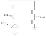
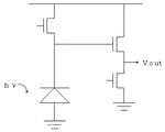
光電変換部に蓄えられた信号電荷の読み出しは、図12に示す回路構成では、光電変換部に隣接するMOS構造の電荷読出ゲート101に電圧が加えられることにより、読出ゲート101直下のポテンシャルが光電変換部のポテンシャルよりも高くなり、信号電荷が転送ゲート101に転送される。また、図13に示す回路構成例では、光電変換部の電位を直接アンプに接続し、その接続点の電位を読み出している。
In the circuit configuration shown in FIG. 12, the signal charge stored in the photoelectric conversion unit is read out by applying a voltage to the charge read
ところが、通常、光電変換部のポテンシャル構造は電荷読出方向に平坦であるため、光電変換部での電荷の転送速度は、遅く、完全に信号電荷が読み出されるには時間がかかる。また、全信号電荷を完全に読み出すことが困難である。 However, since the potential structure of the photoelectric conversion unit is generally flat in the charge reading direction, the charge transfer rate in the photoelectric conversion unit is slow, and it takes time to completely read out the signal charge. Further, it is difficult to completely read out all signal charges.
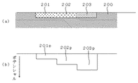
従来、固体撮像素子の製造技術としては、フォトダイオードの拡散層を複数の領域に分け、それぞれの領域の不純物濃度を変更する技術が報告されている。すなわち、図14(a)に示すように、フォトダイオード領域を3つの領域201、202、203に分け、それぞれの領域201、202、203に対して、写真製版技術とイオン注入技術を用いてP型基板200に対してN型不純物を導入する。このとき、読出方向に従って、順に不純物濃度が濃くなるように、すなわち、不純物濃度が領域203>領域202>領域201となるように、イオン注入の注入量を制御する。フォトダイオード部の領域201〜203のポテンシャル201p〜203pは、不純物濃度に依存するため、図14(b)に示すように、領域201<領域202<領域203の順に高くなるポテンシャル201p〜203pが形成される。信号電荷は、高いポテンシャルの部分へと移動するため、このような不純物濃度の変化するフォトダイオード領域201〜203からなるフォトダイオードを形成することで電荷の読み残しを無くし、また、高速な読出しを実現することができる(特許文献1参照)。
Conventionally, as a solid-state imaging device manufacturing technique, a technique has been reported in which a diffusion layer of a photodiode is divided into a plurality of regions and the impurity concentration in each region is changed. That is, as shown in FIG. 14A, the photodiode region is divided into three
しかしながら、この例では、フォトダイオード形成のための写真製版とイオン注入を複数回行う必要があり、工程数の増加に伴って、コストが高くなるとともに、個々の同一濃度領域内でのポテンシャル分布がフラットとなるため、同一濃度領域内での信号電荷の移動をさらに向上させる必要がある。 However, in this example, it is necessary to perform photoengraving and ion implantation for forming a photodiode a plurality of times, and as the number of steps increases, the cost increases and the potential distribution within each same concentration region is increased. Since it becomes flat, it is necessary to further improve the movement of signal charges within the same concentration region.
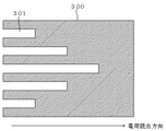
そして、従来、図15に示すように、電荷読出方向と逆方向に向かって、フォトダイオードとなる不純物拡散層300が細く枝分かれするようにレイアウトする技術が報告されている。この場合、LOCOSとなる基板領域301に寄生トランジスタの反転防止のために導入されている基板と同じ導電性の不純物がフォトダイオード拡散領域へ横方向拡散するために、電荷読出方向とは逆方向に向かってフォトダイオード拡散の実効的な不純物濃度が低下することになる。
Conventionally, as shown in FIG. 15, a technique of laying out so that the impurity diffusion layer 300 serving as a photodiode is branched in a direction opposite to the charge reading direction has been reported. In this case, the same conductive impurities as the substrate introduced to prevent the inversion of the parasitic transistor in the
したがって、読出方向と逆方向に向かって濃度が薄くなる不純物分布を作り出すことによって、図14の場合と同様に、読出方向に向かって高くなるポテンシャル分布を形成する。 Therefore, by creating an impurity distribution whose concentration decreases in the direction opposite to the reading direction, a potential distribution that increases in the reading direction is formed as in the case of FIG.
しかしながら、上記図15に示した従来技術にあっては、フォトダイオードの面積を縮小しているため、フォトダイオードの接合容量が低下して、ダイナミックレンジが縮小し、画像特性が劣化するとともに、開口率の低下によって感度が低下するという問題があった。 However, in the prior art shown in FIG. 15, since the area of the photodiode is reduced, the junction capacitance of the photodiode is reduced, the dynamic range is reduced, the image characteristics are deteriorated, and the aperture is opened. There was a problem that the sensitivity was lowered due to the decrease in the rate.
そこで、本発明は、ダイナミックレンジの低下を引き起こすことなく、残像特性の劣化を安価に抑制する固体撮像素子及び固体撮像素子の製造方法を提供することを目的としている。 Therefore, an object of the present invention is to provide a solid-state imaging device and a manufacturing method of the solid-state imaging device that can suppress deterioration of afterimage characteristics at low cost without causing a decrease in dynamic range.
具体的には、請求項1記載の発明は、第一導電型の基板領域とともに光電変換部を構成する第二導電型領域の上層に、絶縁膜を介して光透過性を有する導電性材料を形成し、当該導電性材料の電荷読出側とその反対側に電圧印加部を形成し、当該電荷読出側の電圧印加部の方が高電位となるように電圧を印加することにより、導電性材料に電位分布を持たせて、導電性材料に発生した電位に応じたポテンシャルの分布を第二導電型領域の表面付近に発生させ、光電変換部で発生した信号電荷をポテンシャルの高い電荷読出側へ移動させて、電荷の読み残しに起因する残像現象を安価に抑制するとともに、高速の読み出しを行うことのできる固体撮像素子を提供することを目的としている。 Specifically, in the first aspect of the present invention, a conductive material having light transmissivity is formed on an upper layer of the second conductivity type region constituting the photoelectric conversion portion together with the first conductivity type substrate region via an insulating film. Forming a voltage application section on the charge readout side of the conductive material and the opposite side thereof, and applying a voltage so that the voltage application section on the charge readout side has a higher potential, thereby forming the conductive material The potential distribution corresponding to the potential generated in the conductive material is generated near the surface of the second conductivity type region, and the signal charge generated in the photoelectric conversion unit is transferred to the charge readout side having a high potential. An object of the present invention is to provide a solid-state imaging device that can be moved to suppress an afterimage phenomenon caused by unread reading of charges at a low cost and perform high-speed reading.
請求項2記載の発明は、第一導電型の基板領域とともに光電変換部を構成する第二導電型領域の上層に、絶縁膜を介して光透過性を有する導電性材料を、光電変換部で光電変換された電荷の電荷読出方向に対して略直交する方向に帯状に延在して複数形成し、当該複数の導電性材料に、電荷読出側の導電性材料ほど高電位となる電圧を印加することにより、第二導電型領域に電荷読出側ほど深いポテンシャル分布を発生させて、光電変換部で発生した信号電荷をポテンシャルの高い電荷読出側に移動させて、残像現象を安価に抑制し、高速の読み出しを行えるようにするとともに、導電性材料に電流を流さないことで、消費電流を削減しつつ第二導電型領域内にポテンシャル分布を形成して、消費電流の少ない固体撮像素子を提供することを目的としている。 According to the second aspect of the present invention, an electrically conductive material having light transmittance through an insulating film is formed on the upper layer of the second conductivity type region constituting the photoelectric conversion unit together with the first conductivity type substrate region. A plurality of photoelectrically converted charges are formed in a strip shape extending in a direction substantially orthogonal to the charge readout direction, and a voltage that is higher in potential as the conductive material on the charge readout side is applied to the plurality of conductive materials. By generating a potential distribution deeper toward the charge readout side in the second conductivity type region, the signal charge generated in the photoelectric conversion unit is moved to the charge readout side having a higher potential, and the afterimage phenomenon is suppressed at a low cost, Providing a solid-state imaging device with low current consumption by enabling high-speed readout and forming a potential distribution in the second conductivity type region while reducing current consumption by preventing current from flowing through the conductive material. To do It is the target.
請求項3記載の発明は、第一導電型の基板領域上に絶縁膜を介して光透過性を有する導電性材料を形成し、当該導電性材料に電圧が印加されることで発生する空乏層を受光部として、当該導電性材料の電荷読出側とその反対側に電圧印加部を形成し、電荷読出側の電圧印加部の方が高電位となる電圧を印加することにより、導電性材料に電位分布を持たせて、導電性材料に発生した電位に応じたポテンシャルの分布を基板の表面付近に発生させ、光電変換部で発生した信号電荷をポテンシャルの高い電荷読出側へ移動させて、電荷の読み残しに起因する残像現象を安価に抑制するとともに、高速の読み出しを行うことのできる固体撮像素子を提供することを目的としている。 According to a third aspect of the present invention, a depletion layer is generated by forming a light-transmitting conductive material on a first conductive type substrate region via an insulating film and applying a voltage to the conductive material. As a light receiving part, a voltage application part is formed on the charge reading side and the opposite side of the conductive material, and a voltage that is higher in the voltage application part on the charge reading side is applied to the conductive material. A potential distribution corresponding to the potential generated in the conductive material is generated near the surface of the substrate with the potential distribution, and the signal charge generated in the photoelectric conversion unit is moved to the charge reading side having a high potential to generate the charge. An object of the present invention is to provide a solid-state imaging device capable of suppressing the afterimage phenomenon caused by the unreadness of the image at low cost and performing high-speed reading.
請求項4記載の発明は、第一導電型の基板領域上に絶縁膜を介して光透過性を有する導電性材料を形成し、当該導電性材料に電圧が印加されることで発生する空乏層を受光部として、当該導電性材料を、受光部で光電変換された電荷の電荷読出方向に対して略直交する方向に帯状に延在して複数形成し、当該複数の導電性材料に、電荷読出側の導電性材料ほど高電位となる電圧を印加することにより、基板内に電荷読出側ほど深いポテンシャル分布を発生させて、光電変換部で発生した信号電荷をポテンシャルの高い電荷読出側に移動させて、残像現象を安価に抑制し、高速の読み出しを行えるようにするとともに、導電性材料に電流を流さないことで、消費電流を削減しつつ基板内にポテンシャル分布を形成して、消費電流の少ない固体撮像素子を提供することを目的としている。 According to a fourth aspect of the present invention, a depletion layer is generated by forming a light-transmitting conductive material on a first conductivity type substrate region via an insulating film and applying a voltage to the conductive material. Are formed as a plurality of conductive materials extending in a strip shape in a direction substantially perpendicular to the charge reading direction of the charges photoelectrically converted by the light receiving portions, and charge is applied to the plurality of conductive materials. By applying a higher voltage to the readout side conductive material, a deeper potential distribution is generated in the substrate toward the charge readout side, and the signal charge generated in the photoelectric conversion unit is moved to the charge readout side with a higher potential. Therefore, the afterimage phenomenon can be suppressed at low cost and high-speed readout can be performed, and the current is not passed through the conductive material, thereby reducing the current consumption and forming a potential distribution in the substrate. Less solid photography And its object is to provide a device.
請求項5記載の発明は、請求項1から請求項4のいずれかに記載の導電性材料を、CMOSプロセスのゲート電極を形成する工程で、トランジスタのゲート電極と同時に形成することにより、安価に残像現象を抑制した固体撮像素子を製造する固体撮像素子の製造方法を提供することを目的としている。 According to a fifth aspect of the present invention, the conductive material according to any one of the first to fourth aspects is formed at the same time as the gate electrode of the transistor in the step of forming the gate electrode of the CMOS process. It aims at providing the manufacturing method of the solid-state image sensor which manufactures the solid-state image sensor which suppressed the afterimage phenomenon.
請求項1記載の発明の固体撮像素子は、第一導電型の基板領域とともに光電変換部を構成する第二導電型領域の上層に、絶縁膜を介して光透過性を有する導電性材料が形成され、当該導電性材料の電荷読出側とその反対側に電圧印加部が形成され、当該電荷読出側の電圧印加部の方に高い電圧が印加されることにより、上記目的を達成している。 In the solid-state imaging device according to the first aspect of the present invention, a light-transmitting conductive material is formed on an upper layer of the second conductive type region constituting the photoelectric conversion portion together with the first conductive type substrate region through an insulating film. In addition, a voltage application section is formed on the charge reading side and the opposite side of the conductive material, and a higher voltage is applied to the voltage reading section on the charge reading side, thereby achieving the above object.
請求項2記載の発明の固体撮像素子は、第一導電型の基板領域とともに光電変換部を構成する第二導電型領域の上層に、絶縁膜を介して光透過性を有する導電性材料が、前記光電変換部で光電変換された電荷の電荷読出方向に対して略直交する方向に帯状に延在して複数形成され、当該複数の導電性材料に、前記電荷読出側の導電性材料ほど高電位となる電圧が印加されることにより、上記目的を達成している。 In the solid-state imaging device according to the second aspect of the present invention, a conductive material having light transmittance through an insulating film is formed on the upper layer of the second conductivity type region constituting the photoelectric conversion unit together with the first conductivity type substrate region. A plurality of strips extending in a direction substantially perpendicular to the charge reading direction of charges photoelectrically converted by the photoelectric conversion unit are formed, and the higher the conductive material on the charge reading side, the higher the conductive material on the charge reading side. The above object is achieved by applying a voltage to be a potential.
請求項3記載の発明の固体撮像素子は、第一導電型の基板領域上に絶縁膜を介して光透過性を有する導電性材料が形成され、当該導電性材料に電圧が印加されることで発生する空乏層を受光部とする固体撮像素子において、前記導電性材料の電荷読出側とその反対側に電圧印加部が形成され、当該電荷読出側の電圧印加部の方に高い電圧が印加されることにより、上記目的を達成している。 According to a third aspect of the present invention, there is provided a solid-state imaging device in which a light-transmitting conductive material is formed on a first conductive type substrate region via an insulating film, and a voltage is applied to the conductive material. In a solid-state imaging device using a generated depletion layer as a light receiving portion, a voltage application portion is formed on the opposite side to the charge reading side of the conductive material, and a higher voltage is applied to the voltage reading portion on the charge reading side. The above-mentioned purpose is achieved.
請求項4記載の発明の固体撮像素子は、第一導電型の基板領域上に絶縁膜を介して光透過性を有する導電性材料が形成され、当該導電性材料に電圧が印加されることで発生する空乏層を受光部とする固体撮像素子において、前記導電性材料が、前記受光部で光電変換された電荷の電荷読出方向に対して略直交する方向に帯状に延在して複数形成され、当該複数の導電性材料に、前記電荷読出側の導電性材料ほど高電位となる電圧が印加されることにより、上記目的を達成している。 According to a fourth aspect of the present invention, there is provided a solid-state imaging device in which a light-transmitting conductive material is formed on a first conductive type substrate region via an insulating film, and a voltage is applied to the conductive material. In the solid-state imaging device using the generated depletion layer as a light receiving portion, a plurality of the conductive materials are formed to extend in a band shape in a direction substantially orthogonal to the charge reading direction of the charge photoelectrically converted by the light receiving portion. The above object is achieved by applying a voltage having a higher potential to the plurality of conductive materials as the conductive material on the charge readout side.
請求項5記載の発明の固体撮像素子の製造方法は、請求項1から請求項4のいずれかに記載の固体撮像素子を製造する固体撮像素子の製造方法であって、請求項1から請求項4のいずれかに記載の導電性材料を、CMOSプロセスのゲート電極を形成する工程で、トランジスタのゲート電極と同時に形成することにより、上記目的を達成している。 A method for manufacturing a solid-state image sensor according to a fifth aspect of the present invention is a method for manufacturing a solid-state image sensor for manufacturing the solid-state image sensor according to any one of the first to fourth aspects. The above object is achieved by forming the conductive material according to any one of 4 in the step of forming the gate electrode of the CMOS process at the same time as the gate electrode of the transistor.
請求項1記載の発明の固体撮像素子によれば、第一導電型の基板領域とともに光電変換部を構成する第二導電型領域の上層に、絶縁膜を介して光透過性を有する導電性材料を形成し、当該導電性材料の電荷読出側とその反対側に電圧印加部を形成し、当該電荷読出側の電圧印加部の方が高電位となるように電圧を印加するので、導電性材料に電位分布を持たせて、導電性材料に発生した電位に応じたポテンシャルの分布を第二導電型領域の表面付近に発生させることができ、光電変換部で発生した信号電荷をポテンシャルの高い電荷読出側へ移動させて、電荷の読み残しに起因する残像現象を安価に抑制することができるとともに、高速の読み出しを行うことができる。 According to the solid-state imaging device of the first aspect of the present invention, the conductive material having light transmissivity on the upper layer of the second conductivity type region constituting the photoelectric conversion portion together with the first conductivity type substrate region via the insulating film. Forming a voltage application portion on the charge reading side of the conductive material and the opposite side thereof, and applying a voltage so that the voltage application portion on the charge reading side has a higher potential. Potential distribution according to the potential generated in the conductive material can be generated near the surface of the second conductivity type region, and the signal charge generated in the photoelectric conversion unit can be By moving to the reading side, the afterimage phenomenon caused by the unread reading of the charges can be suppressed at a low cost, and high-speed reading can be performed.
請求項2記載の発明の固体撮像素子によれば、第一導電型の基板領域とともに光電変換部を構成する第二導電型領域の上層に、絶縁膜を介して光透過性を有する導電性材料を、光電変換部で光電変換された電荷の電荷読出方向に対して略直交する方向に帯状に延在して複数形成し、当該複数の導電性材料に、電荷読出側の導電性材料ほど高電位となる電圧を印加するので、第二導電型領域に電荷読出側ほど深いポテンシャル分布を発生させて、光電変換部で発生した信号電荷をポテンシャルの高い電荷読出側に移動させて、残像現象を安価に抑制することができ、高速の読み出しを行えるようにすることができるとともに、導電性材料に電流を流さないことで、消費電流を削減しつつ第二導電型領域内にポテンシャル分布を形成して、消費電流を削減することができる。 According to the solid-state imaging device of the second aspect of the present invention, the conductive material having optical transparency on the upper layer of the second conductivity type region constituting the photoelectric conversion portion together with the first conductivity type substrate region via the insulating film. Are formed in a strip shape extending in a direction substantially orthogonal to the charge reading direction of the charge photoelectrically converted by the photoelectric conversion unit, and the higher the conductive material on the charge reading side, the higher the conductive material on the charge reading side. Since a potential voltage is applied, a potential distribution deeper toward the charge readout side is generated in the second conductivity type region, and the signal charge generated in the photoelectric conversion unit is moved to the charge readout side having a higher potential, thereby causing an afterimage phenomenon. In addition to being able to control at low cost, it is possible to perform high-speed reading, and by not passing current through the conductive material, a potential distribution is formed in the second conductivity type region while reducing current consumption. Power consumption It can be reduced.
請求項3記載の発明の固体撮像素子によれば、第一導電型の基板領域上に絶縁膜を介して光透過性を有する導電性材料を形成し、当該導電性材料に電圧が印加されることで発生する空乏層を受光部として、当該導電性材料の電荷読出側とその反対側に電圧印加部を形成し、電荷読出側の電圧印加部の方が高電位となる電圧を印加するので、導電性材料に電位分布を持たせて、導電性材料に発生した電位に応じたポテンシャルの分布を基板の表面付近に発生させることができ、光電変換部で発生した信号電荷をポテンシャルの高い電荷読出側へ移動させて、電荷の読み残しに起因する残像現象を安価に抑制することができるとともに、高速の読み出しを行うことができる。 According to the solid-state imaging device of the third aspect of the present invention, the conductive material having optical transparency is formed on the substrate region of the first conductivity type via the insulating film, and a voltage is applied to the conductive material. Since the depletion layer generated by this is used as a light receiving part, a voltage application part is formed on the charge reading side of the conductive material and the opposite side, and the voltage application part on the charge reading side applies a higher voltage. The potential distribution according to the potential generated in the conductive material can be generated near the surface of the substrate by giving the potential distribution to the conductive material, and the signal charge generated in the photoelectric conversion unit can be By moving to the reading side, the afterimage phenomenon caused by the unread reading of the charges can be suppressed at a low cost, and high-speed reading can be performed.
請求項4記載の発明の固体撮像素子によれば、第一導電型の基板領域上に絶縁膜を介して光透過性を有する導電性材料を形成し、当該導電性材料に電圧が印加されることで発生する空乏層を受光部として、当該導電性材料を、受光部で光電変換された電荷の電荷読出方向に対して略直交する方向に帯状に延在して複数形成し、当該複数の導電性材料に、電荷読出側の導電性材料ほど高電位となる電圧を印加するので、基板内に電荷読出側ほど深いポテンシャル分布を発生させて、光電変換部で発生した信号電荷をポテンシャルの高い電荷読出側に移動させて、残像現象を安価に抑制することができ、高速の読み出しを行えるようにすることができるとともに、導電性材料に電流を流さないことで、消費電流を削減することができる。 According to the solid-state imaging device of the fourth aspect of the present invention, a conductive material having optical transparency is formed on the first conductive type substrate region via the insulating film, and a voltage is applied to the conductive material. The depletion layer generated in this way is used as a light receiving portion, and the conductive material is formed in a plurality of strips extending in a band shape in a direction substantially perpendicular to the charge reading direction of the charge photoelectrically converted by the light receiving portion. Since a voltage having a higher potential is applied to the conductive material as the conductive material on the charge reading side, a deeper potential distribution is generated in the substrate toward the charge reading side, and the signal charge generated in the photoelectric conversion unit has a higher potential. By moving to the charge readout side, the afterimage phenomenon can be suppressed at low cost, high-speed readout can be performed, and current consumption can be reduced by not passing current through the conductive material. it can.
請求項5記載の発明の固体撮像素子の製造方法によれば、請求項1から請求項4のいずれかに記載の導電性材料を、CMOSプロセスのゲート電極を形成する工程で、トランジスタのゲート電極と同時に形成しているので、安価に残像現象を抑制した固体撮像素子を製造することができる。 According to a method for manufacturing a solid-state imaging device of a fifth aspect of the present invention, the conductive material according to any one of the first to fourth aspects of the present invention is formed in a step of forming a gate electrode of a CMOS process. Since it is formed at the same time, it is possible to manufacture a solid-state imaging device that suppresses the afterimage phenomenon at low cost.
以下、本発明の好適な実施例を添付図面に基づいて詳細に説明する。なお、以下に述べる実施例は、本発明の好適な実施例であるから、技術的に好ましい種々の限定が付されているが、本発明の範囲は、以下の説明において特に本発明を限定する旨の記載がない限り、これらの態様に限られるものではない。 Hereinafter, preferred embodiments of the present invention will be described in detail with reference to the accompanying drawings. In addition, since the Example described below is a suitable Example of this invention, various technically preferable restrictions are attached | subjected, However, The scope of the present invention limits this invention especially in the following description. As long as there is no description of the effect, it is not restricted to these aspects.
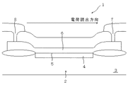
図1〜図4は、本発明の固体撮像素子及び固体撮像素子の製造方法の第1実施例を示す図であり、図1は、本発明の固体撮像素子及び固体撮像素子の製造方法の第1実施例を適用した固体撮像素子1の平面図、図2は、図1のA−A矢視断面図である。
1 to 4 are diagrams showing a first embodiment of a solid-state imaging device and a manufacturing method of the solid-state imaging device according to the present invention. FIG. 1 shows a first example of the solid-state imaging device and the manufacturing method of the solid-state imaging device according to the present invention. 1 is a plan view of a solid-
図1及び図2において、固体撮像素子1は、光電変換部2を構成する第一導電型の基板領域(P)3と第二導電型(N−)領域4の上層に、絶縁膜5を介して光透過性を有する導電性材料(電極)6が配置されている。固体撮像素子1は、この導電性材料6のフォトダイオードの電荷読出側に電圧印加部7が設けられており、電圧印加部7とは反対側に、電圧印加部8が設けられている。
1 and 2, the solid-
固体撮像素子1は、導電性材料6を、従来のCMOSプロセスで用いられるトランジスタの電極となるポリシリコンを形成する工程と同時に形成している。この場合、ポリシリコンによる光の吸収が、固体撮像素子1の感度に影響を及ぼさない程度に、ポリシリコン層の膜厚を制御する。
In the solid-
また、フォトダイオードの上層に絶縁膜5を介して配置する導電性材料6としては、ポリシリコン以外に、ITO、SnO2 、ZnO等の透明電極材料を用いてもよい。
Further, as the
この固体撮像素子1は、電圧印加部7に、電圧印加部8に対して、電圧印加部7>電圧印加部8となる電圧が印加されると、導電性材料6に電流が流れる。
In the solid-
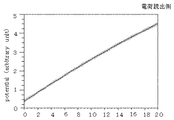
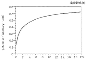
このとき、導電性材料6がある電気抵抗を持っているため、導電性材料6の電位は、図3に示すように、電圧印加部8側から電圧印加部7側方向に向かって順次増大する。この導電性材料6の電位によって発生する基板内の第二導電型(N−)領域4の表面付近のポテンシャルは、図4に示すように、電圧印加部8側から電圧印加部7側に向かって徐々に高くなる。
At this time, since the
したがって、光照射によって発生した電荷は、このポテンシャルの傾斜に沿って、電荷読出側へと移動する。 Therefore, the charge generated by the light irradiation moves to the charge reading side along this potential gradient.
このように、本実施例の固体撮像素子1は、第一導電型の基板領域3とともに光電変換部2を構成する第二導電型領域4の上層に、絶縁膜5を介して光透過性を有する導電性材料6を形成し、当該導電性材料6の電荷読出側とその反対側に電圧印加部7と電圧印加部8を形成し、電圧印加部7と電圧印加部8に、当該電圧印加部7が当該電圧印加部8よりも高電位となる電圧を印加している。
As described above, the solid-
したがって、導電性材料6に電位分布を持たせて、導電性材料6に発生した電位に応じたポテンシャルの分布を第二導電型領域4の表面付近に発生させることができ、光電変換部2で発生した信号電荷をポテンシャルの高い電荷読出側へ移動させて、電荷の読み残しに起因する残像現象を安価に抑制することができるとともに、高速の読み出しを行うことができる。
Therefore, the
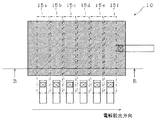
図5〜図7は、本発明の固体撮像素子及び固体撮像素子の製造方法の第2実施例を示す図であり、図5は、本発明の固体撮像素子及び固体撮像素子の製造方法の第2実施例を適用した固体撮像素子10の平面図、図6は、図5のB−B矢視断面図である。
5 to 7 are diagrams showing a second embodiment of the solid-state imaging device and the manufacturing method of the solid-state imaging device of the present invention, and FIG. 5 is a diagram of the solid-state imaging device of the present invention and the manufacturing method of the solid-state imaging device. FIG. 6 is a plan view of the solid-
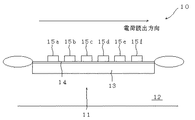
図5及び図6において、固体撮像素子10は、光電変換部11が第一導電型の基板領域12と第二導電型(N−)領域13で構成されており、この第二導電型(N−)領域13の上層に、絶縁膜14を介して光透過性を持つ帯状の導電性材料による電極15a〜15fが複数形成されている。これらの電極15a〜15fは、読出方向に近づくほど順次高い電圧が与えられる。
5 and 6, in the solid-
固体撮像素子10は、導電性材料の電極15a〜15fを、従来のCMOSプロセスで用いられるトランジスタの電極となるポリシリコンを形成する工程と同時に形成している。この場合、ポリシリコンによる光の吸収が、固体撮像素子10の感度に影響を及ぼさない程度に、ポリシリコン層の膜厚を制御する。
In the solid-
また、フォトダイオードの上層に絶縁膜14を介して配置する電極15a〜15fとなる導電性材料としては、ポリシリコン以外に、ITO、SnO2 、ZnO等の透明電極材料を用いてもよい。
In addition to polysilicon, a transparent electrode material such as ITO, SnO 2 , or ZnO may be used as the conductive material that becomes the electrodes 15 a to 15 f disposed above the photodiode via the insulating
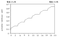
固体撮像素子10は、光電変換部11を構成する第一導電型の基板領域12と第二導電型(N−)領域13の上層に、絶縁膜14を介して形成された導電性材料の電極15a〜15fに読出方向ほど順次高い電位が与えられると、図7に示すように、読出方向に近づくほど、すなわち、電極15aから電極15fへと移動するに従って、高い階段状のポテンシャル分布を得ることができ、読出側へ光信号電荷を移動させることができる。
The solid-
このように、本実施例の固体撮像素子10は、第一導電型の基板領域12とともに光電変換部11を構成する第二導電型領域13の上層に、絶縁膜14を介して光透過性を有する導電性材料の電極15a〜15fを、光電変換部11で光電変換された電荷の電荷読出方向に対して略直交する方向に帯状に延在して複数形成し、当該複数の導電性材料の電極15a〜15fに、電荷読出側の導電性材料の電極15a〜15fほど高電位となる電圧を印加している。
As described above, the solid-
したがって、第二導電型領域13に電荷読出側ほど深いポテンシャル分布を発生させて、光電変換部11で発生した信号電荷をポテンシャルの高い電荷読出側に移動させて、残像現象を安価に抑制することができ、高速の読み出しを行えるようにすることができるとともに、導電性材料の電極15a〜15fに電流を流さないことで、消費電流を削減しつつ第二導電型領域13内にポテンシャル分布を形成して、消費電流を削減することができる。
Therefore, a deeper potential distribution is generated in the second
図8及び図9は、本発明の固体撮像素子及び固体撮像素子の製造方法の第3実施例を示す図であり、図8は、本発明の固体撮像素子及び固体撮像素子の製造方法の第3実施例を適用した固体撮像素子20の平面図、図9は、図8のC−C矢視断面図である。
8 and 9 are diagrams showing a third embodiment of the solid-state imaging device and the method for manufacturing the solid-state imaging device according to the present invention, and FIG. 8 is a diagram illustrating the solid-state imaging device and the method for manufacturing the solid-state imaging device according to the present invention. FIG. 9 is a cross-sectional view taken along the line CC in FIG. 8. FIG. 9 is a plan view of the solid-
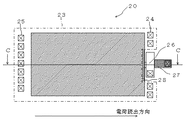
図8及び図9において、固体撮像素子20は、第一導電型の基板領域(P)21上に、第二導電型層を設けることなく、絶縁膜22を介して光透過性を有する導電性材料の電極23が設けられており、この導電性材料の電極23の電荷読出側とその反対側に電圧印加部24と電圧印加部25が形成され、当該電圧印加部24が当該電圧印加部25よりも高電位となる電圧が印加される。
8 and 9, the solid-
固体撮像素子20は、電荷読出部29側には、導電性材料の電極23と所定間隔空けて読出ゲート26が形成されており、第一導電型の基板領域(P)21には、読出ゲート26を挟んで、導電性材料の電極23側と電荷読出部29側に拡散層28と拡散層27が形成されている。
In the solid-
すなわち、この固体撮像素子20は、基板21上に絶縁膜22を介して配置された導電性材料の電極23に電圧印加することで発生する基板21の表面の空乏層を光検出部とする固体撮像素子である。
That is, the solid-
そして、固体撮像素子20は、導電性材料の電極23を、従来のCMOSプロセスで用いられるトランジスタの電極となるポリシリコンを形成する工程と同時に形成している。この場合、ポリシリコンによる光の吸収が、固体撮像素子20の感度に影響を及ぼさない程度に、ポリシリコン層の膜厚を制御する。
In the solid-
また、フォトダイオードの上層に絶縁膜22を介して配置する電極23となる導電性材料としては、ポリシリコン以外に、ITO、SnO2 、ZnO等の透明電極材料を用いてもよい。
In addition to polysilicon, a transparent electrode material such as ITO, SnO 2 , or ZnO may be used as the conductive material that becomes the electrode 23 disposed on the upper layer of the photodiode via the insulating
この固体撮像素子20は、電圧印加部24と電圧印加部25に、電圧印加部24の方が高電位となる電圧が印加されて、導電性材料の電極23にポテンシャル分布が発生すると、基板21の表面付近に発生するポテンシャルに傾斜が発生し、電荷読出側に光信号電荷が移動する。この信号電荷は、拡散層28に移動した後、読出ゲート26に電圧が加えられることにより、拡散層27に転送され、後段のアンプへ出力される。
In the solid-
このように、本実施例の固体撮像素子20は、第一導電型の基板領域21上に絶縁膜22を介して光透過性を有する導電性材料で電極23を形成し、当該導電性材料の電極23に電圧が印加されることで発生する空乏層を受光部として、当該導電性材料の電荷読出側とその反対側に、電圧印加部24と電圧印加部25を形成し、電圧印加部24と電圧印加部25に、当該電圧印加部24が当該電圧印加部25よりも高電位となる電圧を印加している。
As described above, the solid-
したがって、導電性材料の電極23に電位分布を持たせて、導電性材料の電極23に発生した電位に応じたポテンシャルの分布を基板領域21の表面付近に発生させることができ、光電変換部で発生した信号電荷をポテンシャルの高い電荷読出側へ移動させて、電荷の読み残しに起因する残像現象を安価に抑制することができるとともに、高速の読み出しを行うことができる。
Therefore, the potential distribution can be generated in the vicinity of the surface of the
図10〜図11は、本発明の固体撮像素子及び固体撮像素子の製造方法の第4実施例を示す図であり、図10は、本発明の固体撮像素子及び固体撮像素子の製造方法の第4実施例を適用した固体撮像素子30の平面図、図11は、図10のD−D矢視断面図である。
10 to 11 are diagrams showing a fourth embodiment of the solid-state imaging device and the manufacturing method of the solid-state imaging device of the present invention, and FIG. 10 is a diagram of the solid-state imaging device of the present invention and the manufacturing method of the solid-state imaging device. The top view of the solid-
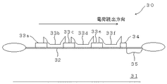
図10及び図11において、固体撮像素子30は、第一導電型の基板領域(P)31上に、第二導電型層を設けることなく、絶縁膜32を介して光透過性を有する導電性材料により複数の電極33a〜33fが形成されており、この導電性材料の電極33a〜33fの電荷読出側に電荷読出ゲート34が設けられている。固体撮像素子30は、電荷読出ゲート34の受光部と反対側には拡散層35が形成される。
10 and 11, the solid-
固体撮像素子30は、導電性材料の電極33a〜33fを、従来のCMOSプロセスで用いられるトランジスタの電極となるポリシリコンを形成する工程と同時に形成している。この場合、ポリシリコンによる光の吸収が、固体撮像素子30の感度に影響を及ぼさない程度に、ポリシリコン層の膜厚を制御する。
In the solid-
また、フォトダイオードの上層に絶縁膜32を介して配置する電極33a〜33fとなる導電性材料としては、ポリシリコン以外に、ITO、SnO2 、ZnO等の透明電極材料を用いてもよい。
In addition to polysilicon, a transparent electrode material such as ITO, SnO 2 , or ZnO may be used as the conductive material that becomes the electrodes 33a to 33f disposed above the photodiode via the insulating
そして、固体撮像素子30は、導電性材料の電極33a〜33fに読出方向に向かって順次高くなる電圧を与えると、図7と同様に、読出方向に近づくほど深い階段状のポテンシャル分布を得ることができる。したがって、電荷読出ゲート34に電圧印加することで、信号電荷が容易に拡散層35へ転送される。
Then, when the solid-
このように、本実施例の固体撮像素子30は、第一導電型の基板領域31上に絶縁膜32を介して光透過性を有する導電性材料で電極33a〜33fを形成し、導電性材料の電極33a〜33fに電圧が印加されることで発生する空乏層を受光部として、当該導電性材料の電極33a〜33fを、受光部で光電変換された電荷の電荷読出方向に対して略直交する方向に帯状に延在して複数形成し、当該複数の導電性材料の電極33a〜33fに、電荷読出側の導電性材料の電極ほど高電位となる電圧を印加している。
As described above, the solid-
したがって、基板31に電荷読出側ほど深いポテンシャル分布を発生させて、光電変換部で発生した信号電荷をポテンシャルの高い電荷読出側に移動させて、残像現象を安価に抑制することができ、高速の読み出しを行えるようにすることができるとともに、導電性材料に電流を流さないことで、消費電流を削減しつつ基板31内にポテンシャル分布を形成することができる。
Accordingly, a deeper potential distribution is generated on the charge reading side on the
そして、各実施例において、導電性材料6、15a〜15f、23、33a〜33fを、CMOSプロセスのゲート電極を形成する工程で、トランジスタのゲート電極と同時に形成している。したがって、残像現象を抑制した固体撮像素子1、10、20、30を安価に製造することができる。
In each embodiment, the
以上、本発明者によってなされた発明を好適な実施例に基づき具体的に説明したが、本発明は上記のものに限定されるものではなく、その要旨を逸脱しない範囲で種々変更可能であることはいうまでもない。 The invention made by the present inventor has been specifically described based on the preferred embodiments. However, the present invention is not limited to the above, and various modifications can be made without departing from the scope of the invention. Needless to say.
ダイナミックレンジの低下を引き起こすことなく、残像特性を抑制し高速動作可能な固体撮像素子及び固体撮像素子の製造方法に適用することができる。 The present invention can be applied to a solid-state imaging device capable of suppressing an afterimage characteristic and operating at high speed without causing a decrease in dynamic range and a method for manufacturing the solid-state imaging device.
1 固体撮像素子
2 光電変換部
3 第一導電型基板領域(P)
4 第二導電型(N−)領域
5 絶縁膜
6 導電性材料
7 電圧印加部
8 電圧印加部
10 固体撮像素子
11 光電変換部
12 第一導電型基板領域
13 第二導電型(N−)領域
14 絶縁膜
15a〜15f 電極
20 固体撮像素子
21 第一導電型基板領域(P)
22 絶縁膜
23 電極
24 電圧印加部
25 電圧印加部
26 読出ゲート
27、28 拡散層
29 電位読出部
30 固体撮像素子
31 第一導電型基板領域(P)
32 絶縁膜
33a〜33f 電極
34 電荷読出ゲート
35 拡散層
DESCRIPTION OF
DESCRIPTION OF
DESCRIPTION OF
32 Insulating film 33a to
Claims (5)
5. A method of manufacturing a solid-state imaging device for manufacturing the solid-state imaging device according to claim 1, wherein the conductive material according to any one of claims 1 to 4 is used in a CMOS process. A method for manufacturing a solid-state imaging device, wherein the step of forming a gate electrode is performed simultaneously with a gate electrode of a transistor.
Priority Applications (1)
| Application Number | Priority Date | Filing Date | Title |
|---|---|---|---|
| JP2004079553A JP2005268564A (en) | 2004-03-19 | 2004-03-19 | Solid-state imaging device and manufacturing method of solid-state imaging device |
Applications Claiming Priority (1)
| Application Number | Priority Date | Filing Date | Title |
|---|---|---|---|
| JP2004079553A JP2005268564A (en) | 2004-03-19 | 2004-03-19 | Solid-state imaging device and manufacturing method of solid-state imaging device |
Publications (1)
| Publication Number | Publication Date |
|---|---|
| JP2005268564A true JP2005268564A (en) | 2005-09-29 |
Family
ID=35092789
Family Applications (1)
| Application Number | Title | Priority Date | Filing Date |
|---|---|---|---|
| JP2004079553A Pending JP2005268564A (en) | 2004-03-19 | 2004-03-19 | Solid-state imaging device and manufacturing method of solid-state imaging device |
Country Status (1)
| Country | Link |
|---|---|
| JP (1) | JP2005268564A (en) |
Cited By (7)
| Publication number | Priority date | Publication date | Assignee | Title |
|---|---|---|---|---|
| WO2008066067A1 (en) | 2006-11-28 | 2008-06-05 | Hamamatsu Photonics K.K. | Solid-state imaging element |
| JP2009231768A (en) * | 2008-03-25 | 2009-10-08 | Hamamatsu Photonics Kk | Solid-state imaging device |
| WO2009133799A1 (en) * | 2008-04-30 | 2009-11-05 | 浜松ホトニクス株式会社 | Solid-state imaging device |
| US7619196B2 (en) | 2006-01-31 | 2009-11-17 | Sanyo Electric Co., Ltd. | Imaging device including a multiplier electrode |
| WO2012096051A1 (en) | 2011-01-14 | 2012-07-19 | 浜松ホトニクス株式会社 | Solid state imaging device |
| US9419051B2 (en) | 2011-01-20 | 2016-08-16 | Hamamatsu Photonics K.K. | Solid-state imaging device |
| JPWO2020039531A1 (en) * | 2018-08-23 | 2021-08-26 | 国立大学法人東北大学 | Optical sensor and its signal reading method and optical area sensor and its signal reading method |
-
2004
- 2004-03-19 JP JP2004079553A patent/JP2005268564A/en active Pending
Cited By (17)
| Publication number | Priority date | Publication date | Assignee | Title |
|---|---|---|---|---|
| US7619196B2 (en) | 2006-01-31 | 2009-11-17 | Sanyo Electric Co., Ltd. | Imaging device including a multiplier electrode |
| EP2093801B1 (en) * | 2006-11-28 | 2016-11-16 | Hamamatsu Photonics K.K. | Solid-state imaging element |
| JP5350803B2 (en) * | 2006-11-28 | 2013-11-27 | 浜松ホトニクス株式会社 | Solid-state image sensor |
| WO2008066067A1 (en) | 2006-11-28 | 2008-06-05 | Hamamatsu Photonics K.K. | Solid-state imaging element |
| US8334918B2 (en) | 2006-11-28 | 2012-12-18 | Hamamatsu Photonics K.K. | Solid-state imaging element |
| US8415604B2 (en) | 2008-03-25 | 2013-04-09 | Hamamatsu Photonics K.K. | Solid-state imaging device |
| JP2009231768A (en) * | 2008-03-25 | 2009-10-08 | Hamamatsu Photonics Kk | Solid-state imaging device |
| US8446500B2 (en) | 2008-04-30 | 2013-05-21 | Hamamatsu Photonics K.K. | Solid-state imaging device having photoelectric converting portions and first and second transfer portions |
| JP2009272333A (en) * | 2008-04-30 | 2009-11-19 | Hamamatsu Photonics Kk | Solid state imaging device |
| WO2009133799A1 (en) * | 2008-04-30 | 2009-11-05 | 浜松ホトニクス株式会社 | Solid-state imaging device |
| WO2012096051A1 (en) | 2011-01-14 | 2012-07-19 | 浜松ホトニクス株式会社 | Solid state imaging device |
| KR20140001906A (en) | 2011-01-14 | 2014-01-07 | 하마마츠 포토닉스 가부시키가이샤 | Solid state imaging device |
| US8841714B2 (en) | 2011-01-14 | 2014-09-23 | Hamamatsu Photonics K.K. | Solid state imaging device |
| TWI563644B (en) * | 2011-01-14 | 2016-12-21 | Hamamatsu Photonics Kk | |
| US9419051B2 (en) | 2011-01-20 | 2016-08-16 | Hamamatsu Photonics K.K. | Solid-state imaging device |
| JPWO2020039531A1 (en) * | 2018-08-23 | 2021-08-26 | 国立大学法人東北大学 | Optical sensor and its signal reading method and optical area sensor and its signal reading method |
| JP7333562B2 (en) | 2018-08-23 | 2023-08-25 | 国立大学法人東北大学 | Optical sensor and its signal readout method and optical area sensor and its signal readout method |
Similar Documents
| Publication | Publication Date | Title |
|---|---|---|
| US7205568B2 (en) | Solid state image pickup apparatus and radiation image pickup apparatus | |
| US10074678B2 (en) | Solid-state imaging device and electronic apparatus | |
| CN103329271B (en) | solid state imaging device | |
| US8610234B2 (en) | Unit pixel of image sensor and photo detector thereof | |
| US7154137B2 (en) | Image sensor and pixel having a non-convex photodiode | |
| JP2013030820A (en) | Solid-state image pickup device | |
| US10957726B2 (en) | Image sensors having a reduced settling time | |
| CN104835825A (en) | High-speed CMOS image sensor | |
| KR20100135217A (en) | Solid-state imaging device | |
| JP2008153427A (en) | High-sensitivity photosensor element and photosensor device using the same | |
| JP4130307B2 (en) | Solid-state imaging device | |
| JP2005268564A (en) | Solid-state imaging device and manufacturing method of solid-state imaging device | |
| JP6739891B2 (en) | Solid-state imaging device | |
| JP2006157000A (en) | CMOS image sensor with buried channel MOS transistor | |
| JPH0454988B2 (en) | ||
| JPH09275201A (en) | Solid-state image pick up device | |
| JP5350659B2 (en) | Solid-state imaging device | |
| US11901465B2 (en) | Optical sensor | |
| JP2000049322A (en) | MOS transistor for photocell | |
| CN110634902B (en) | An ultra-high-speed shutter semiconductor image sensor | |
| JPH0414547B2 (en) | ||
| CN111211138B (en) | A pixel unit, sensor and sensing array | |
| JP2006086232A (en) | MOS type solid-state imaging device, camera | |
| JPH0682823B2 (en) | Solid-state imaging device | |
| KR20230009400A (en) | Optical detection device and optical sensor driving method |
Legal Events
| Date | Code | Title | Description |
|---|---|---|---|
| A521 | Request for written amendment filed |
Free format text: JAPANESE INTERMEDIATE CODE: A523 Effective date: 20050621 |
|
| A871 | Explanation of circumstances concerning accelerated examination |
Free format text: JAPANESE INTERMEDIATE CODE: A871 Effective date: 20050621 |
|
| A975 | Report on accelerated examination |
Free format text: JAPANESE INTERMEDIATE CODE: A971005 Effective date: 20050715 |
|
| A131 | Notification of reasons for refusal |
Free format text: JAPANESE INTERMEDIATE CODE: A131 Effective date: 20050726 |
|
| A521 | Request for written amendment filed |
Free format text: JAPANESE INTERMEDIATE CODE: A523 Effective date: 20050922 |
|
| A02 | Decision of refusal |
Free format text: JAPANESE INTERMEDIATE CODE: A02 Effective date: 20060314 |