JP2005266083A - Device and method for observation - Google Patents
Device and method for observation Download PDFInfo
- Publication number
- JP2005266083A JP2005266083A JP2004076267A JP2004076267A JP2005266083A JP 2005266083 A JP2005266083 A JP 2005266083A JP 2004076267 A JP2004076267 A JP 2004076267A JP 2004076267 A JP2004076267 A JP 2004076267A JP 2005266083 A JP2005266083 A JP 2005266083A
- Authority
- JP
- Japan
- Prior art keywords
- objective lens
- observation
- substrate
- magnification
- optical path
- Prior art date
- Legal status (The legal status is an assumption and is not a legal conclusion. Google has not performed a legal analysis and makes no representation as to the accuracy of the status listed.)
- Pending
Links
Images


Classifications
-
- G—PHYSICS
- G02—OPTICS
- G02B—OPTICAL ELEMENTS, SYSTEMS OR APPARATUS
- G02B21/00—Microscopes
- G02B21/0004—Microscopes specially adapted for specific applications
- G02B21/0016—Technical microscopes, e.g. for inspection or measuring in industrial production processes
-
- G—PHYSICS
- G01—MEASURING; TESTING
- G01N—INVESTIGATING OR ANALYSING MATERIALS BY DETERMINING THEIR CHEMICAL OR PHYSICAL PROPERTIES
- G01N21/00—Investigating or analysing materials by the use of optical means, i.e. using sub-millimetre waves, infrared, visible or ultraviolet light
- G01N21/84—Systems specially adapted for particular applications
- G01N21/88—Investigating the presence of flaws or contamination
- G01N21/95—Investigating the presence of flaws or contamination characterised by the material or shape of the object to be examined
- G01N21/9501—Semiconductor wafers
-
- G—PHYSICS
- G01—MEASURING; TESTING
- G01B—MEASURING LENGTH, THICKNESS OR SIMILAR LINEAR DIMENSIONS; MEASURING ANGLES; MEASURING AREAS; MEASURING IRREGULARITIES OF SURFACES OR CONTOURS
- G01B9/00—Measuring instruments characterised by the use of optical techniques
- G01B9/04—Measuring microscopes
-
- G—PHYSICS
- G02—OPTICS
- G02B—OPTICAL ELEMENTS, SYSTEMS OR APPARATUS
- G02B21/00—Microscopes
- G02B21/02—Objectives
Abstract
Description
この発明は、半導体ウエハや液晶等のデバイス等の基板を拡大して観察する観察装置に関するものである。 The present invention relates to an observation apparatus for magnifying and observing a substrate such as a semiconductor wafer or a liquid crystal device.
半導体デバイスの製造工程において、半導体ウエハ(基板)の表面にデバイスパターンを形成する際には、異物の付着、パターンの欠陥や寸法異常等の欠陥が発生することがあるため、その欠陥内容を識別する必要がある。具体的には、基板全体を目視で行う外観検査や、ラインセンサを用いた検査が行われ、欠陥箇所を検出する。そして、この欠陥内容の識別には、半導体ウエハの表面を拡大観察する機能を備えた検査装置(観察装置)が用いられる。
この検査装置には、倍率が異なる複数の対物レンズが設けられている。半導体ウエハの表面に形成された回路パターンを拡大観察する際には、任意の対物レンズを観察光路内に挿入し、半導体ウエハの表面の観察位置に対向させて配する。ここで、対物レンズの焦点距離は、対物レンズの倍率が高くなる程小さくなるため、高倍率の対物レンズを使用する際には、対物レンズと半導体ウエハとの隙間が小さくなる。すなわち、例えば、光源に紫外線を用いて高倍率、高分解能の拡大観察を行う場合には、紫外線用の対物レンズを使用するが、この対物レンズのワーキングディスタンス(WD、作動距離)は0.2〜0.3mmである。なお、半導体ウエハ表面の拡大観察位置を変更する場合には、対物レンズを半導体ウエハの表面に沿う方向に移動させる。
In semiconductor device manufacturing processes, when device patterns are formed on the surface of a semiconductor wafer (substrate), defects such as adhesion of foreign matter, pattern defects, and dimensional abnormalities may occur. There is a need to. Specifically, an appearance inspection for visually checking the entire substrate and an inspection using a line sensor are performed to detect a defective portion. An inspection device (observation device) having a function of magnifying and observing the surface of the semiconductor wafer is used for identifying the defect contents.
This inspection apparatus is provided with a plurality of objective lenses having different magnifications. When magnifying and observing the circuit pattern formed on the surface of the semiconductor wafer, an arbitrary objective lens is inserted into the observation optical path and arranged facing the observation position on the surface of the semiconductor wafer. Here, since the focal length of the objective lens becomes smaller as the magnification of the objective lens becomes higher, the gap between the objective lens and the semiconductor wafer becomes smaller when a high magnification objective lens is used. That is, for example, when performing high-magnification and high-resolution magnification observation using ultraviolet light as a light source, an ultraviolet objective lens is used, and the working distance (WD, working distance) of this objective lens is 0.2. ~ 0.3 mm. When changing the magnification observation position on the surface of the semiconductor wafer, the objective lens is moved in a direction along the surface of the semiconductor wafer.
ところで、半導体デバイスを製造する工程においては、半導体ウエハに反りや撓みが発生する。このため、対物レンズを半導体ウエハの表面に沿って移動させた際には、対物レンズと半導体ウエハとの隙間が、対物レンズのWDよりも狭くなる場合がある。
そこで、従来の検査装置としては、対物レンズと半導体ウエハとの接触を回避するために、対物レンズから半導体ウエハまでの距離を測定する距離センサ等を各対物レンズ設けて、対物レンズと半導体ウエハとの隙間を一定に保持するものがある(例えば、特許文献1参照。)。
また、従来の検査装置には、半導体ウエハを載置する載置ステージとして半導体ウエハの裏面全体を真空吸着させる全面吸着プレートを使用し、この吸着力により半導体ウエハの反りや撓みを矯正するように構成したものもある。
Therefore, as a conventional inspection apparatus, in order to avoid contact between the objective lens and the semiconductor wafer, each objective lens is provided with a distance sensor or the like for measuring the distance from the objective lens to the semiconductor wafer. There is one that keeps the gap between them constant (for example, see Patent Document 1).
In addition, the conventional inspection apparatus uses a full-surface suction plate that vacuum-sucks the entire back surface of the semiconductor wafer as a mounting stage for mounting the semiconductor wafer, and corrects the warping and bending of the semiconductor wafer by this suction force. Some are configured.
しかしながら、上記従来の検査装置には、複雑で高価な距離センサ、全面吸着プレートを設けていたため、検査装置の製造コストが高くなるという問題がある。
この発明は上述した事情に鑑みてなされたものであって、対物レンズと半導体ウエハとの接触を回避できると共に、製造コストの削減を図ることができる検査装置及び検査方法を提供することを目的としている。
However, the conventional inspection apparatus is provided with a complicated and expensive distance sensor and a full-surface suction plate, and thus there is a problem that the manufacturing cost of the inspection apparatus increases.
The present invention has been made in view of the above-described circumstances, and an object thereof is to provide an inspection apparatus and an inspection method that can avoid contact between the objective lens and the semiconductor wafer and can reduce manufacturing costs. Yes.
上記目的を達成するために、この発明は、以下の手段を提供する。
請求項1に係る発明は、対物レンズを用いて基板の表面を拡大して観察を行う観察装置であって、倍率の異なる複数の対物レンズを装着したレボルバと、前記レボルバを動作させて観察光路内に挿入する前記対物レンズを切り換える対物レンズ切換手段と、前記観察光路内に挿入された前記対物レンズに対向して設けられ、前記基板の表面が前記観察光路の光軸に略直交するように前記基板を載置する載置ステージと、前記観察光路内に挿入された前記対物レンズの倍率を検出する対物レンズ検出手段と、前記観察光路の光軸方向及び該光軸の直交方向に前記対物レンズと前記載置ステージとを相対的に移動させる移動手段と、前記レンズ検出手段が所定倍率よりも高い倍率の対物レンズを検出した際に、前記直交方向に関して前記移動手段による前記対物レンズと前記載置ステージとの相対移動を規制する移動制御手段とを備えることを特徴とする観察装置を提供する。
In order to achieve the above object, the present invention provides the following means.
The invention according to
請求項2に係る発明は、請求項1に記載の観察装置において、前記移動制御手段が、前記対物レンズと前記載置ステージとの相対的な移動範囲を限定することを特徴とする観察装置を提供する。
The invention according to
請求項3に係る発明は、請求項1又は請求項2に記載の観察装置において、前記移動制御手段が、前記対物レンズと前記載置ステージとの相対的な移動速度を所定の速度よりも遅い速度に限定することを特徴とする観察装置を提供する。 According to a third aspect of the present invention, in the observation apparatus according to the first or second aspect, the movement control means has a relative moving speed of the objective lens and the mounting stage slower than a predetermined speed. Provided is an observation apparatus characterized by being limited to speed.
請求項4に係る発明は、請求項1に記載の観察装置において、前記移動制御手段が、前記対物レンズと前記載置ステージとの相対的な移動を禁止することを特徴とする観察装置を提供する。
The invention according to
請求項5に係る発明は、倍率の異なる複数の対物レンズを適宜選択して基板の表面の拡大観察を行う基板の観察方法であって、前記基板の表面を前記対物レンズの焦点位置に配するように、前記基板の表面に略直交する前記対物レンズの光軸方向に前記対物レンズと前記基板とを相対的に移動させるピント合わせ工程と、前記光軸の直交方向に前記対物レンズと前記基板とを相対的に移動させて、前記基板表面の拡大観察位置を変更する観察位置移動工程とを備え、所定倍率よりも高い倍率の前記対物レンズを用いて前記基板の拡大観察を行う際に、前記観察位置移動工程における前記対物レンズと前記基板との相対的な移動を規制することを特徴とする基板の観察方法を提供する。 The invention according to claim 5 is a substrate observation method for appropriately magnifying and observing the surface of the substrate by appropriately selecting a plurality of objective lenses having different magnifications, and arranging the surface of the substrate at a focal position of the objective lens. A focusing step of relatively moving the objective lens and the substrate in an optical axis direction of the objective lens substantially orthogonal to the surface of the substrate, and the objective lens and the substrate in a direction orthogonal to the optical axis And performing an enlarged observation of the substrate using the objective lens having a magnification higher than a predetermined magnification, and an observation position moving step of changing an enlarged observation position of the substrate surface. A substrate observation method is provided, wherein relative movement between the objective lens and the substrate in the observation position moving step is regulated.
本発明の観察装置及び観察方法によれば、所定倍率よりも高い倍率の対物レンズ、すなわち焦点距離が所定長さよりも小さい高倍率の対物レンズを選択して基板の拡大観察を行う場合には、光軸の直交方向に関する対物レンズと基板との相対的な移動、特に、光軸の直交方向の移動範囲や移動速度が規制されるため、基板の反りや撓みに基づいて対物レンズと基板とが接触することを回避できる。 According to the observation apparatus and the observation method of the present invention, when an objective lens having a magnification higher than a predetermined magnification, that is, an objective lens having a high magnification whose focal length is smaller than a predetermined length is selected to perform magnified observation of the substrate, The relative movement between the objective lens and the substrate in the direction perpendicular to the optical axis, in particular, the movement range and movement speed in the direction orthogonal to the optical axis are regulated. Contact can be avoided.
また、対物レンズと基板との接触を防止するために、対物レンズと基板との距離を測定する距離センサや、基板の反り・撓みを矯正する全面吸着プレート等を新たに設ける必要が無いため、観察装置の製造コストの削減を図ることができる。
さらに、本発明の観察装置によれば、移動制御手段が移動手段による対物レンズと載置ステージとの相対的な移動を禁止する場合には、高い倍率の対物レンズを選択して基板の拡大観察を行う際に、対物レンズと基板との接触を確実に防止できる。
In addition, in order to prevent contact between the objective lens and the substrate, it is not necessary to newly provide a distance sensor for measuring the distance between the objective lens and the substrate, a full-surface suction plate for correcting the warp / deflection of the substrate, etc. The manufacturing cost of the observation apparatus can be reduced.
Further, according to the observation apparatus of the present invention, when the movement control unit prohibits the relative movement between the objective lens and the mounting stage by the moving unit, the objective lens having a high magnification is selected and the substrate is enlarged and observed. When performing, the contact between the objective lens and the substrate can be surely prevented.
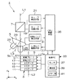
図1から図4は本発明に係る一実施形態を示しており、ここで説明する実施の形態は、この発明を半導体ウエハの表面に形成されたパターンの欠陥を拡大観察して検査を行うウエハ検査装置に適用した場合のものである。図1に示すように、この検査装置(観察装置)1は、半導体ウエハSの表面Saを観察するための可視光線やDUV等の紫外線が通過する観察光路の光軸L1方向に順次配された試料ステージ部3、レボルバ部5及びフィルターユニット7を備えている。
なお、レボルバ部5及びフィルターユニット7を順次通過した可視光線や紫外線は、半導体ウエハSの表面Saを観察する領域の画像を取得するCCDカメラや、この観察領域を視認する接眼レンズ等の観察部(図示せず)に入射される。
1 to 4 show an embodiment according to the present invention. In the embodiment described here, a wafer in which the present invention is inspected by magnifying and observing a defect of a pattern formed on the surface of a semiconductor wafer. When applied to an inspection device. As shown in FIG. 1, the inspection apparatus (observation apparatus) 1 is sequentially arranged in the direction of the optical axis L1 of an observation optical path through which ultraviolet rays such as visible rays and DUV for observing the surface Sa of the semiconductor wafer S pass. A sample stage unit 3, a revolver unit 5, and a
The visible light and the ultraviolet rays that have passed through the revolver unit 5 and the
試料ステージ部3は、半導体ウエハSを載置する吸着プレート(載置ステージ)9と、吸着プレート9を光軸L1方向(Z軸方向)に移動させるZステージ(移動手段)11と、吸着プレート9を光軸L1方向に直交する一方向(X軸方向)に移動させるXステージ(移動手段)13と、吸着プレート9をZ軸方向及びX軸方向に直交する方向(Y軸方向)に移動させる吸着プレート9をYステージ(移動手段)15と、吸着プレート9をZ軸に沿う中心軸線L2回りに回転させる回転ステージ17とを備えている。
吸着プレート9は、その表面9aに半導体ウエハSを載置した状態において、半導体ウエハSの表面が光軸L1に略直交するように、真空吸着により保持するものである。半導体ウエハSに接触する吸着プレート9の表面9aは、半導体ウエハSの表面Saよりも小さく形成されており、半導体ウエハSの裏面Sbの一部のみを吸着保持している。
The sample stage unit 3 includes a suction plate (mounting stage) 9 on which the semiconductor wafer S is placed, a Z stage (moving means) 11 that moves the
The
回転ステージ17は、半導体ウエハSの回転位置を調整するものである、すなわち、検査装置1に対する半導体ウエハSの向きをオリエンテーションフラットやノッチを基準に一定方向に揃える役割を果たしている。
Zステージ11は、レボルバ部5に装着された対物レンズ25と半導体ウエハSとの距離を変化させて、拡大観察する半導体ウエハSの表面Saの位置を対物レンズ25の焦点位置に合わせる役割を果たしている。なお、ここでは図示していないが、検査装置1はオートフォーカス(AF)機構を備えており、このAF機構によりZステージ11の動作を制御して前述の焦点位置を検出している。
Xステージ13及びYステージ15は、観察光路内に配される半導体ウエハSの表面Saの位置を変更する、すなわち、半導体ウエハSの表面Saの拡大観察領域の位置を変更する役割を果たしている。また、これらXステージ13及びYステージ15は、速い速度の高速モード及び、高速モードよりも遅い速度の低速モードからなる2種類の移動速度で吸着プレート9を移動させるように構成されている。特に、高速モードは、半導体ウエハS上の1つの回路パターンから別の回路パターンに移動して観察する際に用いられ、低速モードは、1つの回路パターン内において移動して観察する際に用いられる。
The
The
The
フィルターユニット7は、観察に使用する光源の種類や半導体ウエハSの観察方法に応じた複数種類のフィルターキューブを備えており、キューブ切換手段19により観察光路内に配されるフィルターキューブの変更が行われる。なお、各種フィルターキューブは、円盤状に形成されたキューブ取付部材(図示せず)の円周部に取り付けられており、このキューブ取付部材を回転させることにより、観察光路内に挿脱される。また、キューブ切換手段19は、例えば、電動モータから構成されている。
前述のフィルターキューブとしては、例えば、光源が紫外線である場合に使用する紫外光観察キューブがある。また、光源として可視光線を使用する観察方法には、例えば、明視野観察、暗視野観察、微分干渉観察があり、これら各観察方法に応じたフィルターキューブとして、明視野キューブ、暗視野キューブ、微分干渉キューブがある。
このフィルターユニット7には、キューブ検出手段21が接続されており、観察光路中に配されているフィルターキューブの種類を検出するようになっている。
The
As the above-mentioned filter cube, for example, there is an ultraviolet light observation cube used when the light source is ultraviolet light. In addition, examples of observation methods that use visible light as a light source include bright field observation, dark field observation, and differential interference observation. As filter cubes corresponding to these observation methods, bright field cubes, dark field cubes, differential observations are available. There is an interference cube.
A cube detection means 21 is connected to the
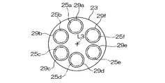
レボルバ部5は、回転軸線L3を中心に回転可能なレボルバ本体23と、レボルバ本体23に取り付けられた倍率の異なる複数の対物レンズ25とを備えている。レボルバ本体23は、レボルバ駆動手段(対物レンズ切換手段)27により回転軸線L3を中心に回転させて任意の対物レンズ25を観察光路内に挿入するように構成されている。なお、レボルバ駆動手段27は、例えば、電動モータから構成されている。このレボルバ本体23には、図2に示すように、回転軸線L3回りに各対物レンズ25を着脱可能に取り付ける複数(図示例では6つ)の取付部29a〜29fが均等に設けられている。
The revolver unit 5 includes a
複数の対物レンズ25は、これらレボルバ本体23の取付部29a〜29fにそれぞれ1つずつ装着されている。すなわち、最低倍率である可視光線用の対物レンズ25a(以下、可視光対物レンズ25aと呼ぶ)が取付部29aに装着され、回転軸線L3を中心として半時計回りに順次倍率が高くなる可視光対物レンズ25b〜25eが取付部29b〜29eに装着されている。また、2つの取付部29a,29eの間に配された取付部29fには、紫外線用の対物レンズ25f(以下紫外光対物レンズ25fと呼ぶ)が装着されている。なお、一般に倍率が高い程WDが短くなり、紫外光対物レンズ25fは、いずれの可視光対物レンズ25a〜25eの倍率よりも高いため、そのWD(半導体ウエハSとの隙間)が最も小さくなる。これら各取付部29a〜29fと対物レンズ25の倍率や種類とを対応づけたデータは、後述する制御PCのメモリ部に予め記憶されている。
このレボルバ部5には、図1に示すように、対物レンズ検出手段31が接続されており、どの取付部29a〜29fが観察光路内に配されているかを検出するように構成されている。そして、この対物レンズ検出手段31は、上述の検出結果とメモリ部に記憶されたデータとに基づいて、観察光路内に挿入された対物レンズ25の倍率・種類を検出するように構成されている。
The plurality of
As shown in FIG. 1, the revolver unit 5 is connected to an objective
また、この検査装置1は、試料ステージ部3、キューブ切換手段19及びレボルバ駆動手段27の動作を制御する制御PC33と、制御PC33、キューブ切換手段19、キューブ検出手段21、レボルバ駆動手段27及び対物レンズ検出手段31の間で、相互に情報のやりとりを行うためのCPU制御手段35とを備えている。そして、制御PC33は、モニタ37、操作部39及びメモリ部41を備えている。
モニタ37は、半導体ウエハSに関する各種情報を表示するものである。すなわち、モニタ37の画面上には、図3に示すように、前述したCCDカメラにおいて取得した半導体ウエハSの観察領域の画像を表示するメイン画面37bと、メイン画面37bがどの回路パターンを表示しているかを表示するウエハマップ37dと、メイン画面37bが回路パターン内のどの位置を表示しているかを表示するショットマップ37eとが表示されている。また、この画面上には、回路単位やステップ単位若しくは連続的に吸着プレート9をX軸方向及びY軸方向に移動させるための8方向移動ボタン37fや、メイン画面37bの倍率、座標等の各種情報表示や、検査結果や倍率、座標を変更するための各種操作ボタンを表示する情報表示領域37gが表示されている。また、8方向移動ボタン37fの操作によって吸着プレート9を移動させる速度モードの切り換えを行うための移動速度モード切換ボタン38も表示されている。
In addition, the
The
操作部39は、検査装置1の操作者が各種情報を入力するためのキーボード、吸着プレート9をX軸方向及びY軸方向に移動させるためのジョグハンドルノブ、及びモニタ37の画面の任意位置をクリックして各種情報を入力するマウス(いずれも図示せず)を備えている。
キーボードにおいて入力する情報には、観察に使用する光源の切り換え及びフィルターキューブの切り換え、観察光路内に挿入する対物レンズ25の切り換え等の切換情報がある。したがって、例えば、フィルターキューブの切換情報を入力した際には、この切換情報及びキューブ検出手段21からの検出結果に基づいてキューブ切換手段19が観察光路に配するフィルターキューブを変更する。また、例えば、対物レンズ25の切り換え情報を入力した際には、この切換情報及び対物レンズ検出手段31からの検出結果に基づいてレボルバ駆動手段27が観察光路内に挿入する対物レンズ25を切り換える。
また、キーボードにより光源又はフィルターキューブのいずれか一方の切換情報を入力した際には、この切換情報の内容に合致するように、光源、フィルターキューブ、対物レンズ25の他の切り換えが連動して行われる。すなわち、例えば、観察に使用する光源を可視光線から紫外線に切り換える情報を入力した際には、この切り換えと同時に、紫外光観察用キューブが観察光路内に配され、紫外光対物レンズ25fが挿入される。
The
Information input on the keyboard includes switching information such as switching of the light source used for observation, switching of the filter cube, switching of the
In addition, when switching information of either the light source or the filter cube is input from the keyboard, other switching of the light source, the filter cube, and the
ジョグハンドルノブを操作した際には、その操作方向に応じて制御PC33からXステージ13及びYステージ15に、吸着プレート9をX軸方向及びY軸方向に移動させる情報が出力される。この際には、モニタ37に表示される画像の観察領域が、ジョグハンドルノブの操作方向に移動することになる。なお、ジョグハンドルノブの操作による吸着プレート9の移動は、高速モード及び低速モードの2種類の移動速度で行うことができ、キーボードのキー操作により2つのモードのいずれかに切り換えることができる。この速度モードの切り換えは、例えば、モニタ37の画面に表示されるポインタ37aを移動速度モード切換ボタン38上に配して、クリックすることで実行される。
When the jog handle knob is operated, information for moving the
マウスにおいては、例えば、キーボードの代わりに、モニタ37の画面に表示される各種ボタンをクリックして各種情報を入力することができる。また、例えば、ジョグハンドルノブの代わりに吸着プレート9を移動させることができる。すなわち、図3(a)に示すように、モニタ37の画面に表示されるポインタ37aを半導体ウエハの観察領域37b中の所望位置に配してクリック動作を行うことにより、図3(b)に示すように、前述の所望位置がメイン画面37bの中心37cに位置するように、吸着プレート9が移動することになる。また、ポインタ37aをウエハマップ37d、ショットマップ37e上の所定位置に配してクリック動作を行うことでも、同様に吸着プレート9を移動させることができる。さらに、ポインタ37aを8方向移動ボタン37f上の所定位置に配してクリック動作を行うことでも、吸着プレート9を移動させることができる。なお、このマウスのクリック動作による吸着プレート9の移動は、その移動距離、倍率等により予め設定された速度のモードで行われる。
In the mouse, for example, various types of information can be input by clicking various buttons displayed on the screen of the
また、この検査装置1において、半導体ウエハS上の欠陥の位置座標が予め分かっている場合には、観察領域を半導体ウエハSの表面Saに点在する欠陥を順次モニタ37のメイン画面37bに表示するように、複数の欠陥の間で吸着プレート9を移動させるスキャン動作ができるようになっている。このスキャン動作は、操作部39において所定の操作を行うことにより実行される。なお、このスキャン動作に伴う吸着プレート9の移動は高速モードで行われる。また、スキャン動作における吸着プレート9の移動範囲は、半導体ウエハSの表面Sa全体となっている。
In the
メモリ部(移動制御手段)41には、高い倍率でWDが短く、半導体ウエハSとの干渉の発生の虞のある紫外光対物レンズ25fが観察光路内に挿入された状態において、X軸方向及びY軸方向に関する吸着プレート9の移動を規制する規制情報が記憶されている。この規制情報には、スキャン動作の禁止、移動範囲の限定、移動速度の限定がある。
移動範囲の限定とは、観察光路内に挿入する対物レンズを紫外光対物レンズ25fに切り換えた際にモニタ37の画面に表示される観察領域37bの中心37cの位置を基準として、操作部39の操作による吸着プレート9の移動範囲を観察領域の約10倍に限定することを示している。また、移動速度の限定とは、ジョグハンドルノブや8方向移動ボタン37fの操作による吸着プレート9の移動を低速モードでの移動のみに限定することを示している、すなわち、キーボードのキー操作や移動速度モード切換ボタン38による2つの速度モードの切り換えができないことを示している。
そして、紫外光対物レンズ25fが観察光路内に挿入された状態においては、制御PC33が、メモリ部41の規制情報に基づいて吸着プレート9の移動を規制する移動制御手段として機能する。
In the memory unit (movement control means) 41, in a state where the ultraviolet light
The movement range is limited based on the position of the
In a state where the ultraviolet light
なお、この検査装置1においては、レボルバ駆動手段27により対物レンズ25の切り換えを行う前に、Zステージ11により半導体ウエハSを対物レンズ25から離すようにZ軸方向に吸着プレート9を移動させて、対物レンズ25と半導体ウエハSとが接触することを防止している。
また、この検査装置1においては、観察光路内に挿入する対物レンズ25の切り換えを行った後に、対物レンズ25と半導体ウエハSの表面Saとの隙間が挿入した対物レンズ25のWD(作動距離)に等しくなるように、Zステージ11により吸着プレート9を光軸L1方向に移動させるオートフォーカス(AF)動作を行うようになっている。
なお、具体的なAF動作は、可視光対物レンズ25a〜25eを用いる場合と紫外光対物レンズ25fを用いる場合とで異なる。すなわち、可視光対物レンズ25a〜25eを用いる場合のピント合わせは、周知のナイフエッジ法などで自動的に行う。
また、紫外光対物レンズ25fのWDは予め分かっている。このため、紫外光対物レンズを用いる場合のピント合わせは、予め可視光対物レンズ25a〜25eを用いて合焦させた後に、この合焦位置を基準として、紫外光対物レンズ25fと半導体ウエハSの表面Saとの隙間が紫外光対物レンズ25fのWDと等しくなるように、吸着プレート9を自動的に移動させて行う。
In this
In this
A specific AF operation is different between the case where the visible light
The WD of the ultraviolet
次に、上記のように構成された検査装置1の動作について説明する。
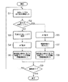
半導体ウエハSの表面Saに存在する欠陥の拡大観察を行う際には、はじめに、観察する半導体ウエハSを吸着プレート9に載置し、半導体ウエハSの裏面Sbを吸着プレート9に吸着させる。次いで、図4に示すように、操作部39において所定の対物レンズ25に切り換える指示を入力する(ステップS1)。この際には、レボルバ駆動手段27がレボルバ本体23を回転させて、所定の対物レンズ25を観察光路内に挿入する。そして、制御PC33は、対物レンズ検出手段31の検出結果に基づいて所定の対物レンズ25の種類を認識し、所定の対物レンズ25が紫外光対物レンズ25fであるか否かを判別する(ステップS2)。
Next, the operation of the
When performing magnified observation of defects existing on the surface Sa of the semiconductor wafer S, first, the semiconductor wafer S to be observed is placed on the
ここで、所定の対物レンズ25が可視光対物レンズ25a〜25eである場合には、制御PC33が、所定の可視光対物レンズ25a〜25eの種類を確認し(ステップS3)、可視光対物レンズ25a〜25eのWDに合わせて、AF機構により合焦位置を算出し、Zステージ11により吸着プレート9をZ軸方向に移動させてAF動作(ピント合わせ工程)を行う(ステップS4)。その後、操作部39を操作して、吸着プレート9をX軸方向及びY軸方向に移動させる観察位置移動工程を行い(ステップS5)、観察領域を半導体ウエハSの欠陥位置に移動させて欠陥の拡大観察を行う。なお、ステップS5における吸着プレート9の移動は、低速モード及び高速モードの2種類の移動速度で行うことができ、吸着プレート9の移動範囲も限定されない。また、ステップS5においてはスキャン動作も可能となっている。
Here, when the predetermined
また、ステップS2において、所定の対物レンズ25が紫外光対物レンズ25fであることを制御PC33が認識した場合には、ステップS4と同様に、可視光用対物レンズのAF動作時の値をもとに、半導体ウエハSを紫外光対物レンズ25fの焦点に合わせるAF動作(ピント合わせ工程)を行い(ステップS6)、メモリ部41から規制情報が読み出される(ステップS7)。その後、操作部39を操作して、吸着プレート9をX軸方向及びY軸方向に移動させる観察位置移動工程を行い(ステップS8)、観察領域を半導体ウエハSの欠陥位置に移動させて欠陥の拡大観察を行う。
このステップS8における吸着プレート9の移動は、前述の規制情報に基づいて規制される。すなわち、ジョイスティックや8方向移動ボタン37fの操作による吸着プレート9の移動が、低速モードでの移動のみに限定される。また、ジョグハンドルノブ及びマウスの操作による吸着プレート9の移動範囲が、観察領域の約10倍に限定され、スキャン動作も禁止される。
なお、ステップS5及びステップS8における吸着プレート9の移動は、ステップS1の情報入力を再度行うまで、若しくは、半導体ウエハSの欠陥の観察を終了する(ステップS9)まで行うことができる。
In step S2, if the
The movement of the
Note that the movement of the
上記のように、この検査装置1によれば、可視光対物レンズ25a〜25eよりもWD(作動距離)が小さい高倍率の紫外光対物レンズ25fを選択して半導体ウエハSの拡大観察を行う場合には、X軸方向及びY軸方向に関して紫外光対物レンズ25fと吸着プレート9の移動範囲及び移動速度が規制されるため、吸着プレート9に載置した半導体ウエハSの反りや撓みに基づいて紫外光対物レンズ25fと半導体ウエハSとが接触することを回避できる。
また、紫外光対物レンズ25fと半導体ウエハSとの接触を防止するために、紫外光対物レンズ25fと半導体ウエハSとの距離を測定する距離センサや、半導体ウエハSの反り・撓みを矯正する全面吸着プレート等を新たに設ける必要が無いため、検査装置1の製造コストの削減を図ることができる。
As described above, according to the
In addition, in order to prevent contact between the ultraviolet light
なお、上記の実施の形態においては、紫外光対物レンズ25fが観察光路内に配された場合に、メモリ部に記憶された規制情報に基づいて吸着プレート9の移動範囲及び移動速度を限定するとしたが、これに限ることはなく、例えば、Xステージ13及びYステージ15による吸着プレート9の移動を禁止するとしても構わない。この構成の場合には、紫外光対物レンズ25fを選択して半導体ウエハSの拡大観察を行う際に、紫外光対物レンズ25fと半導体ウエハSとの接触を確実に防止できる。
また、吸着プレート9の移動規制は、紫外光対物レンズ25fが観察光路内に配された場合に限ることはなく、少なくとも半導体ウエハSの反りや撓みの大きさよりも小さなWD(作動距離)の対物レンズを選択した場合に行われればよい。すなわち、例えば、半導体ウエハSの反りや撓みが最高倍率の可視光対物レンズ25eのWD(作動距離)よりも大きい場合には、紫外光対物レンズ25fに加えてWDが短く、干渉の虞のあるの可視光対物レンズ25eを選択した際にも、吸着プレート9の移動規制が行われることが好ましい。
In the above embodiment, when the ultraviolet
Further, the movement restriction of the
さらに、AF動作により半導体ウエハSの表面Saを対物レンズ25の焦点位置に合わせるとしたが、これに限ることはなく、例えば、操作部39の操作に基づいてZステージ11による吸着プレート9の光軸と平行な方向への移動(マニュアルフォーカス動作)を行い、半導体ウエハSの表面Saを対物レンズ25の焦点位置に合わせるとしてもよい。
また、試料ステージ部3が吸着プレート9をZ軸方向に移動させるZステージ11を備えるとしたが、これに限ることはなく、少なくともZ軸方向に関して対物レンズ25と吸着プレート9との相対的な移動が可能であればよい。すなわち、試料ステージ部3にZステージ11を設けずに、例えば、図5に示すように、レボルバ部5を光軸L1方向に移動させるZステージ12を設けるとしても構わない。この構成においては、レボルバ部5の光軸L1方向の位置情報やレボルバ部5を移動させる情報等、Zステージ12と制御PC33との間でやりとりされる各種情報の伝達がCPU制御手段を介して行われる。
Further, although the surface Sa of the semiconductor wafer S is adjusted to the focal position of the
In addition, the sample stage unit 3 includes the
以上、本発明の実施形態について図面を参照して詳述したが、具体的な構成はこの実施形態に限られるものではなく、本発明の要旨を逸脱しない範囲の設計変更等も含まれる。 As mentioned above, although embodiment of this invention was explained in full detail with reference to drawings, the concrete structure is not restricted to this embodiment, The design change etc. of the range which does not deviate from the summary of this invention are included.
1 検査装置(観察装置)
9 吸着プレート(載置ステージ)
11,12 Zステージ(移動手段)
13 Xステージ(移動手段)
15 Yステージ(移動手段)
23 レボルバ本体
25 対物レンズ
27 レボルバ駆動手段(対物レンズ切換手段)
31 対物レンズ検出手段
33 制御PC(移動制御手段)
S 半導体ウエハ(基板)
Sa 表面
1 Inspection device (observation device)
9 Suction plate (mounting stage)
11, 12 Z stage (moving means)
13 X stage (moving means)
15 Y stage (moving means)
23
31 Objective lens detection means 33 Control PC (movement control means)
S Semiconductor wafer (substrate)
Sa surface
Claims (5)
倍率の異なる複数の対物レンズを装着したレボルバと、
前記レボルバを動作させて観察光路内に挿入する前記対物レンズを切り換える対物レンズ切換手段と、
前記観察光路内に挿入された前記対物レンズに対向して設けられ、前記基板の表面が前記観察光路の光軸に略直交するように前記基板を載置する載置ステージと、
前記観察光路内に挿入された前記対物レンズの倍率を検出する対物レンズ検出手段と、
前記観察光路の光軸方向及び該光軸の直交方向に前記対物レンズと前記載置ステージとを相対的に移動させる移動手段と、
前記レンズ検出手段が所定倍率よりも高い倍率の対物レンズを検出した際に、前記直交方向に関して前記移動手段による前記対物レンズと前記載置ステージとの相対移動を規制する移動制御手段とを備えることを特徴とする観察装置。 An observation device that performs observation by magnifying the surface of a substrate using an objective lens,
A revolver equipped with a plurality of objective lenses with different magnifications;
Objective lens switching means for switching the objective lens to be operated and inserted into the observation optical path by operating the revolver;
A mounting stage provided facing the objective lens inserted in the observation optical path, and mounting the substrate so that the surface of the substrate is substantially orthogonal to the optical axis of the observation optical path;
Objective lens detection means for detecting the magnification of the objective lens inserted in the observation optical path;
Moving means for relatively moving the objective lens and the mounting stage in the optical axis direction of the observation optical path and the orthogonal direction of the optical axis;
And a movement control means for restricting relative movement between the objective lens and the mounting stage by the moving means in the orthogonal direction when the lens detecting means detects an objective lens having a magnification higher than a predetermined magnification. An observation apparatus characterized by.
前記基板の表面を前記対物レンズの焦点位置に配するように、前記基板の表面に略直交する前記対物レンズの光軸方向に前記対物レンズと前記基板とを相対的に移動させるピント合わせ工程と、
前記光軸の直交方向に前記対物レンズと前記基板とを相対的に移動させて、前記基板表面の拡大観察位置を変更する観察位置移動工程とを備え、
所定倍率よりも高い倍率の前記対物レンズを用いて前記基板の拡大観察を行う際に、前記観察位置移動工程における前記対物レンズと前記基板との相対的な移動を規制することを特徴とする基板の観察方法。
A method for observing a substrate for appropriately observing a surface of a substrate by appropriately selecting a plurality of objective lenses having different magnifications,
A focusing step of relatively moving the objective lens and the substrate in an optical axis direction of the objective lens substantially orthogonal to the surface of the objective lens so as to place the surface of the substrate at a focal position of the objective lens; ,
An observation position moving step of changing the magnification observation position of the substrate surface by relatively moving the objective lens and the substrate in a direction orthogonal to the optical axis,
A substrate that restricts relative movement between the objective lens and the substrate in the observation position moving step when performing magnification observation of the substrate using the objective lens having a magnification higher than a predetermined magnification. Observation method.
Priority Applications (5)
| Application Number | Priority Date | Filing Date | Title |
|---|---|---|---|
| JP2004076267A JP2005266083A (en) | 2004-03-17 | 2004-03-17 | Device and method for observation |
| US11/078,084 US7456947B2 (en) | 2004-03-17 | 2005-03-11 | Inspecting apparatus and inspecting method |
| KR1020050020940A KR20060044352A (en) | 2004-03-17 | 2005-03-14 | Inspecting apparatus and inspecting method |
| TW094107689A TWI364552B (en) | 2004-03-17 | 2005-03-14 | Inspecting apparatus and inspecting method |
| CNA2005100558536A CN1670940A (en) | 2004-03-17 | 2005-03-15 | Inspecting apparatus and inspecting method |
Applications Claiming Priority (1)
| Application Number | Priority Date | Filing Date | Title |
|---|---|---|---|
| JP2004076267A JP2005266083A (en) | 2004-03-17 | 2004-03-17 | Device and method for observation |
Publications (2)
| Publication Number | Publication Date |
|---|---|
| JP2005266083A true JP2005266083A (en) | 2005-09-29 |
| JP2005266083A5 JP2005266083A5 (en) | 2007-04-26 |
Family
ID=34985878
Family Applications (1)
| Application Number | Title | Priority Date | Filing Date |
|---|---|---|---|
| JP2004076267A Pending JP2005266083A (en) | 2004-03-17 | 2004-03-17 | Device and method for observation |
Country Status (5)
| Country | Link |
|---|---|
| US (1) | US7456947B2 (en) |
| JP (1) | JP2005266083A (en) |
| KR (1) | KR20060044352A (en) |
| CN (1) | CN1670940A (en) |
| TW (1) | TWI364552B (en) |
Cited By (5)
| Publication number | Priority date | Publication date | Assignee | Title |
|---|---|---|---|---|
| JP2007047080A (en) * | 2005-08-11 | 2007-02-22 | Hitachi High-Technologies Corp | Scanning electron microscope and its image display method |
| JP2010169892A (en) * | 2009-01-22 | 2010-08-05 | Olympus Corp | Microscope system |
| CN103984361A (en) * | 2013-02-07 | 2014-08-13 | 索尼公司 | Image obtaining apparatus and stage control method |
| JP2015069202A (en) * | 2013-10-01 | 2015-04-13 | オリンパス株式会社 | Microscope system |
| WO2021199340A1 (en) * | 2020-03-31 | 2021-10-07 | 株式会社日立ハイテク | Defect inspection device and defect inspection method |
Families Citing this family (10)
| Publication number | Priority date | Publication date | Assignee | Title |
|---|---|---|---|---|
| JP4933057B2 (en) * | 2005-05-13 | 2012-05-16 | キヤノン株式会社 | Head substrate, recording head, and recording apparatus |
| US20080243299A1 (en) * | 2007-03-27 | 2008-10-02 | Haas Automation, Inc. | Machine tool control system |
| US7812971B2 (en) * | 2007-06-28 | 2010-10-12 | Quality Vision International, Inc. | Multi color autofocus apparatus and method |
| KR100837729B1 (en) * | 2007-10-09 | 2008-06-13 | 서울엔지니어링(주) | Stage precision liner motion device for lcd inspection equipment |
| JP5555014B2 (en) * | 2010-03-10 | 2014-07-23 | オリンパス株式会社 | Virtual slide creation device |
| JP2012225701A (en) * | 2011-04-18 | 2012-11-15 | Mitsutoyo Corp | Shape measuring device |
| US9182341B2 (en) * | 2012-06-13 | 2015-11-10 | Kla-Tencor Corporation | Optical surface scanning systems and methods |
| US20140135581A1 (en) * | 2012-11-14 | 2014-05-15 | Gynius Ab | Portable battery powered self-illuminated multispectral multi-magnification colposcope |
| US9304089B2 (en) * | 2013-04-05 | 2016-04-05 | Mitutoyo Corporation | System and method for obtaining images with offset utilized for enhanced edge resolution |
| CN113433134A (en) * | 2021-06-24 | 2021-09-24 | 深圳中科飞测科技股份有限公司 | Detection method, detection device and computer-readable storage medium |
Citations (8)
| Publication number | Priority date | Publication date | Assignee | Title |
|---|---|---|---|---|
| JPS5793311A (en) * | 1980-12-02 | 1982-06-10 | Olympus Optical Co Ltd | Controller for relative moving speed of mirror body and sample in microscope |
| JPS62102752A (en) * | 1985-10-31 | 1987-05-13 | オリンパス光学工業株式会社 | Microscope moving apparatus |
| JPH07168101A (en) * | 1993-12-15 | 1995-07-04 | Olympus Optical Co Ltd | Microscope device |
| JPH09127426A (en) * | 1995-10-31 | 1997-05-16 | Nikon Corp | Driving commander for macroobservation apparatus |
| JP2000075215A (en) * | 1998-08-27 | 2000-03-14 | Nikon Corp | Microscope with motor driven stage |
| JP2001134760A (en) * | 1999-11-02 | 2001-05-18 | Sony Corp | Focal position control mechanism and examination device for ultraviolet light |
| JP2001201694A (en) * | 2000-01-18 | 2001-07-27 | Olympus Optical Co Ltd | Microscopic device |
| JP2002328306A (en) * | 2001-04-27 | 2002-11-15 | Nikon Corp | Ultraviolet microscope and observation method using the same |
Family Cites Families (17)
| Publication number | Priority date | Publication date | Assignee | Title |
|---|---|---|---|---|
| US3565512A (en) * | 1969-04-29 | 1971-02-23 | Bausch & Lomb | Microscope nosepiece assembly having adjustable optical components |
| DE2102922C3 (en) * | 1971-01-22 | 1978-08-24 | Ernst Leitz Wetzlar Gmbh, 6330 Wetzlar | Arrangement for automatic focusing on objects to be viewed in optical devices |
| US4503555A (en) * | 1982-04-21 | 1985-03-05 | University Of California | Semi-automatic optical scanning apparatus utilizing line integration |
| US4577141A (en) * | 1983-11-30 | 1986-03-18 | Nippon Kogaku K.K. | System for driving a movable stage |
| US4725720A (en) * | 1985-05-27 | 1988-02-16 | Mitutoyo Manufacturing Co., Ltd. | Microscope with auto focus and light adjusting means |
| US4695137A (en) * | 1986-02-26 | 1987-09-22 | Carl-Zeiss-Stiftung, Heidenheim/Brenz | Motorized focus drive for a microscope |
| EP0311096B1 (en) * | 1987-10-09 | 1993-03-24 | Olympus Optical Co., Ltd. | Coarse/fine adjustment coaxial handle for feeding microscope stage |
| CA1308203C (en) * | 1989-06-01 | 1992-09-29 | Nanoquest (Canada) Inc. | Magnification compensation apparatus |
| JP2925647B2 (en) * | 1990-04-16 | 1999-07-28 | オリンパス光学工業株式会社 | Microscope magnification changer |
| US5557456A (en) * | 1994-03-04 | 1996-09-17 | Oncometrics Imaging Corp. | Personal interface device for positioning of a microscope stage |
| US5818637A (en) * | 1996-02-26 | 1998-10-06 | Hoover; Rex A. | Computerized video microscopy system |
| US6248988B1 (en) * | 1998-05-05 | 2001-06-19 | Kla-Tencor Corporation | Conventional and confocal multi-spot scanning optical microscope |
| JP2001332595A (en) | 2000-05-25 | 2001-11-30 | Sony Corp | Focus control mechanism and inspection apparatus using the same |
| US6906858B2 (en) * | 2000-07-17 | 2005-06-14 | Olympus Optical Co., Ltd. | Microscope provided with an objective lens focusing apparatus and an objective lens switching apparatus |
| JP4121735B2 (en) * | 2001-01-22 | 2008-07-23 | ソニー株式会社 | Polysilicon film evaluation system |
| DE10159239A1 (en) * | 2001-12-03 | 2003-06-26 | Leica Microsystems | Microscope objective, microscope and method for imaging a sample |
| US6989927B2 (en) * | 2003-07-02 | 2006-01-24 | Leica Microsystems Inc. | Stage well |
-
2004
- 2004-03-17 JP JP2004076267A patent/JP2005266083A/en active Pending
-
2005
- 2005-03-11 US US11/078,084 patent/US7456947B2/en not_active Expired - Fee Related
- 2005-03-14 TW TW094107689A patent/TWI364552B/en not_active IP Right Cessation
- 2005-03-14 KR KR1020050020940A patent/KR20060044352A/en not_active Application Discontinuation
- 2005-03-15 CN CNA2005100558536A patent/CN1670940A/en active Pending
Patent Citations (8)
| Publication number | Priority date | Publication date | Assignee | Title |
|---|---|---|---|---|
| JPS5793311A (en) * | 1980-12-02 | 1982-06-10 | Olympus Optical Co Ltd | Controller for relative moving speed of mirror body and sample in microscope |
| JPS62102752A (en) * | 1985-10-31 | 1987-05-13 | オリンパス光学工業株式会社 | Microscope moving apparatus |
| JPH07168101A (en) * | 1993-12-15 | 1995-07-04 | Olympus Optical Co Ltd | Microscope device |
| JPH09127426A (en) * | 1995-10-31 | 1997-05-16 | Nikon Corp | Driving commander for macroobservation apparatus |
| JP2000075215A (en) * | 1998-08-27 | 2000-03-14 | Nikon Corp | Microscope with motor driven stage |
| JP2001134760A (en) * | 1999-11-02 | 2001-05-18 | Sony Corp | Focal position control mechanism and examination device for ultraviolet light |
| JP2001201694A (en) * | 2000-01-18 | 2001-07-27 | Olympus Optical Co Ltd | Microscopic device |
| JP2002328306A (en) * | 2001-04-27 | 2002-11-15 | Nikon Corp | Ultraviolet microscope and observation method using the same |
Cited By (6)
| Publication number | Priority date | Publication date | Assignee | Title |
|---|---|---|---|---|
| JP2007047080A (en) * | 2005-08-11 | 2007-02-22 | Hitachi High-Technologies Corp | Scanning electron microscope and its image display method |
| JP4644065B2 (en) * | 2005-08-11 | 2011-03-02 | 株式会社日立ハイテクノロジーズ | Scanning electron microscope and image display method thereof |
| JP2010169892A (en) * | 2009-01-22 | 2010-08-05 | Olympus Corp | Microscope system |
| CN103984361A (en) * | 2013-02-07 | 2014-08-13 | 索尼公司 | Image obtaining apparatus and stage control method |
| JP2015069202A (en) * | 2013-10-01 | 2015-04-13 | オリンパス株式会社 | Microscope system |
| WO2021199340A1 (en) * | 2020-03-31 | 2021-10-07 | 株式会社日立ハイテク | Defect inspection device and defect inspection method |
Also Published As
| Publication number | Publication date |
|---|---|
| KR20060044352A (en) | 2006-05-16 |
| CN1670940A (en) | 2005-09-21 |
| US20050206885A1 (en) | 2005-09-22 |
| TW200540455A (en) | 2005-12-16 |
| US7456947B2 (en) | 2008-11-25 |
| TWI364552B (en) | 2012-05-21 |
Similar Documents
| Publication | Publication Date | Title |
|---|---|---|
| US7456947B2 (en) | Inspecting apparatus and inspecting method | |
| CN101153852B (en) | Appearance detecting device | |
| KR100537684B1 (en) | Semiconductor wafer inspection system | |
| JP5525953B2 (en) | Dimension measuring apparatus, dimension measuring method and program for dimension measuring apparatus | |
| US20080079932A1 (en) | Visual inspection apparatus and visual inspection method | |
| JPH03296011A (en) | Magnification varying device for microscope | |
| KR20070053759A (en) | Fluorocope | |
| JP4567594B2 (en) | Microscope, sample observation method, and semiconductor inspection method | |
| JP2007234932A (en) | Device for checking external appearance | |
| JP2007059640A (en) | Visual inspection equipment | |
| JP2003015056A (en) | Method and device for picking up image | |
| JPH0735645A (en) | Apparatus for inspecting liquid crystal panel | |
| JP2007309718A (en) | Inspection device and method | |
| US6868354B2 (en) | Method of detecting a pattern and an apparatus thereof | |
| JP2004179581A (en) | Semiconductor wafer inspection device | |
| JP2001349848A (en) | Inspection apparatus and method | |
| JP2001343907A (en) | Laser repair device and production method for display cell | |
| JP2007033372A (en) | Visual inspection device | |
| JP2009052966A (en) | Substrate inspection device | |
| JP4477181B2 (en) | Microscope equipment | |
| JP4485771B2 (en) | Method of aligning rotation axis of chuck table and center of microscope in cutting apparatus | |
| JP2004264690A (en) | Misalignment correcting device and its method | |
| JP2011151165A (en) | Wafer inspection device, and wafer inspection method | |
| JP2009186414A (en) | Inspection microscope, microscope observation method, and microscopic observation program | |
| JP2004184411A (en) | Position recognition method |
Legal Events
| Date | Code | Title | Description |
|---|---|---|---|
| A521 | Request for written amendment filed |
Free format text: JAPANESE INTERMEDIATE CODE: A523 Effective date: 20070307 |
|
| A621 | Written request for application examination |
Free format text: JAPANESE INTERMEDIATE CODE: A621 Effective date: 20070307 |
|
| A977 | Report on retrieval |
Free format text: JAPANESE INTERMEDIATE CODE: A971007 Effective date: 20100421 |
|
| A131 | Notification of reasons for refusal |
Free format text: JAPANESE INTERMEDIATE CODE: A131 Effective date: 20100423 |
|
| A521 | Request for written amendment filed |
Free format text: JAPANESE INTERMEDIATE CODE: A523 Effective date: 20100622 |
|
| A521 | Request for written amendment filed |
Free format text: JAPANESE INTERMEDIATE CODE: A821 Effective date: 20100623 |
|
| A131 | Notification of reasons for refusal |
Free format text: JAPANESE INTERMEDIATE CODE: A131 Effective date: 20100727 |
|
| A02 | Decision of refusal |
Free format text: JAPANESE INTERMEDIATE CODE: A02 Effective date: 20101207 |