JP2005253166A - Power unit - Google Patents
Power unit Download PDFInfo
- Publication number
- JP2005253166A JP2005253166A JP2004058522A JP2004058522A JP2005253166A JP 2005253166 A JP2005253166 A JP 2005253166A JP 2004058522 A JP2004058522 A JP 2004058522A JP 2004058522 A JP2004058522 A JP 2004058522A JP 2005253166 A JP2005253166 A JP 2005253166A
- Authority
- JP
- Japan
- Prior art keywords
- power
- power supply
- load
- switch
- voltage
- Prior art date
- Legal status (The legal status is an assumption and is not a legal conclusion. Google has not performed a legal analysis and makes no representation as to the accuracy of the status listed.)
- Pending
Links
Images


Abstract
Description
本発明は電源装置に係り、特に微弱な発電電力を負荷に供給する電源装置に関する。 The present invention relates to a power supply device, and more particularly to a power supply device that supplies weak generated power to a load.
自然エネルギを利用した電源の従来例として、圧電素子を発信装置の電源として利用した自己発電型発信装置が知られている(例えば、特許文献1参照)。これは、圧電素子が発電した電力を容量に充電し、その電力を用いることにより比較的高い電力を要する発信動作を行うものである。その動作原理の概略は以下の通りである。 As a conventional example of a power source using natural energy, a self-powered transmitter using a piezoelectric element as a power source of the transmitter is known (see, for example, Patent Document 1). In this method, the power generated by the piezoelectric element is charged into a capacitor, and the power is used to perform a transmission operation that requires relatively high power. The outline of the operation principle is as follows.
容量の充電電圧を監視することにより、容量に信号を発信することができる電力を確保できたかどうかを判断し、確保できた場合は放電スイッチを介して電力を送信部に供給する。その後、発信終了時まで電力の供給は継続され、発信が終了すると効率よく電力を充電するために放電スイッチをオフし、電力の供給を停止するというものである。このような動作をする電源を構成することにより、圧電素子で発電された電力を効率よく活用して比較的高い電力を要する信号の発信をすることが可能となる。 By monitoring the charging voltage of the capacity, it is determined whether or not the power capable of transmitting a signal to the capacity has been secured, and when the power has been secured, the power is supplied to the transmitter via the discharge switch. Thereafter, the supply of power is continued until the end of the transmission, and when the transmission ends, the discharge switch is turned off to efficiently charge the power and the supply of power is stopped. By configuring a power supply that operates in this manner, it is possible to efficiently utilize the power generated by the piezoelectric element and transmit a signal that requires relatively high power.
前述した従来技術の電源装置は、圧電素子で発電された電力を用いて比較的高い電力を消費する負荷を駆動できる。しかしながら、この従来例の構成では電源の負荷である発信装置は、あらかじめ決められた動作をすることしか許されていない。なぜなら、この電源装置は、負荷が必要とするエネルギ確保の可否を容量の電圧が所定の電圧に達したかどうかで判断しているためである。従って、負荷は現時点で容量に存在するエネルギ量を知ることができないので、一度動作に必要なエネルギを確保した後に決まった動作を繰り返すことしかできず、センサネットシステムのような複雑な処理を行うシステムの電源装置としては使えない。 The above-described conventional power supply device can drive a load that consumes relatively high power using the power generated by the piezoelectric element. However, in the configuration of this conventional example, the transmitter that is the load of the power supply is only allowed to perform a predetermined operation. This is because this power supply device determines whether or not the energy required by the load can be secured by determining whether or not the voltage of the capacitor has reached a predetermined voltage. Therefore, since the load cannot know the amount of energy present in the capacity at the present time, it can only repeat the determined operation after securing the energy necessary for the operation once, and performs a complicated process like a sensor network system. Cannot be used as a system power supply.
また、発信部の動作中に誤動作や環境の変化などの原因で電力消費量が増加して充電エネルギが不足した場合、発信部の動作は突然停止するためシステムの信頼性が損なわれるという問題もある。さらにこの場合、負荷は放電スイッチをオフするための信号も出力しないので、放電スイッチはオンした状態で固定される。よって、エネルギの充電時にも無駄な電力を消費するため、容量の充電効率が悪くなるという問題もある。 In addition, if the power consumption increases due to malfunctions or environmental changes during the operation of the transmitter and the charging energy is insufficient, the operation of the transmitter stops suddenly and the reliability of the system is impaired. is there. Further, in this case, since the load does not output a signal for turning off the discharge switch, the discharge switch is fixed in an on state. Therefore, there is a problem that the capacity charging efficiency is deteriorated because useless power is consumed even when the energy is charged.
そこで、本発明の目的は、電力を蓄電容量に充電することにより、微弱な電源で大きな負荷を駆動できる信頼性の高い電源装置を提供することにある。 SUMMARY OF THE INVENTION An object of the present invention is to provide a highly reliable power supply device that can drive a large load with a weak power source by charging power to a storage capacity.
本発明の代表的手段の一例を示せば次の通りである。即ち、本発明に係る電源装置は、供給されるエネルギを充電する蓄電容量と、前記蓄電容量の充電電圧である第1及び第2の所定電圧に基づき前記蓄電容量に充電された充電エネルギの放電及び停止を制御する電力制御回路と、前記電力制御回路の制御により放電された前記充電エネルギを用いて所定の定電圧を負荷へ出力するレギュレータとを有し、
前記充電エネルギが前記第1の所定電圧以上の場合には、前記負荷を駆動するために前記充電エネルギの放電を可能とし、前記充電エネルギが前記第1の所定電圧よりも小さい前記第2の所定電圧以下の場合には、前記充電エネルギの前記負荷を駆動するための放電を停止することを特徴とするものである。
An example of representative means of the present invention is as follows. That is, the power supply device according to the present invention discharges the charging energy charged in the storage capacity based on the storage capacity for charging the supplied energy and the first and second predetermined voltages that are charging voltages of the storage capacity. And a power control circuit that controls the stop, and a regulator that outputs a predetermined constant voltage to a load using the charging energy discharged by the control of the power control circuit,
When the charging energy is equal to or higher than the first predetermined voltage, the charging energy can be discharged to drive the load, and the charging energy is smaller than the first predetermined voltage. When the voltage is equal to or lower than the voltage, discharging for driving the load of the charging energy is stopped.
この場合、上記の電源装置において、前記蓄電容量に供給されるエネルギは、自然エネルギを利用して発電する発電素子と、前記発電素子の出力と接地電位との間に直列にカソード同士を接続したダイオードとツェナダイオードとを含んでなる前記発電素子への逆流を防ぐ保護回路とを有する電源から供給されるようにすれば好適である。 In this case, in the above power supply device, the energy supplied to the power storage capacity includes a power generation element that generates power using natural energy, and cathodes connected in series between the output of the power generation element and the ground potential. It is preferable that power is supplied from a power source having a protection circuit that prevents backflow to the power generating element including a diode and a Zener diode.
本発明によれば、自然エネルギを利用して発電した微弱な電力が充電される蓄電容量の充電エネルギにより、大な負荷を駆動できる電源装置を実現できる。また、発電量が不安定でも信頼性の高い電源装置を実現できる。 ADVANTAGE OF THE INVENTION According to this invention, the power supply device which can drive a big load with the charge energy of the electrical storage capacity in which the weak electric power generated using natural energy is charged is realizable. In addition, a highly reliable power supply device can be realized even if the amount of power generation is unstable.
以下、本発明に係る電源装置の好適ないくつかの実施例について添付図面を参照しながら詳細に説明する。 Hereinafter, several preferred embodiments of a power supply device according to the present invention will be described in detail with reference to the accompanying drawings.
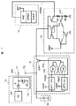
図1は、本発明に係る電源装置の第1の実施例の構成を示すブロック図であり、電源装置は、電源10と、蓄電容量SCと、電力制御回路12と、レギュレータ13とから構成され、負荷14を駆動する。ここで、電源10は、発電素子(GE)100と保護回路101で構成されている。発電素子100は、太陽、振動、温度差などの自然エネルギを利用して発電するものである。電源10の出力端子T1と電力制御回路の端子T2との間を接続することにより、蓄電容量SCに電源10で発電された電気エネルギが蓄積される。以下、電源10の出力端子T1と電力制御回路12の端子T2との間は、接続されているものとして説明する。
FIG. 1 is a block diagram showing a configuration of a first embodiment of a power supply apparatus according to the present invention. The power supply apparatus includes a
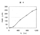
図8と図9に、発電素子として太陽電池と振動を用いた場合のそれぞれの発電量PWRを示す。太陽電池と振動を用いた発電素子の寸法はそれぞれ、53mm×50mm、50mm×30mmである。図8は太陽電池の発電量PWR[μW]の照度IL[Lx]依存性を、図9は振動を用いた発電素子の発電量PWR[μW]の振動振幅値AM[μm]依存性を示した図である。図8と図9から分かるように、このような自然エネルギを利用した発電素子の発電量は数百μW程度と微弱であり、また発電環境によって変動する。 FIG. 8 and FIG. 9 show the respective power generation amounts PWR when using solar cells and vibrations as power generation elements. The dimensions of the solar cell and the power generation element using vibration are 53 mm × 50 mm and 50 mm × 30 mm, respectively. FIG. 8 shows the illuminance IL [Lx] dependency of the power generation amount PWR [μW] of the solar cell, and FIG. 9 shows the dependency of the power generation amount PWR [μW] of the power generation element using vibration on the vibration amplitude value AM [μm]. It is a figure. As can be seen from FIGS. 8 and 9, the power generation amount of the power generation element using such natural energy is as weak as about several hundred μW, and varies depending on the power generation environment.
例えば、太陽電池であれば照度ILに応じて、振動であればその振幅値AMに応じて発電量が変動するという性質がある。 For example, the amount of power generation varies depending on the illuminance IL in the case of a solar cell and the amplitude value AM in the case of vibration.
保護回路101は、ダイオードDとツェナダイオードZDで構成される。発電素子100の出力は、ダイオードDを介して電源10の出力電圧VDCとして出力端子T1から外部へ出力されるため、外部からの電流の逆流を防止できる。また、保護回路101のツェナダイオードは出力電圧VDCと接地間に配置され、電圧VDCがツェナ電圧VLT以上になることを防止している。
The
蓄電容量SCは、電源10から供給される電力を、負荷14を動作させるための電力として蓄えておく容量である。電源10から蓄電容量SCに電力が供給されると出力電圧VDC、すなわち充電電圧VDCは上昇し、負荷14に対して充電エネルギを放電すれば充電電圧VDCは低下する。負荷14が消費する電力や充電電圧VDCの電圧にもよるが、蓄電容量SCとしては比較的容量が高く、等価抵抗の低いものが望ましい。
The storage capacity SC is a capacity for storing power supplied from the
電力制御回路12は、第1の所定電圧VHを監視する電圧監視回路DET1と、第1の所定電圧より低い第2の所定電圧VLを監視する電圧監視回路DET2と、電源スイッチSW1と、電圧監視回路DET1,2の出力VDECが入力される2個のNANDゲートN1,N2で構成されるスイッチ制御回路120とから構成される。
The
ここで、第2の所定電圧VLは負荷14を駆動するのに最低限必要な電圧値以上に設定される。電力制御回路12は、蓄電容量SCに充電された充電エネルギの放電を制御する回路である。蓄電容量SCとレギュレータ13との間に挿入された電源スイッチSW1は、スイッチであれば特に限定するものではないが、本実施例ではPMOSFETを用いている。このPMOSスイッチは、ゲートに印加されるスイッチ制御回路120の制御信号VCLが、ロー(“L”)の時にオンし、ハイ(“H”)の時にオフする。
Here, the second predetermined voltage VL is set to be equal to or higher than the minimum voltage value required to drive the
蓄電容量SCの充電電圧VDCを電圧監視回路DET1と電圧監視回路DET2で監視し、充電電圧VDCが第1の所定電圧VH以上に充電されると、スイッチ制御回路120は制御信号VCLを“L”レベルに制御し、蓄電容量SCに充電された充電エネルギを放電する。この後、充電電圧VDCが、第2の所定電圧VLに減少するまで放電は継続され、充電電圧VDCがVL以下になるとスイッチ制御回路120は制御信号VCLを“H”レベルに制御し、蓄電容量SCの放電を停止する。
The charging voltage VDC of the storage capacitor SC is monitored by the voltage monitoring circuit DET1 and the voltage monitoring circuit DET2, and when the charging voltage VDC is charged to be equal to or higher than the first predetermined voltage VH, the
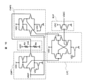
図10は、電圧監視回路DET1,DET2の構成の一例である。電圧監視回路DET1,DET2は同じ回路構成であり、検出する電圧値VHとVLを設定するための抵抗R3,R4の値が異なるだけであるので、電圧監視回路DET1について述べる。電圧監視回路DET1は、基準電圧VREFと抵抗R3とR4の接続ノードn34の電圧、すなわち充電電圧VDCを抵抗R3とR4で分割した電圧とを比較する2つの比較回路CMP1とCMP2、検出信号の振幅を充電電圧VDCレベルまで増幅するレベル変換回路LVCと、電圧監視回路が負荷の影響を受けないようにするためのCMOSインバータからなるバッファ回路BUFとで構成される。 FIG. 10 shows an example of the configuration of the voltage monitoring circuits DET1 and DET2. The voltage monitoring circuits DET1 and DET2 have the same circuit configuration, and only the values of resistors R3 and R4 for setting the voltage values VH and VL to be detected are different. Therefore, the voltage monitoring circuit DET1 will be described. The voltage monitoring circuit DET1 includes two comparison circuits CMP1 and CMP2 that compare the reference voltage VREF and the voltage of the connection node n34 of the resistors R3 and R4, that is, the voltage obtained by dividing the charging voltage VDC by the resistors R3 and R4, and the amplitude of the detection signal. Is converted to a charging voltage VDC level, and a buffer circuit BUF composed of a CMOS inverter for preventing the voltage monitoring circuit from being affected by the load.
このように構成される電圧監視回路DET1は、充電電圧VDCが(R3+R4)VREF/R4以上かどうかを判定する。したがって、第1の所定電圧VHを検出するためには充電電圧VDCの電圧値がVHとなったときにノードn34の電圧が基準電圧VREFと同じ電圧になるように、抵抗R3とR4の比を設定すればよい。 The voltage monitoring circuit DET1 configured as described above determines whether or not the charging voltage VDC is equal to or higher than (R3 + R4) VREF / R4. Therefore, in order to detect the first predetermined voltage VH, the ratio of the resistors R3 and R4 is set so that the voltage at the node n34 becomes the same voltage as the reference voltage VREF when the voltage value of the charging voltage VDC becomes VH. You only have to set it.
同様に、電圧監視回路DET2の場合は、第2の所定電圧VLを検出するように抵抗R3とR4の比を設定すればよい。 Similarly, in the case of the voltage monitoring circuit DET2, the ratio of the resistors R3 and R4 may be set so as to detect the second predetermined voltage VL.
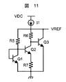
図11は基準電圧VREFを発生する基準電圧発生回路の一例を示す回路図である。電流源I1と、3個のNPNトランジスタQ1〜Q3と、3本の抵抗R5〜R7とから構成される公知のバンドギャップリファレンス回路であり、充電電圧VDCと接地間に挿入されて、定電圧VREFを出力する。なお、基準電圧発生回路は各回路の近傍にそれぞれ設けても良いし、配線抵抗により電圧降下が無視できる場合には1個の基準電圧発生回路から各回路へ基準電圧VREFを供給してもよい。 FIG. 11 is a circuit diagram showing an example of a reference voltage generating circuit that generates the reference voltage VREF. This is a known bandgap reference circuit composed of a current source I1, three NPN transistors Q1 to Q3, and three resistors R5 to R7, and is inserted between the charging voltage VDC and the ground so as to have a constant voltage VREF. Is output. The reference voltage generation circuit may be provided in the vicinity of each circuit, or when a voltage drop can be ignored due to wiring resistance, the reference voltage VREF may be supplied from one reference voltage generation circuit to each circuit. .
レギュレータ13は、基準電圧VREFを一方の入力とし、抵抗R1とR2の接続ノードn12の電圧を他方の入力として負帰還接続する非反転増幅回路で構成されるシリーズレギュレータである。非反転増幅回路は、基準電圧VREFを(R1+R2)/R2倍に増幅する。従って、レギュレータ13は出力電圧VREGとして、(R1+R2)VREF/R2を出力する。
The
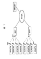
負荷14は、蓄電容量SCに充電された電力を消費する負荷である。本実施例では、図7に示すようなセンサネットシステムにおける無線(RAD)、マイクロプロセッサ(MPRO)、センサ(SENS)の各機能を備えたセンサネット端末を想定しているが、特にこれに限定するものではない。図7は、センサネットシステムの構成図である。センサネットシステムは、無数に存在する自律動作端末(SENSTM)が情報を検出し、基地局(BST)と通信することにより、その情報がネットワーク(NTWK)に直結され、処理が行われるというものである。センサネット端末はあらゆる場所に設置されるため電源の確保が課題である。そこで、微弱ではあるが自然エネルギを利用した電源が盛んに開発されている。
The
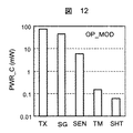
本実施例での負荷であるセンサネット端末14は情報をセンシングし、マイクロプロセッサにて処理し、基地局(BST)と情報を通信するものである。このセンサネット端末14は複数の動作モード(OP_MOD)を持っている。
The
図12はセンサネット端末14の動作モードと消費電力PWR_Cを示している。動作モードによって消費電力は大きく変動し、通信(TX)モード、信号処理(SG)、センシング(SEN)モード、等の幾つかの動作モードでは電源10が発電する電力よりも遥かに大きな電力を消費する。
FIG. 12 shows the operation mode and power consumption PWR_C of the
しかしながら、大部分の時間はタイマ動作(TM)モード、遮断(SHT)モードなどの低電力なモードで動作しており、極わずかな時間だけ信号処理や通信といった大きな電力を消費するモードで動作する。このようにセンサネット端末14は複数の動作モードを持ち、動作モードによって大きく消費電力が異なり、間欠的に大きな電力を消費するモードで動作することを特徴としている。
However, most of the time is operating in low-power modes such as timer operation (TM) mode and shut-off (SHT) mode, and it operates in a mode that consumes a large amount of power such as signal processing and communication for a very short time. . As described above, the
次に、本実施例の動作を説明する。
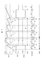
図2に、本実施例の蓄電容量SCの充電電圧VDC、スイッチ制御回路120の出力である制御信号VCL、レギュレータ13の出力電圧VREGの動作波形を示す。尚、図2において、横軸は時間であり、STは発電素子100による発電量PWRが強の場合、WKは発電量PWRが弱の場合を示している。また、PSSは電力供給源から電力が供給されている期間を示し、この場合は蓄電容量SCから充電エネルギが供給されている期間を示している。
Next, the operation of this embodiment will be described.
FIG. 2 shows operation waveforms of the charging voltage VDC of the storage capacitor SC, the control signal VCL that is the output of the
時刻Aで、電源10での発電が開始される。ここで、発電量PWRは強(ST)の状態である。蓄電容量SCが充電されるにつれて充電電圧VDCは上昇する。充電電圧VDCが第1の所定電圧VHに達するまでは、電力制御回路12内の電源スイッチSW1を制御する制御信号VCLは“H”となり、電源スイッチSW1はオフ状態であり、負荷14へは電力PWRは遮断されて供給されないので、動作モードOP_MODは遮断モードSHTである。
At time A, power generation by the
時刻Bで、充電電圧VDCが第1の所定電圧VHに達すると、制御信号VCLは“L”となり、電源スイッチSW1がオンして蓄電容量SCに充電されたエネルギが放電され、レギュレータ13は所定の定電圧VREGを負荷へ出力する。電力が供給されるとセンサネット端末14は、短時間だけ電力消費の大きなモードで動作する間欠動作を開始する。動作開始後、動作モードに応じて電力を消費し、それに伴い充電電圧VDCは低下していく。図2の例では、時刻B−C間で信号処理SGを、時刻C−D間で通信TXを行い、負荷14の消費電力に応じて充電電圧VDCが低下している。
When the charging voltage VDC reaches the first predetermined voltage VH at time B, the control signal VCL becomes “L”, the power switch SW1 is turned on, the energy charged in the storage capacitor SC is discharged, and the
時刻D以降、負荷14はタイマ動作TMに入る。タイマ動作は消費電力が小さいため、充電電圧VDCは回復していくが、保護回路101によりツェナ電圧VLT以上には上昇しない。
After time D, the
時刻G以降では、発電環境の変化により電源10の発電量PWRが低下し弱(WK)の状態である。そのため、負荷14が信号処理モードSGと通信モードTXの間欠的な動作を続けるに従って充電電圧VDCは徐々に低下していく。
After time G, the power generation amount PWR of the
時刻Pでは、遂に第2の所定電圧VLまで低下してしまう。充電電圧VDCがVL以下になると、再び制御信号VCLは“H”を出力して電源スイッチSW1をオフ状態にし、蓄電容量SCに充電されたエネルギの放電を停止する。一度、電源スイッチSW1がオフすると充電電圧VDCが再び第1の所定電圧VH以上に充電される時刻Qになるまで、オフ状態を継続し、電源10が発生する電力は充電にのみ充てられる。
At time P, the voltage finally drops to the second predetermined voltage VL. When the charging voltage VDC becomes equal to or lower than VL, the control signal VCL again outputs “H”, turns off the power switch SW1, and stops discharging the energy charged in the storage capacitor SC. Once the power switch SW1 is turned off, the off state is continued until the time Q at which the charging voltage VDC is charged to the first predetermined voltage VH or higher again, and the power generated by the
このように電源10で自然エネルギを用いて発電した電力を蓄電容量SCに充電し、充電電圧を第1の所定電圧VHと第2の所定電圧VLの2電圧で監視して蓄電容量SCの負荷14への放電をヒステリシス制御することにより、負荷回路の動作エネルギを効率よく十分に確保できる。従って、微弱な電源を用いて消費電力が過大な負荷を駆動できる電源装置が実現できる。
In this way, the power generated by the
本実施例では、例えば発電素子として太陽電池を、蓄電容量として22mF程度の容量を用いた場合に、蓄電容量の電圧は3.5〜5V程度に制御され、レギュレータの出力として3V程度の電圧を得ることができるので、5分毎に100msの期間、数10mWの電力を消費する間欠動作を行うようなセンサネットシステムのセンサネット端末用に好適な電源装置を提供できる。 In this embodiment, for example, when a solar cell is used as the power generation element and a capacity of about 22 mF is used as the storage capacity, the voltage of the storage capacity is controlled to about 3.5 to 5 V, and a voltage of about 3 V is used as the output of the regulator. Therefore, it is possible to provide a power supply device suitable for a sensor network terminal of a sensor network system that performs intermittent operation that consumes several tens of mW of power for a period of 100 ms every 5 minutes.
なお、図2では消費電力の大きい動作モードであるセンシング動作を省略して説明したが、センシングモード、信号処理モード、送信モードとを一組とした連続動作が間欠して動作を行う場合にも、同様に説明でき、その場合には消費電力が増えるので、間欠動作間隔が同じであれば、その分充電電圧VDCが第2の所定電圧VL以下になる時刻が早くなる。 In FIG. 2, the sensing operation, which is an operation mode with high power consumption, is omitted, but the case where the continuous operation with the sensing mode, the signal processing mode, and the transmission mode as a set is intermittently performed is also described. Since the power consumption increases in this case, if the intermittent operation interval is the same, the time at which the charging voltage VDC becomes equal to or lower than the second predetermined voltage VL is earlier.
図3は、本発明に係る電源装置の第2の実施例の構成を示すブロック図である。図3では電源と電力制御回路は端子が無く直接接続されているものとして図示してあるが、図1のように端子間を接続する構成としても良いことは勿論である。後述する図5の第3実施例においても同様である。 FIG. 3 is a block diagram showing the configuration of the second embodiment of the power supply apparatus according to the present invention. In FIG. 3, the power supply and the power control circuit are illustrated as being directly connected without terminals, but it is needless to say that the terminals may be connected as shown in FIG. The same applies to a third embodiment of FIG. 5 described later.
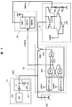
ここで、図1と対応する部分には同一参照符号を付し、その重複説明を省略する。すなわち、本実施例における電源装置は、蓄電容量SCに充電されたエネルギの放電を制御する電力制御回路32と負荷34を除いて、第1の実施例と同様の構成である。
Here, portions corresponding to those in FIG. 1 are denoted by the same reference numerals, and redundant description thereof is omitted. That is, the power supply apparatus in the present embodiment has the same configuration as that of the first embodiment except for the
電力制御回路32を構成する第2の所定電圧を監視する電圧監視回路DET2の検出電圧VL’は、負荷34を駆動するのに最低限必要な電圧VLよりも高い電圧である。
The detection voltage VL ′ of the voltage monitoring circuit DET2 that monitors the second predetermined voltage that constitutes the
スイッチ制御回路320は、実施例1のスイッチ制御回路120と異なり、NANDゲートN3と遅延回路Dが追加され、NANDゲートN3の出力により電源スイッチSW1を制御すると共に、NANDゲートN1の出力が蓄電電力の状態を示すVCHG信号として、センサネット端末である負荷34のマイクロプロセッサMPROへ送信される構成となっている。
Unlike the
VCHG信号は、“H”で充電エネルギが確保されているという状態を示し、“L”で充電エネルギが減少または枯渇しているという状態を示す。電力制御回路32は、蓄電容量SCの充電電圧VDCを電圧監視回路DET1とDET2で監視し、充電電圧VDCが第1の所定電圧VH以上に充電されると、スイッチ制御回路320はVCHG信号を“L”から“H”へ変化させ、蓄電容量SCに充電エネルギが十分に確保されたことを負荷34へ出力する。
The VCHG signal indicates a state where charging energy is secured at “H”, and indicates a state where charging energy is reduced or exhausted at “L”. The
また、制御信号VCLを“H”から“L”へ変化させることで電源スイッチSW1をオンさせて蓄電容量SCに蓄電された充電エネルギを放電する。引き続き放電は継続され、充電電圧VDCが第2の所定電圧VL’にまで減少するとVCHG信号を“L”に制御し、負荷34へ蓄電電力が減少したことを示す警告信号を送る。そして、スイッチ制御回路320内の遅延回路Dで設定された時間後、制御信号VCLを“H”に制御して蓄電容量SCの充電エネルギの放電を停止する。遅延回路Dの遅延時間は、警告信号送信後に負荷34で行われる終了処理に要する以上の時間に設定される。
Further, by changing the control signal VCL from “H” to “L”, the power switch SW1 is turned on to discharge the charging energy stored in the storage capacitor SC. The discharge continues, and when the charging voltage VDC decreases to the second predetermined voltage VL ′, the VCHG signal is controlled to “L”, and a warning signal indicating that the stored power has decreased is sent to the
負荷34は、第1の実施例と同じ構成の負荷にVCHG信号を入力として追加したものである。負荷34は、VCHG信号が“H”の場合、蓄電容量SCの充電エネルギが供給され、通信や信号処理などの動作を間欠的に行う。蓄電容量SCに充電されたエネルギが減少し、“L”レベルのVCHG信号が入力されると、負荷34は動作モードを変更し、あらかじめ決められた動作を終了動作として行う。また、基地局へ停止信号を送信し、ネットワークシステムの安定度を増すこともできる。これらの動作を終えると電源が遮断されるのを待つ。
The
なお、遅延回路Dとしては、例えばインバータを縦列接続した構成の遅延回路を用いることができるが、これに限るものではなく、他の構成の遅延回路を用いても良い。 As the delay circuit D, for example, a delay circuit having a configuration in which inverters are connected in cascade can be used. However, the delay circuit is not limited to this, and a delay circuit having another configuration may be used.
次に、本実施例の動作を説明する。
図4に、本実施例の蓄電容量SCの充電電圧VDC、スイッチ制御回路320のVCHG信号と制御信号VCL、レギュレータ13の出力電圧VREGの動作波形を示す。図4において、横軸は時間であり、STは発電素子100による発電量PWRが強の場合、WKは発電量が弱の場合を示している。また、PSSは電力供給源から電力が供給されている期間を示し、この場合は蓄電容量SCから充電エネルギが供給されている期間を示している。
Next, the operation of this embodiment will be described.
FIG. 4 shows operation waveforms of the charging voltage VDC of the storage capacitor SC, the VCHG signal and control signal VCL of the
時刻Aで、電源10の発電が開始され、発電量PWRは強(ST)の状態である。蓄電容量SCが充電されるにつれて充電電圧VDCは上昇する。充電電圧VDCが第1の所定電圧VHに達するまでは、電力制御回路32内の電源スイッチSW1を制御する制御信号VCLは“H”であり、電源スイッチSW1はオフ状態となっていて負荷34へは電力PWRは遮断されて供給されないので、動作モードOP_MODは遮断モードSHTである。また、充電エネルギの情報を示すVCHG信号は“L”を出力する。
At time A, power generation of the
時刻Bで、充電電圧VDCがVHに達すると制御信号VCLは“L”となり、電源スイッチSW1がオンして蓄電容量SCに充電されたエネルギが放電され、電力が供給されるので、レギュレータ13は所定の電圧VREGを負荷34へ出力する。同時にVCHG信号は“H”となり、蓄電容量SCの充電エネルギが十分に確保されたことを負荷34へ送信する。電力が供給され、VCHG信号が“H”になると負荷であるセンサネット端末34は、短時間だけ電力消費の大きなモードで動作する間欠動作を開始する。動作開始後、動作モードに応じて電力を消費し、それに伴い充電電圧VDCは低下していく。図4の例では、時刻B−C間で信号処理モードSGを、時刻C−D間で通信モードTXの動作を行い、負荷34の消費電力に応じて充電電圧VDCが低下している。
When the charging voltage VDC reaches VH at time B, the control signal VCL becomes “L”, the power switch SW1 is turned on, the energy charged in the storage capacitor SC is discharged, and power is supplied. A predetermined voltage VREG is output to the
時刻D以降、センサネット端末34はタイマ動作TMに入る。タイマ動作は消費電力が小さいため、充電電圧VDCは回復していくが保護回路101によりツェナ電圧VLT以上には上昇しない。
After time D, the
時刻G以降では、発電環境の変化により電源10の発電量PWRが低下し弱(WK)の状態である。そのため、センサネット端末が間欠的な動作を続けるに従って充電電圧VDCは徐々に低下していき、時刻Mでは遂に第2の所定電圧VL’まで低下してしまう。充電電圧VDCが第2の所定電圧VL’に低下すると、スイッチ制御回路320はVCHG信号を“L”とし、センサネット端末34へ充電エネルギが減少したことを警告する。このVCHG信号を受けて、センサネット端末は時刻M−N間であらかじめ設定されている終了動作ENを行う。
After time G, the power generation amount PWR of the
VCHG信号が“H”から“L”へ変化した後、スイッチ制御回路320の遅延回路Dで作り出される所定の時間後、制御信号VCLは“H”となり、電源スイッチ320がオフされ、蓄電容量SCの放電は停止されて動作モードは遮断モードSHTとなる。
After the VCHG signal changes from “H” to “L”, after a predetermined time created by the delay circuit D of the
ここで遅延回路の遅延時間は、センサネット端末34の終了処理に要する時間、蓄電容量SC、および第2の所定電圧VL’から決定される。一度、電源スイッチ320がオフすると、充電電圧VDCが再び第1の所定電圧VH以上に充電される時刻Oになるまで、オフの状態を継続し、電源10が発生する電力は蓄電容量SCの充電にのみ充てられる。
Here, the delay time of the delay circuit is determined from the time required for the termination process of the
このように自然エネルギを用いて発電した電源10から供給される電力を容量に充電し、充電電圧を第1及び第2の所定電圧VHとVL’の2電圧で監視して容量の負荷への放電をヒステリシス制御することにより、負荷回路の動作エネルギを効率よく十分に確保できる。
In this way, the power supplied from the
さらに、本実施例では、充電エネルギが減少したことを警告する信号を備えていることによって、充電エネルギが枯渇する前に動作モードを変更し、終了動作としてあらかじめ決められた動作を行うことができる。 Furthermore, in this embodiment, by providing a signal that warns that the charging energy has decreased, the operation mode can be changed before the charging energy is exhausted, and a predetermined operation can be performed as the end operation. .
また、センサネット端末である負荷回路は、基地局に停止信号を送信することも可能になるため、安定なネットワークシステムを実現できる。したがって、微弱な電源を用いて消費電力が過大な負荷を駆動できる電源装置を実現でき、また電源の発電量が不安定な場合の電源装置の信頼性を高めることできる。 Moreover, since the load circuit which is a sensor network terminal can also transmit a stop signal to the base station, a stable network system can be realized. Therefore, a power supply device that can drive a load with excessive power consumption using a weak power supply can be realized, and the reliability of the power supply device when the power generation amount of the power supply is unstable can be improved.
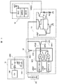
図5は本発明に係る電源装置の第3の実施例の構成を示すブロック図である。本実施例における電源装置は、電力制御回路52を除いて、第1の実施例と同様の構成である。
FIG. 5 is a block diagram showing the configuration of the third embodiment of the power supply apparatus according to the present invention. The power supply apparatus according to the present embodiment has the same configuration as that of the first embodiment except for the
ここで、図1と対応する部分には同一参照符号を付し、その重複説明を省略する。すなわち、電力制御回路52内に新たに第2の電源スイッチSW2と補助電源VBATが追加され、スイッチ制御回路520からは2つのスイッチ制御信号VCLとVCLBが出力される構成となっている。
Here, portions corresponding to those in FIG. 1 are denoted by the same reference numerals, and redundant description thereof is omitted. That is, a second power switch SW2 and an auxiliary power supply VBAT are newly added in the
電力制御回路52は、蓄電容量SCに充電されたエネルギの放電を制御する。第1の電源スイッチSW1、及び第2の電源スイッチSW2は、スイッチであれば特に限定するものではないが、PMOSFETを用いて実現しており、ゲート電圧が“L”の時にオンし、“H”の時にオフする。スイッチ制御回路520は、電源スイッチSW1を制御する制御信号VCLと電源スイッチSW2を制御するVCLB信号を出力する。VCLB信号は、制御信号VCLの反転信号である。従って、常に電源スイッチSW1とSW2のどちらか一方だけがオンしている。
The
電力制御回路52は、蓄電容量SCの充電電圧VDCを電圧監視回路DET1とDET2で監視し、充電電VDCが第1の所定電圧VH以上に充電されると、スイッチ制御回路520は制御信号VCLを“H”から“L”へ変化させ、蓄電容量SCに充電された充電エネルギを放電する。
The
この後、充電電圧VDCが第2の所定電圧VLに減少するまで放電は継続され、充電電圧VDCがVL以下になると、スイッチ制御回路520は制御信号VCLを、“L”から“H”へ制御し、蓄電容量SCの放電を停止する。制御信号VCLの反転信号であるVCLB信号を用いて補助電源VBATからの電力供給を制御しているので、蓄電容量SCからの放電が電源スイッチSW1により遮断されている場合は、レギュレータ13へは電源スイッチSW2により補助電源VBATから電力が供給される。
Thereafter, discharging is continued until the charging voltage VDC decreases to the second predetermined voltage VL. When the charging voltage VDC falls below VL, the
次に、本実施例の動作を説明する。
図6に本実施例の充電電圧VDC、制御信号VCL、レギュレータ出力電圧VREGの動作波形を示す。尚、図6において、横軸は時間であり、STは発電素子100による発電量PWRが強の場合、WKは発電量が弱の場合を示している。また、PSSは電力供給源から電力が供給されている期間を示し、この場合は蓄電容量SCおよび補助電源VBATからエネルギが供給されている期間を示している。
本実施例では、負荷14に常に電力が供給されるため、短時間だけ電力消費の大きなモードで動作することを特徴とする間欠動作を常に行っている。
Next, the operation of this embodiment will be described.
FIG. 6 shows operation waveforms of the charging voltage VDC, the control signal VCL, and the regulator output voltage VREG of this embodiment. In FIG. 6, the horizontal axis represents time, ST represents a case where the power generation amount PWR by the
In this embodiment, since power is always supplied to the
時刻Aで、発電が開始され、発電量PWRは強(ST)の状態である。蓄電容量SCが充電されるにつれて充電電圧VDCは上昇する。
時刻Bで、充電電圧VDCが第1の所定電圧VHに達するまでは電力制御回路52内の電源スイッチSW1を制御する信号VCLは“H”、電源スイッチSW2を制御する信号VCLBは“L”となり、電源スイッチSW1はオフし、SW2はオンしている。従って、時刻Bまでは補助電源VBATからレギュレータ13を通して電力が負荷14へ供給され、電源10から供給される電力は蓄電容量SCに充電される。時刻Bで充電電圧VDCが第1の所定電圧VHに達すると制御信号VCLは“L”、VCLB信号は“H”となり、電源スイッチSW2がオフして補助電源VBATからの電力供給が停止すると同時に電源スイッチSW1がオンして蓄電容量SCに充電された充電エネルギが放電され、レギュレータ13を通して電力が負荷14へ供給される。負荷14のセンサネット端末は、動作モードに応じた電力を消費する。蓄電容量SCの電力が負荷14へ供給されている期間は、消費電力に応じて充電電圧VDCは低下していく。図6の例では、時刻B−C間で信号処理SGを、C−D間で通信TXを行い、負荷14の消費電力に応じて充電電圧VDCが低下している。
At time A, power generation is started, and the power generation amount PWR is in a strong (ST) state. The charging voltage VDC increases as the storage capacity SC is charged.
Until the charging voltage VDC reaches the first predetermined voltage VH at time B, the signal VCL for controlling the power switch SW1 in the
時刻D以降、センサネット端末はタイマ動作TMに入る。タイマ動作は消費電力が小さいため、充電電圧VDCは回復していくが保護回路101によりツェナ電圧VLT以上には上昇しない。
After time D, the sensor network terminal enters the timer operation TM. Since the timer operation consumes little power, the charging voltage VDC recovers but does not rise above the Zener voltage VLT by the
時刻G以降では、発電環境の変化により電源10の発電量PWRが低下し、弱(WK)の状態である。そのため、センサネット端末が間欠的な動作を続けるに従って充電電圧VDCは徐々に低下していく。
After time G, the power generation amount PWR of the
時刻Pでは、遂に第2の所定電圧VLまで低下してしまう。充電電圧VDCがVL以下になると、再び制御信号VCLは“H”を出力して電源スイッチSW1をオフし、蓄電容量SCの放電を停止する。同時に、VCLB信号は“L”を出力して電源スイッチSW2をオンし、補助電源VBATから負荷14へ電力を供給する。一度、充電電圧VDCがVL以下になると、充電電圧VDCが再びVH以上に充電される時刻Qになるまで、補助電源VBATが負荷を駆動する電力を供給し、電源10が発生する電力は蓄電容量SCの充電にのみ充てられる。
At time P, the voltage finally drops to the second predetermined voltage VL. When the charging voltage VDC becomes equal to or lower than VL, the control signal VCL again outputs “H”, turns off the power switch SW1, and stops discharging the storage capacitor SC. At the same time, the VCLB signal outputs “L”, turns on the power switch SW2, and supplies power from the auxiliary power supply VBAT to the
このように自然エネルギを用いて発電した電力を容量に充電し、充電電圧をVLとVHの2電圧で監視して蓄電容量から負荷への放電をヒステリシス制御することにより、負荷回路の動作エネルギを効率よく十分に確保できる。さらに、充電された電力が減少して負荷を駆動できなくなった場合、接続されている補助電源から電力が供給されるため、負荷回路を常に動作させることが可能である。したがって、微弱な電源を用いて消費電力が過大な負荷を駆動できる電源装置を実現できる。また、電源の発電量が不安定な場合でも常に負荷へ電力を供給できる。本実施例は補助電源を備えたことにより負荷への給電が停止することがないため、情報を常に保持する必要がある用途に適用できる。 In this way, the power generated using natural energy is charged into the capacity, the charging voltage is monitored with two voltages VL and VH, and the discharge from the storage capacity to the load is controlled by hysteresis, thereby reducing the operating energy of the load circuit. It can be secured efficiently and sufficiently. Furthermore, when the charged power is reduced and the load cannot be driven, power is supplied from the connected auxiliary power supply, so that the load circuit can always be operated. Therefore, a power supply device that can drive a load with excessive power consumption using a weak power source can be realized. Further, even when the power generation amount of the power source is unstable, it is possible to always supply power to the load. Since the power supply to the load does not stop due to the provision of the auxiliary power supply, the present embodiment can be applied to an application in which information needs to be constantly maintained.
10…電源、12,32,52…電力制御回路、14…負荷、100…発電素子(GE)、101…保護回路、120,320,520…スイッチ制御回路、AM…振動振幅値、BST…基地局、BUF…バッファ、D…ダイオード、DET1,DET2…電圧監視回路、I1…電流源、IL…照度、LVC…レベル変換回路、MPRO…マイクロプロセッサ、MNGSV…管理サーバ、n12,n34…ノード、N1〜N3…NANDゲート、NTWK…ネットワーク、OP_MOD…動作モード、PSS…電力供給源、PWR…発電量、PWR_C…消費電力、Q1〜Q3…NPNトランジスタ、R1〜R7…抵抗、RAD…無線、SC…蓄電容量、SEN…センシング、SENS…センサ、SENSTM…センサネット端末、SG…信号処理、SW1,SW2…電源スイッチ、T1,T2…端子、TX…通信、VBAT…補助電源、VCLB…反転制御信号、VCL…制御信号、VREF…基準電圧、VDC…充電電圧、VDEC…電圧監視回路出力、VREG…レギュレータ出力、ZD…ツェナダイオード。
DESCRIPTION OF
Claims (8)
前記蓄電容量の充電電圧である第1及び第2の所定電圧に基づき前記蓄電容量に充電された充電エネルギの放電及び停止を制御する電力制御回路と、
前記電力制御回路の制御により放電された前記充電エネルギを用いて所定の電圧を負荷へ出力するレギュレータとを有し、
前記充電エネルギが前記第1の所定電圧以上の場合には、前記負荷を駆動するために前記充電エネルギの放電を可能とし、前記充電エネルギが前記第1の所定電圧よりも小さい前記第2の所定電圧以下の場合には、前記充電エネルギの前記負荷を駆動するための放電を停止することを特徴とする電源装置。 A storage capacity for charging the supplied energy;
A power control circuit for controlling discharge and stop of charging energy charged in the storage capacity based on first and second predetermined voltages that are charging voltages of the storage capacity;
A regulator that outputs a predetermined voltage to a load using the charging energy discharged by the control of the power control circuit;
When the charging energy is equal to or higher than the first predetermined voltage, the charging energy can be discharged to drive the load, and the charging energy is smaller than the first predetermined voltage. When the voltage is equal to or lower than the voltage, discharging for driving the load of the charging energy is stopped.
前記蓄電容量に供給されるエネルギは、
自然エネルギを利用して発電する発電素子と、
前記発電素子の出力と接地電位との間に直列にカソード同士を接続したダイオードとツェナダイオードとを含んでなる前記発電素子への逆流を防ぐ保護回路とを有する電源から供給されることを特徴とする電源装置。 The power supply device according to claim 1,
The energy supplied to the storage capacity is
A power generation element that generates power using natural energy;
It is supplied from a power source having a protection circuit for preventing backflow to the power generation element, which includes a diode having a cathode connected in series between the output of the power generation element and a ground potential, and a Zener diode. Power supply.
前記電力制御回路は、
前記蓄電容量と前記レギュレータとの間に設けられた第1電源スイッチと、
前記第1の所定電圧を検出する第1電圧監視回路と、
前前記第1の所定電圧より低い第2の所定電圧を検出する第2電圧監視回路と、
前記第1及び第2の電圧監視回路の出力に基づき前記第1電源スイッチを制御するスイッチ制御回路とを有し、
前記スイッチ制御回路は、前記第1電圧監視回路の検出信号に基づき前記第1電源スイッチをオン状態にして前記充電エネルギの放電を開始させ、前記第2の電圧監視回路の検出信号に基づき前記第1電源スイッチをオフ状態にして前記充電エネルギの放電を停止するように前記第1電源スイッチを制御することを特徴とする電源装置。 The power supply device according to claim 1,
The power control circuit includes:
A first power switch provided between the storage capacity and the regulator;
A first voltage monitoring circuit for detecting the first predetermined voltage;
A second voltage monitoring circuit for detecting a second predetermined voltage lower than the first predetermined voltage before;
A switch control circuit for controlling the first power switch based on the outputs of the first and second voltage monitoring circuits;
The switch control circuit turns on the first power switch based on the detection signal of the first voltage monitoring circuit to start discharging the charging energy, and the first control switch starts the discharging of the charging energy, based on the detection signal of the second voltage monitoring circuit. 1. The power supply apparatus according to claim 1, wherein the first power switch is controlled to turn off one power switch to stop discharging the charging energy.
前記スイッチ制御回路は、
前記第2の電圧監視回路の前記第2の所定電圧検出信号に基づき前記充電エネルギが減少したことを示す警告信号を前記負荷へ送信する手段と、所定の時間後に前記第1電源スイッチをオフする手段とをさらに具備することを特徴とする電源装置。 The power supply device according to claim 3,
The switch control circuit includes:
Means for transmitting to the load a warning signal indicating that the charge energy has decreased based on the second predetermined voltage detection signal of the second voltage monitoring circuit; and turning off the first power switch after a predetermined time. And a power supply apparatus.
前記電力制御回路は、
補助電源と
前記補助電源と前記レギュレータとの間に設けられた第2の電源スイッチとをさらに具備し、
前記スイッチ制御回路は、
前記第1電圧監視回路の検出信号に基づき前記第2電源スイッチをオフすると共に前記第1電源スイッチをオンして前記充電エネルギを放電させ、その後、前記第2監視回路の検出信号に基づいて前記第1電源スイッチをオフして放電を停止させると共に前記第2電源スイッチをオンして前記補助電源からエネルギを前記レギュレータへ供給するように第1及び第2電源スイッチを制御することを特徴とする電源装置。 The power supply device according to claim 1,
The power control circuit includes:
An auxiliary power source, and a second power switch provided between the auxiliary power source and the regulator,
The switch control circuit includes:
Based on the detection signal of the first voltage monitoring circuit, the second power switch is turned off and the first power switch is turned on to discharge the charging energy, and then based on the detection signal of the second monitoring circuit The first power switch is turned off to stop discharging, and the second power switch is turned on to control the first and second power switches to supply energy from the auxiliary power to the regulator. Power supply.
前記負荷は、所定のデータを検出するセンサと、信号を処理するマイクロプロセッサと、前記データを送受信する無線回路とを備え、消費電力が大きく異なる複数の動作モードを持ち、大部分の時間はわずかな電力しか消費しない小電力モードで動作し、間欠的に短期間だけ前記大きく電力を消費する大電力モードで動作することを特徴とする電源装置。 The power supply device according to claim 1,
The load includes a sensor for detecting predetermined data, a microprocessor for processing a signal, and a wireless circuit for transmitting and receiving the data, and has a plurality of operation modes with greatly different power consumption, and most of the time is little. A power supply apparatus that operates in a low-power mode that consumes only a small amount of power and operates in a high-power mode that consumes a large amount of power intermittently for a short period of time.
前記負荷は、所定のデータを検出するセンサと、信号を処理するマイクロプロセッサと、前記データを送受信する無線回路とを備え、消費電力が大きく異なる複数の動作モードを持ち、大部分の時間はわずかな電力しか消費しない小電力モードで動作し、間欠的に短期間だけ前記大きく電力を消費する大電力モードで動作する負荷であって、
前記スイッチ制御回路が出力する前記警告信号が入力されると、前記負荷の動作中の動作モードを変更し、あらかじめ決められた処理を行うことを特徴とする電源装置。 The power supply device according to claim 4,
The load includes a sensor for detecting predetermined data, a microprocessor for processing a signal, and a wireless circuit for transmitting and receiving the data, and has a plurality of operation modes with greatly different power consumption, and most of the time is little. A load that operates in a low power mode that consumes only a small amount of power and operates in a large power mode that consumes a large amount of power intermittently for a short period of time,
When the warning signal output from the switch control circuit is input, an operation mode during operation of the load is changed to perform a predetermined process.
前記負荷は前記スイッチ制御回路が出力する前記警告信号が入力されると、基地局へ停止信号を発信することを特徴とする電源装置。 The power supply device according to claim 7,
The power supply apparatus according to claim 1, wherein when the warning signal output from the switch control circuit is input, the load transmits a stop signal to a base station.
Priority Applications (1)
| Application Number | Priority Date | Filing Date | Title |
|---|---|---|---|
| JP2004058522A JP2005253166A (en) | 2004-03-03 | 2004-03-03 | Power unit |
Applications Claiming Priority (1)
| Application Number | Priority Date | Filing Date | Title |
|---|---|---|---|
| JP2004058522A JP2005253166A (en) | 2004-03-03 | 2004-03-03 | Power unit |
Publications (2)
| Publication Number | Publication Date |
|---|---|
| JP2005253166A true JP2005253166A (en) | 2005-09-15 |
| JP2005253166A5 JP2005253166A5 (en) | 2006-11-02 |
Family
ID=35033126
Family Applications (1)
| Application Number | Title | Priority Date | Filing Date |
|---|---|---|---|
| JP2004058522A Pending JP2005253166A (en) | 2004-03-03 | 2004-03-03 | Power unit |
Country Status (1)
| Country | Link |
|---|---|
| JP (1) | JP2005253166A (en) |
Cited By (6)
| Publication number | Priority date | Publication date | Assignee | Title |
|---|---|---|---|---|
| JP2007043513A (en) * | 2005-08-04 | 2007-02-15 | Tdk Corp | Radio transmitter |
| CN102059957A (en) * | 2009-11-18 | 2011-05-18 | 株式会社日立制作所 | Control system for electric vehicle and electric vehicle equipped therewith |
| JP2013038941A (en) * | 2011-08-09 | 2013-02-21 | Nippon Dengyo Kosaku Co Ltd | Charge voltage control circuit and power supply circuit |
| CN107979365A (en) * | 2016-10-24 | 2018-05-01 | 富士施乐株式会社 | Electronic device |
| US10411612B2 (en) | 2017-03-21 | 2019-09-10 | Kabushiki Kaisha Toshiba | Power generation system for self activation |
| WO2022097199A1 (en) * | 2020-11-04 | 2022-05-12 | 三菱電機株式会社 | Semiconductor device, and multi-rotation encoder |
-
2004
- 2004-03-03 JP JP2004058522A patent/JP2005253166A/en active Pending
Cited By (6)
| Publication number | Priority date | Publication date | Assignee | Title |
|---|---|---|---|---|
| JP2007043513A (en) * | 2005-08-04 | 2007-02-15 | Tdk Corp | Radio transmitter |
| CN102059957A (en) * | 2009-11-18 | 2011-05-18 | 株式会社日立制作所 | Control system for electric vehicle and electric vehicle equipped therewith |
| JP2013038941A (en) * | 2011-08-09 | 2013-02-21 | Nippon Dengyo Kosaku Co Ltd | Charge voltage control circuit and power supply circuit |
| CN107979365A (en) * | 2016-10-24 | 2018-05-01 | 富士施乐株式会社 | Electronic device |
| US10411612B2 (en) | 2017-03-21 | 2019-09-10 | Kabushiki Kaisha Toshiba | Power generation system for self activation |
| WO2022097199A1 (en) * | 2020-11-04 | 2022-05-12 | 三菱電機株式会社 | Semiconductor device, and multi-rotation encoder |
Similar Documents
| Publication | Publication Date | Title |
|---|---|---|
| JP3962524B2 (en) | Discharge control circuit | |
| US9590451B2 (en) | Autonomous power supply system | |
| JP5803446B2 (en) | Semiconductor integrated circuit, protection circuit and battery pack | |
| JP4720704B2 (en) | Power supply switching circuit | |
| EP3923441A1 (en) | Battery controller, wireless battery control system, battery pack, and battery balancing method | |
| JP2019149904A (en) | Power supply controller and communication apparatus | |
| US20070013345A1 (en) | Device and method for controlling a current supply | |
| CN109904886B (en) | Control circuit module and control method thereof | |
| CN113728489B (en) | Battery controller, wireless battery control system, battery pack and battery balancing method | |
| JP3872057B2 (en) | Battery device overvoltage protection circuit | |
| Unterassinger et al. | A power management unit for ultra-low power wireless sensor networks | |
| JP2005253166A (en) | Power unit | |
| JP2005012958A (en) | Battery device | |
| JP4435000B2 (en) | Battery control circuit, electronic device equipped with the battery control circuit, charge control program, and charge control method | |
| JP2007151322A (en) | Power circuit and dc-dc converter | |
| JP2019103305A (en) | Power supply device and communication device | |
| JP2008191888A (en) | Photosensor radio tag and photosensor system with the photosensor radio tag | |
| JP6784399B2 (en) | Battery power supply, shutdown circuit, and shutdown method | |
| JP6426804B2 (en) | Battery monitoring system and battery monitoring device | |
| JP2020088907A (en) | Power supply device and communication apparatus | |
| JP4522738B2 (en) | Power-on reset device and electronic device | |
| JPH10210681A (en) | Power controller and electronic appliance having the same | |
| EP1429442A2 (en) | Circuit for preventing unintentional power off of mobile terminal and method therefor | |
| JPH116885A (en) | Electronic apparatus provided with generator means | |
| JP4527560B2 (en) | DC power supply method and apparatus using charging circuit |
Legal Events
| Date | Code | Title | Description |
|---|---|---|---|
| A521 | Written amendment |
Free format text: JAPANESE INTERMEDIATE CODE: A523 Effective date: 20060912 |
|
| A621 | Written request for application examination |
Free format text: JAPANESE INTERMEDIATE CODE: A621 Effective date: 20060912 |
|
| RD02 | Notification of acceptance of power of attorney |
Free format text: JAPANESE INTERMEDIATE CODE: A7422 Effective date: 20060912 |
|
| A977 | Report on retrieval |
Free format text: JAPANESE INTERMEDIATE CODE: A971007 Effective date: 20070925 |
|
| A131 | Notification of reasons for refusal |
Free format text: JAPANESE INTERMEDIATE CODE: A131 Effective date: 20071002 |
|
| A521 | Written amendment |
Free format text: JAPANESE INTERMEDIATE CODE: A523 Effective date: 20071203 |
|
| A02 | Decision of refusal |
Free format text: JAPANESE INTERMEDIATE CODE: A02 Effective date: 20080729 |