JP2005244084A - Spiral high-frequency coil and manufacturing method thereof - Google Patents
Spiral high-frequency coil and manufacturing method thereof Download PDFInfo
- Publication number
- JP2005244084A JP2005244084A JP2004054587A JP2004054587A JP2005244084A JP 2005244084 A JP2005244084 A JP 2005244084A JP 2004054587 A JP2004054587 A JP 2004054587A JP 2004054587 A JP2004054587 A JP 2004054587A JP 2005244084 A JP2005244084 A JP 2005244084A
- Authority
- JP
- Japan
- Prior art keywords
- conductor line
- conductor
- recess
- line
- providing
- Prior art date
- Legal status (The legal status is an assumption and is not a legal conclusion. Google has not performed a legal analysis and makes no representation as to the accuracy of the status listed.)
- Pending
Links
Images


Landscapes
- Manufacturing Cores, Coils, And Magnets (AREA)
- Coils Or Transformers For Communication (AREA)
Abstract
Description
この発明は微細加工技術によるらせん状高周波コイルとその製造方法に関するものである。 The present invention relates to a spiral high-frequency coil by a microfabrication technique and a manufacturing method thereof.
従来の高周波コイルは複数のループ状線路を軸線が共通になるように配列したらせん状に形成されている。そのらせん状体の両端部は軸方向に屈曲されて入力部と出力部に形成されていて、これら入出力部が基板に保持されている。
次に動作について説明する。
信号の入力部から入力された高周波信号はループ状線路へと伝送され、信号の出力部から出力される。このとき、1つのループ状線路の周囲に発生する磁界の向きはその他のループ状線路の発生する磁界の向きと同じであり、ループ状線路全体では電流の変化を妨げる向きに電位が発生し、インダクタとして働く。また、電磁界はループ状線路の内側に集中するので基板の影響を受けにくいため、基板の誘電正接による損失は少なく、低損失なコイルとして働く。
次に従来の高周波コイルの加工方法について説明する。
アルミナ基板の上に厚さ30μmのポリイミド膜を積層した後、アルミニウムをマスクとしたエッチングにより溝を形成して銅メッキを行うことにより、入出力部を形成する。さらにポリイミド膜を積層し、アルミニウムをマスクとしたエッチングにより溝を形成して銅メッキを行うことによりループ状線路の下方部を形成する。次いでポリイミド膜を積層し、アルミニウムをマスクとしたエッチングにより溝を形成して銅メッキを行うことによりループ状線路の垂直部を作成する。最後に、ポリイミド膜を積層し、アルミニウムをマスクとしたエッチングにより溝を形成して銅メッキを行うことによりループ状線路の上方部を形成する(例えば、非特許文献1、特にFig.9a〜e参照)。
他の従来の高周波コイルでは、グランド導体の上にシリコンが堆積されたシリコン基板を設け、シリコン基板の上に薄い誘電体膜を形成し、誘電体膜の上にスパイラルコイル、スパイラルコイルの入出力部およびスパイラルコイルの終端部分と入出力部を結ぶエアブリッジが設けられ、かつスパイラルコイルよりも下方のシリコンはエッチングにより除去されて空孔に形成されている。
次に動作について説明する。
入力部から入力された信号はスパイラルコイルに導かれ、さらに信号はエアブリッジを介して出力部へ導かれる。スパイラルシリコンの下方は空孔に形成されているため、シリコンの誘電体損やシリコンの導体損が生ぜず、このため小型で低損失なコイルが実現できる(例えば、非特許文献2、特にFig.2参照)。
A conventional high-frequency coil is formed in a spiral shape by arranging a plurality of loop-shaped lines so that their axes are common. Both ends of the spiral body are bent in the axial direction to form an input portion and an output portion, and these input / output portions are held by the substrate.
Next, the operation will be described.
The high-frequency signal input from the signal input unit is transmitted to the loop-shaped line and output from the signal output unit. At this time, the direction of the magnetic field generated around one loop-shaped line is the same as the direction of the magnetic field generated by the other loop-shaped lines, and a potential is generated in a direction that prevents the current from changing in the entire loop-shaped line. Works as an inductor. In addition, since the electromagnetic field is concentrated inside the loop-shaped line, it is not easily affected by the substrate, so that the loss due to the dielectric loss tangent of the substrate is small and the coil works as a low-loss coil.
Next, a conventional method for processing a high-frequency coil will be described.
After laminating a polyimide film having a thickness of 30 μm on the alumina substrate, a groove is formed by etching using aluminum as a mask, and copper plating is performed to form an input / output portion. Further, a polyimide film is laminated, a groove is formed by etching using aluminum as a mask, and copper plating is performed to form a lower portion of the loop-shaped line. Next, a polyimide film is laminated, a groove is formed by etching using aluminum as a mask, and copper plating is performed to create a vertical portion of the loop-shaped line. Finally, a polyimide film is laminated, a groove is formed by etching using aluminum as a mask, and copper plating is performed to form an upper portion of the loop-shaped line (for example, Non-Patent Document 1, FIG. 9a to e). reference).
In other conventional high-frequency coils, a silicon substrate on which silicon is deposited is provided on a ground conductor, a thin dielectric film is formed on the silicon substrate, and a spiral coil and spiral coil input / output are formed on the dielectric film. And an air bridge connecting the terminal portion of the spiral coil and the input / output portion, and silicon below the spiral coil is removed by etching to form a void.
Next, the operation will be described.
The signal input from the input unit is guided to the spiral coil, and further the signal is guided to the output unit via the air bridge. Since the lower part of the spiral silicon is formed as a hole, silicon dielectric loss and silicon conductor loss do not occur, so that a small and low-loss coil can be realized (see, for example, Non-Patent
非特許文献1に記載の技術では、微細加工技術を用いて基板上にポリイミド膜を何層にも積み上げて高周波コイルを下方部から順次形成するので、加工工程が複雑でコストがかかるという課題があった。
また、非特許文献2に記載の技術では、複数枚のウェハを張り合わせて加工するので、部品の厚みが厚くなるという課題があった。
In the technique described in Non-Patent Document 1, since the high-frequency coil is sequentially formed from the lower part by stacking multiple layers of polyimide films on the substrate using a fine processing technique, there is a problem that the processing process is complicated and expensive. there were.
Moreover, in the technique described in
この発明は上記のような課題を解決するためになされたもので、加工工程が簡易でコスト低減が図れ、かつ部品の薄型化が実現可能な高周波コイルとその製造方法を得ることを目的とする。 The present invention has been made to solve the above-described problems, and an object of the present invention is to obtain a high-frequency coil and a method for manufacturing the same that can simplify the machining process, reduce the cost, and realize a thinner part. .
この発明に係るらせん状高周波コイルは、凹部を持つ基板と、凹部の窪んだ部分の表面に接することなくそれぞれ略並行に設けられた複数の第1の導体線路と、凹部の上面部分と同一面の開口面上に設けられた絶縁体と、絶縁体の上面にそれぞれ略並行に架設された複数の第2の導体線路と、第1の導体線路の一端を第2の導体線路の一端に接続する第1の接続部と、第1の導体線路の他端を一端が接続された第2の導体線路の隣の第2の導体線路の一端に接続する第2の接続部とを備えたものである。 The spiral high-frequency coil according to the present invention includes a substrate having a recess, a plurality of first conductor lines provided substantially in parallel without contacting the surface of the recessed portion of the recess, and the upper surface portion of the recess. An insulator provided on the opening surface, a plurality of second conductor lines installed substantially parallel to the top surface of the insulator, and one end of the first conductor line connected to one end of the second conductor line And a second connection portion for connecting the other end of the first conductor line to one end of the second conductor line adjacent to the second conductor line to which one end is connected. It is.
この発明によれば、らせん状導体線路の半分以上は基板の凹部内面の窪んだ部分に設けられ、しかも他の部分の導体線路は凹部の開口面に架設されているので、らせん状導体のほぼ全体が基板の凹部内部に保持されていることになり、したがって、らせん状導体自体の強度や剛性が多少低くても高周波コイルを形成することが可能であり、よって、らせん状導体線路をより薄くかつ細く形成することができるため小型化が可能となるとともに、高周波コイル全体の厚さは基板の高さにほぼ等しく、したがって、全体の厚さを薄くすることができる。
また、第1の導体線路が凹部の窪んだ部分の表面に接することがないから、第1の導体線路が空気に囲まれているため、凹部の窪んだ部分の表面に第1の導体線路に接している場合と比較しても、より低損失とすることができる。
According to the present invention, more than half of the helical conductor line is provided in the recessed portion of the inner surface of the concave portion of the substrate, and the other portion of the conductor line is installed on the opening surface of the concave portion. The whole is held inside the concave portion of the substrate. Therefore, it is possible to form a high-frequency coil even if the strength and rigidity of the spiral conductor itself are somewhat low, and thus the spiral conductor line is made thinner. Since it can be formed thin, the size can be reduced, and the entire thickness of the high-frequency coil is substantially equal to the height of the substrate, and therefore the overall thickness can be reduced.
In addition, since the first conductor line does not contact the surface of the recessed portion of the recess, the first conductor line is surrounded by air, so that the first conductor line is formed on the surface of the recessed portion of the recess. Even when compared with the case of contact, the loss can be further reduced.
以下、この発明の実施の一形態を説明する。
実施の形態1.
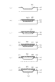
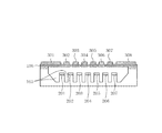
図1はこの発明の実施の形態1による高周波コイルの斜視図、図2、図3は製造工程の途中を示す斜視図である。図4は、第1の導体線路に沿った断面図で製造工程を示す図である。図6は、図1のAA’断面を示す断面図である。シリコン基板100の表面には絶縁膜105が設けられ、絶縁膜105が設けられた面にはエッチングにより微小な凹部102が形成されている。凹部102の設けられた面にはエッチングされた窪みのある部分、即ち凹部の内面と、エッチングされていない、即ち、窪んでいない部分である凹部の上部上面から構成されている。この凹部の内部の窪んだ部分の表面に接することなくそれぞれ略並行に設けられた複数の第1の導体線路である複数の第1の金の線201〜207が配置されている。
また、凹部102の上部上面部分と同一面の開口面上には、絶縁膜106が設けられており、絶縁膜106の上面には、それぞれ略並行に架設された複数の第2の導体線路である複数の第2の金の線及び入出力部となる金の線301〜308が形成されている。そして第1の金の線201〜207の一端を第2の金の線301〜308の一端に接続する第1の接続部401と、第1の金の線の他端を一端が接続される第2の金の線の隣の第2の金の線の一端に接続する第2の接続部402を複数設けることにより、隣り合う第1の金の線同士が第2の金の線により電気的に接続される。第1の接続部及び第2の接続部は、接続が容易となるように凹部の上段上面に設けられている。複数の第1の金の線及び複数の第2の金の線が一本の導体となり、金の線はらせん状のコイルに形成される。金の線で形成されたらせん状のコイルのコア部は中空に構成されている。
絶縁膜105の上面、凹部102の近傍には、第2の金の線302〜307とほぼ直交する方向に伸びる測定用グラウンドパッド501及び502が設けられている。
An embodiment of the present invention will be described below.
Embodiment 1 FIG.
1 is a perspective view of a high-frequency coil according to Embodiment 1 of the present invention, and FIGS. 2 and 3 are perspective views showing the middle of a manufacturing process. FIG. 4 is a cross-sectional view along the first conductor line showing the manufacturing process. FIG. 6 is a cross-sectional view showing a cross section AA ′ of FIG. An
In addition, an
次に上記構成に係る高周波コイルの製造方法について説明する。
まず、図2に示すように絶縁膜105が設けられたシリコン基板100の表面にウェットエッチングを施して深さ30μmほどの凹部102を設ける。次に図3に示すようにこの凹部102の内面から基板100の上面にかけて金をスパッタし、フォトエッチングにより1μmほどの厚みの複数の第1の金の線201〜207を残す。このとき、各々の第1の金の線201〜207の両端がシリコン基板100の凹部の上段上面にわずかに残るようにしておく(図4(a)参照。)。
Next, the manufacturing method of the high frequency coil which concerns on the said structure is demonstrated.
First, as shown in FIG. 2, the surface of the
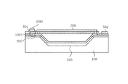
次に、犠牲層としてたとえばフォトレジスト1000を凹部102に充填してシリコン基板100の凹部の上面と同じ面で平坦化する。このとき、第1の金の線201〜207の各々の両端部が犠牲層から露出するようにする(図4(b))。
次いで窒化シリコンの薄膜からなる第1の絶縁体の膜106をスパッタし、フォトエッチングにより凹部102の開口面よりも少し大きくパターニングする。次いで前工程で形成した第1の金の線201〜207の両端部が絶縁体から露出するようにエッチングし、同時に犠牲層を取り除くための図示しない穴を絶縁体にあけておく(図4(c))。次に第1の絶縁体の膜102の上に金をスパッタし、フォトエッチングにより1μmほどの厚みの第2の金の線及び入出力部となる金の線301〜308及び測定用グラウンドパッド501及び502をパターニングする。
その際、第2の金の線及び入出力部となる金の線301〜308の各々の両端部が第1の金の線201〜207の各々の両端部に接合させるための第1及び第2の接続部401,402を形成する(図4(d))。上述したように第1及び第2の接続部401,402を形成することにより、隣り合う第1の金の線同士が第2の金の線により電気的に接続される。
Next, as a sacrificial layer, for example, a photoresist 1000 is filled in the
Next, a
At this time, first and second gold wires and first and
最後に犠牲層として凹部102に充填されているフォトレジスト1000をウェットエッチングで、第1の金の線の下部の基板材103をドライエッチングにより取り除くことで第1及び第2の金の線301,201,302,202,303,203,304,204,305,205,306,206,307,207,308は連続する一本のらせん状導体となり、全体としてらせん状導体の内部が中空で、第1の金の線201〜207の両端を除く部分が基板100と接することなく空中にうかんだ状態となるコイルが得られる。図4(e)及び図5は犠牲層のみが除去された状況を示す図で、図4(f)及び図6は、犠牲層のみならず、第1の金の線の下部の基板材103も除去された状況を示す図である。
凹部内に犠牲層を充填し、犠牲層上に第1の絶縁体の膜102及び第2の金の線を形成した後、凹部に充填された犠牲層を除去するので、工程の簡略化が図れてコスト低減が可能となるとともに、全体の厚さを薄くすることができる。
第1の金の線が基板100と接することなく空中にうかんだ状態で、第1の導体線路が空気に囲まれているため、凹部の窪んだ部分の表面に第1の導体線路に接している場合と比較しても、より低損失とすることができる。
Finally, the
The sacrificial layer is filled in the recess, and after the
Since the first conductor line is surrounded by air in a state where the first gold wire is tangled in the air without contacting the
次に動作について説明する。
らせん状導体の入力端子となる金の線305から高周波信号が入力されると、この高周波信号は金の線を201,302,202,303,203,304,204,305,205,306,206,307,207の順で伝達され、金の線308から出力される。このように電流がらせん状に流れるため、第2の金の線302〜307に流れる電流の向きは等しく、また、第1の金の線201〜207に流れる電流の向きも等しくなる。これにより凹部102の中に磁界が閉じ込められるように発生するが、この部分は中空になり、また第1の金の線が基板と接していないため損失がほとんどない。このためこの微小ならせん状導体は低損失となる。
凹部102の開口面積が大きいものであっても第2の金の線及び入出力部となる金の線301〜308が第1の絶縁体の膜104により支えられるためらせん状導体の作製が容易になる。
Next, the operation will be described.
When a high-frequency signal is input from a
Even if the opening area of the
基板100としてはシリコンに限定されることなく、ガラス、GaAs、アルミなど微細な加工が可能な材料であれば利用できる。また、金の線は金に限定されることなく、例えばフォトリソグラフィー技術によりパターンが作成できるものなら利用できる。金の線の厚みは用いられる金属の導電率及び利用する周波数を考慮し表皮深さ以上であることが望ましい。
The
なお、上記実施の形態1では第1の絶縁体の膜102の上に第2の金の線及び入出力部となる金の線301〜308を形成しているが、これに限らず第2の金の線及び入出力部となる金の線301〜308を第1の絶縁体の膜106の上に設けず犠牲層の上に直接設けるようにしてもよい。図7は、犠牲層の上に第2の金の線を直接設け、その後の犠牲層を取り除く等の工程をほぼ同様に行うことにより作成したらせん状コイル装置を示す斜視図である。
第1の絶縁体の膜を設ける工程等を省略することができ、より簡易に作成することができる。
また、凹部の窪んだ部分の内面の基板をエッチングする際に、エッチングされない薄膜、例えば、酸化膜104などを凹部の窪み内部傾斜面に設け、基板のエッチング面積を少し減らし、微小コイルの機械的な強度を上げた構造とすることができる。図8は犠牲層のみが除去された状況を示す断面図で、図9は、犠牲層のみならず第1の金の線の下部の基板材103も除去された状況を示す断面図である。図7と図9を比べるとわかるように、酸化膜104の下部の基板がエッチングされることがないので、図7の実施例に比べても基板の機械的強度が高いことがわかる。
また、犠牲層除去用穴を通して凹部内部窪んだ部分の第1の金の線と接触している基板のエッチングが容易ではない場合、凹部内部窪んだ部分に形成された第1の金の線の間の基板を予めエッチングし、第1の金の線の下部にトレンチ105を持つ構造とすることもできる。図10は第1の金の線の間の基板をエッチングした後に、犠牲層を充填する方法で作られたものの断面図である。
図1〜図7で説明した実施例の作成方法において、充填層を充填する前に、上述したトレンチを作成する工程を加え、犠牲層を除去する後の工程の第1の金の線の下部の基板材103も除去する工程を行わないだけで、図10に示すようなトレンチを備えたらせん状コイルを作成することができる。図7に示すような第1の金の線の下部が完全に除去されているものに比べれば、損失が大きくなるが、基板がガラスである場合などエッチングが比較的困難な材料であっても、容易に制作することができる。
第1及び第2の金の線を7本及び6本用いたものについて説明したが、第1及び第2の金の線の数は、その用途等により適宜変更することも可能である。
第1の金の線の下部の基板材103、全ての部分(基板の上部上面部分を除く)を除去する例を示したが、全ての部分でなく、一部基板に保持されるようにしても良い。その場合、第1の金の線の一部が基板に保持され、コイルが頑丈な構造となる。
In the first embodiment, the second gold wire and the
The step of providing the first insulator film and the like can be omitted, and the first insulator can be formed more easily.
In addition, when etching the substrate on the inner surface of the recessed portion of the recess, an unetched thin film, for example, an
In addition, when it is not easy to etch the substrate that is in contact with the first gold line in the recessed portion inside through the sacrificial layer removal hole, the first gold line formed in the recessed portion in the recessed portion is not easily etched. The substrate in between may be pre-etched to have a structure having a
1 to 7, in the method for producing the embodiment described above, before the filling layer is filled, the step of creating the trench described above is added, and the lower part of the first gold line in the step after the sacrifice layer is removed A spiral coil having a trench as shown in FIG. 10 can be formed by simply not performing the process of removing the
Although the description has been given of the case where seven and six first and second gold wires are used, the number of the first and second gold wires may be changed as appropriate depending on the application.
Although the example of removing the
また、凹部に形成されてある金の線の一端を一方向または交互対称に延ばし、延ばした先の一部分と測定用グラウンドパッド501あるいは502を窒化シリコン1001などの誘電体に挟むことにより、コンデンサを設けることも可能である。図11は、金の線の一端を延ばし、その先端の一部の上に窒化シリコン1001を、窒化シリコン1001の上に測定用グラウンドパッド501を設けコンデンサ1002とした例を示す。測定用グランドパッドの上に窒化シリコンを設け、窒化シリコンの上に金の線を設けることによりコンデンサとしても良い。
In addition, one end of the gold wire formed in the recess is extended in one direction or alternately symmetrically, and a part of the extended tip and the
実施の形態2.
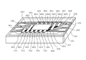
図12はこの発明の実施の形態2による高周波コイルの斜視図である。シリコン基板100の表面には絶縁膜105が設けられ、絶縁膜105が設けられた面にはエッチングにより微小な凹部102が形成されている。凹部102の設けられた面にはエッチングされた窪みのある部分、即ち凹部の内面と、エッチングされていない、即ち、窪んでいない部分である凹部の上部上面から構成されている。この凹部の内部の窪んだ部分の表面に接することなくそれぞれ略並行に設けられたた複数の第1の導体線路である複数の第1の金の線701,703,705と、それぞれ略並行に設けられた複数の第3の導体線路である複数の第3の金の線702,704,706が、交互に配置されている。
また、凹部102の上部上面部分と同一面の開口面上には、絶縁膜106が設けられており、絶縁膜106の上面には、それぞれ略並行に架設された複数の第2の導体線路である複数の第2の金の線603,605と、それぞれ略並行に架設された複数の第4の導体線路である、複数の第4の金の線604,606とが交互に配置されている。
そして第1の金の線の一端を第2の金の線の一端に接続する第1の接続部403と、第1の金の線の他端を一端が接続する第2の金の線の隣の第2の金の線の一端に接続する第2の接続部404を複数設けることにより、隣り合う第1の金の線が第2の金の線により接続される。また、第3の金の線の一端を第4の金の線の一端に接続する第3の接続部405と、第3の金の線の他端を一端が接続する第4の金の線の隣の第4の金の線の一端に接続する第4の接続部406を複数設けることにより、隣り合う第3の金の線が第4の金の線により接続される。
第1〜4の接続部は、接続が容易となるように凹部の上段上面に設けられている。そして、複数の第1の金の線及び複数の第2の金の線が一本の導体となり、第1のらせん状のコイルに形成される。また、複数の第3の金の線及び複数の第4の金の線が一本の導体となり、第2のらせん状のコイルに形成される。そして、金の線で形成されたら第1及び第2のらせん状のコイルのコア部は中空に構成されている。
FIG. 12 is a perspective view of a high-frequency coil according to
In addition, an insulating
Then, a first connecting
The 1st-4th connection part is provided in the upper stage upper surface of the recessed part so that a connection may become easy. The plurality of first gold wires and the plurality of second gold wires serve as one conductor and are formed in the first spiral coil. The plurality of third gold wires and the plurality of fourth gold wires serve as one conductor and are formed in the second spiral coil. And if it forms with the gold | metal | money wire, the core part of the 1st and 2nd helical coil will be comprised hollow.
次に上記構成に係る高周波コイルの製造方法について説明する。
実施の形態1と同様に、まずシリコン基板100に絶縁膜105が設けられたウェットエッチングを施して深さ30μmほどの凹部102を設ける。次に図3に示すようにこの凹部102の内面から基板100の上面にかけて金をスパッタし、フォトエッチングにより1μmほどの厚みの複数の第1及び第3の金の線701〜706を残す。このとき、各々の第1及び第3の金の線701〜706の両端がシリコン基板100の凹部の上段上面にわずかに残るようにしておく。
Next, the manufacturing method of the high frequency coil which concerns on the said structure is demonstrated.
Similar to the first embodiment, first, wet etching in which an insulating
次に、犠牲層としてたとえばフォトレジスト1000を凹部102に充填してシリコン基板100の上面と同じ面で平坦化する。このとき、それぞれ交互に設けられた第1及び第3の金の線701〜706の各々の両端部が犠牲層から露出するようにする。
次いで窒化シリコンの薄膜からなる第1の絶縁体の膜106をスパッタし、フォトエッチングにより凹部102の開口面よりも少し大きくパターニングする。次いで前工程で形成した第1及び第3の金の線701〜706の両端部が絶縁体から露出するようにエッチングし、同時に犠牲層を取り除くための図示しない穴を絶縁体にあけておく。
次に第1の絶縁体の膜106の上に金をスパッタし、フォトエッチングにより1μmほどの厚みの第2及び第4の金の線及び入出力部となる金の線601〜608及び測定用グラウンドパッド501及び502をパターニングする。その際、第2の金の線603,605の各々の両端部が第1の金の線701,703,705の各々の両端部に接合させるための第1及び第2の接合部を設ける。また、第4の金の線604,606の各々の両端部が第3の金の線702,704,706の各々の両端部に接合させるための第3及び第4の接合部を設ける。第1〜4の接合部を形成することにより、隣り合う第1の金の線同士が第2の金の線により、隣り合う第3の金の線同士が第4の金の線により、それぞれ電気的に接続される。
Next, as a sacrificial layer, for example, a
Next, a
Next, gold is sputtered on the
最後に犠牲層として凹部102に充填されているフォトレジスト1000をウェットエッチングで、第1の金の線の下部の基板材103をドライエッチングにより取り除くことで取り除くことで、金の線が601,701,603,703,605,705,607と連続する一本のらせん状導体と、金の線が602,702,604,704,606,706,608と連続するもう一本のらせん状導体が、全体としてらせん状導体の内部が中空で、第1及び第3の金の線701〜706の両端を除く部分が基板100接することなく空中にうかんだ状態となるコイルが得られる。
凹部内に犠牲層を充填し、犠牲層上に第2及び第4の金の線を形成した後、凹部に充填された犠牲層を除去するので、工程の簡略化が図れてコスト低減が可能となるとともに、全体の厚さを薄くすることができる。
第1及び第3の金の線が基板100と接することなく空中にうかんだ状態で、第1の導体線路が空気に囲まれているため、凹部の窪んだ部分の表面に第1の導体線路に接している場合と比較しても、より低損失とすることができる。
絶縁膜105の上面、凹部102の近傍には、第2及び第4の金の線603〜606とほぼ直交する方向に伸びる測定用グラウンドパッド501及び502が設けられている。
Finally, the
The sacrificial layer is filled in the recess, and after the second and fourth gold lines are formed on the sacrificial layer, the sacrificial layer filled in the recess is removed, so that the process can be simplified and the cost can be reduced. In addition, the overall thickness can be reduced.
Since the first conductor line is surrounded by air in a state where the first and third gold wires are tangled in the air without contacting the
次に動作について説明する。
らせん状導体の入力端子となる金の線601から高周波信号が入力されると、高周波信号は金の線701,603,703,605,705の順で信号が伝達され、金の線607から出力される。このように電流がらせん状に流れるため、金の線603,605に流れる電流の向きは等しく、また、金の線701,703,705に流れる電流の向きも等しくなる。これにより凹部102の中に磁界が閉じ込められるように発生するが、この部分は中空になり、また第1の金の線が基板と接していないため損失がほとんどない。このためこの微小ならせん状導体は低損失となる。
凹部102の開口面積が大きいものであっても第2及び第4の金の線及び入出力部となる金の線601〜608が第1の絶縁体の膜104により支えられるためらせん状導体の作製が容易になる。
Next, the operation will be described.
When a high-frequency signal is input from a
Even if the opening area of the
また、別のらせん状導体の入力端子となる金の線602から高周波信号が入力されると、高周波信号は金の線702,604,704,606,706の順で信号が伝達され、金の線608から出力される。このように電流がらせん状に流れるため、金の線604,606に流れる電流の向きは等しく、また、金の線702,704,706に流れる電流の向きも等しくなる。これにより凹部の中に磁界が閉じ込められるように発生するが、この部分は中空になり、また第1の金の線が基板と接していないため損失がほとんどない。このためこの別の微小ならせん状導体は低損失となる。
When a high frequency signal is input from a
さらに、第2及び第4の金の線603〜606はほぼ同じ向きに並んでおり、第1及び第3の金の線701〜706はほぼ同じ向きに並んでいるので、2つのらせん状導体は電磁界的に結合しており、一つのらせん状導体に電流を流すと、もう一つのらせん状導体にも電流が誘起され、したがって図12に示す高周波コイルは結合器として機能する。
Further, since the second and
実施の形態1と同様に基板100の材質としてはシリコンに限定されることなく、ガラス、GaAs、アルミなど微細な加工が可能な材料であれば利用できる。また、金の線は例えばフォトリソグラフィー技術によりパターンが作成できるものなら利用できる。金の線の厚みは用いられる金属の導電率及び利用する周波数を考慮し表皮深さ以上であることが望ましい。
As in the first embodiment, the material of the
なお、上記実施の形態2では第1の絶縁体の膜106の上に第2及び第4の金の線及び入出力部となる金の線601〜608を形成しているが、これに限らず第2の金の線及び入出力部となる金の線601〜608を第1の絶縁体の膜106の上に設けず犠牲層の上に直接設けるようにしてもよい。図13は、犠牲層の上に第2及び第4の金の線を直接設け、その後の犠牲層を取り除く等の工程をほぼ同様に行うことにより作成したらせん状コイル装置を示す斜視図である。
第1の絶縁体の膜を設ける工程等を省略することができ、より簡易に作成することができる。
また、本実施の形態2において、2つのコイルができるものについて説明したが、第5、第6の金の線を設け、3つのコイルとなるようにしてもよいし、更に金の線を設け、所望のコイル数となるようにしてもよい。
実施の形態1と同様、第1〜4の金の線の数は、その用途等により適宜変更することが可能である。
また、実施の形態1と同様、凹部の窪んだ部分の内面の基板をエッチングする際に、エッチングされない薄膜、例えば、酸化膜104などを凹部の窪み内部傾斜面に設け、基板のエッチング面積を少し減らし、微小コイルの機械的な強度を上げた構造とすることができる。
実施の形態1と同様に、犠牲層除去用穴を通して凹部内部窪んだ部分の第1の金の線と接触している基板のエッチングが容易ではない場合、凹部内部窪んだ部分に形成された第1の金の線の間の基板を予めエッチングし、第1の金の線の下部にトレンチ105を持つ構造とすることもできる。
充填層を充填する前に、上述したトレンチを作成する工程を加え、犠牲層を除去する後の工程の第1の金の線の下部の基板材103も除去する工程を行わないだけで、トレンチを備えたらせん状コイルを作成することができる。第1の金の線の下部が完全に除去されているものに比べれば、損失が大きくなるが、基板がガラスである場合などエッチングが比較的困難な材料であっても、容易に制作することができる。
実施の形態1と同様に、第1及び第3の金の線の下部の基板材103、全ての部分(基板の上部上面部分を除く)を除去する例を示したが、全ての部分でなく、一部基板に保持されるようにしても良い。その場合、第1の金の線の一部が基板に保持され、コイルが頑丈な構造となる。
また実施の形態1と同様に、凹部に形成されてある金の線の一端を一方向または交互対称に延ばし、延ばした先の一部分と測定用グラウンドパッド501あるいは502を窒化シリコン1001などの誘電体に挟むことにより、コンデンサを設けることも可能である。測定用グランドパッドの上に窒化シリコンを設け、窒化シリコンの上に金の線の一端を一方向または交互対称に延ばしコンデンサを設けるようにしても良い。
In the second embodiment, the second and fourth gold lines and the
The step of providing the first insulator film and the like can be omitted, and the first insulator can be formed more easily.
In the second embodiment, the description has been given of the case where two coils can be formed. However, fifth and sixth gold wires may be provided to form three coils, and further, a gold wire may be provided. The desired number of coils may be obtained.
As in the first embodiment, the number of the first to fourth gold wires can be changed as appropriate depending on the application.
Similarly to the first embodiment, when etching the substrate on the inner surface of the recessed portion of the recess, an unetched thin film such as an
As in the first embodiment, when it is not easy to etch the substrate that is in contact with the first gold line in the recessed portion inside through the sacrificial layer removal hole, the first formed in the recessed portion in the recessed portion. The substrate between one gold line may be pre-etched to have a structure having a
Before the filling layer is filled, the above-described trench forming step is added, and the step of removing the
As in the first embodiment, the example in which the
Similarly to the first embodiment, one end of the gold wire formed in the recess is extended in one direction or alternately symmetrically, and the extended part and the
実施の形態3.
図14はこの発明の実施の形態3による高周波コイルの斜視図で、図15は図14の断面図である。シリコン基板100の表面には絶縁膜105が設けられ、絶縁膜105が設けられた面にはエッチングにより微小な凹部102が形成されている。凹部102の設けられた面にはエッチングされた窪みのある部分、即ち凹部の内面と、エッチングされていない、即ち、窪んでいない部分である凹部の上部上面から構成されている。この凹部の内部の窪んだ部分の表面に接することなくそれぞれ略並行に設けられた複数の第1の導体線路である複数の第1の金の線701,703,705と、それぞれ略並行に設けられた複数の第3の導体線路である複数の第3の金の線702,704,706が、交互に配置されている。
また、凹部102の上部上面部分と同一面の開口面上には、二層の第1及び第2の絶縁体905,906が設けられており、第1及び第2の絶縁体905,906の間にそれぞれ略並行に架設された複数の第2の導体線路である、複数の第2の金の線803,805と、それぞれ略並行に架設された複数の第4の導体線路である、複数の第4の金の線804,806とが交互に配置されている。
そして第1の金の線の一端を第2の金の線の一端に接続する第1の接続部403と、第1の金の線の他端を一端が接続する第2の金の線の隣の第2の金の線の一端に接続する第2の接続部404を複数設けることにより、隣り合う第1の金の線同士が第2の金の線により接続される。また、第3の金の線の一端を第4の金の線の一端に接続する第3の接続部405と、第3の金の線の他端を一端が接続する第4の金の線の隣の第4の金の線の一端に接続する第4の接続部406を複数設けることにより、隣り合う第3の金の線同士が第4の金の線により接続される。
第1〜4の接続部403〜406は、接続が容易となるように凹部の上段上面に設けられている。そして、複数の第1の金の線及び複数の第2の金の線が一本の導体となり、第1のらせん状のコイルに形成される。また、複数の第3の金の線及び複数の第4の金の線が一本の導体となり、第2のらせん状のコイルに形成される。そして、金の線で形成された第1及び第2のらせん状のコイルのコア部は中空に構成されている。
第1の絶縁体905の下面に第1の磁性体902が、第1の絶縁体905の上面に設けられている第2の絶縁体906の上面に第2の磁性体901がそれぞれ設けられており、また第1及び第2の絶縁体905,906を貫通する第3及び第4の磁性体903,904が第1及び第2の磁性体901,902の端部を接続し、二層の第1及び第2の絶縁体905,906に第1〜4の磁性体901〜904からなる中空体を支持させ、かつ複数の第2及び第4の金の線803〜806の一部を中空体に非接触状態で挿通させた形状となっている。
絶縁膜105の上面、凹部102の近傍には、第2及び第4の金の線803〜806とほぼ直交する方向に伸びる測定用グラウンドパッド501及び502が設けられている。
Embodiment 3 FIG.
14 is a perspective view of a high-frequency coil according to Embodiment 3 of the present invention, and FIG. 15 is a cross-sectional view of FIG. An insulating
In addition, two layers of first and
Then, a first connecting
The first to
A first
On the upper surface of the insulating
次に上記構成に係る高周波コイルの作成方法について説明する。
実施の形態1と同様に、まずシリコン基板100に絶縁膜105が設けられたウェットエッチングを施して深さ30μmほどの凹部102を設ける。次いで金をスパッタし、フォトエッチングにより1μmほどの厚みの第1及び第3の金の線701〜706を残す。このとき、各々の第1及び第3の金の線701〜706の両端がシリコン基板100の凹部の上段上面にわずかに残るようにしておく。
Next, a method for producing the high frequency coil according to the above configuration will be described.
Similar to the first embodiment, first, wet etching in which an insulating
次に、犠牲層としてたとえばフォトレジスト1000を凹部102に充填し、シリコン基板100の上面と同じ面で平坦化する。このとき、第1及び第3の金の線701〜706の各々の線の両端の部分が犠牲層から露出するようにする。次に第1の磁性体902を犠牲層の上にスパッタし、フォトエッチングにより凹部102の中央部に位置するようにパターニングする。
Next, for example, a
次いで窒化シリコンの薄膜からなる第1の絶縁体の膜905をスパッタし、フォトエッチングにより凹部102の開口面よりも少し大きくパターニングする。次いで前工程で形成した第1及び第3の金の線701〜706の両端部が絶縁体から露出するようにエッチングし、同時に犠牲層を取り除くための図示しない穴を絶縁体にあけておく。次に第1の絶縁体の膜905の上に金をスパッタし、フォトエッチングにより1μmほどの厚みの第2及び第4の金の線及び入出力部となる金の線801〜808及び測定用グラウンドパッド501及び502をパターニングする。
Next, a
続いて第2及び第4の金の線及び入出力部となる金の線801〜808の上に窒化シリコンの薄膜からなる第2の絶縁体の膜906をスパッタし、フォトエッチングにより凹部102の開口面よりも少し大きくパターニングする。次いで第1及び第2の絶縁体の膜905、906に、第1の磁性体902の両端部に連なる溝をドライエッチングにより形成して、これら溝に第3及び第4の磁性体903,904を設ける。
Subsequently, a
その後、第2の絶縁体の膜906の上に第2の磁性体901をスパッタし、フォトエッチングにより第3及び第4の磁性体903,904間に位置するようにパターニングして、4つの第1〜4の磁性体901〜904により直方体の内部に直方体をくりぬいた形状の中空体が形成される。
最後に犠牲層として凹部102に充填されているフォトレジスト1000をウェットエッチングで、第1の金の線の下部の基板材103をドライエッチングにより取り除くことで第1及び第2の金の線が801,701,803,703,805,705,807と連続する一本のらせん状導体と、第3及び第4の金の線が802,702,804,704,806,706,808と連続するもう一本のらせん状導体が、全体としてらせん状導体の内部が中空で、第1及び第3の金の線701〜706の両端を除く部分が基板100と接することなく空中にうかんだ状態となるコイルが得られる。
凹部内に犠牲層を充填し、犠牲層上に第2及び第4の金の線を形成した後、凹部に充填された犠牲層を除去するので、工程の簡略化が図れてコスト低減が可能となるとともに、全体の厚さを薄くすることができる。
第1及び第3の金の線が基板100と接することなく空中にうかんだ状態で、第1の導体線路が空気に囲まれているため、凹部の窪んだ部分の表面に第1の導体線路に接している場合と比較しても、より低損失とすることができる。
Thereafter, a second
Finally, the
The sacrificial layer is filled in the recess, and after the second and fourth gold lines are formed on the sacrificial layer, the sacrificial layer filled in the recess is removed, so that the process can be simplified and the cost can be reduced. In addition, the overall thickness can be reduced.
Since the first conductor line is surrounded by air in a state where the first and third gold wires are tangled in the air without contacting the
次に動作について説明する。
らせん状導体の入力端子となる金の線801から高周波信号が入力されると、高周波信号は金の線701,803,703,805,705の順で信号が伝達され、金の線807から出力される。このように電流がらせん状に流れるため、金の線803,805に流れる電流の向きは等しく、また、金の線701,703,705に流れる電流の向きも等しくなる。
Next, the operation will be described.
When a high frequency signal is input from a
これにより凹部102の中に磁界が閉じ込められるように発生するが、この部分は中空になり、また第1の金の線が基板と接していないため損失がほとんどない。このためこの微小なコイルは低損失となる。また、別のらせん状導体の入力端子となる金の線路802から高周波信号が入力されると、高周波信号は金の線702,804,704,806,706の順で信号が伝達され、金の線808から出力される。
As a result, the magnetic field is confined in the
このように電流がらせん状に流れるため、金の線804,806に流れる電流の向きは等しく、また、第2の金の線702,704,706に流れる電流の向きも等しくなる。これにより凹部102の中に磁界が閉じ込められるように発生するが、この部分は中空になっているため損失がほとんどない。このためこの別の微小ならせん状導体は低損失となる。
Since the current flows in a spiral manner, the direction of the current flowing through the
さらに、第2及び第4の金の線804〜806はほぼ同じ向きに並んでおり、また、第1及び第3の金の線701〜706はほぼ同じ向きに並んでいるので、2つのらせん状導体は電磁界的に結合しており、一つのらせん状導体に電流を流すと、もう一つのらせん状導体にも電流が誘起され、結合器として機能する。
Further, since the second and
さらに、第1〜4の磁性体901〜904からなる中空体が設けられているため、磁界の結合は強められ、この結果インダクタンスが大きく結合の強いらせん状導体が得られる。
Further, since the hollow body composed of the first to fourth
実施の形態1と同様に基板100の材質としてはシリコンに限定されることなく、ガラス、GaAs、アルミなど微細な加工が可能な材料であれば利用できる。また、金の線は例えばフォトリソグラフィー技術によりパターンが作成できるものなら利用できる。金の線の厚みは用いられる金属の導電率及び利用する周波数を考慮し表皮深さ以上であることが望ましい。
As in the first embodiment, the material of the
また、本実施の形態3において、2つのコイルができるものについて説明したが、第5、第6の金の線を設け、3つのコイルとなるようにしてもよいし、更に金の線を設け、所望のコイル数となるようにしてもよい。
実施の形態1と同様、第1〜4の金の線の数は、その用途等により適宜変更することが可能である。
また、実施の形態1と同様、凹部の窪んだ部分の内面の基板をエッチングする際に、エッチングされない薄膜、例えば、酸化膜104などを凹部の窪み内部傾斜面に設け、基板のエッチング面積を少し減らし、微小コイルの機械的な強度を上げた構造とすることができる。
実施の形態1と同様に、犠牲層除去用穴を通して凹部内部窪んだ部分の第1の金の線と接触している基板のエッチングが容易ではない場合、凹部内部窪んだ部分に形成された第1の金の線の間の基板を予めエッチングし、第1の金の線の下部にトレンチ105を持つ構造とすることもできる。
充填層を充填する前に、上述したトレンチを作成する工程を加え、犠牲層を除去する後の工程の第1の金の線の下部の基板材103も除去する工程を行わないだけで、トレンチを備えたらせん状コイルを作成することができる。第1の金の線の下部が完全に除去されているものに比べれば、損失が大きくなるが、基板がガラスである場合などエッチングが比較的困難な材料であっても、容易に制作することができる。
実施の形態1と同様に、第1及び第3の金の線の下部の基板材103、全ての部分(基板の上部上面部分を除く)を除去する例を示したが、全ての部分でなく、一部基板に保持されるようにしても良い。第1の金の線の一部が基板に保持され、コイルが頑丈な構造となる。
また実施の形態1と同様に、凹部に形成されてある金の線の一端を一方向または交互対称に延ばし、延ばした先の一部分と測定用グラウンドパッド501あるいは502を窒化シリコン1001などの誘電体に挟むことにより、コンデンサを設けることも可能である。測定用グランドパッドの上に窒化シリコンを設け、窒化シリコンの上に金の線の一端を一方向または交互対称に延ばしコンデンサを設けるようにしても良い。
In the third embodiment, the description has been given of the case where two coils are formed. However, the fifth and sixth gold wires may be provided to form three coils, and further, the gold wire may be provided. The desired number of coils may be obtained.
As in the first embodiment, the number of the first to fourth gold wires can be changed as appropriate depending on the application.
Similarly to the first embodiment, when etching the substrate on the inner surface of the recessed portion of the recess, an unetched thin film such as an
As in the first embodiment, when it is not easy to etch the substrate that is in contact with the first gold line in the recessed portion inside through the sacrificial layer removal hole, the first formed in the recessed portion in the recessed portion. The substrate between one gold line may be pre-etched to have a structure having a
Before the filling layer is filled, the above-described trench forming step is added, and the step of removing the
As in the first embodiment, the example in which the
Similarly to the first embodiment, one end of the gold wire formed in the recess is extended in one direction or alternately symmetrically, and the extended part and the
100 シリコン基板、102 凹部、103 第1又は第3の金の線の下部の除去される基板材、106 絶縁膜、201〜207 第1の金の線、302〜307 第2の金の線、301,308 入出力部となる金の線、701,703,705 第1の金の線、702,704,706 第3の金の線、601,602,607,608 入出力部となる金の線、603,605 第2の金の線、604,606 第4の金の線、701,703,705 第1の金の線、702,704,706 第3の金の線、801,802,807,808 入出力部となる金の線、803,805 第2の金の線、804,806 第4の金の線、901,902,903,904 磁性体、1000 犠牲層、1001 窒化シリコン、1002 コンデンサ。 100 silicon substrate, 102 recess, 103 substrate material to be removed under the first or third gold line, 106 insulating film, 201-207 first gold line, 302-307 second gold line, 301,308 Gold lines for input / output parts, 701,703,705 First gold lines, 702,704,706 Third gold lines, 601,602,607,608 Gold lines for input / output parts Wire, 603, 605 second gold wire, 604, 606 fourth gold wire, 701, 703, 705 first gold wire, 702, 704, 706 third gold wire, 801, 802 807, 808 Gold line serving as an input / output unit, 803, 805 Second gold line, 804, 806 Fourth gold line, 901, 902, 903, 904 magnetic body, 1000 sacrificial layer, 1001 silicon nitride, 1002 Capacitors.
Claims (21)
Priority Applications (1)
| Application Number | Priority Date | Filing Date | Title |
|---|---|---|---|
| JP2004054587A JP2005244084A (en) | 2004-02-27 | 2004-02-27 | Spiral high-frequency coil and manufacturing method thereof |
Applications Claiming Priority (1)
| Application Number | Priority Date | Filing Date | Title |
|---|---|---|---|
| JP2004054587A JP2005244084A (en) | 2004-02-27 | 2004-02-27 | Spiral high-frequency coil and manufacturing method thereof |
Publications (2)
| Publication Number | Publication Date |
|---|---|
| JP2005244084A true JP2005244084A (en) | 2005-09-08 |
| JP2005244084A5 JP2005244084A5 (en) | 2007-03-01 |
Family
ID=35025469
Family Applications (1)
| Application Number | Title | Priority Date | Filing Date |
|---|---|---|---|
| JP2004054587A Pending JP2005244084A (en) | 2004-02-27 | 2004-02-27 | Spiral high-frequency coil and manufacturing method thereof |
Country Status (1)
| Country | Link |
|---|---|
| JP (1) | JP2005244084A (en) |
Cited By (5)
| Publication number | Priority date | Publication date | Assignee | Title |
|---|---|---|---|---|
| JP2009065042A (en) * | 2007-09-07 | 2009-03-26 | Mitsubishi Electric Corp | High-frequency passive element and method of manufacturing the same |
| WO2013047637A1 (en) * | 2011-09-28 | 2013-04-04 | 株式会社フジクラ | Coil wiring element and method for manufacturing coil wiring element |
| JP2013131597A (en) * | 2011-12-21 | 2013-07-04 | Mitsubishi Electric Corp | Isolator and semiconductor device |
| JP2016009827A (en) * | 2014-06-26 | 2016-01-18 | 富士通株式会社 | Coil component and method for manufacturing coil component |
| JP2016535930A (en) * | 2013-10-07 | 2016-11-17 | コーニンクレッカ フィリップス エヌ ヴェKoninklijke Philips N.V. | Precision batch manufacturing method for manufacturing ferrite rods |
-
2004
- 2004-02-27 JP JP2004054587A patent/JP2005244084A/en active Pending
Cited By (6)
| Publication number | Priority date | Publication date | Assignee | Title |
|---|---|---|---|---|
| JP2009065042A (en) * | 2007-09-07 | 2009-03-26 | Mitsubishi Electric Corp | High-frequency passive element and method of manufacturing the same |
| WO2013047637A1 (en) * | 2011-09-28 | 2013-04-04 | 株式会社フジクラ | Coil wiring element and method for manufacturing coil wiring element |
| JP2013072740A (en) * | 2011-09-28 | 2013-04-22 | Fujikura Ltd | Coil wiring element and method for manufacturing coil wiring element |
| JP2013131597A (en) * | 2011-12-21 | 2013-07-04 | Mitsubishi Electric Corp | Isolator and semiconductor device |
| JP2016535930A (en) * | 2013-10-07 | 2016-11-17 | コーニンクレッカ フィリップス エヌ ヴェKoninklijke Philips N.V. | Precision batch manufacturing method for manufacturing ferrite rods |
| JP2016009827A (en) * | 2014-06-26 | 2016-01-18 | 富士通株式会社 | Coil component and method for manufacturing coil component |
Similar Documents
| Publication | Publication Date | Title |
|---|---|---|
| JP4367487B2 (en) | Coil parts | |
| JP3891918B2 (en) | High frequency module | |
| TWI380440B (en) | Integrated circuit transformer devices for on-chip millimeter-wave applications | |
| US7408434B2 (en) | Inductor embedded in substrate, manufacturing method thereof, micro device package, and manufacturing method of cap for micro device package | |
| JP2006190934A (en) | Printed board having built-in three-dimensional spiral inductor and its manufacturing method | |
| JPH0714714A (en) | Hdi circuit parts | |
| US20140085019A1 (en) | Symmetrical hybrid coupler | |
| JP5051062B2 (en) | Thin film balun | |
| JP2004007424A (en) | High frequency apparatus and manufacturing method thereof | |
| CN104011812A (en) | Coil component | |
| JP4139397B2 (en) | Resonator | |
| US6292084B1 (en) | Fine inductor having 3-dimensional coil structure and method for producing the same | |
| JP4815623B2 (en) | High frequency passive device and method for manufacturing the same | |
| JP2006135056A (en) | Plane balun built in printed board and its manufacturing method | |
| KR100469248B1 (en) | MicroInductor for Wireless Communication Module | |
| JP2019029898A (en) | Bandpass filter and multistep bandpass filter | |
| JP2008109139A (en) | Coil having coil branches and microconductor having the same | |
| JP2005244084A (en) | Spiral high-frequency coil and manufacturing method thereof | |
| JP2008193162A (en) | Microstrip line-waveguide converter | |
| JP2006066769A (en) | Inductor and its manufacturing method | |
| JP2005191089A (en) | High-frequency coil and its manufacturing method | |
| JP2006339197A (en) | High-frequency inductor element | |
| JP2002050740A (en) | Spiral inductor | |
| US6621139B2 (en) | Method for fabricating a tunable, 3-dimensional solenoid and device fabricated | |
| US6677659B2 (en) | Method for fabricating 3-dimensional solenoid and device fabricated |
Legal Events
| Date | Code | Title | Description |
|---|---|---|---|
| A521 | Written amendment |
Effective date: 20070112 Free format text: JAPANESE INTERMEDIATE CODE: A523 |
|
| A621 | Written request for application examination |
Free format text: JAPANESE INTERMEDIATE CODE: A621 Effective date: 20070112 |
|
| RD04 | Notification of resignation of power of attorney |
Free format text: JAPANESE INTERMEDIATE CODE: A7424 Effective date: 20071016 |
|
| RD04 | Notification of resignation of power of attorney |
Free format text: JAPANESE INTERMEDIATE CODE: A7424 Effective date: 20080714 |
|
| A977 | Report on retrieval |
Free format text: JAPANESE INTERMEDIATE CODE: A971007 Effective date: 20090824 |
|
| A131 | Notification of reasons for refusal |
Free format text: JAPANESE INTERMEDIATE CODE: A131 Effective date: 20090901 |
|
| A02 | Decision of refusal |
Effective date: 20100112 Free format text: JAPANESE INTERMEDIATE CODE: A02 |