JP2005202092A - Focusing point detecting method and optical microscope using the same - Google Patents
Focusing point detecting method and optical microscope using the same Download PDFInfo
- Publication number
- JP2005202092A JP2005202092A JP2004007612A JP2004007612A JP2005202092A JP 2005202092 A JP2005202092 A JP 2005202092A JP 2004007612 A JP2004007612 A JP 2004007612A JP 2004007612 A JP2004007612 A JP 2004007612A JP 2005202092 A JP2005202092 A JP 2005202092A
- Authority
- JP
- Japan
- Prior art keywords
- sample
- line sensor
- optical microscope
- focus position
- position detection
- Prior art date
- Legal status (The legal status is an assumption and is not a legal conclusion. Google has not performed a legal analysis and makes no representation as to the accuracy of the status listed.)
- Pending
Links
Images


Abstract
Description
本発明は、光学顕微鏡に関わり、特に試料を常に合焦点となるように追従するの合焦点装置を備えた光学顕微鏡に関わる。 The present invention relates to an optical microscope, and more particularly to an optical microscope provided with a focusing device that follows a sample so as to be always in focus.
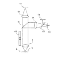
図5は、従来技術の自動合焦点装置を備えた光学顕微鏡の概略の構成を説明するための図である。図5において、62 は光学顕微鏡で観察する試料、61 は、試料 62 を載置する試料台、63 は、光学顕微鏡を構成する対物レンズ、64 は、光学顕微鏡を構成する結像レンズ、65 は、結像レンズ 64 の結像面位置、66 は、試料台 61 を上下に移動させる駆動機構部、67 は、光学顕微鏡の光路中に設けたハーフミラー、68 は、ハーフミラー 67 で反射した光を結像する合焦点用結像レンズ、70 は、合焦点用結像レンズ 68 の結像面位置より前ピン位置に設けた光電変換素子、69 は、合焦点用結像レンズ 68 の光路中に設けたハーフミラー、71 は、ハーフミラー 69 で反射した合焦点用結像レンズ 68 の結像面位置より後ピン位置に設けた光電変換素子を示す。
FIG. 5 is a diagram for explaining a schematic configuration of an optical microscope provided with a conventional automatic focusing device. In FIG. 5, 62 is a sample observed with an optical microscope, 61 is a sample stage on which the sample 62 is placed, 63 is an objective lens constituting the optical microscope, 64 is an imaging lens constituting the optical microscope, and 65 is The imaging surface position of the
図5を使用し、従来技術による自動合焦点装置を備えた光学顕微鏡の例をいくつか説明する。
光学顕微鏡は、試料台 61 上に載置した試料 62 を、対物レンズ 63 の焦点位置に設定し、試料 62 の所望の光学像を結像レンズ 64 による結像面位置 65 に結像して観察する。このような光学顕微鏡において、結像レンズ 64 による結像面位置 65 に、光電変換装置(図示していない。)を配置し、光電変換装置から、試料 62 の所望光学像を撮像した映像信号を出力する観察システムまたは測定システムあるいは検査システムあるいは加工システムがある。光電変換装置は例えば、テレビカメラ等の撮像装置である。
Several examples of optical microscopes equipped with a conventional automatic focusing device will be described with reference to FIG.
In the optical microscope, the sample 62 placed on the sample stage 61 is set at the focal position of the objective lens 63, and a desired optical image of the sample 62 is imaged at the
光電変換装置から出力された映像信号は、例えばプロセス装置(図示していない。)に与えられる。プロセス装置は、入力された映像信号から微分成分を検出し、検出した微分成分に応じた出力信号を生成し、試料台 61 を上下に移動させる駆動機構部 66 に出力する。駆動機構部 66 は、プロセス装置で検出される微分成分が最大出力となるように、微分成分に応じた出力信号に基づいて試料 62 が載置された試料台 61 を上下に駆動し、試料 62 と対物レンズ 63 の相対距離を調整する。そして、プロセス装置で検出される微分成分が最大出力となる位置を、合焦点位置とする。このように、試料 62 と対物レンズ 63 の相対距離が、プロセス装置で検出される微分成分が最大出力となる位置に制御する手段を有する自動合焦点装置を備えた光学顕微鏡がある(特許文献1、特許文献2参照。)。
The video signal output from the photoelectric conversion device is given to, for example, a process device (not shown). The process device detects a differential component from the input video signal, generates an output signal corresponding to the detected differential component, and outputs the output signal to the
しかし、前記のような自動合焦点装置を備えた光学顕微鏡は、光学顕微鏡の結像面位置 65 に配置した光電変換装置により光電変換された映像信号の微分成分を検出するものであるため、合焦点を行なうときの映像信号から微分成分が検出されないと合焦点は不可能であり、合焦点は、試料 62 に段差や輝度変化があり、明確な輪郭を有する試料 62 に限られることになる。しかしながら、試料 62 は、段差や輝度変化があり、輪郭が明確なものばかりとは限らないため、上記自動合焦点装置を備えた光学顕微鏡の欠点を補う手段として、輪郭が明確でない試料 62 上に、輝度変化のあるパターンを投影し、疑似輪郭を常に形成して、疑似輪郭を含む映像信号から微分成分を検出する手段を有する自動合焦点装置を備えた光学顕微鏡がある(特許文献3参照。)。
However, an optical microscope equipped with an automatic focusing device as described above detects the differential component of the video signal photoelectrically converted by the photoelectric conversion device arranged at the
上記自動合焦点装置を備えた光学顕微鏡は、一度に光学顕微鏡の光軸方向上の1点の微分成分を検出する。光軸方向上の複数点の微分成分は、試料台 61 を駆動部 66 で光軸方向上に動かしながら得られる。得られた複数の微分成分のなかで最大微分成分を有する試料 62 と対物レンズ 63 の相対距離を合焦点位置として制御する手段を有する自動合焦点装置を備えた光学顕微鏡である。したがって、光軸方向上の複数点の微分成分を調べるのに、検出時間と駆動時間を必要とし、迅速に合焦点検出をすることができないという問題がある。
An optical microscope equipped with the automatic focusing device detects a differential component at one point on the optical axis direction of the optical microscope at a time. The differential components at a plurality of points in the optical axis direction are obtained by moving the sample stage 61 in the optical axis direction by the
さらに、従来技術による合焦点方向を検出する手段を有する自動合焦点装置を備えた光学顕微鏡を、図5を使用して説明をする。
光学顕微鏡の光路、詳しくは、対物レンズ 63 から結像レンズ 64 への光路中にハーフミラー 67 を設置し、ハーフミラー 67 による反射光を合焦点用結像レンズ 68 により結像させる。合焦点用結像レンズ 68 による結像面位置より前ピン位置に前ピンセンサとして光電変換素子 70 を設け、合焦点用結像レンズ 68 から光電変換素子 70 への光路中にハーフミラー 69 を設置し、ハーフミラー 69 により反射した合焦点用結像レンズ 68 による結像面位置より後ピン位置に後ピンセンサとして光電変換素子 71 を設ける。
Furthermore, an optical microscope equipped with an automatic focusing device having means for detecting a focusing direction according to the prior art will be described with reference to FIG.
A
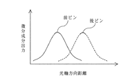
合焦点用結像レンズ 68 の結像面位置の前後に光電変換素子 70 、71 をそれぞれ配置し、図6に示すような前ピン信号、後ピン信号を得て、その差出力に応じて駆動機構部 66 を駆動し、試料台 61 を上下に移動させ、合焦点位置を得る自動合焦点装置を備えた光学顕微鏡がある(特許文献3参照。)。
前ピン信号と後ピン信号の微分成分出力が同じになる光軸方向距離を合焦点位置とする手段であり、前ピン位置と後ピン位置の結像は両者共に合焦点でなくボケているため、一般的にボケ方式と言われている。
This is a means for setting the distance in the optical axis direction where the differential component output of the front pin signal and the rear pin signal is the same as the in-focus position, and the images at the front pin position and the rear pin position are both out of focus but not in focus. Generally, it is said to be out of focus.
従来技術による自動合焦点装置を備えた光学顕微鏡においては、試料の観察したい場所の映像信号(例えば、二次元 CCD )から微分成分を検出し、合焦点となるように光学顕微鏡全体を移動制御するので、高精度であるが、移動時の振動吸収時間や映像信号を取得する時間(二次元 CCD の撮像時間)が必要で、総合で約3秒と合焦点に時間がかかるという欠点があった。
また、試料にパターンを投影する従来技術では、試料の輪郭と投影させたパターンの輪郭とが干渉し、観察に悪影響を与えるという欠点があった。
さらに、前ピンと後ピンによる制御であるため光軸上の2点での制御となり、複雑な形状を有し、焦点面が複数の試料に対しては、完全な制御ができないという欠点があった。
本発明の目的は、上記のような欠点を除去し、焦点面が複数存在する凹凸のある試料や輪郭が明確でない試料でも合焦点が可能で、迅速に合焦点可能な合焦点方法及び装置を提供することにある。
In an optical microscope equipped with a conventional automatic focusing device, a differential component is detected from a video signal (for example, a two-dimensional CCD) at a location where a sample is to be observed, and movement of the entire optical microscope is controlled so as to be in focus. Therefore, although it is highly accurate, it takes time to absorb vibration during movement and time to acquire video signals (two-dimensional CCD imaging time), and it takes about 3 seconds in total to take time to focus. .
Further, the conventional technique for projecting a pattern onto a sample has a drawback in that the outline of the sample interferes with the outline of the projected pattern, which adversely affects observation.
Furthermore, since the control is performed by the front pin and the rear pin, the control is performed at two points on the optical axis, and there is a disadvantage that complete control cannot be performed for a sample having a complicated shape and a focal plane. .
An object of the present invention is to provide an in-focus method and apparatus that eliminates the above-described drawbacks and can perform in-focus even with an uneven sample having a plurality of focal planes or a sample with unclear contours, and can be focused quickly. It is to provide.
上記の目的を達成するため、本発明の合焦点方法は、レーザダイオード等によるレーザスポット光からレーザスリット光を作り、レーザスリット光を試料の表面に投射し、試料から反射したレーザスリット光をハーフミラーを介して光軸に垂直に設けたラインセンサ上に結像し、ラインセンサを光軸方向に移動させ、移動距離とラインサンサ映像の高周波成分の量を特性化し、ラインサンサ映像の高周波成分の量が最大となる移動距離を検出して、最大の焦点位置を知ることができる合焦点方法を提供することを目的とする。 In order to achieve the above object, the focusing method of the present invention creates a laser slit light from a laser spot light by a laser diode or the like, projects the laser slit light on the surface of the sample, and half the laser slit light reflected from the sample. An image is formed on a line sensor provided perpendicular to the optical axis via a mirror, the line sensor is moved in the optical axis direction, the moving distance and the amount of high-frequency component of the line sensor image are characterized, and the amount of high-frequency component of the line sensor image An object of the present invention is to provide a focusing method capable of detecting the maximum moving position by detecting the moving distance that maximizes.
また本発明の合焦点装置は、少なくとも、観察する試料に焦点を結ぶように設けられた対物レンズと、対物レンズからの光の結像を所定の結像面位置に結ぶように設けられた結像レンズとを備えた光学顕微鏡であって、少なくとも、試料を載置し水平方向および垂直方向に移動可能な試料台と、入力される合焦点検出信号に応じて試料台と垂直方向に光学顕微鏡を移動させる駆動機構部とからなる自動合焦点装置において、試料台に載置された試料にスリット状のレーザ光を投射する手段と、試料から反射するスリット光を反射するための光学顕微鏡の光路中に設けたハーフミラーと、ハーフミラーからの反射光の結像を、対物レンズの焦点と共役位置に結ぶ合焦点用結像レンズと、合焦点用結像レンズの結像点において、光軸に対し垂直に設けた複数の光電変換素子からなるラインセンサと、ラインセンサを光軸方向に周期的に駆動するラインセンサ移動部を有し、ラインセンサ移動によって入射スリット光の高周波成分が最大となる前記ラインセンサ移動の位置を検出し、該ラインセンサの位置までの光路長とあらかじめ設定した焦点位置までの光路長との差を得て合焦点位置情報とし、その合焦点位置情報により、光学顕微鏡を試料台に対し、垂直方向に移動させるものである。 The focusing apparatus of the present invention includes at least an objective lens provided to focus on the sample to be observed, and a connection provided so as to connect the image of light from the objective lens to a predetermined imaging plane position. An optical microscope having an image lens, at least a sample stage on which a sample can be placed and moved in a horizontal direction and a vertical direction, and an optical microscope perpendicular to the sample stage in accordance with an input focus detection signal In the automatic focusing device comprising a drive mechanism unit for moving the optical microscope, means for projecting slit-shaped laser light onto the sample placed on the sample stage, and the optical path of the optical microscope for reflecting the slit light reflected from the sample An optical axis at the focal point of the in-focus image forming lens and the in-focus image forming lens that connects the image of the reflected light from the half mirror to the focal point and the conjugate position of the objective lens. Perpendicular to The line sensor movement having a line sensor composed of a plurality of photoelectric conversion elements and a line sensor moving unit that periodically drives the line sensor in the optical axis direction, and the high frequency component of the incident slit light is maximized by the line sensor movement. The position of the optical sensor is detected, and the difference between the optical path length to the position of the line sensor and the optical path length to the preset focal position is obtained as in-focus position information. On the other hand, it is moved in the vertical direction.
また、本発明の合焦点装置を備えた光学顕微鏡は、対物レンズの倍率の切換えに応じてラインセンサ移動範囲を変化させる手段を有し、切換えた対物レンズの倍率に適した合焦点検出信号を得て、試料台に対して垂直方向に移動させるものである。
また、本発明の自動合焦点装置を備えた光学顕微鏡は、試料にレーザ光を投射する手段が、少なくとも、レーザ発光源と、レーザ発光源で発光したレーザ光の発光束を拡大するビームエキスパンダと、スリット光生成のための通過板、スリット光を試料へ投射するように光学顕微鏡の光路中に設けられたハーフミラーとを有するものである。
The optical microscope equipped with the focusing device of the present invention has means for changing the line sensor moving range in accordance with the switching of the magnification of the objective lens, and outputs a focusing detection signal suitable for the switched magnification of the objective lens. Obtained and moved in a direction perpendicular to the sample stage.
Further, the optical microscope equipped with the automatic focusing device of the present invention includes a beam expander in which the means for projecting the laser beam onto the sample expands at least the laser emission source and the emission bundle of the laser beam emitted from the laser emission source. And a passage plate for generating slit light and a half mirror provided in the optical path of the optical microscope so as to project the slit light onto the sample.
また、本発明の合焦点位置検出装置は、試料を観察するための対物レンズと結像レンズを有する光学顕微鏡と、光学顕微鏡に設けられた合焦点位置検出装置であって、スリット光発生源と、スリット光発生源から出力されるスリット光を、第1の分岐手段により試料に照射し、試料からの反射光を光学顕微鏡に入射する光像を分岐する第1の分岐手段と、第1の分岐手段によって分岐された光像を顕微鏡の結像面位置と略共焦点位置に原点位置が設定されたラインセンサと、ラインセンサの位置を顕微鏡の結像面位置を含む複数の焦点距離範囲内を所定の周期で移動させるための移動手段と、ラインセンサが取得した複数の焦点距離範囲内の輝度レベルを元に顕微鏡の合焦点位置を検出する処理手段とを備えたことを特徴とする。 The in-focus position detection apparatus of the present invention is an optical microscope having an objective lens and an imaging lens for observing a sample, and an in-focus position detection apparatus provided in the optical microscope, including a slit light generation source The first branching means for irradiating the sample with the slit light output from the slit light generation source by the first branching means and for branching the light image incident on the optical microscope by the reflected light from the sample; The optical sensor branched by the branching means is a line sensor in which the origin position is set substantially confocal with the imaging plane position of the microscope, and the position of the line sensor is within a plurality of focal length ranges including the imaging plane position of the microscope. And a processing means for detecting the in-focus position of the microscope based on luminance levels within a plurality of focal length ranges acquired by the line sensor.
以上のように本発明によれば、レーザダイオード等によるレーザスリット光を試料の表面に投射し、試料から反射したスリット光をラインセンサ上に結像し、ラインセンサの映像の高周波成分から焦点深度を探すので、凹凸のある試料の平均的位置に合焦点が可能となる。かつ迅速に、合焦点が可能となる。
また、共焦点位置にある対物レンズと試料観察面位置と合焦点位置検出用ラインセンサ位置がそれらの取付部材の熱膨張をなくしたことにより周囲温度に影響されない自動合焦点装置を備えた光学顕微鏡を提供することができる。
As described above, according to the present invention, laser slit light from a laser diode or the like is projected onto the surface of the sample, and the slit light reflected from the sample is imaged on the line sensor. Therefore, it is possible to focus on the average position of the uneven sample. And it is possible to focus quickly.
In addition, an optical microscope provided with an automatic focusing device in which the objective lens at the confocal position, the position of the sample observation surface, and the line sensor position for detecting the focusing position are not affected by the ambient temperature by eliminating the thermal expansion of their mounting members. Can be provided.
本発明の一実施形態は、顕微鏡焦点内に試料を設定し、観察のため水平方向に試料を動かした場合、試料の凹凸に対しても、常に迅速に合焦点となるように追従する合焦点装置を備えた光学顕微鏡に関するものである。
以下、本発明の実施の形態について説明する。
In one embodiment of the present invention, when a sample is set within the microscope focus and the sample is moved in the horizontal direction for observation, the focal point always follows the unevenness of the sample so that the focal point is always quickly focused. The present invention relates to an optical microscope provided with the apparatus.
Embodiments of the present invention will be described below.
本発明の一実施例を、図1〜図4を使用して説明する。図1は、本発明の合焦点装置を備えた光学顕微鏡の概略の構成を示す図である。図1において、2 は光学顕微鏡で観察する試料、1 は試料 2 を載置して水平および垂直方向へ移動可能な試料台、3 は光学顕微鏡を構成する対物レンズ、4 は光学顕微鏡を構成する結像レンズ、5 は結像レンズ 4 の結像面位置、6 は入力される合焦点検出信号に応じて試料台 1 を上下に移動させる駆動機構部、7 は光学顕微鏡の光路中に設けたダイクロミラー、8 は反射ミラー、9 はラインセンサ用結像レンズ、10 はラインセンサ用結像レンズ 9 の結像面位置に設けた複数の光電変換素子からなるラインセンサ、15 はラインセンサ 10 を光軸方向に移動させるラインセンサ移動部、11 はスリット光発光源、12 はスリット光発光源 11 で発光したレーザ光の発光束を拡大するビームエキスパンダ、13 はスリット光を生成するスリット光通過板、14 はスリット光通過板 13 でスリット化したスリット光を反射するハーフミラー、16 は合焦点位置を検出する検出部である。
An embodiment of the present invention will be described with reference to FIGS. FIG. 1 is a diagram showing a schematic configuration of an optical microscope provided with a focusing device of the present invention. In FIG. 1, 2 is a sample to be observed with an optical microscope, 1 is a sample stage on which a sample 2 is placed and can be moved horizontally and vertically, 3 is an objective lens constituting the optical microscope, and 4 is an optical microscope. The imaging lens, 5 is the imaging plane position of the
図1を使用し、本発明による自動合焦点装置を備えた光学顕微鏡を説明する。試料台 1 上に載置した試料 2 を、光学顕微鏡の対物レンズ 3 の焦点位置付近に設定し、試料 2 の所望の場所の光学像を結像レンズ 4 による結像面位置 5 に結像させ、結像面位置 5 に、光電変換装置(図示していない。)を配置し観察する。光電変換装置は、例えば、テレビカメラ等の撮像装置である。
スリット光発光源 11 から出力されるレーザ光はビームエキスパンダ 12 に到達し、ビームエキスパンダ 12 は発光束を拡大して出力する。スリット光発光源 11 は、例えば、レーザダイオードである。発光束を拡大されたレーザ光は、スリット生成遮蔽板 13 を通ってスリット光となり、ハーフミラー 14 で反射し、対物レンズ 3 により集光される。集光されたスリット光は、試料 2 の表面に投射される。
An optical microscope equipped with an automatic focusing device according to the present invention will be described with reference to FIG. The sample 2 placed on the sample table 1 is set near the focal position of the objective lens 3 of the optical microscope, and an optical image of the desired location of the sample 2 is formed on the
The laser light output from the slit
試料 2 の表面に投射されたスリット光は、試料 2 の表面で反射され、反射光が対物レンズ 3 を通ってハーフミラー 14 に到達する。ハーフミラー 14 は、到達した光の一部をダイクロミラー 7 に分岐させる。ダイクロミラー 7 は、到達した光を反射ミラー 8 に出力する。ダイクロミラー 7 で反射され、反射ミラー 8 で更に反射されたスリット光は、ラインセンサ用結像レンズ 9 に入射し、ラインセンサ 10 に投影される。
The slit light projected on the surface of the sample 2 is reflected on the surface of the sample 2, and the reflected light passes through the objective lens 3 and reaches the
ラインセンサ 10 の原点位置は、対物レンズ 3 及び結像面位置 5 と共焦点位置に配置されている。対物レンズ 3 の合焦点位置に、試料 2 があるとき、ラインセンサ 10 及び結像面位置 5 に投影される像が合焦点画像となる。
対物レンズ 3 と試料 2 が近づいたときには、ラインセンサ 10 及び結像面位置 5 に投影される像がぼける。そして、ラインセンサ 10 を光軸方向に遠ざけた位置に、合焦点画像がずれる。
対物レンズ 3 と試料 2 が離れたときには、ラインセンサ 10 及び結像面位置 5 に投影される像がぼける。そして、ラインセンサ 10 を光軸方向に近づけた位置に、合焦点画像がずれる。
The origin position of the
When the objective lens 3 and the sample 2 are close to each other, the image projected on the
When the objective lens 3 and the sample 2 are separated from each other, the image projected on the
すなわち、ラインセンサ 10 を光軸方向に移動させることにより、対物レンズ 3 と試料 2 の位置関係がわかる。
ランセンサ 10 は、光軸方向に移動できるように設けられ、一定の周期で一定範囲内で光軸方向に振動する。
例えば、対物レンズ 3 の倍率が 100 倍の時には、焦点位置を中心(原点 0 μm )とし、±10 μm の範囲を 100 Hz で光軸方向に振動する。
例えば、対物レンズ 3 の倍率が 10 倍の時は、焦点位置を中心とし、±100 μm の範囲を 100 Hz で光軸方向に振動する。
That is, the positional relationship between the objective lens 3 and the sample 2 can be determined by moving the
The
For example, when the magnification of the objective lens 3 is 100 times, the focal position is the center (the origin is 0 μm), and the range of ± 10 μm vibrates in the direction of the optical axis at 100 Hz.
For example, when the magnification of the objective lens 3 is 10 times, it vibrates in the direction of the optical axis at 100 Hz in the range of ± 100 μm centered on the focal position.
対物レンズ 3 として 10 倍の倍率のレンズを使用する場合を例にとって、図1と図2によって合焦点位置の検出方法について更に説明する。図2は、本発明の自動合焦点装置を備えた光学顕微鏡において、一定周期で振動するラインセンサ移動部とラインセンサタイミングチャートの対物レンズ 3 に 10 倍時の粗動作の一実施例を説明する図である。
図2(a) 〜(d) において、横軸は時間である。また、図2(a) はラインセンサ 10 の光軸方向の移動量を示す図で、縦軸が原点( 0 μm )を中心とした長さで、ライン 151 が移動量を示す。また、図2(b) はラインセンサ 10 の走査波形 152 を示す図で、縦軸が信号レベルを示す。また、図2(c) はラインセンサ 10 が取得した映像波形 153 を示す図で、縦軸が輝度レベルを示す。また、図2(d) はラインセンサ 10 の映像波形 153 の高周波成分 154 を示す図で、縦軸がレベルを示す。
Taking as an example the case where a 10 × magnification lens is used as the objective lens 3, the method for detecting the in-focus position will be further described with reference to FIGS. 1 and 2. FIG. 2 is a diagram illustrating an embodiment of a coarse operation at 10 times on a line sensor moving unit that vibrates at a constant period and an objective lens 3 of a line sensor timing chart in an optical microscope equipped with the automatic focusing device of the present invention. FIG.
2 (a) to 2 (d), the horizontal axis represents time. FIG. 2 (a) shows the amount of movement of the
検出部 16 は、ラインセンサ移動部 15 を、ライン 151 で示すように 10 ms の周期で振動させ、ラインセンサ 10 を光軸方向に−100 μm から+100 μm 迄の間で移動させる。
ラインセンサ 10 の走査周期は、走査波形 152 に示すように 0.5 ms であり、映像波形 153 に示すように 0.5 ms でスリット光の映像を取得する。取得された映像は検出部 16(図1参照)に与えられる。
映像波形 153 のような映像では、例えば、高周波成分 154 に示すような波形の高周波成分が得られる。
したがって、この高周波成分 154 の値が最大となる位置が合焦点位置であり、移動量 0 μm から −60 〜−50 μm の間に合焦点位置があることがわかる。検出部 16 は、この情報をもとに、光学顕微鏡の対物レンズ 3 と試料 2 との距離を調整するために駆動機構 6 を動かす。
The
The scanning cycle of the
In a video such as the
Therefore, it can be seen that the position where the value of the high-frequency component 154 is the maximum is the in-focus position, and the in-focus position is between −60 to −50 μm from the movement amount 0 μm. Based on this information, the
次に、本発明の一実施形態では、図2で説明したように粗動作によって駆動機構 6 を移動した後、以下の図3の説明のように微動作を行う。図3は、本発明の自動合焦点装置を備えた光学顕微鏡において、一定周期で振動するラインセンサ移動部とラインセンサタイミングチャートの対物レンズ 3 に 10 倍時の微動作の一実施例を説明する図である。
図3(a) (b) (c) (d) は、図2と同様に、(a) はラインセンサ 10 の光軸方向の移動量を波形 161 で示す図、(b) はラインセンサ 10 の走査波形 162 を示す図、(c) はラインセンサ 10 が取得した映像波形 163 を示す図、及び (d) はラインセンサ 10 の映像波形 163 の高周波成分 164 を示す図である。
Next, in one embodiment of the present invention, the drive mechanism 6 is moved by the coarse operation as described in FIG. 2, and then the fine operation is performed as described in FIG. 3 below. FIG. 3 is a diagram illustrating an example of a fine operation at 10 times on a line sensor moving unit that vibrates at a constant period and an objective lens 3 of a line sensor timing chart in an optical microscope equipped with the automatic focusing device of the present invention. FIG.
3 (a), (b), (c), and (d) are the same as in FIG. 2, (a) is a diagram showing the amount of movement of the
検出部 16 は、まずラインセンサ移動部 15 を、波形 151 で示すように 10 ms の周期で振動させ、ラインセンサ 10 を光軸方向に−10 μm から+10 μm 迄の間で移動させる。
ラインセンサ 10 の走査周期は、走査波形 162 に示すように 0.5 ms で、映像波形 163 に示すように 0.5 ms でスリット光の映像を取得する。
映像波形 163 のような映像では、例えば、高周波成分 164 に示すような波形の高周波成分が得られる。
したがって、この高周波成分 164 の値が最大となる位置が合焦点位置であり、移動量 0μm から 60 〜 1μm の間が合焦点位置があることがわかる。この情報をもとに、検出部 16 は、光学顕微鏡の対物レンズ 3 と試料 2 との距離を調整するために駆動機構 6 を動かす。これによって、対物レンズ 3 の倍率が 10 倍のときの焦点深度 1μm 以内に、試料 2 と対物レンズ 3 との間の距離が定まる。
First, the
The scanning cycle of the
In a video such as the
Therefore, it can be seen that the position where the value of the high-
同様に、対物レンズ 3 として 100 倍の倍率のレンズを使用する場合には、粗動作時には、ラインセンサ 10 を光軸方向に、焦点位置を中心として±10 μm の範囲を 100 Hz で光軸方向に振動する。そして微動作時には、ラインセンサ 10 を光軸方向に、焦点位置を中心として±1 μm の範囲を 100 Hz で光軸方向に振動する。
そのほか、対物レンズの倍率に応じて粗動作及び微動作の振動範囲を変更する。
Similarly, when a lens with a magnification of 100 times is used as the objective lens 3, during coarse operation, the
In addition, the vibration range of the coarse operation and the fine operation is changed according to the magnification of the objective lens.
次に、図8を用いて、ラインセンサ 10 を光軸方向に振動させる機構について説明する。図8は、本発明のラインセンサを光軸方向に移動する機構の一実施例を説明するための図である。
801 はシーソー台、802 は支点、803 はピエゾスタック、804 はバネ、805 は土台、806 は支柱である。
図8において、ラインセンサ 10 は、シ−ソー台 801 に取付けられ、支点 802 に対してラインセンサ 10 と反対側にピエゾスタック 803 及びバネ 804 が取付けられている。
土台 805 に支柱 806 を配置し、支点 802 でシーソー台 801 を支える。ピエゾスタック 803 を土台 805 とシーソー台 801 の間に挟み、土台 805 とシーソー台 801 の間をバネ 804 でつなぎ、バネ 804 でピエゾスタック 803 を固定する。
Next, a mechanism for vibrating the
801 is a seesaw base, 802 is a fulcrum, 803 is a piezo stack, 804 is a spring, 805 is a base, and 806 is a support.
In FIG. 8, the
The
ピエゾスタック 803 は、その両端に電圧 0 V 印加したときに、土台 805 とシーソー台 801 の間の長さが 35.0 mm で、電圧 100 V を印加したときに、長さ 35.333 mm となる。従って、電圧 0 V 〜 100 V の間で、長さが 33.3 μm 変化する。その間の長さは、電圧にほぼ比例配分される。
ピエゾスタック 803 と支点 803 の距離を S とし、支点 803 とラインセンサ 10 の距離を 6S とすることで、ラインセンサ 10 は、光軸方向(矢印方向)に約 200 μm(= 33.3 μm × 6 ) 変化する。
The
By setting the distance between the
ピエゾスタック 803 、支点 802 及びシーソー台 801 は 100 Hz の振動に対応できる機構なので、ピエゾスタック 803 に 0 〜 100 V の電圧を 100 Hz の周波数で変化させることにより、ラインセンサ 10 は、光軸方向に 0 〜 200 μm 振動する。
The
ピエゾスタック 803 に電圧 50 V を印加した位置、すなわちラインセンサ 10 が 100 μm の位置を共焦点位置 0 に設定することで、ラインセンサ 10 は焦点方向に±約 100 μm 光軸方向に振動する。
By setting the position where the voltage 50 V is applied to the
図4は、スリット光とラインセンサ 10 と試料 2 との関係を説明するための図である。また、図4(b) (c) は、描画されたライン 102′を観察することを目的とした場合の照射されるスリット光 103 と描画されたライン 102′との関係を示す図の例である。
図4(a) において、スリット光を試料 2 に照射したとき、試料 2 を反射したスリット光の像 102 は、ラインセンサ 10 の受光面 101 に図2(a) に示すように投影される。
FIG. 4 is a diagram for explaining the relationship among the slit light, the
4A, when the sample 2 is irradiated with the slit light, the slit
図4(b) において、スリット光 103 を図4(b) のように試料 2 の描画されたライン 102′に略 1/4πラジアンになるようにして試料 2 に照射する。
描画されたライン 102′の焦点位置と描画されたライン 102′の周辺の焦点位置の平均が検出できるようにする。
しかし、図4(c) に示すように描画されたライン 102′とラインセンサ 10 の受光面 101 が平行になるように設定すると、描画されたライン 102′の焦点位置が検出できず、描画されたライン 102′周辺だけの焦点位置検出となってしまう。従って、本発明では、図4(b) に示すように、描画されたライン 102′に略 1/4πラジアンになるようにして試料 2 にスリット光を照射することで、描画されたライン 102′周辺だけの焦点位置検出となってしまうことを避ける。
In FIG. 4B, the
The average of the focal position of the drawn line 102 'and the focal position around the drawn line 102' can be detected.
However, if the drawn line 102 'and the
また、本発明の一実施例では、周囲温度の影響で、共焦点位置にある対物レンズと試料観察面(撮像装置受光面)位置と合焦点位置検出用ラインセンサ位置がそれらの取付部材の熱膨張で狂わないようにそれらの取付部材を、熱膨張係数がほぼゼロの材質のもの(例えば、ノビナイト)を使用する。 In one embodiment of the present invention, due to the influence of ambient temperature, the objective lens at the confocal position, the position of the sample observation surface (light receiving surface of the imaging device), and the position of the line sensor for detecting the in-focus position are the heat of the mounting members. Those mounting members are made of a material having a substantially zero thermal expansion coefficient (for example, novinite) so as not to be distorted by expansion.
次に、上述したような自動合焦点顕微鏡の応用システムについて、図7を用いて説明する。
光学顕微鏡を用いたシステムは、例えば、LCD( Liquid Crystal Display :液晶ディスプレイ)基板や PDP( Plasma Display Panel )等の FPD( Flat Panel Display )、及び、半導体ウェハ等の各種基板、並びに、それらのリソグラフィに使用するマスク基板を測定または検査あるいは加工する場合に使用される。それらの対象の基板は、例えば、蒸着やエッチング等の膜製造技術を用いて製作される。図7は、上記のような基板の線幅を測定するための従来の線幅測定システムの構成の一例を示すブロック図である。
Next, an application system of the automatic focusing microscope as described above will be described with reference to FIG.
A system using an optical microscope includes, for example, an LCD (Liquid Crystal Display) substrate, an FPD (Flat Panel Display) such as a PDP (Plasma Display Panel), various substrates such as a semiconductor wafer, and lithography thereof. It is used when measuring, inspecting, or processing a mask substrate used for the above. These target substrates are manufactured using a film manufacturing technique such as vapor deposition or etching, for example. FIG. 7 is a block diagram showing an example of the configuration of a conventional line width measurement system for measuring the line width of the substrate as described above.
LCD 基板等の検査対象物 701 は、基板クランプ台 702 でその裏面を吸着されることによって固定されている。尚、基板クランプ台 702 は、図示しない真空ポンプ等で検査対象物 701 の裏面を吸着する、所謂真空チャックの構造になっている。基板クランプ台 702 は、除振台 705 上に配置された Y 軸移動ステージ 704 と X 軸移動ステージ 703 の上に設けられている。検査対象物 701 は、X 軸移動ステージ 703 と Y 軸移動ステージ 704 とをそれぞれ、X 軸方向、Y 軸方向に動かすことによって、X 、Y 平面内を移動でき、検査対象物 701 内の所定の位置を光学顕微鏡 708 で観察することができる。所定の位置とは、例えば、配線パターンが形成された所定の位置の線幅を測定し、製品または半製品の良否を判定するもので、前もって定められる位置である。
An
X 軸移動ステージ 703 と Y 軸移動ステージ 704 は、それぞれ、測定制御部 716 によって手動または自動的に操作され、所定の位置が光学顕微鏡 708 の視野に入るように制御される。検査対象物 701 の検査項目は、例えば、自動線幅測定装置の場合は、それらの基板上に形成された電極パターンや配線パターンの線幅や間隔の測定及び、それら電極パターンや配線パターン間のずれ量等である。
The
照明光源 706 は、ライトガイド 709 で光を光学顕微鏡 708 に導入する。導入された光は検査対物レンズ 711 を介し検査対象物 701 に投射される。投射された光は検査対象物 701 で反射し、その反射光が検査対物レンズ 711 、中間レンズ 714 を介し、カメラ 715 に入射される。カメラ 715 は、入射光を電気信号に変換して測定制御部 716 に出力する。なおこの光は、可視光、赤外線、紫外線、等であり、カメラ 715 はこれらの光を電気信号に変換できる CCD( Charge Coupled Device )等の撮像素子である。
The
変倍機構(レボルバ)710 は、目的に応じて検査対物レンズ 711 を予備アライメント用対物レンズ 712 と交換できるような機構になっている。光軸( Z 軸)移動ステージ 713 は、検査対物レンズ 711 の焦点距離を合焦点位置に調節するために、検査対物レンズ 711 を装着した光学顕微鏡 708 全体を光軸( Z 軸)方向に移動するためのものである。中間レンズ 714 は、検査対物レンズ 711 からの像を拡大してカメラ 715 に投影するものである。カメラ 715 が撮像した映像は、測定制御部(検査制御部)716 内の画像処理部 761 に入力される。
The zooming mechanism (revolver) 710 is a mechanism that can replace the inspection
光軸( Z 軸)移動制御部 762 は、検査対物レンズ 711 の焦点距離を適正に調節するために、検査対物レンズ 711 を装着した光学顕微鏡 708 全体を光軸( Z 軸)方向に移動させるための焦点距離制御部である。尚、焦点距離制御部 762 は、画像処理部 761 からの信号に基づいてオートフォーカス制御する機能も有している。CPU 763 は、測定制御部(検査制御部)716 を制御するプログラムを有し、線幅測定装置を動かす。CPU 763 は、焦点距離制御部 762 、画像処理部 761 、XY 移動制御部 707 を制御するプログラムを有する。XY 移動制御部 707 内には、X 軸移動ステージ703 と Y 軸移動ステージ 704 を移動させる移動制御部 771 、基板クランプ台 702 上で基板 701 を固定する基板を押し当て制御部 772 、基板 1 の裏面を基板クランプ台 2 に吸着させる基板裏面吸着制御部 773 と基板 701 を基板搬送ハンド 718 から基板クランプ台 702 に受取るための基板受取りピン上下制御部 774 からなる。CRT 717 は、画像及び操作スイッチが表示されるモニタ画面であり、マウス等のポインティングデバイスを GUI( Graphical user interface )によって操作者が操作することができる。
検査対象物の基板 701 は、基板搬送ハンド 718 で搬送され、基板クランプ台 702 上に載置される。図3では、基板搬送ハンド 718 が左右(両矢印の方向)に動き、基板 701 を搬送する。
The optical axis (Z-axis)
The
図7で説明した測定制御部(検査制御部)716 が、図1〜図4によって説明した本発明の実施例において、合焦点検出のための処理部(検出部)を含んでも良いことは自明である。
また、本実施例では、焦点検出用のラインセンサの光軸を、光学顕微鏡の光軸と垂直の方向に設けたが、特別に垂直にする必要は無く、ラインセンサの光軸の方向にラインセンサが前後に振動するようにすれば良いことは自明である。
また、ラインセンサだけではなく、ラインセンサ用結像レンズの位置を同時にまたは別に振動させても良い。
また、ラインセンサではなく、エリアセンサであっても良い。
また、図1の実施例では、スリット光発生源 11 から出力されるスリット光がダイクロミラー 7 を介して直にハーフミラー 14 に入射し、試料 2 からの反射光はダイクロミラー 7 によって分岐されてラインセンサ 10 に入射されるようにしている。しかし、ラインセンサ 10 とスリット光発生源 11 の配置を上記と逆の配置にしても良いことは自明である。
It is obvious that the measurement control unit (inspection control unit) 716 described in FIG. 7 may include a processing unit (detection unit) for detecting a focal point in the embodiment of the present invention described with reference to FIGS. It is.
In this embodiment, the optical axis of the focus detection line sensor is provided in a direction perpendicular to the optical axis of the optical microscope. However, the optical axis of the line sensor is not required to be specially perpendicular to the line sensor. Obviously, the sensor should vibrate back and forth.
In addition to the line sensor, the position of the line sensor imaging lens may be vibrated simultaneously or separately.
Further, an area sensor may be used instead of the line sensor.
Further, in the embodiment of FIG. 1, the slit light output from the
1:試料台、 2:試料、 3:対物レンズ、 4:結像レンズ、 5:結像面位置、 6:駆動機構部、 7:ダイクロミラー、 8:反射ミラー、 9:ラインセンサ用結像レンズ、 10:ラインセンサ、 11:スリット光発光源、 12:ビームエキスパンダ、 13:スリット光通過板、 14:ハーフミラー、 15:ラインセンサ移動部、 16:検出部、 61:試料台、62:光学顕微鏡で観察する試料、 63:対物レンズ、 64:結像レンズ、 65:結像面位置、 66:駆動機構部、 67:ハーフミラー、 68:合焦点用結像レンズ、 69:ハーフミラー、 70,71:光電変換素子
1: sample stage, 2: sample, 3: objective lens, 4: imaging lens, 5: imaging surface position, 6: drive mechanism, 7: dichroic mirror, 8: reflection mirror, 9: imaging for line sensor Lens, 10: Line sensor, 11: Slit light emission source, 12: Beam expander, 13: Slit light passage plate, 14: Half mirror, 15: Line sensor moving unit, 16: Detection unit, 61: Sample stage, 62 : Sample to be observed with an optical microscope, 63: Objective lens, 64: Imaging lens, 65: Imaging plane position, 66: Drive mechanism, 67: Half mirror, 68: Imaging lens for focusing, 69: Half mirror , 70, 71: photoelectric conversion element
Claims (5)
上記試料から上記光学顕微鏡に入射する光像を分岐し、
該分岐された光像を複数の距離で結像し、
該複数の距離で結像した輝度をそれぞれ検出し、
該検出された輝度が所定の範囲内にある場合の距離を算出し、
該算出された距離に基づいて光学顕微鏡の合焦点位置を検出することを特徴とする合焦点位置検出方法。 An optical microscope for observing a sample, and a focusing position detection device provided in the optical microscope,
Branch the light image incident on the optical microscope from the sample,
Forming the branched light image at a plurality of distances;
Detect the brightness imaged at the plurality of distances,
Calculating a distance when the detected luminance is within a predetermined range;
A focused position detection method, comprising: detecting a focused position of an optical microscope based on the calculated distance.
上記光学顕微鏡の対物レンズの倍率に応じて、上記分岐された構造を結像する距離の範囲を変更することを特徴とする合焦点位置検出方法。 The in-focus position detection method according to claim 1,
An in-focus position detecting method, wherein a range of a distance for imaging the branched structure is changed according to a magnification of an objective lens of the optical microscope.
上記分岐された構造を結像する距離の変更を連続的に行い、
所定の周期に応じて上記距離の情報を取得することを特徴とする合焦点位置検出方法。 The in-focus position detection method according to claim 1 or 2,
Continuously changing the distance to image the branched structure,
An in-focus position detection method, wherein the distance information is acquired according to a predetermined period.
上記合焦点位置の検出を複数回行い、
検出の都度、前回の距離より、結像する距離の範囲を小さくすることを特徴とする合焦点位置検出方法。 The in-focus position detection method according to any one of claims 1 to 3,
The in-focus position is detected multiple times,
An in-focus position detection method characterized in that the range of the distance to be imaged is made smaller than the previous distance for each detection.
スリット光発生源と、
該スリット光発生源から出力されるスリット光を、上記第1の分岐手段により上記試料に照射し、上記試料からの反射光を上記光学顕微鏡に入射する光像を分岐する第1の分岐手段と、
該第1の分岐手段によって分岐された光像を上記顕微鏡の結像面位置と略共焦点位置に原点位置が設定されたラインセンサと、
該ラインセンサの位置を上記顕微鏡の結像面位置を含む複数の焦点距離範囲内を所定の周期で移動させるための移動手段と、
該ラインセンサが取得した該複数の焦点距離範囲内の輝度レベルを元に上記顕微鏡の合焦点位置を検出する処理手段とを備えたことを特徴とする合焦点位置検出装置。
An optical microscope having an objective lens and an imaging lens for observing a sample, and a focusing position detection device provided in the optical microscope,
A slit light source;
A first branching unit that irradiates the sample with slit light output from the slit light generation source by the first branching unit, and branches a light image incident on the optical microscope by reflected light from the sample; ,
A line sensor having an origin position set at a position substantially confocal with the imaging plane position of the microscope, and the optical image branched by the first branching unit;
Moving means for moving the position of the line sensor within a plurality of focal length ranges including the imaging plane position of the microscope with a predetermined period;
An in-focus position detection apparatus comprising: processing means for detecting an in-focus position of the microscope based on luminance levels within the plurality of focal length ranges acquired by the line sensor.
Priority Applications (1)
| Application Number | Priority Date | Filing Date | Title |
|---|---|---|---|
| JP2004007612A JP2005202092A (en) | 2004-01-15 | 2004-01-15 | Focusing point detecting method and optical microscope using the same |
Applications Claiming Priority (1)
| Application Number | Priority Date | Filing Date | Title |
|---|---|---|---|
| JP2004007612A JP2005202092A (en) | 2004-01-15 | 2004-01-15 | Focusing point detecting method and optical microscope using the same |
Publications (1)
| Publication Number | Publication Date |
|---|---|
| JP2005202092A true JP2005202092A (en) | 2005-07-28 |
Family
ID=34821189
Family Applications (1)
| Application Number | Title | Priority Date | Filing Date |
|---|---|---|---|
| JP2004007612A Pending JP2005202092A (en) | 2004-01-15 | 2004-01-15 | Focusing point detecting method and optical microscope using the same |
Country Status (1)
| Country | Link |
|---|---|
| JP (1) | JP2005202092A (en) |
Cited By (15)
| Publication number | Priority date | Publication date | Assignee | Title |
|---|---|---|---|---|
| JP2007232930A (en) * | 2006-02-28 | 2007-09-13 | Toshiba Corp | Focusing device and method |
| WO2011049608A2 (en) | 2009-10-19 | 2011-04-28 | Bioimagene, Inc. | Imaging system and techniques |
| JP2012506060A (en) * | 2008-10-14 | 2012-03-08 | サンフォード−バーナム メディカル リサーチ インスティテュート | Automated scanning cytometry using chromatic aberration for multi-plane image acquisition. |
| JP2013127581A (en) * | 2011-12-19 | 2013-06-27 | Hamamatsu Photonics Kk | Image acquisition device and focus method for image acquisition device |
| US20140204196A1 (en) * | 2011-09-09 | 2014-07-24 | Ventana Medical Systems, Inc. | Focus and imaging system and techniques using error signal |
| JP2015187748A (en) * | 2011-07-29 | 2015-10-29 | エフエフイーアイ リミティド | Method and device for image scanning |
| EP2916160A4 (en) * | 2012-10-31 | 2016-06-01 | Hamamatsu Photonics Kk | Image acquisition device and method for focusing image acquisition device |
| EP2916159A4 (en) * | 2012-10-31 | 2016-06-08 | Hamamatsu Photonics Kk | Image acquisition device and image acquisition method |
| US9860437B2 (en) | 2011-12-19 | 2018-01-02 | Hamamatsu Photonics K.K. | Image capturing apparatus and focusing method thereof |
| US9921392B2 (en) | 2011-12-19 | 2018-03-20 | Hamamatsu Photonics K.K. | Image capturing apparatus and focusing method thereof |
| US9971140B2 (en) | 2011-12-19 | 2018-05-15 | Hamamatsu Photonics K.K. | Image capturing apparatus and focusing method thereof |
| US10001622B2 (en) | 2011-10-25 | 2018-06-19 | Sanford Burnham Medical Research Institute | Multifunction autofocus system and method for automated microscopy |
| US10298833B2 (en) | 2011-12-19 | 2019-05-21 | Hamamatsu Photonics K.K. | Image capturing apparatus and focusing method thereof |
| CN114321840A (en) * | 2021-12-31 | 2022-04-12 | 广州市浩洋电子股份有限公司 | Optical focusing method of stage lamp and stage lamp optical system |
| CN114994896A (en) * | 2022-06-08 | 2022-09-02 | 合肥埃科光电科技股份有限公司 | Microscope automatic focusing system for micro-nano step sample and focusing method thereof |
-
2004
- 2004-01-15 JP JP2004007612A patent/JP2005202092A/en active Pending
Cited By (29)
| Publication number | Priority date | Publication date | Assignee | Title |
|---|---|---|---|---|
| JP2007232930A (en) * | 2006-02-28 | 2007-09-13 | Toshiba Corp | Focusing device and method |
| US8760756B2 (en) | 2008-10-14 | 2014-06-24 | Burnham Institute For Medical Research | Automated scanning cytometry using chromatic aberration for multiplanar image acquisition |
| JP2012506060A (en) * | 2008-10-14 | 2012-03-08 | サンフォード−バーナム メディカル リサーチ インスティテュート | Automated scanning cytometry using chromatic aberration for multi-plane image acquisition. |
| KR101420030B1 (en) | 2009-10-19 | 2014-07-15 | 벤타나 메디컬 시스템즈, 인코포레이티드 | Imaging system and techniques |
| US10061107B2 (en) | 2009-10-19 | 2018-08-28 | Ventana Medical Systems, Inc. | Method and device for slide scanning |
| JP2013508746A (en) * | 2009-10-19 | 2013-03-07 | ベンタナ メディカル システムズ, インコーポレイテッド | Imaging system and technique |
| US9575301B2 (en) | 2009-10-19 | 2017-02-21 | Ventana Medical Systems, Inc. | Device for a microscope stage |
| WO2011049608A2 (en) | 2009-10-19 | 2011-04-28 | Bioimagene, Inc. | Imaging system and techniques |
| CN104020553A (en) * | 2009-10-19 | 2014-09-03 | 文塔纳医疗系统公司 | Imaging system and techniques |
| EP2491452A4 (en) * | 2009-10-19 | 2015-03-11 | Ventana Med Syst Inc | Imaging system and techniques |
| US9036255B2 (en) | 2009-10-19 | 2015-05-19 | Ventana Medical Systems, Inc. | Method and device for slide caching |
| US20150153555A1 (en) * | 2009-10-19 | 2015-06-04 | Ventana Medical Systems, Inc. | Imaging system and techniques |
| JP2015187748A (en) * | 2011-07-29 | 2015-10-29 | エフエフイーアイ リミティド | Method and device for image scanning |
| US9903785B2 (en) | 2011-07-29 | 2018-02-27 | Ffei Limited | Method and apparatus for image scanning |
| US20140204196A1 (en) * | 2011-09-09 | 2014-07-24 | Ventana Medical Systems, Inc. | Focus and imaging system and techniques using error signal |
| US10001622B2 (en) | 2011-10-25 | 2018-06-19 | Sanford Burnham Medical Research Institute | Multifunction autofocus system and method for automated microscopy |
| JP2013127581A (en) * | 2011-12-19 | 2013-06-27 | Hamamatsu Photonics Kk | Image acquisition device and focus method for image acquisition device |
| US9921392B2 (en) | 2011-12-19 | 2018-03-20 | Hamamatsu Photonics K.K. | Image capturing apparatus and focusing method thereof |
| US9971140B2 (en) | 2011-12-19 | 2018-05-15 | Hamamatsu Photonics K.K. | Image capturing apparatus and focusing method thereof |
| US9860437B2 (en) | 2011-12-19 | 2018-01-02 | Hamamatsu Photonics K.K. | Image capturing apparatus and focusing method thereof |
| US10298833B2 (en) | 2011-12-19 | 2019-05-21 | Hamamatsu Photonics K.K. | Image capturing apparatus and focusing method thereof |
| US10571664B2 (en) | 2011-12-19 | 2020-02-25 | Hamamatsu Photonics K.K. | Image capturing apparatus and focusing method thereof |
| EP2916160A4 (en) * | 2012-10-31 | 2016-06-01 | Hamamatsu Photonics Kk | Image acquisition device and method for focusing image acquisition device |
| EP2916159A4 (en) * | 2012-10-31 | 2016-06-08 | Hamamatsu Photonics Kk | Image acquisition device and image acquisition method |
| EP3333614A3 (en) * | 2012-10-31 | 2018-09-05 | Hamamatsu Photonics K.K. | Image capturing apparatus and image capturing method |
| EP3333613A3 (en) * | 2012-10-31 | 2018-09-05 | Hamamatsu Photonics K.K. | Image capturing apparatus and image capturing method |
| CN114321840A (en) * | 2021-12-31 | 2022-04-12 | 广州市浩洋电子股份有限公司 | Optical focusing method of stage lamp and stage lamp optical system |
| CN114321840B (en) * | 2021-12-31 | 2023-08-29 | 广州市浩洋电子股份有限公司 | Stage lamp optical focusing method and stage lamp optical system |
| CN114994896A (en) * | 2022-06-08 | 2022-09-02 | 合肥埃科光电科技股份有限公司 | Microscope automatic focusing system for micro-nano step sample and focusing method thereof |
Similar Documents
| Publication | Publication Date | Title |
|---|---|---|
| TW472132B (en) | Focal point position control mechanism and method and apparatus and method for inspecting semiconductor wafer | |
| US9400176B2 (en) | Dynamic focus adjustment with optical height detection apparatus in electron beam system | |
| JP2005202092A (en) | Focusing point detecting method and optical microscope using the same | |
| KR20160013813A (en) | Auto-Focus system | |
| JP2001241940A (en) | Apparatus and method of measuring features on board | |
| JPH09266169A (en) | Exposure method | |
| TWI291546B (en) | Apparatus for inspecting a cut surface of a glass substrate | |
| JPH05264221A (en) | Device for detecting mark position for semiconductor exposure device and positioning deice for semiconductor exposure device using the same | |
| JP2011257303A (en) | Image acquisition device, defect correction device and image acquisition method | |
| JP2008300394A (en) | Substrate joining device and substrate joining method | |
| JPS58181005A (en) | Automatically focusing and measuring apparatus and method | |
| WO2018019277A1 (en) | Machine vision system for substrate alignment and alignment device | |
| JP6643328B2 (en) | Optical system for producing lithographic structures | |
| JP5134603B2 (en) | Light beam adjusting method and light beam adjusting apparatus | |
| JP5096852B2 (en) | Line width measuring apparatus and inspection method of line width measuring apparatus | |
| KR20210070909A (en) | Laser beam adjusting mechanism and laser machining apparatus | |
| JP5250395B2 (en) | Inspection device | |
| JP2003294419A (en) | Measuring instrument for infinitesimal dimension | |
| KR20130098838A (en) | Laser processing apparatus, laser processing method and computer-readable recording medium storing laser processing program | |
| JP2000275594A (en) | Substrate inspecting device | |
| JP2013044578A (en) | Substrate inspection method and device | |
| TW202235195A (en) | Observation device and observation method performing the moving of the condensing position at high speed even if imaging region is larger | |
| JPH11173813A (en) | Positioning method of light spot and measurement method of film thickness on substrate | |
| JP2014003312A (en) | Substrate joining device and substrate joining method | |
| JP2007292683A (en) | Sample measuring apparatus and sample stage adjusting method of sample measuring apparatus |