JP2005190838A - Organic electroluminescence display device and method for manufacturing the same - Google Patents
Organic electroluminescence display device and method for manufacturing the same Download PDFInfo
- Publication number
- JP2005190838A JP2005190838A JP2003431011A JP2003431011A JP2005190838A JP 2005190838 A JP2005190838 A JP 2005190838A JP 2003431011 A JP2003431011 A JP 2003431011A JP 2003431011 A JP2003431011 A JP 2003431011A JP 2005190838 A JP2005190838 A JP 2005190838A
- Authority
- JP
- Japan
- Prior art keywords
- organic
- substrate
- display device
- glass
- glass substrate
- Prior art date
- Legal status (The legal status is an assumption and is not a legal conclusion. Google has not performed a legal analysis and makes no representation as to the accuracy of the status listed.)
- Pending
Links
- 238000004519 manufacturing process Methods 0.000 title claims abstract description 33
- 238000000034 method Methods 0.000 title claims description 20
- 238000005401 electroluminescence Methods 0.000 title abstract description 102
- 239000000758 substrate Substances 0.000 claims abstract description 144
- 238000006124 Pilkington process Methods 0.000 claims abstract description 18
- 239000011521 glass Substances 0.000 claims description 79
- 229910052751 metal Inorganic materials 0.000 claims description 9
- 239000002184 metal Substances 0.000 claims description 9
- 239000011368 organic material Substances 0.000 claims 1
- 239000000463 material Substances 0.000 description 25
- 238000007789 sealing Methods 0.000 description 19
- XLYOFNOQVPJJNP-UHFFFAOYSA-N water Substances O XLYOFNOQVPJJNP-UHFFFAOYSA-N 0.000 description 16
- 238000005498 polishing Methods 0.000 description 15
- 238000004544 sputter deposition Methods 0.000 description 7
- 238000007740 vapor deposition Methods 0.000 description 7
- VEXZGXHMUGYJMC-UHFFFAOYSA-N Hydrochloric acid Chemical compound Cl VEXZGXHMUGYJMC-UHFFFAOYSA-N 0.000 description 6
- 239000003513 alkali Substances 0.000 description 6
- 238000005530 etching Methods 0.000 description 6
- 238000003860 storage Methods 0.000 description 6
- 238000005520 cutting process Methods 0.000 description 5
- 239000006060 molten glass Substances 0.000 description 5
- 230000004888 barrier function Effects 0.000 description 4
- 238000000206 photolithography Methods 0.000 description 4
- 230000008569 process Effects 0.000 description 4
- QTBSBXVTEAMEQO-UHFFFAOYSA-N Acetic acid Chemical compound CC(O)=O QTBSBXVTEAMEQO-UHFFFAOYSA-N 0.000 description 3
- 230000015572 biosynthetic process Effects 0.000 description 3
- 230000008859 change Effects 0.000 description 3
- 238000003286 fusion draw glass process Methods 0.000 description 3
- 230000005525 hole transport Effects 0.000 description 3
- IBHBKWKFFTZAHE-UHFFFAOYSA-N n-[4-[4-(n-naphthalen-1-ylanilino)phenyl]phenyl]-n-phenylnaphthalen-1-amine Chemical compound C1=CC=CC=C1N(C=1C2=CC=CC=C2C=CC=1)C1=CC=C(C=2C=CC(=CC=2)N(C=2C=CC=CC=2)C=2C3=CC=CC=C3C=CC=2)C=C1 IBHBKWKFFTZAHE-UHFFFAOYSA-N 0.000 description 3
- 229920003986 novolac Polymers 0.000 description 3
- 230000002265 prevention Effects 0.000 description 3
- 229920005989 resin Polymers 0.000 description 3
- 239000011347 resin Substances 0.000 description 3
- 239000003566 sealing material Substances 0.000 description 3
- GRYLNZFGIOXLOG-UHFFFAOYSA-N Nitric acid Chemical compound O[N+]([O-])=O GRYLNZFGIOXLOG-UHFFFAOYSA-N 0.000 description 2
- NBIIXXVUZAFLBC-UHFFFAOYSA-N Phosphoric acid Chemical compound OP(O)(O)=O NBIIXXVUZAFLBC-UHFFFAOYSA-N 0.000 description 2
- 239000010405 anode material Substances 0.000 description 2
- 239000007864 aqueous solution Substances 0.000 description 2
- 239000003822 epoxy resin Substances 0.000 description 2
- 238000002347 injection Methods 0.000 description 2
- 239000007924 injection Substances 0.000 description 2
- DCZNSJVFOQPSRV-UHFFFAOYSA-N n,n-diphenyl-4-[4-(n-phenylanilino)phenyl]aniline Chemical compound C1=CC=CC=C1N(C=1C=CC(=CC=1)C=1C=CC(=CC=1)N(C=1C=CC=CC=1)C=1C=CC=CC=1)C1=CC=CC=C1 DCZNSJVFOQPSRV-UHFFFAOYSA-N 0.000 description 2
- 229910017604 nitric acid Inorganic materials 0.000 description 2
- 238000005192 partition Methods 0.000 description 2
- 238000005240 physical vapour deposition Methods 0.000 description 2
- 229920000647 polyepoxide Polymers 0.000 description 2
- VYPSYNLAJGMNEJ-UHFFFAOYSA-N silicon dioxide Inorganic materials O=[Si]=O VYPSYNLAJGMNEJ-UHFFFAOYSA-N 0.000 description 2
- 238000010583 slow cooling Methods 0.000 description 2
- HZAXFHJVJLSVMW-UHFFFAOYSA-N 2-Aminoethan-1-ol Chemical compound NCCO HZAXFHJVJLSVMW-UHFFFAOYSA-N 0.000 description 1
- 229910000838 Al alloy Inorganic materials 0.000 description 1
- ISWSIDIOOBJBQZ-UHFFFAOYSA-N Phenol Chemical compound OC1=CC=CC=C1 ISWSIDIOOBJBQZ-UHFFFAOYSA-N 0.000 description 1
- 239000004642 Polyimide Substances 0.000 description 1
- ATJFFYVFTNAWJD-UHFFFAOYSA-N Tin Chemical compound [Sn] ATJFFYVFTNAWJD-UHFFFAOYSA-N 0.000 description 1
- 230000002159 abnormal effect Effects 0.000 description 1
- 239000000853 adhesive Substances 0.000 description 1
- 230000001070 adhesive effect Effects 0.000 description 1
- 229910052783 alkali metal Inorganic materials 0.000 description 1
- 150000001340 alkali metals Chemical class 0.000 description 1
- 229910045601 alloy Inorganic materials 0.000 description 1
- 239000000956 alloy Substances 0.000 description 1
- 229910052782 aluminium Inorganic materials 0.000 description 1
- 229910000147 aluminium phosphate Inorganic materials 0.000 description 1
- QVGXLLKOCUKJST-UHFFFAOYSA-N atomic oxygen Chemical compound [O] QVGXLLKOCUKJST-UHFFFAOYSA-N 0.000 description 1
- 239000002585 base Substances 0.000 description 1
- 230000008901 benefit Effects 0.000 description 1
- 229910052791 calcium Inorganic materials 0.000 description 1
- 239000011575 calcium Substances 0.000 description 1
- BRPQOXSCLDDYGP-UHFFFAOYSA-N calcium oxide Chemical compound [O-2].[Ca+2] BRPQOXSCLDDYGP-UHFFFAOYSA-N 0.000 description 1
- 239000000292 calcium oxide Substances 0.000 description 1
- ODINCKMPIJJUCX-UHFFFAOYSA-N calcium oxide Inorganic materials [Ca]=O ODINCKMPIJJUCX-UHFFFAOYSA-N 0.000 description 1
- 238000012663 cationic photopolymerization Methods 0.000 description 1
- 239000011248 coating agent Substances 0.000 description 1
- 238000000576 coating method Methods 0.000 description 1
- 239000000470 constituent Substances 0.000 description 1
- 238000001816 cooling Methods 0.000 description 1
- XCJYREBRNVKWGJ-UHFFFAOYSA-N copper(II) phthalocyanine Chemical compound [Cu+2].C12=CC=CC=C2C(N=C2[N-]C(C3=CC=CC=C32)=N2)=NC1=NC([C]1C=CC=CC1=1)=NC=1N=C1[C]3C=CC=CC3=C2[N-]1 XCJYREBRNVKWGJ-UHFFFAOYSA-N 0.000 description 1
- 230000007797 corrosion Effects 0.000 description 1
- 238000005260 corrosion Methods 0.000 description 1
- 238000000151 deposition Methods 0.000 description 1
- 230000008021 deposition Effects 0.000 description 1
- 230000006866 deterioration Effects 0.000 description 1
- 238000009792 diffusion process Methods 0.000 description 1
- 238000001312 dry etching Methods 0.000 description 1
- 239000000428 dust Substances 0.000 description 1
- 239000007772 electrode material Substances 0.000 description 1
- 238000010828 elution Methods 0.000 description 1
- 239000005357 flat glass Substances 0.000 description 1
- RBTKNAXYKSUFRK-UHFFFAOYSA-N heliogen blue Chemical compound [Cu].[N-]1C2=C(C=CC=C3)C3=C1N=C([N-]1)C3=CC=CC=C3C1=NC([N-]1)=C(C=CC=C3)C3=C1N=C([N-]1)C3=CC=CC=C3C1=N2 RBTKNAXYKSUFRK-UHFFFAOYSA-N 0.000 description 1
- 229910052738 indium Inorganic materials 0.000 description 1
- 238000007733 ion plating Methods 0.000 description 1
- 230000001788 irregular Effects 0.000 description 1
- 239000004973 liquid crystal related substance Substances 0.000 description 1
- 229910052744 lithium Inorganic materials 0.000 description 1
- 229910052749 magnesium Inorganic materials 0.000 description 1
- 238000002844 melting Methods 0.000 description 1
- 230000008018 melting Effects 0.000 description 1
- 239000007769 metal material Substances 0.000 description 1
- 230000003287 optical effect Effects 0.000 description 1
- 229910052760 oxygen Inorganic materials 0.000 description 1
- 239000001301 oxygen Substances 0.000 description 1
- 229920001721 polyimide Polymers 0.000 description 1
- 239000000843 powder Substances 0.000 description 1
- 239000002994 raw material Substances 0.000 description 1
- 238000007372 rollout process Methods 0.000 description 1
- 238000005488 sandblasting Methods 0.000 description 1
- 229910052709 silver Inorganic materials 0.000 description 1
- 239000005361 soda-lime glass Substances 0.000 description 1
- 239000000243 solution Substances 0.000 description 1
- 239000000126 substance Substances 0.000 description 1
- ODHXBMXNKOYIBV-UHFFFAOYSA-N triphenylamine Chemical compound C1=CC=CC=C1N(C=1C=CC=CC=1)C1=CC=CC=C1 ODHXBMXNKOYIBV-UHFFFAOYSA-N 0.000 description 1
- 238000001039 wet etching Methods 0.000 description 1
- 229910052727 yttrium Inorganic materials 0.000 description 1
Images


Classifications
-
- H—ELECTRICITY
- H10—SEMICONDUCTOR DEVICES; ELECTRIC SOLID-STATE DEVICES NOT OTHERWISE PROVIDED FOR
- H10K—ORGANIC ELECTRIC SOLID-STATE DEVICES
- H10K59/00—Integrated devices, or assemblies of multiple devices, comprising at least one organic light-emitting element covered by group H10K50/00
- H10K59/80—Constructional details
-
- H—ELECTRICITY
- H10—SEMICONDUCTOR DEVICES; ELECTRIC SOLID-STATE DEVICES NOT OTHERWISE PROVIDED FOR
- H10K—ORGANIC ELECTRIC SOLID-STATE DEVICES
- H10K59/00—Integrated devices, or assemblies of multiple devices, comprising at least one organic light-emitting element covered by group H10K50/00
- H10K59/10—OLED displays
- H10K59/17—Passive-matrix OLED displays
Landscapes
- Electroluminescent Light Sources (AREA)
Abstract
Description
本発明は、有機EL表示装置及び有機EL表示装置の製造方法に関する。 The present invention relates to an organic EL display device and a method for manufacturing the organic EL display device.
近年、FPD(Flat Panel Display)として有機EL(Electro Luminescence)ディスプレイが注目されている。有機ELディスプレイは画素となる有機EL素子を複数配置した表示パネルを備えている。表示パネルは通常、有機EL素子が形成された素子基板と素子基板と対向する封止用対向基板とを備えている。封止用対向基板と素子基板とを貼合せ、有機EL素子が設けられた領域を封止し、有機EL表示パネルが製造されている。 In recent years, organic EL (Electro Luminescence) displays have attracted attention as FPD (Flat Panel Display). The organic EL display includes a display panel in which a plurality of organic EL elements serving as pixels are arranged. A display panel usually includes an element substrate on which an organic EL element is formed and a sealing counter substrate facing the element substrate. The counter substrate for sealing and the element substrate are bonded together, the region where the organic EL element is provided is sealed, and an organic EL display panel is manufactured.
従来の有機ELディスプレイでは、例えば、素子基板には0.7mm厚のガラス基板を、封止用対向基板には0.7〜1.1mmのガラス基板を使用している。このガラス基板には、例えば、無アルカリガラスが用いられている。 In a conventional organic EL display, for example, a glass substrate having a thickness of 0.7 mm is used for the element substrate, and a glass substrate having a thickness of 0.7 to 1.1 mm is used for the counter substrate for sealing. For example, non-alkali glass is used for the glass substrate.
ガラス基板の製造方法として、例えば、フュージョンドロー法やフロート法が知られている。フュージョンドロー法は、溶融ガラスを樋に流し込み、樋の両側からあふれ出たガラスを樋下部で一体にしてガラス板を製造する方法である。フュージョンドロー法は、ガラス表面が空気以外に接触しないため、非常に平坦な面を得ることができる。しかし、溶融ガラスを流し込む樋の大型化が困難なため、より幅の広いガラスを製造することができない。 As a method for producing a glass substrate, for example, a fusion draw method or a float method is known. The fusion draw method is a method of manufacturing a glass plate by pouring molten glass into a bowl and integrating the glass overflowing from both sides of the bowl at the bottom of the bowl. The fusion draw method can obtain a very flat surface because the glass surface is not in contact with other than air. However, since it is difficult to increase the size of the bowl into which the molten glass is poured, a wider glass cannot be manufactured.
フロート法は、溶けたガラスを溶融金属(例えば、Sn)浴を収容する浴槽内に流し入れ、リボン状のガラス(ガラスリボン)を前進させながら所定の幅や厚さに調整し、所望のガラス板を製造する方法である。フロート法は、平坦な板ガラスを大量に生産することができる。特に、浴槽の幅を広げることでより幅の広いガラスの製造が可能であるため、大型のガラス基板の製造に用いられている。 In the float process, molten glass is poured into a bath containing a molten metal (for example, Sn) bath, adjusted to a predetermined width and thickness while advancing ribbon-like glass (glass ribbon), and a desired glass plate It is a method of manufacturing. The float process can produce a large amount of flat plate glass. In particular, since a wider glass can be produced by widening the bathtub, it is used for producing a large glass substrate.
しかし、フロート法により形成されたガラス基板の場合、基板にうねりが発生しやすい。うねりは、溶融金属浴において生じる波や、ガラスリボンを搬送するロールとの接触、冷却工程における温度変化等によるものである。 However, in the case of a glass substrate formed by the float process, undulation is likely to occur in the substrate. The undulation is caused by waves generated in the molten metal bath, contact with a roll carrying the glass ribbon, temperature change in the cooling process, and the like.
フロート法で形成したガラス基板をLCD(Liquid Crystal Display)の基板として用いる場合、基板表面の平坦性を得るために、、基板表面を機械的に研磨(ポリシング)することが知られている。しかしながら、研磨されたガラス基板は、うねり等の比較的大きな凹凸は取り除かれるが、その反面、研磨によってガラス基板表面に微小の研磨傷が形成されてしまう。 When a glass substrate formed by a float process is used as a substrate for an LCD (Liquid Crystal Display), it is known that the substrate surface is mechanically polished (polished) in order to obtain flatness of the substrate surface. However, the polished glass substrate can remove relatively large irregularities such as waviness, but on the other hand, fine polishing scratches are formed on the surface of the glass substrate by polishing.
図5を用いて、従来のガラス基板について説明する。図5(a)は、従来の研磨したガラス基板50を示し、図5(b)は、図5(a)のガラス基板に有機EL素子を形成した後の構成を示す拡大断面図である。
A conventional glass substrate will be described with reference to FIG. FIG. 5A shows a conventional polished
このガラス基板50は、フロート法により形成され、その基板表面を研磨したものである。この例では、図における基板50の上面が、有機EL素子の形成面であり、研磨面である。図5(a)に示されるように、基板50の研磨した上面には、微小の凹部である研磨傷51が複数形成されている。また、研磨していない下面には、研磨傷は無いがうねり状の凹凸が生じている。基板50の表面における研磨傷51の幅は、例えば、数μmである。
This
図5(b)において、基板50上には、陽極52、有機EL層53及び陰極54が形成されている。有機EL層53は、例えば、ホール注入輸送層、発光層、電子注入輸送層が積層されている。この陽極52と陰極54を介して有機EL層53に電流が供給されると、有機EL層53の発光層が自発光する。
In FIG. 5B, an anode 52, an
図に示されるように、陽極52、有機EL層53及び陰極54は、基板50の上面の研磨傷51の形状に沿って形成され、研磨傷51と同様の凹形状を有している。したがって、研磨傷51近傍は、その他の部分よりも、陽極52、有機EL層53及び陰極54の形成量が多くなる。このため、陽極52と陰極54に電流を供給すると、この研磨傷51近傍に電圧が集中し、陽極52と陰極54が短絡しやすくなり、素子の特性が劣化するという問題がある。
As shown in the figure, the anode 52, the
なお、ガラス基板の研磨面に絶縁層を形成する方法が知られている(例えば、特許文献1参照)。
このように、従来の有機EL表示装置では、陽極と陰極の短絡が発生しやすく、有機EL素子の特性を劣化させるという問題点があった。 As described above, the conventional organic EL display device has a problem that the anode and the cathode are easily short-circuited and the characteristics of the organic EL element are deteriorated.
本発明は、このような問題点を解決するためになされたもので、陽極と陰極の短絡を防止し、有機EL素子の特性を向上できる有機EL表示装置及びその製造方法を提供することを目的とする。 The present invention has been made to solve such problems, and an object of the present invention is to provide an organic EL display device capable of preventing the short circuit between the anode and the cathode and improving the characteristics of the organic EL element, and a method for manufacturing the same. And
本発明にかかる有機EL表示装置は、うねり状凹凸面を有するガラス基板と、前記ガラス基板のうねり状凹凸面上に形成された第1の電極と、前記第1の電極の上に形成された有機発光層と、前記第1の電極との間において前記有機発光層(例えば、本実施形態における有機EL層102)を挟むように形成された第2の電極と、が備えられたものである。これにより、素子の特性を向上することができる。 An organic EL display device according to the present invention is formed on a glass substrate having a wavy uneven surface, a first electrode formed on the wavy uneven surface of the glass substrate, and the first electrode. A second electrode formed so as to sandwich the organic light emitting layer (for example, the organic EL layer in the present embodiment) between the organic light emitting layer and the first electrode. . Thereby, the characteristic of an element can be improved.
上述の有機EL表示装置において、前記第1の電極の基板側表面が、前記うねり状凹凸面に由来する凹凸面を備えていてもよい。これにより、陽極と陰極の短絡を防止することができる。 In the organic EL display device described above, the substrate-side surface of the first electrode may include a concavo-convex surface derived from the undulating concavo-convex surface. Thereby, the short circuit of an anode and a cathode can be prevented.
上述の有機EL表示装置において、前記うねり状凹凸面の凹凸のピッチが、表示画素部よりも広くてもよい。これにより、表示画素部において陽極と陰極の短絡を防止することができる。 In the organic EL display device described above, the pitch of the irregularities on the undulating irregular surface may be wider than that of the display pixel portion. Thereby, a short circuit between the anode and the cathode can be prevented in the display pixel portion.
上述の有機EL表示装置は、パッシブ駆動型であってもよい。 The organic EL display device described above may be a passive drive type.
本発明にかかる有機EL表示装置の製造方法は、うねり状凹凸面を備えたガラス基板のうねり状凹凸面上に、第1の電極を形成するステップと、前記第1の電極が形成されたガラス基板上に、有機発光層を形成するステップと、前記有機発光層が形成されたガラス基板上に、前記第1の電極との間において前記有機発光層を挟むように第2の電極を形成するステップと、を備えるものである。これにより、素子の特性がすぐれた有機EL表示装置を製造することができる。 The method for manufacturing an organic EL display device according to the present invention includes a step of forming a first electrode on a wavy uneven surface of a glass substrate having a wavy uneven surface, and a glass on which the first electrode is formed. Forming an organic light emitting layer on the substrate; and forming a second electrode on the glass substrate on which the organic light emitting layer is formed so as to sandwich the organic light emitting layer between the first electrode and the first electrode. And a step. As a result, an organic EL display device having excellent element characteristics can be manufactured.
上述の有機EL表示装置の製造方法において、前記ガラス基板のうねり状凹凸のピッチは、表示画素部よりも広くてもよい。これにより、陽極と陰極の短絡が発生しない有機EL表示装置を製造することができる。 In the above-described method for manufacturing an organic EL display device, the pitch of the wavy unevenness of the glass substrate may be wider than that of the display pixel portion. Thus, an organic EL display device that does not cause a short circuit between the anode and the cathode can be manufactured.
上述の有機EL表示装置の製造方法において、前記ガラス基板は、無アルカリガラスであってもよい。これにより、素子の特性がよりすぐれた有機EL表示装置を製造することができる。 In the method for manufacturing the organic EL display device described above, the glass substrate may be non-alkali glass. As a result, an organic EL display device with better element characteristics can be manufactured.
上述の有機EL表示装置の製造方法において、前記第1の電極の前記有機発光層が形成される面を平坦化処理するステップをさらに備えていてもよい。これにより、第1の電極が平坦になり、素子の特性がよりすぐれた有機EL表示装置を製造することができる。 The above-described method for manufacturing an organic EL display device may further include a step of planarizing a surface of the first electrode on which the organic light emitting layer is formed. Thereby, the first electrode is flattened, and an organic EL display device with more excellent element characteristics can be manufactured.
上述の有機EL表示装置の製造方法において、前記ガラス基板にフロート法で形成するガラス基板を用い、その溶融金属接触面または溶融金属非接触面の上に、前記第1の電極を形成してもよい。これにより、フロート法により形成されたガラス基板を用いて、素子の特性がすぐれた有機EL表示装置を製造することができる。 In the method for manufacturing an organic EL display device described above, a glass substrate formed by a float method is used as the glass substrate, and the first electrode is formed on a molten metal contact surface or a molten metal non-contact surface. Good. Thus, an organic EL display device having excellent element characteristics can be manufactured using a glass substrate formed by a float process.
本発明によれば、陽極と陰極の短絡を防止し、有機EL素子の特性を向上できる有機EL表示装置及びその製造方法を提供することができる。 ADVANTAGE OF THE INVENTION According to this invention, the organic EL display which can prevent the short circuit of an anode and a cathode, and can improve the characteristic of an organic EL element, and its manufacturing method can be provided.
以下に、本発明を適用できる実施の形態の説明を行う。以下の説明により、本発明が以下の実施形態に限定されるものではない。説明の明確化のため、以下の記載及び図面は、適宜、省略をしている。又、当業者であれば、以下の実施形態の各要素を、本発明の範囲において容易に変更、追加、変換することができる。 Hereinafter, embodiments to which the present invention can be applied will be described. By the following description, this invention is not limited to the following embodiment. In order to clarify the explanation, the following description and drawings are omitted as appropriate. Further, those skilled in the art can easily change, add, and convert each element of the following embodiments within the scope of the present invention.
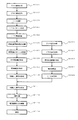
図1及び図2を用いて、本実施形態にかかる有機EL表示装置の製造方法について説明する。図1は、本実施形態にかかる有機EL表示装置の製造方法の概略を示す基板の断面図であり、図2は、本実施形態にかかる有機EL表示装置の製造方法の詳細を示すフローチャートである。 A method for manufacturing the organic EL display device according to the present embodiment will be described with reference to FIGS. FIG. 1 is a cross-sectional view of a substrate showing an outline of a method for manufacturing an organic EL display device according to the present embodiment, and FIG. 2 is a flowchart showing details of the method for manufacturing the organic EL display device according to the present embodiment. .
本実施形態にかかる有機EL表示装置は、画素となる有機EL素子を複数配置した有機EL表示パネルを備えている。有機EL表示パネルは通常、有機EL素子が形成された素子基板と有機EL素子を封止するため、素子基板と対向配置された対向基板とを備えている。 The organic EL display device according to this embodiment includes an organic EL display panel in which a plurality of organic EL elements serving as pixels are arranged. In general, an organic EL display panel includes an element substrate on which an organic EL element is formed and a counter substrate disposed to face the element substrate in order to seal the organic EL element.
図1を用いて、本実施形態にかかる有機EL表示装置の製造方法について説明する。図1は、素子基板である基板10の一部の断面を模式的に示している。
A method for manufacturing the organic EL display device according to the present embodiment will be described with reference to FIG. FIG. 1 schematically shows a partial cross section of a
まず、図1(a)に示すように、基板10を形成する。基板10は、例えば、フロート法により形成された無アルカリガラスである。基板10は上面及び下面にはうねり状の凹凸を有している。しかし、基板10の上面及び下面には、研磨傷などの微小な凹部を有していない。例えば、基板10の厚さは0.7mmである。それに対して、うねりの典型的な形状は、10mmの間隔において、そのうねりの高さが10μm程度の凹凸である。本実施形態では、表面にうねりを有する基板10を機械的に研磨せずに、有機EL素子を形成する。
First, as shown in FIG. 1A, a
次いで、図1(b)に示すように、基板10上にITO101を形成する。ITO101は、陽極となる透明電極であり、例えば、スパッタ等により成膜する。このとき、ITOの表面に微小な突起101aが生ずることがある。この突起101aは、例えば、成膜中のごみや、異常成長によるものである。
Next, as shown in FIG. 1B,
次いで、図1(c)に示すように、ITO101の表面を研磨する。ITO101の表面を研磨することで、突起101aを除去し、ITO101の表面を平坦化する。
Next, as shown in FIG. 1C, the surface of the
次いで、図1(d)に示すように、ITO101上に有機EL層102及び陰極103を形成する。有機EL層102及び陰極103は、例えば、塗布や蒸着等により形成される。基板10に微小な凹凸がないため、ITO101、有機EL層102及び陰極103のそれぞれの厚み方向の形成量が、基板10上において、ほぼ均一となるため、電圧の集中がおきず、ITO101と陰極103の短絡を防止することができる。その後、対向基板を貼り合わせ、封止、切断等を行い、有機EL表示パネルを形成する。
Next, as shown in FIG. 1D, the
次に、図2を用いて、本実施形態にかかる有機EL表示装置の製造方法について詳細に説明する。まず、素子基板に用いるガラス基板をフロート法により形成する(ステップS101)。 Next, the manufacturing method of the organic EL display device according to the present embodiment will be described in detail with reference to FIG. First, a glass substrate used for an element substrate is formed by a float method (step S101).
フロート法では、ガラス原料を溶解窯において溶融ガラスとし、溶融ガラスをフロートバス(溶融金属浴)へ流入し、リボン状のガラスであるガラスリボンを形成する。なお、フロート法によるガラスの製造については、山根 正之他編、「ガラス光学ハンドブック」、第1版、朝倉書店、1999年7月6日、p.359−362、に示されている。 In the float process, a glass raw material is made into molten glass in a melting kiln, and the molten glass flows into a float bath (molten metal bath) to form a glass ribbon which is a ribbon-like glass. For the production of glass by the float process, see Masayuki Yamane et al., “Glass Optical Handbook”, 1st edition, Asakura Shoten, July 6, 1999, p. 359-362.
フロート法で形成したガラスリボンは、ロール等により徐冷窯に搬送され、徐冷窯において徐冷する。ガラスリボンに急激な温度変化が加わると、ひずみが発生するため、一気に冷めないよう、温度調節しながら徐々に冷やす。その後、所望のサイズに切断し、ガラス基板となる。 The glass ribbon formed by the float process is conveyed to a slow cooling kiln by a roll or the like and slowly cooled in the slow cooling kiln. When a sudden temperature change is applied to the glass ribbon, distortion occurs and the glass ribbon is gradually cooled while adjusting the temperature so that it does not cool at once. Then, it cut | disconnects to a desired size and becomes a glass substrate.
また、フロート法により形成されたガラス基板には、溶融金属浴によるSnの表面拡散層が生じるため、塩酸等で洗浄し、Snを除去する(S102)。素子基板となるガラス基板の厚さは、例えば、0.7〜1.1mmである。このように形成されるガラス基板には、例えば、無アルカリガラス(例えば、旭硝子社製AN100)あるいはアルカリガラス(旭硝子社製AS)等があり、本実施形態では、無アルカリガラスを用いる。無アルカリガラスは、アルカリ成分の溶出が少ないため、有機EL素子に与える影響が少ない。このガラス基板の表面は、図1(a)で示したように、うねりを有している。 Further, since a surface diffusion layer of Sn by a molten metal bath is formed on the glass substrate formed by the float process, it is washed with hydrochloric acid or the like to remove Sn (S102). The thickness of the glass substrate used as an element substrate is 0.7-1.1 mm, for example. Examples of the glass substrate thus formed include alkali-free glass (for example, AN100 manufactured by Asahi Glass Co., Ltd.) and alkali glass (ASA manufactured by Asahi Glass Co., Ltd.). In this embodiment, alkali-free glass is used. Alkali-free glass has little influence on the organic EL element because it has little elution of alkali components. The surface of the glass substrate has undulations as shown in FIG.
このガラス基板の溶融金属接触面上に陽極電極材料であるITOを成膜する(ステップS103)。ITOはスパッタや蒸着によって、ガラス基板全面に均一性よく成膜することができる。ここではDCスパッタ法により膜厚150nmで成膜する。フォトリソグラフィー及びエッチングによりITOパターンを形成する(ステップS104)。このITOパターンが陽極となる。レジストとしてはフェノールノボラック樹脂を使用し、露光現像を行う。エッチングはウェットエッチングあるいはドライエッチングのいずれでもよいが、ここでは塩酸及び硝酸の混合水溶液を使用してITOをパターニングした。レジスト剥離材としてはモノエタノールアミンを使用した。ITOの表面には、図1(b)で示したように、突起を生じているため、ITOの表面を研磨することにより、突起等を除去し平坦化する(S105)。 ITO, which is an anode electrode material, is formed on the molten metal contact surface of the glass substrate (step S103). ITO can be formed on the entire surface of the glass substrate with good uniformity by sputtering or vapor deposition. Here, the film is formed with a film thickness of 150 nm by a DC sputtering method. An ITO pattern is formed by photolithography and etching (step S104). This ITO pattern becomes the anode. A phenol novolac resin is used as the resist, and exposure development is performed. Etching may be either wet etching or dry etching. Here, ITO was patterned using a mixed aqueous solution of hydrochloric acid and nitric acid. Monoethanolamine was used as the resist stripping material. As shown in FIG. 1B, protrusions are formed on the surface of the ITO, so that the protrusions and the like are removed and flattened by polishing the surface of the ITO (S105).
ITOパターンの上から補助配線材料を成膜する(ステップS106)。補助配線材料はAlあるいはAl合金などの低抵抗性の金属材料を用い、スパッタ、蒸着によって成膜することができる。さらに下地との密着性を向上させるため、あるいは腐食を防止するために、Al膜の下層又は上層にTiNやCr等のバリア層を形成して補助配線を積層構造としても良い。このバリア層も蒸着あるいはスパッタにより形成できる。ここではDCスパッタ法により総厚が450nmのCr/Al/Crの積層膜やMoNb/Al/MoNbの積層膜を補助配線材料として成膜する。 An auxiliary wiring material is deposited on the ITO pattern (step S106). The auxiliary wiring material can be formed by sputtering or vapor deposition using a low-resistance metal material such as Al or Al alloy. Further, in order to improve adhesion to the base or prevent corrosion, a barrier layer such as TiN or Cr may be formed on the lower layer or upper layer of the Al film to form the auxiliary wiring in a laminated structure. This barrier layer can also be formed by vapor deposition or sputtering. Here, a Cr / Al / Cr laminated film or a MoNb / Al / MoNb laminated film having a total thickness of 450 nm is formed as an auxiliary wiring material by DC sputtering.
この補助配線材料をフォトリソグラフィー及びエッチングによりパターニングして、補助配線パターンを形成する(ステップS107)。エッチングには燐酸、酢酸、硝酸等の混合水溶液よりなるエッチング液を使用することができる。なお、陽極材料と補助配線材料とを順に成膜し、その後に補助配線材料と陽極材料を順番にパターニングすることも可能である。この補助配線パターンにより、陽極又は陰極に信号が供給される。 The auxiliary wiring material is patterned by photolithography and etching to form an auxiliary wiring pattern (step S107). For the etching, an etching solution made of a mixed aqueous solution of phosphoric acid, acetic acid, nitric acid or the like can be used. It is also possible to form the anode material and the auxiliary wiring material in order, and then pattern the auxiliary wiring material and the anode material in order. A signal is supplied to the anode or the cathode by the auxiliary wiring pattern.
次に開口絶縁膜を形成する(ステップS108)。絶縁膜としては感光性のポリイミドをスピンコーティングして、フォトリソグラフィー工程でパターニングした後、キュアし画素に画素開口部を有する開口絶縁膜を形成する。同時に陰極と補助配線とのコンタクトホールを形成する。例えば、画素開口部は300μm×300μm程度、陰極と補助配線とのコンタクトホールを200μm×200μm程度で形成する。なお、画素開口部よりも広い間隔でガラス基板のうねりが存在しているので、画素開口部においては、ガラス基板の表面形状はほぼ平坦である。 Next, an opening insulating film is formed (step S108). As the insulating film, photosensitive polyimide is spin-coated, patterned after a photolithography process, and then cured to form an opening insulating film having a pixel opening in a pixel. At the same time, a contact hole between the cathode and the auxiliary wiring is formed. For example, the pixel opening is formed with a size of about 300 μm × 300 μm, and the contact hole between the cathode and the auxiliary wiring is formed with a size of about 200 μm × 200 μm. Since the glass substrate has waviness at a wider interval than the pixel opening, the surface shape of the glass substrate is almost flat in the pixel opening.
次に陰極隔壁を形成する(ステップS109)。陰極隔壁には、例えば、ノボラック樹脂を用いる。ノボラック樹脂をスピンコートして、フォトリソグラフィー工程でパターニングした後、光反応させて陰極隔壁を形成する。陰極隔壁が逆テーパ構造を有するようネガタイプの感光性樹脂を用いることが好ましい。ネガタイプの感光性樹脂を用いると、上から光を照射した場合、深い場所ほど光反応が不十分となる。その結果、上から見た場合、硬化部分の断面積が上の方より下の方が狭い構造を有する。これが逆テーパ構造を有するという意味である。このような構造にすると、その後、陰極の蒸着時に蒸着源から見て陰になる部分は蒸着が及ばないため、陰極同士を分離することが可能になる。さらに、開口部のITO層の表面改質を行うために、酸素プラズマ又は紫外線を照射してもよい。 Next, a cathode barrier is formed (step S109). For the cathode partition, for example, novolac resin is used. A novolak resin is spin-coated, patterned by a photolithography process, and then photoreacted to form cathode barrier ribs. It is preferable to use a negative type photosensitive resin so that the cathode partition has an inversely tapered structure. When a negative photosensitive resin is used, when light is irradiated from above, the photoreaction becomes insufficient at deeper locations. As a result, when viewed from above, the cross-sectional area of the cured portion has a structure that is narrower on the lower side than on the upper side. This means that it has an inverted taper structure. With such a structure, the cathodes can be separated from each other because the portions that are shaded when viewed from the vapor deposition source during vapor deposition of the cathodes do not reach the vapor deposition. Further, oxygen plasma or ultraviolet light may be irradiated in order to modify the surface of the ITO layer in the opening.
次に画素開口部の上に有機EL素子を形成する(ステップS110)。例えば、蒸着装置を用い、有機EL層と陰極を蒸着する。有機EL層は界面層、正孔輸送層、発光層、電子注入層等を構成要素とすることが多い。ただし、これとは異なる層構成を有する場合もある。有機EL層の厚さは通常100〜300nm程度である。界面層として銅フタロシアニン(CuPc)を厚さ10nm、正孔輸送層としてN,N'−ジ(ナフタレン−1−イル)−N,N'−ジフェニル−ベンジジン(α―NPD)を厚さ60nm、発光層としてAlqを厚さ50nm、電子注入層としてLiFを厚さ0.5nm蒸着する。上述の構成で正孔輸送層をα―NPDの代わりにトリフェニルジアミン(TPD)等のトリフェニルアミン系の物質を使用することもできる。 Next, an organic EL element is formed on the pixel opening (step S110). For example, an organic EL layer and a cathode are deposited using a deposition apparatus. The organic EL layer often includes an interface layer, a hole transport layer, a light emitting layer, an electron injection layer, and the like as constituent elements. However, it may have a different layer structure. The thickness of the organic EL layer is usually about 100 to 300 nm. Copper phthalocyanine (CuPc) is 10 nm thick as the interface layer, and N, N′-di (naphthalen-1-yl) -N, N′-diphenyl-benzidine (α-NPD) is 60 nm thick as the hole transport layer, Alq is deposited to a thickness of 50 nm as a light emitting layer, and LiF is deposited to a thickness of 0.5 nm as an electron injection layer. In the above structure, a triphenylamine-based material such as triphenyldiamine (TPD) can be used for the hole transport layer instead of α-NPD.
陰極にはAlを使用することが多いが、Li等のアルカリ金属、Ag、Ca、Mg、Y、Inやそれらを含む合金を用いることもできる。陰極の厚さは通常50〜300nm程度であり、ここでは厚さ200nmのAlとする。陰極はこの他、スパッタリング、イオンプレーティングなどの物理的気相成長法(PVD)で形成することができる。これにより、有機EL素子を形成する。 Al is often used for the cathode, but alkali metals such as Li, Ag, Ca, Mg, Y, In, and alloys containing them can also be used. The thickness of the cathode is usually about 50 to 300 nm, and here it is Al having a thickness of 200 nm. In addition, the cathode can be formed by physical vapor deposition (PVD) such as sputtering or ion plating. Thereby, an organic EL element is formed.
これらの工程により有機EL素子が複数形成された大型素子基板が製造される。通常1枚の基板には複数の有機EL素子を有する有機EL表示パネルが複数形成される。そして、各有機EL表示パネルを切断分離することにより、1枚のマザーガラスから複数の有機EL表示パネルが得られる。この工程については後述する。上述の有機EL素子基板の製造工程は典型的な有機EL表示装置に用いられる素子基板の製造工程の一例であり、上述の製造工程に限られるものではない。 Through these steps, a large element substrate on which a plurality of organic EL elements are formed is manufactured. Usually, a plurality of organic EL display panels having a plurality of organic EL elements are formed on one substrate. Then, by cutting and separating each organic EL display panel, a plurality of organic EL display panels can be obtained from one mother glass. This process will be described later. The manufacturing process of the organic EL element substrate described above is an example of a manufacturing process of an element substrate used in a typical organic EL display device, and is not limited to the manufacturing process described above.
次に有機EL素子を封止するための対向基板の製造工程について説明する。有機EL素子は空気中の水分により劣化するので、対向基板を用いて封止する。対向基板として厚さ0.7〜1.1mmのガラス基板をフロート法により形成し(ステップS201)、塩酸等により洗浄する(ステップS202)。ガラス基板には、素子基板と同様のものを用いてもよいし、研磨した基板を用いてもよい。そして、この対向基板を加工して、水分を捕獲する捕水材を配置するための捕水材収納部を設ける(ステップS203)。捕水材収納部は例えば、エッチングやサンドブラストにより、対向基板の一部を掘り込むことによって形成される。この捕水材収納部に捕水材を配置する(ステップS204)。捕水材には酸化カルシウム粉末や捕水テープなどが用いられる。 Next, a manufacturing process of the counter substrate for sealing the organic EL element will be described. Since the organic EL element deteriorates due to moisture in the air, it is sealed using a counter substrate. A glass substrate having a thickness of 0.7 to 1.1 mm is formed as a counter substrate by a float method (step S201) and washed with hydrochloric acid or the like (step S202). As the glass substrate, the same substrate as the element substrate may be used, or a polished substrate may be used. Then, the counter substrate is processed to provide a water catching material storage unit for placing a water catching material that captures moisture (step S203). The water catching material storage part is formed, for example, by digging a part of the counter substrate by etching or sandblasting. A water catching material is disposed in the water catching material storage unit (step S204). As the water catching material, calcium oxide powder, water catching tape or the like is used.
そして、対向基板の捕水材収納部を設けた面に、ディスペンサを用いてシール材を塗布する(ステップS205)。シール材を、有機EL表示領域を囲むようにし、有機EL素子を封止するように設ける。さらに切断時に表示パネルから切断される切断端材が飛散するのを防止する飛散防止用シールを各有機EL表示領域間に設ける。封止用シールとしては感光性エポキシ樹脂が好ましい。例えば、光カチオン重合型エポキシ樹脂を用いることができ、素子基板と対向基板を貼り合わせるための接着材として機能する。飛散防止用シールにも同じ材料を使用することができる。これにより、製造工程を簡略化できる。上記の製造工程により封止基板(対向基板)を製造する。なお、上述の製造工程は典型的な一例であり、これに限られるものではない。 And a sealing material is apply | coated to the surface which provided the water catching material accommodating part of the opposing board | substrate using dispenser (step S205). A sealing material is provided so as to surround the organic EL display region and seal the organic EL element. Further, a scattering prevention seal is provided between the organic EL display regions to prevent the cut end material cut from the display panel from being scattered during cutting. As the sealing seal, a photosensitive epoxy resin is preferable. For example, a cationic photopolymerization type epoxy resin can be used and functions as an adhesive for bonding the element substrate and the counter substrate. The same material can be used for the anti-scattering seal. Thereby, a manufacturing process can be simplified. A sealing substrate (counter substrate) is manufactured by the above manufacturing process. The above manufacturing process is a typical example, and the present invention is not limited to this.
次に素子基板と対向基板を貼り合わせて、有機EL素子を封止する(ステップS111)。これ以降の工程について図3及び図4を用いて説明する。図3は基板の構成を示す平面図、図4は封止後の基板の構成を示す断面図である。図3及び図4において、10は素子基板、11は有機EL表示領域、12は補助配線、20は対向基板、21は捕水材収納部、22は捕水材、23は封止用シール、25は飛散防止用シールである。
Next, the element substrate and the counter substrate are bonded together to seal the organic EL element (step S111). The subsequent steps will be described with reference to FIGS. FIG. 3 is a plan view showing the configuration of the substrate, and FIG. 4 is a cross-sectional view showing the configuration of the substrate after sealing. 3 and 4, 10 is an element substrate, 11 is an organic EL display region, 12 is an auxiliary wiring, 20 is a counter substrate, 21 is a water catching material storage unit, 22 is a water catching material, 23 is a sealing seal,
素子基板10には上述のステップS101〜S110により形成し有機EL素子を複数含む有機EL表示領域11と各素子に信号を供給する補助配線12を備えている。図3に示すように素子基板10には6個の有機EL表示領域11を設けており、基板を切断分離することにより有機EL表示パネル30を形成する。素子基板10より若干小さい対向基板20には各有機EL表示領域11に対して捕水材収納部21を形成し、捕水材22を配置している。対向基板20にはそれぞれの有機EL表示領域11を囲む封止用シール23を設ける。さらに、それぞれの有機EL表示領域11に対応する封止用シール23の間には飛散防止用シール25を設ける。
The
素子基板10と対向基板20とが対向するよう位置合わせして、両基板を加圧し、各シール材にUV光を照射する。これにより、図4に示すように両基板が接着された構成となる。素子基板10に設けられたそれぞれの有機EL表示領域11は図3に示すように封止用シール23で全周を囲まれる。両基板と封止用シール23で囲まれた空間に捕水材22を配置し、封止された空間に残留または侵入してくる水分等による有機EL素子の劣化を防止する。素子基板10と対向基板20からなる1対の基板で有機EL素子を封止する。補助配線12は外部の駆動回路と接続するため、封止用シール23の一部は補助配線12をまたがって接着されるようにする。
Positioning is performed so that the
また、素子基板10と対向基板20の外面、すなわち、素子基板10の有機EL素子が設けられた面の反対面及び対向基板20の捕水材22を設けた面の反対面を、研磨等することにより、基板を薄型化してもよい。例えば、各基板を薄型化し0.5mmの厚さとすると、総厚1.0mmの有機EL表示パネル30が得られる。
Further, the outer surfaces of the
封止された基板を切断してそれぞれの有機EL表示パネル30を分離する(ステップS112)。例えば、素子基板10と対向基板20では切断位置が異なる。対向基板20は、封止用シール23周辺を囲むように切断する。素子基板10は、封止用シール23周辺及び補助配線12の端部を囲むように切断する。したがって、素子基板10は封止用シール23の外側に設けた補助配線12の分だけ対向基板20よりも有機EL表示領域11の外側で切断する。これにより、それぞれの有機EL表示パネル30に分割できる。
The sealed substrate is cut to separate each organic EL display panel 30 (step S112). For example, the cutting position is different between the
次に、駆動回路等を実装する(ステップS113)。素子基板10には封止用シール23で囲まれた領域から外に補助配線12を延設する。補助配線12の外側の端部には端子部が形成されており、この端子部に異方性導電フィルム(ACF)を貼付け、駆動回路が設けられたTCP(Tape Carrier Package)を接続する。具体的には端子部にACFを仮圧着する。ACFは日立化成製アニソルム7106Uを用いている。仮圧着温度は80℃で、圧着圧力は1.0MPa、圧着時間は5秒である。ついで駆動回路が内蔵されたTCPを端子部に本圧着する。本圧着温度は170度で、圧着圧力は2.0MPa、圧着時間は20秒である。これにより駆動回路を実装する。この有機EL表示パネル30を筐体に取り付け、有機EL表示装置が完成する(ステップS114)。
Next, a drive circuit and the like are mounted (step S113). On the
このように、うねりを有し研磨傷等の微小な凹凸のないガラス基板を用いることにより、有機EL素子の特性を向上することができる。特に、ガラス基板に研磨傷などが無いことから、研磨したガラス基板に比べて、陽極と陰極の短絡を防止することができる。また、ガラス基板のうねりの凹凸の間隔が、表示画素よりも大きいことから、表示画素内においてガラス基板は平坦であり、うねりによる素子の特性への影響はない。 Thus, the characteristics of the organic EL element can be improved by using a glass substrate that has undulations and does not have minute irregularities such as polishing scratches. In particular, since there are no polishing scratches on the glass substrate, a short circuit between the anode and the cathode can be prevented as compared with a polished glass substrate. Further, since the interval between the undulations of the glass substrate is larger than that of the display pixel, the glass substrate is flat in the display pixel, and the undulation does not affect the characteristics of the element.
なお、上述の説明では、基板に無アルカリガラスを用いたが、これに限らず、低アルカリガラス、ソーダ石灰ガラス、石英ガラス等でもよい。また、上述の説明では、フロート法により形成したが、これに限らず、ロールアウト法等でもよい。 In the above description, alkali-free glass is used for the substrate. However, the present invention is not limited to this, and low alkali glass, soda-lime glass, quartz glass, or the like may be used. In the above description, the float method is used. However, the present invention is not limited to this, and a roll-out method or the like may be used.
10 基板
101 ITO
102 有機EL層
103 陰極
11 有機EL表示領域
12 補助配線
20 対向基板、
21 捕水材収納部
22 捕水材
23 封止用シール
25 飛散防止用シール
30 表示パネル
10
102 organic EL layer 103
21 Water catching
Claims (9)
前記ガラス基板のうねり状凹凸面上に形成された第1の電極と、
前記第1の電極の上に形成された有機発光層と、
前記第1の電極との間において前記有機発光層を挟むように形成された第2の電極と、
が備えられた有機EL表示装置。 A glass substrate having a wavy uneven surface;
A first electrode formed on the wavy uneven surface of the glass substrate;
An organic light emitting layer formed on the first electrode;
A second electrode formed so as to sandwich the organic light emitting layer between the first electrode,
An organic EL display device comprising:
前記第1の電極が形成されたガラス基板上に、有機発光層を形成するステップと、
前記有機発光層が形成されたガラス基板上に、前記第1の電極との間において前記有機発光層を挟むように第2の電極を形成するステップと、
を備える有機EL表示装置の製造方法。 Forming a first electrode on the wavy uneven surface of the glass substrate provided with the wavy uneven surface;
Forming an organic light emitting layer on the glass substrate on which the first electrode is formed;
Forming a second electrode on the glass substrate on which the organic light emitting layer is formed so as to sandwich the organic light emitting layer with the first electrode;
A method for manufacturing an organic EL display device comprising:
9. The organic material according to claim 5, 6, 7 or 8, wherein a glass substrate formed by a float method is used as the glass substrate, and the first electrode is formed on a molten metal contact surface or a molten metal non-contact surface. Manufacturing method of EL display device.
Priority Applications (1)
| Application Number | Priority Date | Filing Date | Title |
|---|---|---|---|
| JP2003431011A JP2005190838A (en) | 2003-12-25 | 2003-12-25 | Organic electroluminescence display device and method for manufacturing the same |
Applications Claiming Priority (1)
| Application Number | Priority Date | Filing Date | Title |
|---|---|---|---|
| JP2003431011A JP2005190838A (en) | 2003-12-25 | 2003-12-25 | Organic electroluminescence display device and method for manufacturing the same |
Publications (1)
| Publication Number | Publication Date |
|---|---|
| JP2005190838A true JP2005190838A (en) | 2005-07-14 |
Family
ID=34789212
Family Applications (1)
| Application Number | Title | Priority Date | Filing Date |
|---|---|---|---|
| JP2003431011A Pending JP2005190838A (en) | 2003-12-25 | 2003-12-25 | Organic electroluminescence display device and method for manufacturing the same |
Country Status (1)
| Country | Link |
|---|---|
| JP (1) | JP2005190838A (en) |
Cited By (4)
| Publication number | Priority date | Publication date | Assignee | Title |
|---|---|---|---|---|
| WO2009017035A1 (en) * | 2007-07-27 | 2009-02-05 | Asahi Glass Co., Ltd. | Translucent substrate, method for manufacturing the translucent substrate, organic led element and method for manufacturing the organic led element |
| WO2009060916A1 (en) * | 2007-11-09 | 2009-05-14 | Asahi Glass Co., Ltd. | Light transmitting substrate, method for manufacturing light transmitting substrate, organic led element and method for manufacturing organic led element |
| WO2010084923A1 (en) | 2009-01-26 | 2010-07-29 | 旭硝子株式会社 | Substrate for electronic device and electronic device using same |
| WO2014038559A1 (en) * | 2012-09-04 | 2014-03-13 | 三菱化学株式会社 | Organic electroluminescent device and manufacturing method thereof |
-
2003
- 2003-12-25 JP JP2003431011A patent/JP2005190838A/en active Pending
Cited By (16)
| Publication number | Priority date | Publication date | Assignee | Title |
|---|---|---|---|---|
| US8018140B2 (en) | 2007-07-27 | 2011-09-13 | Asahi Glass Company, Limited | Translucent substrate, process for producing the same, organic LED element and process for producing the same |
| US8427045B2 (en) | 2007-07-27 | 2013-04-23 | Asahi Glass Company, Limited | Translucent substrate, process for producing the same, organic LED element and process for producing the same |
| JP5195755B2 (en) * | 2007-07-27 | 2013-05-15 | 旭硝子株式会社 | Translucent substrate, manufacturing method thereof, organic LED element and manufacturing method thereof |
| WO2009017035A1 (en) * | 2007-07-27 | 2009-02-05 | Asahi Glass Co., Ltd. | Translucent substrate, method for manufacturing the translucent substrate, organic led element and method for manufacturing the organic led element |
| WO2009060916A1 (en) * | 2007-11-09 | 2009-05-14 | Asahi Glass Co., Ltd. | Light transmitting substrate, method for manufacturing light transmitting substrate, organic led element and method for manufacturing organic led element |
| JPWO2009060916A1 (en) * | 2007-11-09 | 2011-03-24 | 旭硝子株式会社 | Translucent substrate, manufacturing method thereof, organic LED element and manufacturing method thereof |
| US8431943B2 (en) | 2007-11-09 | 2013-04-30 | Asahi Glass Company, Limited | Light transmitting substrate, method for manufacturing light transmitting substrate, organic LED element and method for manufacturing organic LED element |
| JP5824807B2 (en) * | 2009-01-26 | 2015-12-02 | 旭硝子株式会社 | Electronic device substrate and electronic device using the same |
| WO2010084923A1 (en) | 2009-01-26 | 2010-07-29 | 旭硝子株式会社 | Substrate for electronic device and electronic device using same |
| US8729593B2 (en) | 2009-01-26 | 2014-05-20 | Asahi Glass Company, Limited | Substrate with wavy surface to control specular visibility for electronic device and electronic device using same |
| WO2014038559A1 (en) * | 2012-09-04 | 2014-03-13 | 三菱化学株式会社 | Organic electroluminescent device and manufacturing method thereof |
| US20150179963A1 (en) * | 2012-09-04 | 2015-06-25 | Mitsubishi Chemical Corporation | Organic electroluminescent device and method for producing the same |
| EP2894942A4 (en) * | 2012-09-04 | 2015-10-07 | Mitsubishi Chem Corp | Organic electroluminescent device and manufacturing method thereof |
| CN104604332A (en) * | 2012-09-04 | 2015-05-06 | 三菱化学株式会社 | Organic electroluminescent device and manufacturing method thereof |
| JPWO2014038559A1 (en) * | 2012-09-04 | 2016-08-12 | 三菱化学株式会社 | Organic electroluminescent device and manufacturing method thereof |
| CN104604332B (en) * | 2012-09-04 | 2017-03-29 | 三菱化学株式会社 | Organic electroluminescent device and its manufacture method |
Similar Documents
| Publication | Publication Date | Title |
|---|---|---|
| KR20000023402A (en) | Optical device and its manufacture | |
| KR20130130352A (en) | Method for manufacturing organic light emitting display panel | |
| KR20190044015A (en) | Display device and method of manufacturing of the same | |
| TW201735418A (en) | Deposition mask, method for producing deposition mask and method for producing organic semiconductor device | |
| WO2015000186A1 (en) | Oled panel and packaging method therefor | |
| JP2003208975A (en) | Manufacturing method of organic el device | |
| CN106848103B (en) | O L ED substrate, manufacturing method thereof and display device | |
| US7098591B1 (en) | Transparent electrode material for quality enhancement of OLED devices | |
| JP2009117214A (en) | Organic el display panel | |
| JP2008208426A (en) | Mask for film deposition and method for producing mask for film deposition | |
| JP2004296297A (en) | Manufacturing method of wiring board for organic el display device and organic el display device | |
| JP2005285573A (en) | Display device and its manufacturing method | |
| JP2005190838A (en) | Organic electroluminescence display device and method for manufacturing the same | |
| CN112080721A (en) | Mask plate and preparation method thereof, display substrate and display device | |
| JP2005108678A (en) | Organic el light emitting device and its manufacturing method | |
| KR20030084746A (en) | Manufacturing method of electroluminescence display device | |
| CN111525016A (en) | Display panel and manufacturing method thereof | |
| JP2006002243A (en) | Mask, method for producing mask, film deposition method, electronic device and electronic equipment | |
| JP2005078932A (en) | Organic el light emitting device and its manufacturing method | |
| JP2004273438A (en) | Etching mask | |
| JP2008010275A (en) | Image display device | |
| JP2007005047A (en) | Organic el display device and manufacturing method of the same | |
| JP4581664B2 (en) | Semiconductor substrate manufacturing method, semiconductor element manufacturing method, and electro-optical device manufacturing method | |
| JP4486840B2 (en) | Display device and manufacturing method thereof | |
| KR100671975B1 (en) | Shadow mask and the method of its fabrication for OLED |
Legal Events
| Date | Code | Title | Description |
|---|---|---|---|
| A621 | Written request for application examination |
Free format text: JAPANESE INTERMEDIATE CODE: A621 Effective date: 20060809 |
|
| A711 | Notification of change in applicant |
Free format text: JAPANESE INTERMEDIATE CODE: A711 Effective date: 20080218 |
|
| A521 | Request for written amendment filed |
Free format text: JAPANESE INTERMEDIATE CODE: A821 Effective date: 20080218 |
|
| A977 | Report on retrieval |
Free format text: JAPANESE INTERMEDIATE CODE: A971007 Effective date: 20090803 |
|
| A131 | Notification of reasons for refusal |
Free format text: JAPANESE INTERMEDIATE CODE: A131 Effective date: 20090811 |
|
| A02 | Decision of refusal |
Free format text: JAPANESE INTERMEDIATE CODE: A02 Effective date: 20100302 |