JP2005183943A - Semiconductor device - Google Patents
Semiconductor device Download PDFInfo
- Publication number
- JP2005183943A JP2005183943A JP2004339608A JP2004339608A JP2005183943A JP 2005183943 A JP2005183943 A JP 2005183943A JP 2004339608 A JP2004339608 A JP 2004339608A JP 2004339608 A JP2004339608 A JP 2004339608A JP 2005183943 A JP2005183943 A JP 2005183943A
- Authority
- JP
- Japan
- Prior art keywords
- silicon carbide
- carbide layer
- semiconductor element
- region
- electrode
- Prior art date
- Legal status (The legal status is an assumption and is not a legal conclusion. Google has not performed a legal analysis and makes no representation as to the accuracy of the status listed.)
- Pending
Links
- 239000004065 semiconductor Substances 0.000 title claims abstract description 119
- 229910010271 silicon carbide Inorganic materials 0.000 claims abstract description 183
- HBMJWWWQQXIZIP-UHFFFAOYSA-N silicon carbide Chemical compound [Si+]#[C-] HBMJWWWQQXIZIP-UHFFFAOYSA-N 0.000 claims abstract description 163
- 239000000758 substrate Substances 0.000 claims abstract description 80
- 229910021478 group 5 element Inorganic materials 0.000 claims abstract description 25
- IJGRMHOSHXDMSA-UHFFFAOYSA-N Atomic nitrogen Chemical compound N#N IJGRMHOSHXDMSA-UHFFFAOYSA-N 0.000 claims description 50
- 229910052757 nitrogen Inorganic materials 0.000 claims description 26
- 238000010438 heat treatment Methods 0.000 claims description 24
- 239000013078 crystal Substances 0.000 claims description 21
- MWUXSHHQAYIFBG-UHFFFAOYSA-N Nitric oxide Chemical group O=[N] MWUXSHHQAYIFBG-UHFFFAOYSA-N 0.000 claims description 17
- 239000012535 impurity Substances 0.000 claims description 17
- 150000001875 compounds Chemical class 0.000 claims description 11
- 230000001590 oxidative effect Effects 0.000 claims description 9
- 238000007669 thermal treatment Methods 0.000 abstract 1
- 239000010410 layer Substances 0.000 description 169
- 108091006146 Channels Proteins 0.000 description 66
- 239000013598 vector Substances 0.000 description 41
- 238000000034 method Methods 0.000 description 18
- PXHVJJICTQNCMI-UHFFFAOYSA-N Nickel Chemical compound [Ni] PXHVJJICTQNCMI-UHFFFAOYSA-N 0.000 description 16
- 239000000969 carrier Substances 0.000 description 11
- XAGFODPZIPBFFR-UHFFFAOYSA-N aluminium Chemical compound [Al] XAGFODPZIPBFFR-UHFFFAOYSA-N 0.000 description 8
- 229910052782 aluminium Inorganic materials 0.000 description 8
- 229910052759 nickel Inorganic materials 0.000 description 8
- 238000003860 storage Methods 0.000 description 8
- 238000010586 diagram Methods 0.000 description 7
- 230000000694 effects Effects 0.000 description 7
- 239000007789 gas Substances 0.000 description 7
- 238000000137 annealing Methods 0.000 description 5
- 230000008878 coupling Effects 0.000 description 5
- 238000010168 coupling process Methods 0.000 description 5
- 238000005859 coupling reaction Methods 0.000 description 5
- 238000004519 manufacturing process Methods 0.000 description 5
- 229910004298 SiO 2 Inorganic materials 0.000 description 3
- QVGXLLKOCUKJST-UHFFFAOYSA-N atomic oxygen Chemical compound [O] QVGXLLKOCUKJST-UHFFFAOYSA-N 0.000 description 3
- 238000009413 insulation Methods 0.000 description 3
- 239000011229 interlayer Substances 0.000 description 3
- 229910052760 oxygen Inorganic materials 0.000 description 3
- 239000001301 oxygen Substances 0.000 description 3
- ODUCDPQEXGNKDN-UHFFFAOYSA-N Nitrogen oxide(NO) Natural products O=N ODUCDPQEXGNKDN-UHFFFAOYSA-N 0.000 description 2
- OAICVXFJPJFONN-UHFFFAOYSA-N Phosphorus Chemical compound [P] OAICVXFJPJFONN-UHFFFAOYSA-N 0.000 description 2
- XUIMIQQOPSSXEZ-UHFFFAOYSA-N Silicon Chemical compound [Si] XUIMIQQOPSSXEZ-UHFFFAOYSA-N 0.000 description 2
- 239000004020 conductor Substances 0.000 description 2
- 239000007772 electrode material Substances 0.000 description 2
- 230000012447 hatching Effects 0.000 description 2
- 238000002513 implantation Methods 0.000 description 2
- 238000002347 injection Methods 0.000 description 2
- 239000007924 injection Substances 0.000 description 2
- 238000005468 ion implantation Methods 0.000 description 2
- 230000003647 oxidation Effects 0.000 description 2
- 238000007254 oxidation reaction Methods 0.000 description 2
- 229910052698 phosphorus Inorganic materials 0.000 description 2
- 239000011574 phosphorus Substances 0.000 description 2
- 229910052710 silicon Inorganic materials 0.000 description 2
- 239000010703 silicon Substances 0.000 description 2
- QGZKDVFQNNGYKY-UHFFFAOYSA-N Ammonia Chemical compound N QGZKDVFQNNGYKY-UHFFFAOYSA-N 0.000 description 1
- OKTJSMMVPCPJKN-UHFFFAOYSA-N Carbon Chemical compound [C] OKTJSMMVPCPJKN-UHFFFAOYSA-N 0.000 description 1
- 102000004129 N-Type Calcium Channels Human genes 0.000 description 1
- 108090000699 N-Type Calcium Channels Proteins 0.000 description 1
- 238000009825 accumulation Methods 0.000 description 1
- 230000004913 activation Effects 0.000 description 1
- 229910052785 arsenic Inorganic materials 0.000 description 1
- RQNWIZPPADIBDY-UHFFFAOYSA-N arsenic atom Chemical compound [As] RQNWIZPPADIBDY-UHFFFAOYSA-N 0.000 description 1
- 229910052799 carbon Inorganic materials 0.000 description 1
- 230000015556 catabolic process Effects 0.000 description 1
- 230000006837 decompression Effects 0.000 description 1
- 230000007423 decrease Effects 0.000 description 1
- 230000007547 defect Effects 0.000 description 1
- 238000009826 distribution Methods 0.000 description 1
- 230000007613 environmental effect Effects 0.000 description 1
- 238000009499 grossing Methods 0.000 description 1
- 230000005524 hole trap Effects 0.000 description 1
- 239000011261 inert gas Substances 0.000 description 1
- 239000000463 material Substances 0.000 description 1
- 229910003465 moissanite Inorganic materials 0.000 description 1
- 238000005498 polishing Methods 0.000 description 1
- 230000003746 surface roughness Effects 0.000 description 1
- 230000002195 synergetic effect Effects 0.000 description 1
- XLYOFNOQVPJJNP-UHFFFAOYSA-N water Chemical compound O XLYOFNOQVPJJNP-UHFFFAOYSA-N 0.000 description 1
Images


Classifications
-
- H—ELECTRICITY
- H01—ELECTRIC ELEMENTS
- H01L—SEMICONDUCTOR DEVICES NOT COVERED BY CLASS H10
- H01L29/00—Semiconductor devices specially adapted for rectifying, amplifying, oscillating or switching and having potential barriers; Capacitors or resistors having potential barriers, e.g. a PN-junction depletion layer or carrier concentration layer; Details of semiconductor bodies or of electrodes thereof ; Multistep manufacturing processes therefor
- H01L29/66—Types of semiconductor device ; Multistep manufacturing processes therefor
- H01L29/68—Types of semiconductor device ; Multistep manufacturing processes therefor controllable by only the electric current supplied, or only the electric potential applied, to an electrode which does not carry the current to be rectified, amplified or switched
- H01L29/76—Unipolar devices, e.g. field effect transistors
- H01L29/772—Field effect transistors
- H01L29/78—Field effect transistors with field effect produced by an insulated gate
- H01L29/7801—DMOS transistors, i.e. MISFETs with a channel accommodating body or base region adjoining a drain drift region
- H01L29/7802—Vertical DMOS transistors, i.e. VDMOS transistors
-
- H—ELECTRICITY
- H01—ELECTRIC ELEMENTS
- H01L—SEMICONDUCTOR DEVICES NOT COVERED BY CLASS H10
- H01L29/00—Semiconductor devices specially adapted for rectifying, amplifying, oscillating or switching and having potential barriers; Capacitors or resistors having potential barriers, e.g. a PN-junction depletion layer or carrier concentration layer; Details of semiconductor bodies or of electrodes thereof ; Multistep manufacturing processes therefor
- H01L29/40—Electrodes ; Multistep manufacturing processes therefor
- H01L29/41—Electrodes ; Multistep manufacturing processes therefor characterised by their shape, relative sizes or dispositions
- H01L29/417—Electrodes ; Multistep manufacturing processes therefor characterised by their shape, relative sizes or dispositions carrying the current to be rectified, amplified or switched
- H01L29/41725—Source or drain electrodes for field effect devices
- H01L29/41766—Source or drain electrodes for field effect devices with at least part of the source or drain electrode having contact below the semiconductor surface, e.g. the source or drain electrode formed at least partially in a groove or with inclusions of conductor inside the semiconductor
Landscapes
- Engineering & Computer Science (AREA)
- Microelectronics & Electronic Packaging (AREA)
- Power Engineering (AREA)
- Physics & Mathematics (AREA)
- Ceramic Engineering (AREA)
- Condensed Matter Physics & Semiconductors (AREA)
- General Physics & Mathematics (AREA)
- Computer Hardware Design (AREA)
- Insulated Gate Type Field-Effect Transistor (AREA)
Abstract
Description
本発明は高耐圧、炭化珪素を用いた絶縁ゲート型半導体素子に関するものであり、特に、大電流のスイッチング素子を実現するMOSFETに関するものである。 The present invention relates to an insulated gate semiconductor device using high breakdown voltage and silicon carbide, and more particularly to a MOSFET that realizes a large current switching device.
炭化珪素(シリコンカーバイド、SiC)は、珪素(Si)に比べて高硬度でワイドバンドギャップを有する半導体であり、パワー素子や耐環境素子、高温動作素子、高周波素子等へ応用されている。 Silicon carbide (silicon carbide, SiC) is a semiconductor having higher hardness and wider band gap than silicon (Si), and is applied to power elements, environmental resistance elements, high temperature operation elements, high frequency elements and the like.
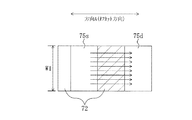
SiCを用いたスイッチング素子の代表的なものとして、例えば以下の特許文献1に開示されるようなMOSFETが知られている。図14(a), (b)は、SiCを用いた一般的な縦型蓄積型MOSFETを示す図である。なお、一般的な縦型のMOSFETにおいて、ユニットセルとは、ソース電極を中心とした電極の配置をいうのに対し、図14(a), (b)では、ゲート電極を中心とした電極の配置を示している。つまり、図14(a), (b)では、2つのユニットセルの結合部を示している。ここで、図14(a)は、MOSFETの電極の一部を上方から見た平面図であり、図14(b)は、図14(a)に示すXI-XI線における断面図である。
As a representative switching element using SiC, for example, a MOSFET as disclosed in
図14(a), (b)に示すように、従来の縦型蓄積型MOSFETでは、n+ 型の4H−SiCからなる半導体基板101と、半導体基板101の上に設けられ、n型の4H−SiCからなるn型炭化珪素層102と、n型炭化珪素層102の上部のうち2つのユニットセルの結合部の両側方に位置する領域に設けられ、例えばアルミニウムが注入されたp型ウェル領域103と、n型炭化珪素層102のうち2つのp型ウェル領域103に挟まれる領域の上から、その2つのp型ウェル領域103の上に亘って延びる、例えばn型の4H−SiCからなるチャネル層104と、p型ウェル領域103の上部に、チャネル層104の外側方と接するように設けられ、例えば窒素が注入されたソース領域105と、チャネル層104の上から、ソース領域105の一部の上に亘って設けられたゲート絶縁膜106と、ゲート絶縁膜106の上に設けられたゲート電極107と、ソース領域105の上から、n型炭化珪素層102のうちソース領域105の外側方に位置する部分の上に亘って設けられたソース電極108と、半導体基板101の下面上に設けられたドレイン電極109とを備えている。
As shown in FIGS. 14A and 14B, in the conventional vertical storage MOSFET, a
ソース電極108は、p型ウェル領域103と電気的に接続されるベース電極としての役割を兼ね備えた構造を有している。
The
MOSFETをONの状態にするためには、ドレイン電極109にプラスの電圧を印加し、ソース電極108を接地し、ゲート電極107にプラスの電圧を印加する。これにより、MOSFETのスイッチング動作が可能となる。
In order to turn on the MOSFET, a positive voltage is applied to the
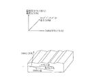
ここで、MOSFETがONの状態になると、キャリアである電子は、図14(a), (b)に示すように、まず、基板面に平行な方向に流れる。その後に、電子は、図14(b)に示すように、基板面に垂直な方向に流れる。なお、図14(a), (b)に示す矢印は、キャリアである電子の進む方向を示しており、電流はこの矢印と逆の向きに流れる。ここで注目すべきなのが、図14(a)に示す電子の進行方向である。ソース電極108やゲート電極107が、基板のオフカット方向Aと垂直な方向にキャリアが移動するように配置されている。なお、「オフカット方向」とは、結晶面から数度傾いたオフカット面がある場合に、オフカット面内の方向であって、結晶面に対する法線ベクトルからオフカット面に対する法線ベクトルに向かう方向をいう。以下に、電極の配置の理由について、図15を参照しながら説明する。図15は、炭化珪素基板の表面および断面の概略を示す斜視図である。
Here, when the MOSFET is turned on, electrons as carriers first flow in a direction parallel to the substrate surface, as shown in FIGS. Thereafter, the electrons flow in a direction perpendicular to the substrate surface, as shown in FIG. Note that the arrows shown in FIGS. 14A and 14B indicate the direction in which electrons as carriers travel, and the current flows in the direction opposite to this arrow. What should be noted here is the traveling direction of electrons shown in FIG. The
図15に示す炭化珪素基板は、(0001)面に対して所定角度だけオフカットされた基板面を有している。図15では、基板面、すなわちオフカット面を水平に示している。一般的に、炭化珪素基板を用いて素子を形成する場合には(0001)面のオフカット基板が用いられる。その理由は、(0001)面に対する所定のオフカット面をエピタキシャル成長によって形成するときには、ポリタイプ制御が容易であるからである。なお、オフカット面としては、例えば、4H−SiC(0001)に対して、<11−20>方向(ここでは112バー0という意味である。)に約8度オフカットされた面を形成する。 The silicon carbide substrate shown in FIG. 15 has a substrate surface that is cut off by a predetermined angle with respect to the (0001) plane. In FIG. 15, the substrate surface, that is, the off-cut surface is shown horizontally. In general, when an element is formed using a silicon carbide substrate, an offcut substrate having a (0001) plane is used. This is because the polytype control is easy when a predetermined off-cut surface with respect to the (0001) plane is formed by epitaxial growth. Note that as the off-cut surface, for example, a surface that is off-cut about 8 degrees in the <11-20> direction (in this case, 112 bar 0) with respect to 4H—SiC (0001) is formed. .
ただし、オフカット面を基板面に有する基板に対して、エピタキシャル成長や不純物活性化のための熱処理などの高温の処理を適用すると、基板面にはオフカット方向に対して垂直な方向にステップバンチングが形成されてしまうことがある。例えば、オフカット方向が<11−20>方向である場合には、ステップバンチングが、<11−20>方向に対して垂直な方向である<1−100>方向に形成される。ステップバンチングは、50〜100nm程度の凹凸になり、これが原因となって電気特性の異方性が生じることがある。従来では、オフカット方向(ステップバンチングを横切る方向)と、オフカット方向に垂直な方向(ステップバンチングと平行な方向)とで、電子移動度は例えば1桁以上異なる。 However, if high temperature processing such as epitaxial growth or heat treatment for impurity activation is applied to a substrate having an offcut surface on the substrate surface, step bunching is applied to the substrate surface in a direction perpendicular to the offcut direction. May be formed. For example, when the offcut direction is the <11-20> direction, step bunching is formed in the <1-100> direction, which is a direction perpendicular to the <11-20> direction. Step bunching has irregularities of about 50 to 100 nm, and this may cause anisotropy of electrical characteristics. Conventionally, the electron mobility differs by, for example, one digit or more in the off-cut direction (direction across the step bunching) and the direction perpendicular to the off-cut direction (direction parallel to the step bunching).
以上の理由から、電流量の大きい半導体装置を製造するためには、オフカット方向に対して垂直な方向に電流を流すように電極の方向を設計する必要があった。チャネル層104において、複数の方向に電流が流れる場合には、それらの方向のうち最も電流量の多い方向をオフカット方向に対して垂直な方向に合わせて設計する必要があった(例えば、特許文献1参照)。
上述したように、従来では、ステップバンチングが形成されることによって、ステップバンチングに平行な方向の電子移動度が大きくなり、ステップバンチングに対して垂直な方向の電子移動度が小さくなるという前提で、素子の配置が決定されていた。また、表面にステップバンチングが形成されていない場合であっても、炭化珪素内部に積層欠陥などの結晶欠陥が内在し、オフカット方向に対して平行な方向の電子移動度が、オフカット方向に対して垂直な方向の電子移動度よりも小さくなることがあった。しかしながら、電流方向の異方性が逆転する場合があり、その場合には、素子の電気特性をより低くしてしまうことがあった。 As described above, conventionally, by forming step bunching, the electron mobility in the direction parallel to the step bunching increases, and the electron mobility in the direction perpendicular to the step bunching decreases. The arrangement of the elements has been determined. Even when step bunching is not formed on the surface, crystal defects such as stacking faults are present inside silicon carbide, and the electron mobility in the direction parallel to the offcut direction is in the offcut direction. On the other hand, the electron mobility in a direction perpendicular to the vertical direction sometimes became smaller. However, the anisotropy in the current direction may be reversed, and in that case, the electrical characteristics of the element may be further lowered.
本発明の目的は、上述の課題を解決する手段を講ずることにより、より電気特性が優れた炭化珪素半導体素子を提供することにある。 An object of the present invention is to provide a silicon carbide semiconductor element having more excellent electrical characteristics by taking means for solving the above-described problems.
本発明の第1の半導体素子は、半導体基板と、上記半導体基板の上に設けられ、結晶面から10度以下の角度だけオフカット方向に傾いた上面を有する炭化珪素層と、上記炭化珪素層の上に設けられたゲート絶縁膜と、上記ゲート絶縁膜の上に設けられたゲート電極と、上記炭化珪素層の上のうち上記ゲート電極の側方に設けられたソース電極と、上記半導体基板の下方に設けられたドレイン電極と、上記炭化珪素層のうち少なくとも上記ソース電極の下に位置する領域に設けられたソース領域とを備え、平面視して、上記ソース領域のうち最も長い辺は、上記オフカット方向に垂直な方向に沿っている。 A first semiconductor element of the present invention includes a semiconductor substrate, a silicon carbide layer provided on the semiconductor substrate and having an upper surface inclined in an offcut direction by an angle of 10 degrees or less from a crystal plane, and the silicon carbide layer A gate insulating film provided on the gate insulating film; a gate electrode provided on the gate insulating film; a source electrode provided on a side of the gate electrode on the silicon carbide layer; and the semiconductor substrate. And a source region provided at least in a region located below the source electrode in the silicon carbide layer, and the longest side of the source region in plan view is , Along the direction perpendicular to the off-cut direction.
このように、オフカット方向に沿った方向に電流が流れるようにソース領域を配置することにより、より電気特性を向上させることができる。また、電流方向の異方性が逆転するおそれもなくなる。これらは、以下の理由による。従来では、高温の熱処理の際に炭化珪素層のオフカット方向に垂直な方向にステップバンチングが形成され、ステップバンチングに平行な方向の電子移動度が大きかった。これに対し、本発明の半導体素子はV族元
素を含む化合物を用いて熱処理を行う工程を経て形成されるので、炭化珪素層の上面にステップバンチングが形成されていても、チャネル層が形成されるゲート絶縁膜と炭化珪素層の界面において、界面準位密度が低減され、オフカット方向に沿った方向の電子移動度が向上する。これにより、オフカット方向に沿った方向の電子移動度が、オフカット方向に垂直な方向の電子移動度よりも高くなりやすい。
As described above, the electric characteristics can be further improved by arranging the source region so that the current flows in the direction along the off-cut direction. Further, there is no possibility that the anisotropy in the current direction is reversed. These are for the following reasons. Conventionally, step bunching is formed in the direction perpendicular to the off-cut direction of the silicon carbide layer during the high-temperature heat treatment, and the electron mobility in the direction parallel to the step bunching has been large. On the other hand, since the semiconductor element of the present invention is formed through a heat treatment process using a compound containing a group V element, a channel layer is formed even if step bunching is formed on the upper surface of the silicon carbide layer. At the interface between the gate insulating film and the silicon carbide layer, the interface state density is reduced, and the electron mobility in the direction along the offcut direction is improved. Thereby, the electron mobility in the direction along the off-cut direction tends to be higher than the electron mobility in the direction perpendicular to the off-cut direction.
上記炭化珪素層のうち上記ソース領域の側方および下方に設けられた第2導電型のウェル領域と、上記ウェル領域と電気的に接続されるベース電極とをさらに備えていてもよい。 The silicon carbide layer may further include a second conductivity type well region provided laterally and below the source region, and a base electrode electrically connected to the well region.
上記オフカット方向に垂直な方向に沿った方向とは、上記オフカット方向に垂直な方向からの傾きが5度以内の方向であることにより、高い電子移動度を得ることができる。 The direction along the direction perpendicular to the offcut direction is a direction whose inclination from the direction perpendicular to the offcut direction is within 5 degrees, so that high electron mobility can be obtained.
上記炭化珪素層のうち上記ゲート絶縁膜の下に位置する領域にチャネル層が設けられていてもよい。 A channel layer may be provided in a region located below the gate insulating film in the silicon carbide layer.
上記チャネル領域には、少なくとも1層の第1炭化珪素層と、第1炭化珪素層よりも第1導電型の不純物濃度が高くかつ第1炭化珪素層の膜厚よりも薄い、少なくとも1層の第2炭化珪素層とを有する積層構造が設けられていてもよい。この場合には、さらに高い電子移動度を得ることができる。 The channel region includes at least one first silicon carbide layer and at least one layer having a first conductivity type impurity concentration higher than that of the first silicon carbide layer and less than the thickness of the first silicon carbide layer. A laminated structure having a second silicon carbide layer may be provided. In this case, higher electron mobility can be obtained.
上記炭化珪素層において、結晶面の面内方向における電子移動度よりも、上記結晶面に対する垂直方向における電子移動度の方が大きい場合に、本発明は有効である。 In the silicon carbide layer, the present invention is effective when the electron mobility in the direction perpendicular to the crystal plane is larger than the electron mobility in the in-plane direction of the crystal plane.
上記炭化珪素層は、4H−SiCであってもよい。 The silicon carbide layer may be 4H—SiC.
上記炭化珪素層の上面は、(0001)面から<11−20>方向に傾いた面であってもよい。 The upper surface of the silicon carbide layer may be a surface inclined in the <11-20> direction from the (0001) plane.
上記炭化珪素層の上面は、(0001)面から<1−100>方向に傾いた面であってもよい。 The upper surface of the silicon carbide layer may be a surface inclined in the <1-100> direction from the (0001) plane.
上記ゲート絶縁膜が、上記炭化珪素層の上部を熱酸化した後に、V族元素を含む化合物
を含む雰囲気で熱処理することにより形成された場合には、上記界面準位密度を低下させることができ、その結果、オフカット方向における電子移動度が高くなる。
When the gate insulating film is formed by thermally oxidizing the upper portion of the silicon carbide layer and then heat-treating in an atmosphere containing a compound containing a group V element, the interface state density can be reduced. As a result, the electron mobility in the off-cut direction is increased.
上記V族元素を含む化合物が、酸化窒素(NxOy(x, y=1, 2, ・・・))であ
る場合には、高い効果を得ることができる。
When the compound containing the Group V element is nitrogen oxide (N x O y (x, y = 1, 2,...)), A high effect can be obtained.
上記炭化珪素層と上記ゲート絶縁膜との界面において、上記チャネル層と上記ゲート絶縁膜との界面において、窒素濃度の最大値が1×1020cm-3以上で1×1022cm-3以下であることが好ましい。この場合には、各バンド端付近のポテンシャル範囲において界面密度を十分低くすることができるため、炭化珪素層の上面部とゲート酸化膜との間にステップバンチングが発生していても発生していなくても良好な界面が形成される。 At the interface between the silicon carbide layer and the gate insulating film, the maximum value of the nitrogen concentration at the interface between the channel layer and the gate insulating film is 1 × 10 20 cm −3 or more and 1 × 10 22 cm −3 or less. It is preferable that In this case, since the interface density can be sufficiently lowered in the potential range near each band edge, even if step bunching occurs between the upper surface portion of the silicon carbide layer and the gate oxide film, it does not occur. However, a good interface is formed.
ここで、上記ゲート絶縁膜が、上記炭化珪素層の上部をV族元素を含む化合物を含む雰
囲気で熱酸化することにより形成された場合であっても、ゲート絶縁膜と炭化珪素層の界面は良好なものが得られ、特に上記の酸化窒素を含む雰囲気で熱酸化して形成されたゲート絶縁膜も本発明に対して有効に働く。
Here, even when the gate insulating film is formed by thermally oxidizing the upper portion of the silicon carbide layer in an atmosphere containing a compound containing a group V element, the interface between the gate insulating film and the silicon carbide layer is A good one can be obtained, and in particular, the gate insulating film formed by thermal oxidation in an atmosphere containing the above-described nitric oxide also works effectively for the present invention.
上記炭化珪素層が第1導電型の不純物を含み、上記炭化珪素層の上のうち上記ゲート電極の側方に設けられたソース電極と、上記半導体基板の下方に設けられたドレイン電極と、上記炭化珪素層のうち少なくとも上記ソース電極の下に位置する領域に設けられ、上記チャネル層に接する第1導電型のソース領域と、上記炭化珪素層のうち上記ソース領域の側方および下方を囲む第2導電型のウェル領域と、上記ウェル領域と電気的に接続されるベース電極とをさらに備える場合には、縦型のMOSFETにおいて、高い電子移動度を得ることができる。 The silicon carbide layer includes a first conductivity type impurity; a source electrode provided on a side of the gate electrode on the silicon carbide layer; a drain electrode provided below the semiconductor substrate; A first conductivity type source region that is provided in at least a region of the silicon carbide layer located below the source electrode and is in contact with the channel layer; and a side of the silicon carbide layer that surrounds the side and the lower side of the source region. When a two-conductivity type well region and a base electrode electrically connected to the well region are further provided, high electron mobility can be obtained in the vertical MOSFET.
上記ソース電極は、上記ベース電極と同一の膜で設けられていてもよい。 The source electrode may be provided with the same film as the base electrode.
上記ゲート電極は、平面視して多角形がくり抜かれた形状で設けられている場合があり、この場合には、上記多角形におけるくり抜かれた部分の辺のうち最も長い辺は、上記オフカット方向に垂直な方向に沿っていることが好ましい。 The gate electrode may be provided in a shape in which a polygon is cut out in a plan view. In this case, the longest side among the sides of the cut out portion in the polygon is the off cut. It is preferable that the direction is perpendicular to the direction.
この場合には、平面視して、上記ソース電極は多角形の形状で配置し、上記ゲート電極は上記ソース電極と離間して、かつ上記ソース電極の側方を囲む形状で配置していてもよい。 In this case, the source electrode may be arranged in a polygonal shape in plan view, and the gate electrode may be arranged so as to be separated from the source electrode and surround the side of the source electrode. Good.
また、上記ゲート電極が、平面視して多角形の形状で設けられている場合もあり、この場合には、上記多角形の辺のうち最も長い辺は、上記オフカット方向に垂直な方向に沿っていることが好ましい。 In addition, the gate electrode may be provided in a polygonal shape in plan view. In this case, the longest side of the polygonal side is in a direction perpendicular to the offcut direction. It is preferable that it is along.
この場合には、平面視して、上記ソース電極は、ストライプ状に並ぶ複数の第1矩形部と、上記複数の第1矩形部の端部を接続する第1接続部とを有する櫛形に配置し、上記ゲート電極は、上記複数の第1矩形部のそれぞれと交互に配置するストライプ状の複数の第2矩形部と、上記第2矩形部の端部を接続する第2接続部とを有する櫛形に配置していてもよい。 In this case, in plan view, the source electrode is arranged in a comb shape having a plurality of first rectangular portions arranged in a stripe shape and a first connection portion connecting ends of the plurality of first rectangular portions. The gate electrode has a plurality of stripe-shaped second rectangular portions that are alternately arranged with each of the plurality of first rectangular portions, and a second connection portion that connects the ends of the second rectangular portions. It may be arranged in a comb shape.
なお、本明細書中において、「多角形」や「櫛形」といった形には、角部が丸まっているものや、辺が曲線であるものを含むものとする。また、ソース領域が例えば楕円形である場合において、「ソース領域のうち最も長い辺は、上記オフカット方向に垂直な方向である」とは、楕円形の長軸がオフカット方向に垂直な方向に伸びていることをいうものとする。 Note that in this specification, shapes such as “polygon” and “comb” include those having rounded corners and those having curved sides. Further, when the source region is, for example, elliptical, “the longest side of the source region is the direction perpendicular to the offcut direction” means that the major axis of the ellipse is perpendicular to the offcut direction. It means that it is growing.
本発明の第2の半導体素子は、半導体基板と、上記半導体基板の上に設けられ、結晶面から10度以下の角度だけオフカット方向に傾いた上面を有する炭化珪素層と、上記炭化珪素層の上に設けられたゲート絶縁膜と、上記ゲート絶縁膜の上に設けられたゲート電極と、上記炭化珪素層の上のうち上記ゲート電極の側方に設けられたソース電極と、上記炭化珪素層の上のうち上記ゲート電極の側方に設けられたドレイン電極と、上記炭化珪素層のうち少なくとも上記ソース電極および上記ドレイン電極の下に位置する領域に互いに離間して設けられたソース・ドレイン領域とを備え、平面視して、上記ソース・ドレイン領域の辺のうち互いに対向する辺は、上記オフカット方向に垂直な方向に沿っている。 A second semiconductor element of the present invention includes a semiconductor substrate, a silicon carbide layer provided on the semiconductor substrate and having an upper surface inclined in an off-cut direction by an angle of 10 degrees or less from a crystal plane, and the silicon carbide layer A gate insulating film provided on the gate insulating film; a gate electrode provided on the gate insulating film; a source electrode provided on a side of the gate electrode on the silicon carbide layer; and the silicon carbide. The drain electrode provided on the side of the gate electrode on the layer, and the source / drain provided apart from each other in a region of the silicon carbide layer located below the source electrode and the drain electrode When viewed from above, the sides of the source / drain regions facing each other are along a direction perpendicular to the off-cut direction.
このように、オフカット方向に沿った方向に電流が流れるようにソース・ドレイン領域を配置することにより、より電気特性を向上させることができる。これらは、以下の理由による。従来では、高温の熱処理の際に炭化珪素層のオフカット方向に垂直な方向にステップバンチングが形成され、ステップバンチングに平行な方向の電子移動度が大きかった。これに対し、本発明の半導体素子はV族元素を含む化合物を用いて熱処理を行う工程を
経て形成されるので、炭化珪素層の上面にステップバンチングが形成されていても、チャネル層が形成されるゲート絶縁膜と炭化珪素層の界面において、界面準位密度が低減され、オフカット方向に沿った方向の電子移動度が向上する。これにより、オフカット方向に沿った方向の電子移動度が、オフカット方向に垂直な方向の電子移動度よりも高くなりやすい。
As described above, the electrical characteristics can be further improved by arranging the source / drain regions so that the current flows in the direction along the off-cut direction. These are for the following reasons. Conventionally, step bunching is formed in the direction perpendicular to the off-cut direction of the silicon carbide layer during the high-temperature heat treatment, and the electron mobility in the direction parallel to the step bunching has been large. On the other hand, since the semiconductor element of the present invention is formed through a heat treatment process using a compound containing a group V element, a channel layer is formed even if step bunching is formed on the upper surface of the silicon carbide layer. At the interface between the gate insulating film and the silicon carbide layer, the interface state density is reduced, and the electron mobility in the direction along the offcut direction is improved. Thereby, the electron mobility in the direction along the off-cut direction tends to be higher than the electron mobility in the direction perpendicular to the off-cut direction.
上記炭化珪素層内に設けられ、第1導電型の不純物を含むベース領域と、上記ベース領域と電気的に接続されるベース電極とをさらに備えていてもよい。 A base region provided in the silicon carbide layer and including a first conductivity type impurity, and a base electrode electrically connected to the base region may be further provided.
上記ゲート電極は多角形の形状で設けられている場合もあり、この場合には、上記多角形の辺のうち最も長い辺は、上記オフカット方向に垂直な方向に沿っていることが好ましい。 The gate electrode may be provided in a polygonal shape, and in this case, the longest side of the polygonal side is preferably along a direction perpendicular to the offcut direction.
上記オフカット方向に垂直な方向に沿った方向とは、上記オフカット方向に垂直な方向からの傾きが5度以内の方向であることにより、高い電子移動度を得ることができる。 The direction along the direction perpendicular to the offcut direction is a direction whose inclination from the direction perpendicular to the offcut direction is within 5 degrees, so that high electron mobility can be obtained.
上記炭化珪素層のうち上記ゲート絶縁膜の下に位置する領域にチャネル層が設けられていてもよい。 A channel layer may be provided in a region located below the gate insulating film in the silicon carbide layer.
上記チャネル領域には、少なくとも1層の第1炭化珪素層と、第1炭化珪素層よりも第1導電型の不純物濃度が高くかつ第1炭化珪素層の膜厚よりも薄い、少なくとも1層の第2炭化珪素層とを有する積層構造が設けられていてもよい。この場合には、さらに高い電子移動度を得ることができる。 The channel region includes at least one first silicon carbide layer and at least one layer having a first conductivity type impurity concentration higher than that of the first silicon carbide layer and less than the thickness of the first silicon carbide layer. A laminated structure having a second silicon carbide layer may be provided. In this case, higher electron mobility can be obtained.
上記炭化珪素層において、結晶面の面内方向における電子移動度よりも、上記結晶面に対する垂直方向における電子移動度の方が大きい場合に、本発明は有効である。 In the silicon carbide layer, the present invention is effective when the electron mobility in the direction perpendicular to the crystal plane is larger than the electron mobility in the in-plane direction of the crystal plane.
上記炭化珪素層は、4H−SiCであってもよい。 The silicon carbide layer may be 4H—SiC.
上記炭化珪素層の上面は、(0001)面から<11−20>方向に傾いた面であってもよい。 The upper surface of the silicon carbide layer may be a surface inclined in the <11-20> direction from the (0001) plane.
上記炭化珪素層の上面は、(0001)面から<1−100>方向に傾いた面であってもよい。 The upper surface of the silicon carbide layer may be a surface inclined in the <1-100> direction from the (0001) plane.
上記ゲート絶縁膜が、上記炭化珪素層の上部を熱酸化した後に、V族元素を含む化合物
を含む雰囲気で熱処理することにより形成された場合には、上記界面準位密度を低下させることができ、その結果、オフカット方向における電子移動度が高くなる。
When the gate insulating film is formed by thermally oxidizing the upper portion of the silicon carbide layer and then heat-treating in an atmosphere containing a compound containing a group V element, the interface state density can be reduced. As a result, the electron mobility in the off-cut direction is increased.
上記V族元素を含む化合物が、酸化窒素(NxOy(x, y=1, 2, ・・・))であ
る場合には、高い効果を得ることができる。
When the compound containing the Group V element is nitrogen oxide (N x O y (x, y = 1, 2,...)), A high effect can be obtained.
上記炭化珪素層と上記ゲート絶縁膜との界面において、窒素濃度の最大値が1×1020cm-3以上で1×1022cm-3以下であることが好ましい。この場合には、各バンド端付近のポテンシャル範囲において界面密度を十分低くすることができるため、炭化珪素層の上面部とゲート酸化膜との間にステップバンチングが発生していても発生していなくても良好な界面が形成される。 At the interface between the silicon carbide layer and the gate insulating film, the maximum value of the nitrogen concentration is preferably 1 × 10 20 cm −3 or more and 1 × 10 22 cm −3 or less. In this case, since the interface density can be sufficiently lowered in the potential range near each band edge, even if step bunching occurs between the upper surface portion of the silicon carbide layer and the gate oxide film, it does not occur. However, a good interface is formed.
上記ソース電極は、上記ベース電極と同一の膜で設けられていてもよい。 The source electrode may be provided with the same film as the base electrode.
本発明の半導体素子では、ステップバンチングやその他の良好でない界面状態によって低下した炭化珪素層の電子移動度が改善された場合に、従来の構造に比べて優れた電気特性を得ることができる。 In the semiconductor device of the present invention, when the electron mobility of the silicon carbide layer, which has been lowered due to step bunching or other unfavorable interface conditions, is improved, superior electrical characteristics can be obtained compared to the conventional structure.
以下に、本発明の実施の形態について図面を参照しながら説明する。 Embodiments of the present invention will be described below with reference to the drawings.
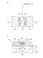
(第1の実施形態)
図1(a), (b)は、第1の実施形態において、炭化珪素層を用いた一般的な縦型蓄積型MOSFETの2つのユニットセルの結合部を示す断面図である。ここで、図1(a)は、MOSFETの電極の一部を上方から見た平面図であり、図1(b)は、図1(a)のI−I線における断面図である。
(First embodiment)
FIGS. 1A and 1B are cross-sectional views showing a coupling portion between two unit cells of a general vertical storage MOSFET using a silicon carbide layer in the first embodiment. Here, FIG. 1A is a plan view of a part of the electrode of the MOSFET as viewed from above, and FIG. 1B is a cross-sectional view taken along line I-I in FIG.
図1(a), (b)に示すように、本実施形態の半導体装置は、n+ 型の4H−SiC(0001)の半導体基板11を有している。半導体基板11は、<11−20>方向に約8度オフカットした表面を有しており、その抵抗率は約0.02Ωcm2である。半導体基板11の上には、4H−SiC(0001)のn型炭化珪素層12が設けられている。その厚さは約15μmであり、濃度3x1015cm-3の窒素がドープされている。n型炭化珪素層12は、半導体基板11の上にエピタキシャル成長により形成されたものであり、n型炭化珪素層12の上面も、半導体基板11の影響を受けて<11−20>方向にオフ角を有している。
As shown in FIGS. 1A and 1B, the semiconductor device of this embodiment includes an n + -
n型炭化珪素層12の上部のうち2つのユニットセルの結合部の両側方に位置する領域には、p型のウェル領域13が設けられている。p型ウェル領域13は、例えばアルミニウムが約2×1018cm-3の濃度で0.8μm程度の深さだけ注入した後に、約1700度の高温でアニールすることにより形成する。
A p-
n型炭化珪素層12のうち2つのp型ウェル領域に挟まれる領域の上から、その2つのp型ウェル領域の上に延びるように、n型4H−SiCからなるチャネル層14が形成されている。ここでは、チャネル層14は、アンドープ層と約5x10¹⁷Cm-3のn型不純物を含むドープ層とを交互に積層したデルタドープ層である。チャネル層14の厚さは約0.2μmとなる。
A
p型ウェル領域13の上部にはソース領域15が形成されている。ソース領域15は、チャネル層14の外側方と接するように設けられている。ソース領域15は、例えば、窒素が約1x1019cm-3の濃度で0.3μm程度の深さだけ注入した後に、約1700度の高温でアニールすることにより形成する。
A
基本的には、ソース領域15は、p型ウェル領域の一部にn型不純物を注入することにより形成され、MOSFET10は、いわゆる二重注入型のMOSFET(DIMOSFET)である。 また、図1においては、ソース領域はチャネル層を挟んだ構成となっており、p型ウェル領域を形成した上からチャネル層を堆積し、さらにチャネル層の上からn型不純物注入を行うことでソース領域を形成するが、例えばp型ウェル領域とソース領域を形成した後にチャネル層を形成したような半導体素子であっても構わない。
Basically, the
チャネル層14の上からソース領域15の一部の上には、厚さ約60nmのゲート絶縁膜16が設けられている。ゲート絶縁膜16は、ソース領域15およびチャネル層14の上部を熱酸化した後、V族元素を含む雰囲気下で熱処理することにより形成される。この熱処理の方法については後述する。
A
ゲート絶縁膜16の上には、アルミニウムからなるゲート電極17が設けられている。
On the
ソース領域15の上から、n型炭化珪素層12のうちソース領域15の外側方に位置する部分の上に亘って、ニッケルからなるソース電極18が設けられている。ソース電極18は、ニッケル膜を形成した後に約1000度の温度で熱処理することにより形成する。この熱処理により、ソース電極18とソース領域15とはオーム接触となる。ソース電極18は、p型ウェル領域13に電気的に接続されるベース電極としての役割を兼ね備えた構造を有している。ここで、ソース電極18とp型ウェル領域13との間の電気抵抗を低減するために、p型ウェル領域13のうち界面に位置する部分に、他の領域よりも高い濃度のアルミニウムをイオン注入してp+形のイオン注入領域を形成していてもよい。
A
半導体基板11の裏面上には、ニッケルからなるドレイン電極19が設けられている。ドレイン電極19は、ニッケル膜を形成した後に約1000度の温度で熱処理することにより形成する。この熱処理により、ドレイン電極19と半導体基板11とはオーム接触となる。
A
ゲート電極17の上は層間絶縁膜1Aに覆われており、層間絶縁膜1Aおよびソース電極18の上は、上部配線電極1Bに覆われている。
The
本実施形態のMOSFET10をONの状態にするためには、ドレイン電極19にプラスの電圧を印加し、ソース電極18を接地し、ゲート電極17にプラスの電圧を印加する。これにより、MOSFET10のスイッチング動作が可能となる。
In order to turn on the
MOSFET10がONの状態になると、キャリアである電子は、図1(a), (b)に示すように、まず、基板面に平行な方向に流れる。ここで、本実施形態では、オフカット方向Aに対して平行な方向に電子が流れる点が従来と異なる。その後に、電子は、図1(b)に示すように、基板面に垂直な方向に流れる。なお、図1(a), (b)に示す矢印は、キャリアである電子の進む方向を示しており、電流は、この矢印と逆の向きに流れる。
When the
ここで、ゲート絶縁膜16を形成した後に熱処理を行う方法について、図面を参照しながら詳細に説明する。なお、この方法は、本出願人による先願の特願2003−350244および特願2004−271321に記載された発明であり、本明細書では、上記出願の内容を援用することとする。
Here, a method of performing heat treatment after forming the
図2(a)〜(c)は、SiC−酸化物積層体を形成する手順を示す断面図である。本実施形態においては、V族元素として窒素を用いるが、リン(P),砒素(As)等の他のV族元素を用いてもよい。 FIGS. 2A to 2C are cross-sectional views showing a procedure for forming a SiC-oxide stack. In this embodiment, nitrogen is used as the group V element, but other group V elements such as phosphorus (P) and arsenic (As) may be used.
まず、図2(a)に示す工程で、4H−SiC(0001)基板であるSiC基板20を準備する。SiC基板20の上部(同図に示す破線よりも上方の部分)は、エピタキシャル成長により形成された4H−SiC(0001)層である。そして、SiC基板20(エピタキシャル成長されたSiC層)の主面は、MCP(メカノケミカル研磨)によって、凹凸(最大表面粗さRmax)が10nm以下になるように平滑化される。ただし、この平滑化処理は必ずしも必要ではない。
First, in the step shown in FIG. 2A, a
次に、図2(b)に示す工程で、SiC基板20をチャンバ30内に設置して、酸化性雰囲気下でSiC基板20を加熱することにより、SiC基板20上に、平均厚さ約60nmの酸化物層21(主としてSiO2を含む層)を形成する。この場合、酸化温度は1000℃以上であり、好ましくは1050℃〜1300℃である。酸化性雰囲気を生じさせるためには、チャンバ30内に、酸素,水蒸気のうち少なくともいずれか1つを含むガスを流せばよい。その後、不活性ガス(Ar,N2,He,Ne等)雰囲気中で、1000℃以上の温度(例えば、1000℃〜1150℃)でアニールする。このアニール処理によって、酸化物層21が前もって緻密化される。
Next, in the step shown in FIG. 2B, the
次に、図2(c)に示す工程で、SiC基板20を、除害装置(図示せず)及び減圧装置である真空ポンプ31が付設されたチャンバ30内に移動させて、チャンバ30内を真空ポンプ31によって約150Torr(2.0×10⁴Pa)に減圧しつつ、チャンバ30内に流量500(ml/min)のNOガス(又は、リン(P)などの窒素以外のV族元素含有ガス)を流し、チャンバ30内を窒素(N)(又は窒素以外のV族元素)が酸化物層11中に拡散するのに十分に高い温度(約1150℃)に加熱する。このとき、減圧下で、酸化物層21を窒素などのV族元素を含むガスに暴露することにより、酸化物層21内に窒素などのV族元素が拡散し、比誘電率が大きく、より緻密なV族元素含有酸化物層22が形成される。暴露は、緻密なV族元素含有酸化物層22を形成するのに充分な、そして、V族元素含有酸化物層22の特性が改良となるのに充分な時間(例えば1Hr)行なう。以上の工程により、熱処理が終了する。
Next, in the step shown in FIG. 2C, the
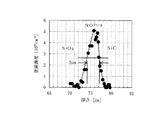
図3は、本実施形態の製造方法によって形成されたV族元素含有酸化物層22の厚さ方向における窒素濃度プロファイルをSIMSにより実測した結果を示すグラフ図である。なお、図3では、窒素濃度のピーク部(SiO2−SiC界面付近の領域)の濃度分布を抜き出して示している。同図に示すデータは、SiO2−SiC界面での窒素をCsN147で定量して得られたものである。同図に示すように、このピーク部の半値幅は3nmであり、非常に狭い領域に窒素が集中的に高濃度で導入されていることがわかる。
FIG. 3 is a graph showing the results of actually measuring the nitrogen concentration profile in the thickness direction of the group V element-containing
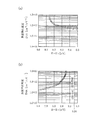
図4(a), (b)は、図3に示すデータに基づいて、High-Low法で計算した界面準位密度を示す図である。図4(a), (b)において、横軸は価電子帯Evとのポテンシャル差(E−Ev(eV))を表し、縦軸は界面準位密度Dit(cm-2eV-1)を表している。MOSFETにおけるキャリアが電子である場合には、トラップとして作用する界面準位は伝導帯端付近のポテンシャル範囲(E−Ev=2.95eV〜3.05eV)の界面準位であり、キャリアがホールである場合には、ホールトラップとして作用する界面準位は価電子帯端付近のポテンシャル範囲(E−Ev=0.3eV〜0.4eV)の界面準位であるが、図4(a), (b)に示すように、本実施形態においては、各バンド端付近のポテンシャル範囲において1×1012cm-2・eV-1以下の界面準位密度が得られている。また、V族元素含有酸化物層22全体における窒素の平均濃度は、8.3×1019cm-3 である。
4A and 4B are diagrams showing the interface state density calculated by the High-Low method based on the data shown in FIG. 4A and 4B, the horizontal axis represents the potential difference (E-Ev (eV)) from the valence band Ev, and the vertical axis represents the interface state density Dit (cm -2 eV -1 ). Represents. When the carrier in the MOSFET is an electron, the interface state acting as a trap is an interface state in the potential range (E-Ev = 2.95 eV to 3.05 eV) near the conduction band edge, and the carrier is a hole. In some cases, the interface state acting as a hole trap is an interface state in the potential range near the valence band edge (E-Ev = 0.3 eV to 0.4 eV). As shown in b), in this embodiment, an interface state density of 1 × 10 12 cm −2 · eV −1 or less is obtained in the potential range near each band edge. The average nitrogen concentration in the entire group V element-containing
このように、V族元素含有酸化物層22に窒素等のV族元素を含めることにより、キャリアのトラップとなる界面準位密度を低減させることができ、キャリア移動度の向上を図ることができる。
In this manner, by including a group V element such as nitrogen in the group V element-containing
特に、V族元素含有酸化物層22の下部における窒素濃度の最大値が、1×1020cm-3以上で1×1022cm-3以下であることにより、比誘電率の向上作用と、界面準位密度の低減作用とが顕著に得られる。
In particular, the maximum value of the nitrogen concentration in the lower portion of the V group element-containing
次に、本実施形態の半導体素子の配置について、従来と比較しながら説明する。 Next, the arrangement of the semiconductor elements according to the present embodiment will be described in comparison with the prior art.
従来では、図14に示すように、基板の上面にはステップバンチングが形成されている。このステップバンチングは、層内にイオン注入された不純物を活性化するための高温熱処理の影響で生じた。ステップバンチングは、オフカット方向に対して垂直な方向に形成されるため、従来では、オフカット方向に垂直な方向により多くのキャリアが流れるように電極等の配置を決定していた。 Conventionally, step bunching is formed on the upper surface of the substrate as shown in FIG. This step bunching occurred due to the effect of high temperature heat treatment to activate the impurities implanted into the layer. Since step bunching is formed in a direction perpendicular to the offcut direction, the arrangement of electrodes and the like has been conventionally determined so that more carriers flow in the direction perpendicular to the offcut direction.
それに対し、本実施形態では、オフカット方向にほぼ平行により多くのキャリアが流れるように素子を配置している。図5は、図1に示す半導体装置において、キャリアの移動する方向と素子の配置との関係を示す平面図である。図5では、ゲート電極17およびソース電極18等の図示を省略し、n型炭化珪素層12、p型ウェル領域13およびn型ソース領域15のみを示している。チャネル層14の図示は省略しているが、チャネル層14は、p型ウェル領域13のうち斜線を付して示す領域の上に位置している。図5に示すように、縦型のMOSFETでは、キャリアが、ソース領域15からn型炭化珪素層12の方に向かって流れる。この方向がオフカット方向Aとほぼ平行になるように素子を配置する。
On the other hand, in this embodiment, the elements are arranged so that more carriers flow almost in parallel with the off-cut direction. FIG. 5 is a plan view showing the relationship between the carrier moving direction and the element arrangement in the semiconductor device shown in FIG. In FIG. 5, illustration of the
−オフカット方向において電子移動度が大きくなる原理−
従来の半導体素子は、オフカット方向に平行な方向よりも垂直な方向の方が電子移動度が大きいという異方性を有していた。それに対し、本実施形態の半導体装置ではこの異方性が逆転している。これは、本実施形態では、窒素と酸素とを含むガスを用いた熱処理を行うことにより、炭化珪素層とゲート絶縁膜の界面における界面準位密度が低下し、オフカット方向に沿った方向の電子移動度が向上する。以下に、炭化珪素基板の電子移動度が、オフカット方向において大きいという理由について考察する。
-Principle of increasing electron mobility in the off-cut direction-
The conventional semiconductor element has anisotropy that the electron mobility is higher in the direction perpendicular to the direction parallel to the offcut direction. On the other hand, this anisotropy is reversed in the semiconductor device of this embodiment. This is because, in this embodiment, by performing a heat treatment using a gas containing nitrogen and oxygen, the interface state density at the interface between the silicon carbide layer and the gate insulating film is reduced, and the direction along the offcut direction is reduced. Electron mobility is improved. Hereinafter, the reason why the electron mobility of the silicon carbide substrate is large in the off-cut direction will be considered.
図6(a)は、(0001)面を上面とする炭化珪素基板において、電子の移動する向きと大きさをベクトルにして示す図である。図6(a)では、(0001)面(指定された結晶面S)および紙面に平行なベクトルをaベクトル、(0001)面に平行であって紙面に垂直なベクトルをbベクトル、(0001)面に垂直なベクトルをcベクトルとしている。 FIG. 6A is a diagram showing the direction and magnitude of electrons as vectors in a silicon carbide substrate having the (0001) plane as an upper surface. In FIG. 6A, a vector parallel to the (0001) plane (designated crystal plane S) and the plane of the paper is a vector, a vector parallel to the (0001) plane and perpendicular to the plane of the paper is the b vector, (0001) A vector perpendicular to the plane is set as c vector.
ここで、(0001)面を上面とする炭化珪素層においては、電子移動度は、基板面内方向よりも基板面に対して垂直な方向で大きくなる。つまり、図6(a)に示すcベクトルの方が、ベクトルaおよびベクトルbよりも大きい。また、aベクトルとbベクトルとは同じ大きさとなる。 Here, in the silicon carbide layer having the (0001) plane as the upper surface, the electron mobility is larger in the direction perpendicular to the substrate surface than in the substrate in-plane direction. That is, the c vector shown in FIG. 6A is larger than the vector a and the vector b. Further, the a vector and the b vector have the same size.
次に、炭化珪素基板がオフカット基板の場合を考える。図6(b)は、(0001)面に対して角度θだけ傾いた面を上面とする炭化珪素基板において、電子の移動する向きと大きさをベクトルにして示す図である。 Next, consider the case where the silicon carbide substrate is an off-cut substrate. FIG. 6B is a diagram showing, in the form of a vector, the direction and magnitude of electrons in a silicon carbide substrate having a surface inclined by an angle θ with respect to the (0001) plane.
図6(b)では、aベクトルおよびcベクトルを、オフカット方向とオフカット方向に垂直な方向とに分解して、それぞれ、a1, a2, c1, c2ベクトルとして示す。このとき、オフカット方向の電子移動度を表すベクトルをdベクトルとすると、dベクトルは、a1ベクトルとc1ベクトルとの和で表される。 In FIG. 6B, the a vector and the c vector are decomposed into an offcut direction and a direction perpendicular to the offcut direction, and are shown as a1, a2, c1, and c2 vectors, respectively. At this time, if a vector representing the electron mobility in the offcut direction is a d vector, the d vector is represented by the sum of the a1 vector and the c1 vector.
ここで、cベクトルはaベクトルよりも大きいので、dベクトルはaベクトルより大きくなる。それに対し、bベクトルはオフカット方向に対して垂直であるため、炭化珪素層の上面が(0001)面であっても、オフカット面であっても、その方向の電子移動度の大きさは変化しない。aベクトルとbベクトルとは同じ大きさであるから、dベクトルとbベクトルの大きさを比べると、明らかにdベクトルの方が大きくなる。 Here, since the c vector is larger than the a vector, the d vector is larger than the a vector. On the other hand, since the b vector is perpendicular to the offcut direction, the magnitude of the electron mobility in that direction is the same regardless of whether the upper surface of the silicon carbide layer is the (0001) plane or the offcut plane. It does not change. Since the a vector and the b vector have the same size, the d vector is clearly larger when the sizes of the d vector and the b vector are compared.
以上のことから、オフカット基板において、オフカット方向の電子移動度(ベクトルd)は、オフカット方向に垂直な方向の電子移動度(ベクトルb)よりも大きくなる。 From the above, in the offcut substrate, the electron mobility (vector d) in the offcut direction is larger than the electron mobility (vector b) in the direction perpendicular to the offcut direction.
もちろん、オフカット基板面内において、bベクトルとdベクトル以外の方向のベクトルを考慮しても、オフカット基板面内ではオフカット方向の電子移動度が一番大きくなることは明白である。 Of course, it is obvious that the electron mobility in the off-cut direction is the largest in the off-cut substrate plane even if vectors in directions other than the b vector and the d vector are taken into consideration in the off-cut substrate plane.
以上のベクトルの効果、および、窒素と酸素とを含むガスを用いた熱処理を行うことによる炭化珪素層/ゲート絶縁膜界面の界面準位密度低下効果の相乗効果により、オフカット方向に沿った方向の電子移動度が向上する。 The direction along the off-cut direction due to the synergistic effect of the above-described vector effect and the effect of lowering the interface state density at the silicon carbide layer / gate insulating film interface by performing the heat treatment using a gas containing nitrogen and oxygen. The electron mobility of is improved.
−電極の配置例−
図1に示す2つのユニットセルの結合部では、オフカット方向Aに平行な方向にのみ電流を流す例を示した。しかし実際には、縦型の半導体素子では複数の方向に電流を流す場合が多い。この場合には、複数の方向の中で最も電流量の多い方向がオフカット方向と平行になるように素子を配置する。以下に、その構造について説明する。
-Example of electrode arrangement-
In the connection part of the two unit cells shown in FIG. However, in reality, a vertical semiconductor element often passes current in a plurality of directions. In this case, the elements are arranged so that the direction with the largest amount of current among the plurality of directions is parallel to the off-cut direction. The structure will be described below.
(第1の配置例)
縦型のMOSFETにおいては、ソース電極18およびゲート電極17がストライプ状(または櫛形)に配置されている場合がある。そのような場合について、図7(a), (b)を参照しながら説明する。
(First arrangement example)
In the vertical MOSFET, the
図7(a), (b)は、ゲート電極およびソース電極が櫛形の形状で配置される場合の構造を示す図である。図7(a)はゲート電極17およびソース電極18の配置を示し、図7(b)は、n型炭化珪素層12、p型ウェル領域13およびn型ソース領域15の配置を示している。図7(a)に示すように、ソース電極17では、複数の矩形部がストライプ状に配置し、矩形部のうちの一端は、矩形部の伸びる方向とは垂直な方向に伸びる接続部に接することにより互いに電気的に接続されている。また、ゲート電極17においても、複数の矩形部が、ソース電極17における矩形部と交互にストライプ状に配置し、矩形部のうちの一端は、矩形部の伸びる方向とは垂直な方向に伸びる接続部に接することにより互いに電気的に接続されている。チャネル領域は、図7(b)の斜線で示す領域に配置している。この場合には、キャリアの移動する方向は方向Aと方向Bとの2通りある。そして、チャネル領域は、主に方向Aに対して垂直な方向に延びている。つまり、チャネル領域において、方向Aに沿う電流を流すチャネル領域の幅W1が、その他の方向のチャネル領域の幅W2以上となるように素子を構成する。また、n型ソース領域15の最も長い辺も、オフカット方向Aに垂直な方向に配置している。
FIGS. 7A and 7B are diagrams showing a structure when the gate electrode and the source electrode are arranged in a comb shape. FIG. 7A shows the arrangement of the
(第2の配置例)
縦型のMOSFETは、多角形のユニットセルごとに配置され、各ユニットセルでは、ソース電極の側方がゲート電極によって囲まれている場合がある。そのような場合について、図8(a), (b)を参照しながら説明する。
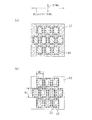
(Second arrangement example)
The vertical MOSFET is arranged for each polygonal unit cell, and in each unit cell, the side of the source electrode may be surrounded by the gate electrode. Such a case will be described with reference to FIGS. 8 (a) and 8 (b).
図8(a), (b)は、四角形のユニットセルが配置される場合の構造を示す図である。図8(a)はゲート電極17およびソース電極18の配置を示し、図8(b)は、n型炭化珪素層12、p型ウェル領域13およびn型ソース領域15の配置を示している。チャネル領域は、図8(b)の斜線で示す領域に配置している。
FIGS. 8A and 8B are diagrams showing a structure in the case where square unit cells are arranged. FIG. 8A shows the arrangement of the
この場合には、キャリアの移動する方向は、主に方向Aと方向Bとの2通りある。そして、ユニットセルの長手方向を方向Aに対して垂直に配置すると、方向Aに対して垂直な方向に延びるチャネル領域の方が平行な方向にのびるチャネル領域よりも長くなる。つまり、図8(b)に示すように、チャネル領域において、方向Aに沿う電流を流すチャネル領域の幅W1が、その他の方向のチャネル領域の幅W2以上となるように素子を構成する。また、n型ソース領域15の最も長い辺も、オフカット方向Aに垂直な方向に配置している。
In this case, there are mainly two directions in which the carrier moves, ie, direction A and direction B. When the longitudinal direction of the unit cell is arranged perpendicular to the direction A, the channel region extending in the direction perpendicular to the direction A is longer than the channel region extending in the parallel direction. That is, as shown in FIG. 8B, in the channel region, the element is configured such that the width W1 of the channel region in which the current along the direction A flows is equal to or larger than the width W2 of the channel region in the other direction. The longest side of the n-
なお、ここではユニットセルが長方形の場合について説明したが、ユニットセルが平行四辺形や菱形など他の多角形であっても構わない。図9(a), (b)は、六角形のユニットセルが配置される場合の構造を示す図である。図9(a)は、ゲート電極17およびソース電極18の配置を示し、図9(b)は、n型炭化珪素層12、p型ウェル領域13およびn型ソース領域15の配置を示している。チャネル領域は、図9(b)の斜線で示す領域に配置している。
Although the case where the unit cell is rectangular has been described here, the unit cell may be another polygon such as a parallelogram or a rhombus. FIGS. 9A and 9B are diagrams showing the structure when hexagonal unit cells are arranged. 9A shows the arrangement of the
この場合には、キャリアの移動する方向は、主に方向A、方向Cおよび方向Dの3通りある。そして、六角形のユニットセルの辺のうち最も長い辺を方向Aに対して垂直に配置すると、方向Aに対して垂直な方向に延びるチャネル領域が、方向Cや方向Dに対して垂直な方向に伸びるチャネル層よりも長くなる。つまり、図9(b)に示すように、チャネル領域において、方向Aに沿う電流を流すチャネル領域の幅W1が、その他の方向のチャネル領域の幅W2以上となるように素子を構成する。また、n型ソース領域15の最も長い辺も、オフカット方向Aに垂直な方向に配置している。
In this case, there are mainly three directions of carrier movement: direction A, direction C, and direction D. When the longest side of the hexagonal unit cell sides is arranged perpendicular to the direction A, the channel region extending in the direction perpendicular to the direction A becomes a direction perpendicular to the direction C or the direction D. It becomes longer than the channel layer extending. That is, as shown in FIG. 9B, in the channel region, the element is configured such that the width W1 of the channel region in which the current along the direction A flows is equal to or larger than the width W2 of the channel region in the other direction. The longest side of the n-
なお、本実施形態で述べた方法は、チャネル層としてデルタドープ層を有する場合だけでなく、チャネル層が通常のn型不純物層である場合にも適用できる。 Note that the method described in this embodiment can be applied not only when the channel layer includes a delta doped layer but also when the channel layer is a normal n-type impurity layer.
また、本実施形態で述べた方法は縦型反転型MOSFET60にも適用できる。図10は、縦型反転型MOSFETの構造を示す断面図である。図10のうち図1と異なる点は、チャネル層14(図1に示す)が形成されていない点である。その他の構造は図1と同様であるので説明を省略する。
The method described in this embodiment can also be applied to the
(第2の実施形態)
図11(a), (b)は、第2の実施形態において、炭化珪素層を用いた一般的な横型蓄積型MOSFETを示す断面図である。ここで、図11(a)は、MOSFETの電極の一部を上方から見た平面図であり、図11(b)は、図11(a)のVII−VII線における断面図である。
(Second Embodiment)
FIGS. 11A and 11B are cross-sectional views showing a general lateral accumulation type MOSFET using a silicon carbide layer in the second embodiment. Here, FIG. 11A is a plan view of a part of the electrode of the MOSFET as viewed from above, and FIG. 11B is a cross-sectional view taken along the line VII-VII in FIG.
図11(a), (b)に示すように、本実施形態の半導体装置は、半絶縁性の4H−SiC(0001)の半導体基板71を有している。半導体基板71は、<11−20>方向に約8度オフカットした表面を有している。半導体基板71の上には、4H−SiC(0001)のp型炭化珪素層72が設けられている。その厚さは約5μmであり、濃度5×1015cm-3のアルミニウムがドープされている。
As shown in FIGS. 11A and 11B, the semiconductor device of this embodiment includes a semi-insulating 4H—SiC (0001)
p型炭化珪素層72の上部のうちの中央部には、n型のチャネル層74が設けられている。ここでは、チャネル層74は、アンドープ層と、約5x10¹⁷Cm-3のn型不純物を含むドープ層とを交互に積層したデルタドープ層であるとする。チャネル層74の厚さは約0.2μmとなる。
An n-
p型炭化珪素層72のうちチャネル層74の両側方に位置する領域には、ソース領域75sおよびドレイン領域75dが設けられている。ソース領域75sおよびドレイン領域75dは、例えば、窒素を約1x1019cm-3の濃度で0.3μm程度の深さだけ注入した後に、約1700度の高温でアニールすることにより形成する。
A
基本的には、ソース領域75sおよびドレイン領域75dは、p型ウェル領域の一部にn型不純物を注入することにより形成され、MOSFET70は、いわゆる二重注入型のMOSFET(DIMOSFET)である。
Basically, the
また、図11(a), (b)においては、ソース領域とドレイン領域がチャネル層を挟んだ構成となっており、p型ウェル領域を形成した上からチャネル層を堆積し、さらにチャネル層の上からn型不純物注入を行うことでソース領域とドレイン領域を形成するが、例えばp型ウェル領域とソース領域およびドレイン領域を形成した後にチャネル層を形成したような半導体素子であっても構わない。 Further, in FIGS. 11A and 11B, the source region and the drain region have a structure in which the channel layer is sandwiched. The channel layer is deposited after the p-type well region is formed, and the channel layer is further formed. The source region and the drain region are formed by performing n-type impurity implantation from the top. For example, a semiconductor element in which a channel layer is formed after the p-type well region, the source region, and the drain region are formed may be used. .
チャネル層74の上からソース領域75sおよびドレイン領域75dのうちの端部の上に亘って、厚さ約60nmのゲート絶縁膜76が設けられている。ゲート絶縁膜76は、チャネル層74、ソース領域75sおよびドレイン領域75dの上部を熱酸化した後に、V族元素を含む雰囲気下で熱処理することにより形成される。
A
ゲート絶縁膜76の上には、アルミニウムからなるゲート電極77が設けられている。
On the
ソース領域75sの上にはニッケルからなるソース電極78が設けられ、ドレイン領域75dの上にはニッケルからなるドレイン電極79が設けられている。ソース電極78およびドレイン電極79は、ニッケル膜を形成した後に約1000度の温度で熱処理することにより形成する。この熱処理により、ソース領域75sとソース電極78およびドレイン領域75dとドレイン電極79とは、それぞれオーム接触となる。
A
p型炭化珪素層72のうちソース領域75sの外側方に位置する領域の上には、ベース電極7Cが設けられている。ベース電極7Cは、p型炭化珪素層72を外部と電気的に接続するために設けられている。ベース電極7Cとp型炭化珪素層72との間の電気抵抗を低減するために、p型炭化珪素層72のうち界面に位置する部分に、他の領域よりも高い濃度のアルミニウムをイオン注入してp+型のイオン注入領域を形成していてもよい。また、ソース電極78とベース電極7Cとが、電気的に接合されていてもよいし、同一の導体膜からなっていてもよい。
A base electrode 7 </ b> C is provided on a region of p-type
本実施形態のMOSFET70をONの状態にするためには、ドレイン電極79にプラスの電圧を印加し、ソース電極78およびベース電極7Cを接地し、ゲート電極77にプラスの電圧を印加する。これにより、MOSFET70のスイッチング動作が可能となる。
In order to turn on the
MOSFET70がONの状態になると、キャリアである電子は、図11(a), (b)に示すように、ソース領域75sからドレイン領域75dの方に向かって、基板面にほぼ平行に流れる。ここで、本実施形態では、オフカット方向Aに対して平行な方向に電子が流れる点が従来と異なる。以下に、本実施形態の半導体素子の配置について、図12を参照しながら説明する。図12は、図11(b)に示す半導体装置において、キャリアの移動する方向と素子の配置との関係を示す平面図である。図12では、ゲート電極77、ソース電極78およびドレイン電極79等の図示を省略し、p型炭化珪素層72、n型ソース領域75sおよびn型ドレイン領域75dのみを示している。チャネル層74の図示は省略しているが、チャネル層74は、p型炭化珪素層72のうち斜線を付して示す領域の上に位置している。図12に示すように、横型のMOSFETでは、キャリアが、ソース領域75sからドレイン領域75dの方に向かって流れる。この方向がオフカット方向Aとほぼ平行になるように素子を配置する。
When the
横型素子において流れる電流の方向は1方向である場合が多い。横型素子においても、電流方向が1方向だけでない場合もあるが、その時は、基板のオフカット方向Aに平行な方向に流れる電流が支配的となるように素子を配置する。つまり、チャネル層74の幅のうち、方向Aに沿う電流を流すチャネル領域の幅W1が、チャネル層74の幅のうち他の方向の幅以上となるように素子を配置する。いいかえると、ソース領域75sとドレイン領域75dとの辺のうち互いに対向する辺(チャネル層74と接する辺)がオフカット方向Aと垂直になるように素子を配置する。
In many cases, the direction of the current flowing in the lateral element is one direction. Even in the horizontal type element, the current direction is not limited to one direction. In this case, the element is arranged so that the current flowing in the direction parallel to the off-cut direction A of the substrate becomes dominant. In other words, the elements are arranged such that, of the width of the
なお、本実施形態で述べた方法は、チャネル層としてデルタドープ層を有する場合だけでなく、チャネル層が通常のn型不純物層である場合にも適用できる。 Note that the method described in this embodiment can be applied not only when the channel layer includes a delta doped layer but also when the channel layer is a normal n-type impurity layer.
また、本実施形態で述べた方法は横型反転型MOSFETにも適用できる。図13は、横型反転型MOSFETの構造を示す断面図である。図13のうち図11(b)と異なる点は、チャネル層74(図11(b)に示す)が形成されていない点である。その他の構造は図11(b)と同様であるので説明を省略する。 The method described in this embodiment can also be applied to a lateral inversion MOSFET. FIG. 13 is a cross-sectional view showing the structure of a lateral inversion MOSFET. 13 differs from FIG. 11B in that the channel layer 74 (shown in FIG. 11B) is not formed. Since other structures are the same as those in FIG.
(その他の実施形態)
なお、上述の実施形態においては、半導体基板として4H−SiCから約8度オフカットされた表面を有する基板を用いた。しかしながら、本発明では、指定された結晶面Sから所定の方向Aに10度以下の角度だけ傾いた表面を具備した基板であれば、他の基板を用いてもよい。
(Other embodiments)
In the above-described embodiment, a substrate having a surface that is cut off about 4 degrees from 4H—SiC is used as the semiconductor substrate. However, in the present invention, any other substrate may be used as long as the substrate has a surface inclined by an angle of 10 degrees or less in the predetermined direction A from the designated crystal plane S.
また、本発明では、例えば、オフカットされたSi基板の上にヘテロエピタキシャル成長させた炭化珪素層を用いてもよい。 In the present invention, for example, a silicon carbide layer heteroepitaxially grown on an off-cut Si substrate may be used.
また、上述の実施形態においては、4H−SiCの炭化珪素層を用いた。しかしながら、本発明では、結晶面の面内方向よりも、結晶面に対する垂直方向の方が電子移動度が大きいという性質を有している他のポリタイプの炭化珪素層を用いてもよい。 In the above-described embodiment, a 4H—SiC silicon carbide layer is used. However, in the present invention, other polytype silicon carbide layers having the property that the electron mobility is higher in the direction perpendicular to the crystal plane than in the in-plane direction of the crystal plane may be used.
ここで、結晶面の面内方向よりも結晶面に対する垂直方向の方が電子移動度が小さいという性質を有するポリタイプであっても、そのポリタイプのオフカット基板において、オフカット方向に垂直な方向よりもオフカット方向の方が電子移動度が大きくなる場合があれば、そのようなオフカット基板を用いてもかまわない。 Here, even in a polytype having a property that the electron mobility is smaller in the direction perpendicular to the crystal plane than in the in-plane direction of the crystal plane, the polytype offcut substrate is perpendicular to the offcut direction. If the electron mobility may be higher in the offcut direction than in the direction, such an offcut substrate may be used.
また、上述の実施形態では、4H−SiC(0001)基板を、<11−20>方向にオフカットした半導体基板を用いた。しかしながら、本発明では、半導体基板として、<11−20>方向、または<1−100>方向にオフカットした基板を用いてもよい。この場合に、半導体基板の上に炭化珪素層をエピタキシャル成長すると、炭化珪素層の上面は(0001)面から<11−20>方向、または<1−100>方向にオフカットした面となる。ただし、炭化珪素層の上面に所望の面が現れるのであれば、炭化珪素層の下に位置する半導体基板の面方位やオフカット方向は特に限定しない。すなわち、ソース領域のうち最も長い辺がオフカット方向に垂直な方向に沿っている構成を有していれば、上記以外のいかなるオフカット方向であってもかまわない。 Moreover, in the above-mentioned embodiment, the semiconductor substrate which cut off the 4H-SiC (0001) board | substrate in the <11-20> direction was used. However, in the present invention, a substrate cut off in the <11-20> direction or the <1-100> direction may be used as the semiconductor substrate. In this case, when the silicon carbide layer is epitaxially grown on the semiconductor substrate, the upper surface of the silicon carbide layer is a surface that is off-cut from the (0001) plane in the <11-20> direction or the <1-100> direction. However, as long as a desired surface appears on the upper surface of the silicon carbide layer, the plane orientation and the off-cut direction of the semiconductor substrate located under the silicon carbide layer are not particularly limited. That is, as long as the longest side of the source region has a configuration along the direction perpendicular to the offcut direction, any offcut direction other than the above may be used.
また、炭化珪素の(0001)面は、一般にはシリコン面を表している。しかし、本発明では、(0001)面の代わりに(000−1)面として表記されるカーボン面を用いても差し支えない。 Further, the (0001) plane of silicon carbide generally represents a silicon plane. However, in the present invention, a carbon surface represented as a (000-1) plane may be used instead of the (0001) plane.
また、炭化珪素において、オフカット方向の電子移動度がその他の方向の電子移動度より大きくなる状態は、MOSFETのチャネル領域とゲート絶縁膜との界面において、炭化珪素の伝導体の準位より0.1eV小さい準位における界面準位密度が5x1012cm-2・eV-1以下である場合に実現できる。より好ましくは、上記の界面における界面準位密度は1x1012cm-2・eV-1以下とする。逆に、界面準位密度が5x1012cm-2・eV-1より大きい場合には、上記界面に発生するステップバンチングの影響を受けて、従来の炭化珪素半導体素子のようにオフカット方向(ステップバンチングに対して垂直な方向)の電子移動度はステップバンチングに対して平行な方向の電子移動度より小さくなる。 In silicon carbide, the state in which the electron mobility in the off-cut direction is larger than the electron mobility in the other direction is 0 from the level of the silicon carbide conductor at the interface between the channel region of the MOSFET and the gate insulating film. This can be realized when the interface state density at a level of 0.1 eV is 5 × 10 12 cm −2 · eV −1 or less. More preferably, the interface state density at the interface is 1 × 10 12 cm −2 · eV −1 or less. On the contrary, when the interface state density is larger than 5 × 10 12 cm −2 · eV −1 , under the influence of step bunching generated at the interface, the off-cut direction (step) is reduced as in the conventional silicon carbide semiconductor device. The electron mobility in the direction perpendicular to the bunching is smaller than the electron mobility in the direction parallel to the step bunching.
また、上述の実施形態では、炭化珪素層とゲート絶縁膜との間の界面における界面準位密度を低減するために、ゲート絶縁膜を形成した後に酸化窒素(NO)を含む雰囲気下で熱処理を行った。しかし、本発明では、酸化窒素(NO)に限らず、V族元素を含む雰囲気で熱処理することにより、同様の効果を得ることができる。また、界面準位密度を低減できるのであれば、他の雰囲気で熱処理を行ってもよいし、他の処理方法を行ってもよい。 In the above-described embodiment, in order to reduce the interface state density at the interface between the silicon carbide layer and the gate insulating film, the heat treatment is performed in an atmosphere containing nitrogen oxide (NO) after forming the gate insulating film. went. However, in the present invention, similar effects can be obtained by heat treatment in an atmosphere containing a group V element, not limited to nitrogen oxide (NO). Further, if the interface state density can be reduced, heat treatment may be performed in another atmosphere, or another treatment method may be performed.
また、上述の実施形態では、電極材料としてニッケルやアルミニウムを用いたが、本発明では、電極材料はそれらの材料に限定されるものではないし、電極を積層構造にしていてもかまわない。 In the above embodiment, nickel or aluminum is used as the electrode material. However, in the present invention, the electrode material is not limited to these materials, and the electrode may have a laminated structure.
また、本発明の炭化珪素半導体素子の製造方法においては、実施の形態で示した製造方法以外の方法であってももちろんかまわないし、特に指定しない限り、説明に用いたプロセスの条件やガス種に制限されることはなく、他の条件であってももちろんかまわない。 In addition, in the method for manufacturing a silicon carbide semiconductor element of the present invention, a method other than the manufacturing method shown in the embodiment may of course be used. Unless otherwise specified, the process conditions and gas types used in the description are not limited. There is no limitation, and other conditions may be used.
もちろん、本発明の炭化珪素半導体素子においては、発明の範囲内における基本構造が異ならない限りの種々の変形が可能である。 Of course, the silicon carbide semiconductor element of the present invention can be variously modified as long as the basic structure does not differ within the scope of the invention.
本発明の半導体素子は、ステップバンチングやその他の良好でない界面状態によって低下した炭化珪素層の電子移動度が改善されるため高い電気特性を得ることができる点で産業上の利用可能性は高い。 The semiconductor device of the present invention has high industrial applicability in that high electrical characteristics can be obtained because the electron mobility of the silicon carbide layer, which has been lowered by step bunching and other poor interface states, is improved.
1A 層間絶縁膜
1B 上部配線電極
7C ベース電極
10 縦型蓄積型MOSFET
11 半導体基板
12 n型炭化珪素層
13 p型ウェル領域
14 チャネル層
15 n型ソース領域
16 ゲート絶縁膜
17 ゲート電極
18 ソース電極
19 ドレイン電極
20 SiC基板
21 酸化物層
30 チャンバ
31 真空ポンプ
60 縦型反転型MOSFET
70 横型蓄積型MOSFET
71 半導体基板
72 p型炭化珪素層
74 チャネル層
75d ドレイン領域
75s ソース領域
76 ゲート絶縁膜
77 ゲート電極
78 ソース電極
79 ドレイン電極
90 横型反転型MOSFET
101 半導体基板
102 n型炭化珪素層
103 p型ウェル領域
104 チャネル層
105 ソース領域
106 ゲート絶縁膜
107 ゲート電極
108 ソース電極
109 ドレイン電極
1A Interlayer insulation film
1B Upper wiring electrode
7C base electrode
10 Vertical storage MOSFET
11 Semiconductor substrate
12 n-type silicon carbide layer
13 p-type well region
14 Channel layer
15 n-type source region
16 Gate insulation film
17 Gate electrode
18 Source electrode
19 Drain electrode
20 SiC substrate
21 Oxide layer
30 chambers
31 Vacuum pump
60 Vertical Inverted MOSFET
70 Horizontal Storage MOSFET
71 Semiconductor substrate
72 p-type silicon carbide layer
74 channel layer
75d drain region
75s source area
76 Gate insulation film
77 Gate electrode
78 Source electrode
79 Drain electrode
90 Horizontal Inverted MOSFET
Claims (31)
上記半導体基板の上に設けられ、結晶面から10度以下の角度だけオフカット方向に傾いた上面を有する炭化珪素層と、
上記炭化珪素層の上に設けられたゲート絶縁膜と、上記ゲート絶縁膜の上に設けられたゲート電極と、
上記炭化珪素層の上のうち上記ゲート電極の側方に設けられたソース電極と、
上記半導体基板の下方に設けられたドレイン電極と、
上記炭化珪素層のうち少なくとも上記ソース電極の下に位置する領域に設けられたソース領域とを備え、
平面視して、上記ソース領域のうち最も長い辺は、上記オフカット方向に垂直な方向に沿っている、半導体素子。 A semiconductor substrate;
A silicon carbide layer provided on the semiconductor substrate and having an upper surface inclined in an off-cut direction by an angle of 10 degrees or less from a crystal plane;
A gate insulating film provided on the silicon carbide layer, a gate electrode provided on the gate insulating film,
A source electrode provided on a side of the gate electrode on the silicon carbide layer;
A drain electrode provided below the semiconductor substrate;
A source region provided at least in a region located below the source electrode of the silicon carbide layer,
A semiconductor element, wherein the longest side of the source region is along a direction perpendicular to the off-cut direction in plan view.
上記炭化珪素層のうち上記ソース領域の側方および下方に設けられた第2導電型のウェル領域と、
上記ウェル領域と電気的に接続されるベース電極とをさらに備える、半導体素子。 The semiconductor device according to claim 1,
A second conductivity type well region provided laterally and below the source region of the silicon carbide layer;
A semiconductor device further comprising a base electrode electrically connected to the well region.
上記オフカット方向に垂直な方向に沿った方向とは、上記オフカット方向に垂直な方向からの傾きが5度以内の方向である、半導体素子。 The semiconductor element according to claim 1 or 2,
The direction along the direction perpendicular to the off-cut direction is a semiconductor element whose inclination from the direction perpendicular to the off-cut direction is within 5 degrees.
上記炭化珪素層のうち上記ゲート絶縁膜の下に位置する領域にチャネル層が設けられている、半導体素子。 It is a semiconductor element given in any 1 paragraph among Claims 1-3,
A semiconductor element, wherein a channel layer is provided in a region of the silicon carbide layer located under the gate insulating film.
上記チャネル領域には、少なくとも1層の第1炭化珪素層と、第1炭化珪素層よりも第1導電型の不純物濃度が高くかつ第1炭化珪素層の膜厚よりも薄い、少なくとも1層の第2炭化珪素層とを有する積層構造が設けられている、半導体素子。 The semiconductor device according to claim 4,
The channel region includes at least one first silicon carbide layer and at least one layer having a first conductivity type impurity concentration higher than that of the first silicon carbide layer and less than the thickness of the first silicon carbide layer. A semiconductor element provided with a laminated structure having a second silicon carbide layer.
上記炭化珪素層では、結晶面の面内方向における電子移動度よりも、上記結晶面に対する垂直方向における電子移動度の方が大きい、半導体素子。 It is a semiconductor element given in any 1 paragraph among Claims 1-5,
In the silicon carbide layer, the electron mobility in the direction perpendicular to the crystal plane is larger than the electron mobility in the in-plane direction of the crystal plane.
上記炭化珪素層は、4H−SiCである、半導体素子。 It is a semiconductor element given in any 1 paragraph among Claims 1-6,
The semiconductor element, wherein the silicon carbide layer is 4H—SiC.
上記炭化珪素層の上面は、(0001)面から<11−20>方向に傾いた面である、半導体素子。 The semiconductor element according to any one of claims 1 to 7,
The upper surface of the said silicon carbide layer is a semiconductor element which is a surface inclined in the <11-20> direction from the (0001) plane.
上記炭化珪素層の上面は、(0001)面から<1−100>方向に傾いた面である、半導体素子。 The semiconductor element according to any one of claims 1 to 7,
The upper surface of the said silicon carbide layer is a semiconductor element which is a surface inclined in the <1-100> direction from the (0001) plane.
上記ゲート絶縁膜は、上記炭化珪素層の上部を熱酸化した後に、V族元素を含む化合物
を含む雰囲気で熱処理することにより形成された、半導体素子。 It is a semiconductor element given in any 1 paragraph among Claims 1-9,
The gate insulating film is a semiconductor element formed by thermally oxidizing an upper portion of the silicon carbide layer and then performing a heat treatment in an atmosphere containing a compound containing a group V element.
上記V族元素を含む化合物は、酸化窒素である、半導体素子。 It is a semiconductor element of Claim 10, Comprising: The semiconductor element in which the compound containing the said V group element is nitric oxide.
上記炭化珪素層と上記ゲート絶縁膜との界面において、窒素濃度の最大値が1×1020cm-3以上で1×1022cm-3以下である、半導体素子。 The semiconductor element according to claim 10 or 11,
A semiconductor element having a maximum nitrogen concentration of 1 × 10 20 cm −3 or more and 1 × 10 22 cm −3 or less at an interface between the silicon carbide layer and the gate insulating film.
上記ソース電極は、上記ベース電極と同一の膜で設けられている、半導体素子。 It is a semiconductor element given in any 1 paragraph among Claims 1-12,
The semiconductor element, wherein the source electrode is formed of the same film as the base electrode.
上記ゲート電極は、平面視して多角形がくり抜かれた形状で設けられ、
上記多角形におけるくり抜かれた部分の辺のうち最も長い辺は、上記オフカット方向に垂直な方向に沿っている、半導体素子。 A semiconductor device according to any one of claims 1 to 13,
The gate electrode is provided in a shape in which a polygon is cut out in plan view,
The longest side among the sides of the hollowed portion in the polygon is a semiconductor element along a direction perpendicular to the off-cut direction.
平面視して、上記ソース電極は多角形の形状で配置し、上記ゲート電極は上記ソース電極と離間して、かつ上記ソース電極の側方を囲む形状で配置している、半導体素子。 The semiconductor device according to claim 14,
The semiconductor element, wherein the source electrode is arranged in a polygonal shape in plan view, and the gate electrode is arranged in a shape that is separated from the source electrode and surrounds the side of the source electrode.
上記ゲート電極は、平面視して多角形の形状で設けられ、
上記多角形の辺のうち最も長い辺は、上記オフカット方向に垂直な方向に沿っている、半導体素子。 A semiconductor device according to any one of claims 1 to 13,
The gate electrode is provided in a polygonal shape in plan view,
The longest side among the polygonal sides is a semiconductor element along a direction perpendicular to the off-cut direction.
平面視して、上記ソース電極は、ストライプ状に並ぶ複数の第1矩形部と、上記複数の第1矩形部の端部を接続する第1接続部とを有する櫛形に配置し、上記ゲート電極は、上記複数の第1矩形部のそれぞれと交互に配置するストライプ状の複数の第2矩形部と、上記第2矩形部の端部を接続する第2接続部とを有する櫛形に配置している、半導体素子。 The semiconductor device according to claim 16, wherein
In plan view, the source electrode is arranged in a comb shape having a plurality of first rectangular portions arranged in a stripe shape and a first connection portion connecting ends of the plurality of first rectangular portions, and the gate electrode Are arranged in a comb shape having a plurality of striped second rectangular portions alternately arranged with each of the plurality of first rectangular portions, and a second connecting portion connecting the end portions of the second rectangular portions. A semiconductor element.
上記半導体基板の上に設けられ、結晶面から10度以下の角度だけオフカット方向に傾いた上面を有する炭化珪素層と、
上記炭化珪素層の上に設けられたゲート絶縁膜と、上記ゲート絶縁膜の上に設けられたゲート電極と、
上記炭化珪素層の上のうち上記ゲート電極の側方に設けられたソース電極と、
上記炭化珪素層の上のうち上記ゲート電極の側方に設けられたドレイン電極と、
上記炭化珪素層のうち少なくとも上記ソース電極および上記ドレイン電極の下に位置する領域に互いに離間して設けられたソース・ドレイン領域とを備え、
平面視して、上記ソース・ドレイン領域の辺のうち互いに対向する辺は、上記オフカット方向に垂直な方向に沿っている、半導体素子。 A semiconductor substrate;
A silicon carbide layer provided on the semiconductor substrate and having an upper surface inclined in an off-cut direction by an angle of 10 degrees or less from a crystal plane;
A gate insulating film provided on the silicon carbide layer, a gate electrode provided on the gate insulating film,
A source electrode provided on a side of the gate electrode on the silicon carbide layer;
A drain electrode provided on a side of the gate electrode on the silicon carbide layer;
A source / drain region provided at a distance from at least a region located below the source electrode and the drain electrode in the silicon carbide layer;
A semiconductor element, wherein, in a plan view, opposite sides of the sides of the source / drain regions are along a direction perpendicular to the off-cut direction.
上記炭化珪素層内に設けられ、第1導電型の不純物を含むベース領域と、
上記ベース領域と電気的に接続されるベース電極とをさらに備える、半導体素子。 The semiconductor device according to claim 18, wherein
A base region provided in the silicon carbide layer and including an impurity of a first conductivity type;
A semiconductor element further comprising a base electrode electrically connected to the base region.
上記ゲート電極は多角形の形状で設けられ、
上記多角形の辺のうち最も長い辺は、上記オフカット方向に垂直な方向に沿っている、半導体素子。 A semiconductor device according to claim 18 or 19, wherein
The gate electrode is provided in a polygonal shape,
The longest side among the polygonal sides is a semiconductor element along a direction perpendicular to the off-cut direction.
上記オフカット方向に垂直な方向に沿った方向とは、上記オフカット方向に垂直な方向からの傾きが5度以内の方向である、半導体素子。 The semiconductor device according to any one of claims 18 to 20,
The direction along the direction perpendicular to the off-cut direction is a semiconductor element whose inclination from the direction perpendicular to the off-cut direction is within 5 degrees.
上記炭化珪素層のうち上記ゲート絶縁膜の下に位置する領域にチャネル層が設けられている、半導体素子。 The semiconductor element according to any one of claims 18 to 21,
A semiconductor element, wherein a channel layer is provided in a region of the silicon carbide layer located under the gate insulating film.
上記チャネル領域には、少なくとも1層の第1炭化珪素層と、第1炭化珪素層よりも第1導電型の不純物濃度が高くかつ第1炭化珪素層の膜厚よりも薄い、少なくとも1層の第2炭化珪素層とを有する積層構造が設けられている、半導体素子。 The semiconductor device according to claim 22, wherein
The channel region includes at least one first silicon carbide layer and at least one layer having a first conductivity type impurity concentration higher than that of the first silicon carbide layer and less than the thickness of the first silicon carbide layer. A semiconductor element provided with a laminated structure having a second silicon carbide layer.
上記炭化珪素層では、結晶面の面内方向における電子移動度よりも、上記結晶面に対する垂直方向における電子移動度の方が大きい、半導体素子。 The semiconductor element according to any one of claims 18 to 23,
In the silicon carbide layer, the electron mobility in the direction perpendicular to the crystal plane is larger than the electron mobility in the in-plane direction of the crystal plane.
上記炭化珪素層は、4H−SiCである、半導体素子。 25. The semiconductor device according to any one of claims 18 to 24, wherein:
The semiconductor element, wherein the silicon carbide layer is 4H—SiC.
上記炭化珪素層の上面は、(0001)面から<11−20>方向に傾いた面である、半導体素子。 A semiconductor device according to any one of claims 18 to 25,
The upper surface of the said silicon carbide layer is a semiconductor element which is a surface inclined in the <11-20> direction from the (0001) plane.
上記炭化珪素層の上面は、(0001)面から<1−100>方向に傾いた面である、半導体素子。 A semiconductor device according to any one of claims 18 to 25,
The upper surface of the said silicon carbide layer is a semiconductor element which is a surface inclined in the <1-100> direction from the (0001) plane.
上記ゲート絶縁膜は、上記炭化珪素層の上部を熱酸化した後に、V族元素を含む化合物
を含む雰囲気で熱処理することにより形成された、半導体素子。 A semiconductor device according to any one of claims 18 to 27, wherein
The gate insulating film is a semiconductor element formed by thermally oxidizing an upper portion of the silicon carbide layer and then performing a heat treatment in an atmosphere containing a compound containing a group V element.
上記V族元素を含む化合物は、酸化窒素である、半導体素子。 A semiconductor device according to claim 28, wherein
The compound containing the said V group element is a semiconductor element which is nitric oxide.
上記炭化珪素層と上記ゲート絶縁膜との界面において、窒素濃度の最大値が1×1020cm-3以上で1×1022cm-3以下である、半導体素子。 A semiconductor device according to any one of claims 28 or 29,
A semiconductor element having a maximum nitrogen concentration of 1 × 10 20 cm −3 or more and 1 × 10 22 cm −3 or less at an interface between the silicon carbide layer and the gate insulating film.
上記ソース電極は、上記ベース電極と同一の膜で設けられている、半導体素子。 The semiconductor element according to any one of claims 18 to 30, wherein
The semiconductor element, wherein the source electrode is formed of the same film as the base electrode.
Priority Applications (1)
| Application Number | Priority Date | Filing Date | Title |
|---|---|---|---|
| JP2004339608A JP2005183943A (en) | 2003-11-25 | 2004-11-24 | Semiconductor device |
Applications Claiming Priority (2)
| Application Number | Priority Date | Filing Date | Title |
|---|---|---|---|
| JP2003393320 | 2003-11-25 | ||
| JP2004339608A JP2005183943A (en) | 2003-11-25 | 2004-11-24 | Semiconductor device |
Publications (2)
| Publication Number | Publication Date |
|---|---|
| JP2005183943A true JP2005183943A (en) | 2005-07-07 |
| JP2005183943A5 JP2005183943A5 (en) | 2005-11-04 |
Family
ID=34797149
Family Applications (1)
| Application Number | Title | Priority Date | Filing Date |
|---|---|---|---|
| JP2004339608A Pending JP2005183943A (en) | 2003-11-25 | 2004-11-24 | Semiconductor device |
Country Status (1)
| Country | Link |
|---|---|
| JP (1) | JP2005183943A (en) |
Cited By (15)
| Publication number | Priority date | Publication date | Assignee | Title |
|---|---|---|---|---|
| JP2010080786A (en) * | 2008-09-26 | 2010-04-08 | Toshiba Corp | Semiconductor device |
| US7745828B2 (en) | 2007-01-11 | 2010-06-29 | Samsung Electronics Co., Ltd. | Organic light emitting device and manufacturing method thereof |
| WO2010110253A1 (en) * | 2009-03-27 | 2010-09-30 | 住友電気工業株式会社 | Mosfet and method for manufacturing mosfet |
| WO2010110252A1 (en) * | 2009-03-27 | 2010-09-30 | 住友電気工業株式会社 | Mosfet and method for manufacturing mosfet |
| WO2010116886A1 (en) * | 2009-04-10 | 2010-10-14 | 住友電気工業株式会社 | Insulated gate bipolar transistor |
| WO2010116887A1 (en) * | 2009-04-10 | 2010-10-14 | 住友電気工業株式会社 | Insulated gate field effect transistor |
| JP2012234908A (en) * | 2011-04-28 | 2012-11-29 | Denso Corp | Silicon carbide semiconductor device |
| US9012923B2 (en) | 2013-08-01 | 2015-04-21 | Kabushiki Kaisha Toshiba | Semiconductor device |
| JP2015099845A (en) * | 2013-11-19 | 2015-05-28 | 住友電気工業株式会社 | Semiconductor device |
| JPWO2013145023A1 (en) * | 2012-03-30 | 2015-08-03 | 株式会社日立製作所 | Field effect silicon carbide transistor |
| JP2016063122A (en) * | 2014-09-19 | 2016-04-25 | 株式会社東芝 | Semiconductor device |
| JP2016149566A (en) * | 2014-08-29 | 2016-08-18 | 住友電気工業株式会社 | Silicon carbide semiconductor device and manufacturing method of the same |
| JP2019176194A (en) * | 2019-07-22 | 2019-10-10 | ローム株式会社 | Semiconductor device |
| US10612160B2 (en) | 2014-08-01 | 2020-04-07 | Sumitomo Electric Industries, Ltd. | Epitaxial wafer and method for manufacturing same |
| JP2021108380A (en) * | 2013-09-20 | 2021-07-29 | モノリス セミコンダクター インコーポレイテッド | High-voltage mosfet device and manufacturing method thereof |
-
2004
- 2004-11-24 JP JP2004339608A patent/JP2005183943A/en active Pending
Cited By (27)
| Publication number | Priority date | Publication date | Assignee | Title |
|---|---|---|---|---|
| US7745828B2 (en) | 2007-01-11 | 2010-06-29 | Samsung Electronics Co., Ltd. | Organic light emitting device and manufacturing method thereof |
| US8796694B2 (en) | 2008-09-26 | 2014-08-05 | Kabushiki Kaisha Toshiba | Semiconductor device |
| JP2010080786A (en) * | 2008-09-26 | 2010-04-08 | Toshiba Corp | Semiconductor device |
| US8513673B2 (en) | 2009-03-27 | 2013-08-20 | Sumitomo Electric Industries, Ltd. | MOSFET and method for manufacturing MOSFET |
| WO2010110253A1 (en) * | 2009-03-27 | 2010-09-30 | 住友電気工業株式会社 | Mosfet and method for manufacturing mosfet |
| WO2010110252A1 (en) * | 2009-03-27 | 2010-09-30 | 住友電気工業株式会社 | Mosfet and method for manufacturing mosfet |
| US8536583B2 (en) | 2009-03-27 | 2013-09-17 | Sumitomo Electric Industries, Ltd. | MOSFET and method for manufacturing MOSFET |
| JPWO2010110253A1 (en) * | 2009-03-27 | 2012-09-27 | 住友電気工業株式会社 | MOSFET and MOSFET manufacturing method |
| JPWO2010110252A1 (en) * | 2009-03-27 | 2012-09-27 | 住友電気工業株式会社 | MOSFET and MOSFET manufacturing method |
| EP2418680A1 (en) * | 2009-04-10 | 2012-02-15 | Sumitomo Electric Industries, Ltd. | Insulated gate bipolar transistor |
| US8502236B2 (en) | 2009-04-10 | 2013-08-06 | Sumitomo Electric Industries, Ltd. | Insulated gate field effect transistor |
| US8525187B2 (en) | 2009-04-10 | 2013-09-03 | Sumitomo Electric Industries, Ltd. | Insulated gate bipolar transistor |
| WO2010116887A1 (en) * | 2009-04-10 | 2010-10-14 | 住友電気工業株式会社 | Insulated gate field effect transistor |
| WO2010116886A1 (en) * | 2009-04-10 | 2010-10-14 | 住友電気工業株式会社 | Insulated gate bipolar transistor |
| EP2418680A4 (en) * | 2009-04-10 | 2012-12-12 | Sumitomo Electric Industries | Insulated gate bipolar transistor |
| JP2012234908A (en) * | 2011-04-28 | 2012-11-29 | Denso Corp | Silicon carbide semiconductor device |
| JPWO2013145023A1 (en) * | 2012-03-30 | 2015-08-03 | 株式会社日立製作所 | Field effect silicon carbide transistor |
| US9012923B2 (en) | 2013-08-01 | 2015-04-21 | Kabushiki Kaisha Toshiba | Semiconductor device |
| JP2021108380A (en) * | 2013-09-20 | 2021-07-29 | モノリス セミコンダクター インコーポレイテッド | High-voltage mosfet device and manufacturing method thereof |
| JP7179893B2 (en) | 2013-09-20 | 2022-11-29 | モノリス セミコンダクター インコーポレイテッド | High voltage MOSFET device and method of manufacturing same |
| WO2015076020A1 (en) * | 2013-11-19 | 2015-05-28 | 住友電気工業株式会社 | Semiconductor device |
| US9698220B2 (en) | 2013-11-19 | 2017-07-04 | Sumitomo Electric Industries, Ltd. | Semiconductor device |
| JP2015099845A (en) * | 2013-11-19 | 2015-05-28 | 住友電気工業株式会社 | Semiconductor device |
| US10612160B2 (en) | 2014-08-01 | 2020-04-07 | Sumitomo Electric Industries, Ltd. | Epitaxial wafer and method for manufacturing same |
| JP2016149566A (en) * | 2014-08-29 | 2016-08-18 | 住友電気工業株式会社 | Silicon carbide semiconductor device and manufacturing method of the same |
| JP2016063122A (en) * | 2014-09-19 | 2016-04-25 | 株式会社東芝 | Semiconductor device |
| JP2019176194A (en) * | 2019-07-22 | 2019-10-10 | ローム株式会社 | Semiconductor device |
Similar Documents
| Publication | Publication Date | Title |
|---|---|---|
| US7381993B2 (en) | High-breakdown-voltage insulated gate semiconductor device | |
| US10217858B2 (en) | Semiconductor device and method of manufacturing semiconductor device | |
| US9722017B2 (en) | Silicon carbide semiconductor device | |
| US8748901B1 (en) | Silicon carbide semiconductor element | |
| US9018699B2 (en) | Silicon carbide semiconductor element and method for fabricating the same | |
| US8421151B2 (en) | Semiconductor device and process for production thereof | |
| JP6572423B2 (en) | Semiconductor device and manufacturing method of semiconductor device | |
| KR100199997B1 (en) | Silicon carbide semiconductor device | |
| JP6801323B2 (en) | Semiconductor devices and methods for manufacturing semiconductor devices | |
| JP6848316B2 (en) | Semiconductor devices and methods for manufacturing semiconductor devices | |
| WO2013001677A1 (en) | Semiconductor device and method for manufacturing same | |
| JP4487655B2 (en) | Manufacturing method of semiconductor device | |
| JP7006280B2 (en) | Semiconductor device | |
| JP2005183943A (en) | Semiconductor device | |
| JP2019003967A (en) | Semiconductor device and method of manufacturing the same | |
| JP2023001343A (en) | Semiconductor device | |
| JP5463725B2 (en) | Silicon carbide semiconductor device and manufacturing method thereof | |
| JP5817204B2 (en) | Silicon carbide semiconductor device | |
| WO2012105170A1 (en) | Semiconductor device and manufacturing method thereof | |
| JP7512624B2 (en) | Silicon carbide semiconductor device | |
| JP7462394B2 (en) | Silicon carbide semiconductor device and method for manufacturing silicon carbide semiconductor device | |
| JP7331393B2 (en) | Method for manufacturing silicon carbide semiconductor device | |
| KR20060136356A (en) | Semiconductor device |
Legal Events
| Date | Code | Title | Description |
|---|---|---|---|
| A621 | Written request for application examination |
Free format text: JAPANESE INTERMEDIATE CODE: A621 Effective date: 20050804 |
|
| A521 | Written amendment |
Free format text: JAPANESE INTERMEDIATE CODE: A523 Effective date: 20050909 |
|
| A871 | Explanation of circumstances concerning accelerated examination |
Free format text: JAPANESE INTERMEDIATE CODE: A871 Effective date: 20050909 |
|
| A975 | Report on accelerated examination |
Free format text: JAPANESE INTERMEDIATE CODE: A971005 Effective date: 20051013 |
|
| A131 | Notification of reasons for refusal |
Free format text: JAPANESE INTERMEDIATE CODE: A131 Effective date: 20051108 |
|
| A521 | Written amendment |
Free format text: JAPANESE INTERMEDIATE CODE: A523 Effective date: 20051227 |
|
| A02 | Decision of refusal |
Free format text: JAPANESE INTERMEDIATE CODE: A02 Effective date: 20060509 |
|
| A521 | Written amendment |
Free format text: JAPANESE INTERMEDIATE CODE: A523 Effective date: 20060710 |
|
| A911 | Transfer of reconsideration by examiner before appeal (zenchi) |
Free format text: JAPANESE INTERMEDIATE CODE: A911 Effective date: 20060728 |
|
| A912 | Removal of reconsideration by examiner before appeal (zenchi) |
Free format text: JAPANESE INTERMEDIATE CODE: A912 Effective date: 20060922 |