JP2005166313A - Dye-sensitized solar cell - Google Patents
Dye-sensitized solar cell Download PDFInfo
- Publication number
- JP2005166313A JP2005166313A JP2003400487A JP2003400487A JP2005166313A JP 2005166313 A JP2005166313 A JP 2005166313A JP 2003400487 A JP2003400487 A JP 2003400487A JP 2003400487 A JP2003400487 A JP 2003400487A JP 2005166313 A JP2005166313 A JP 2005166313A
- Authority
- JP
- Japan
- Prior art keywords
- electrode
- dye
- substrate
- solar cell
- sensitized solar
- Prior art date
- Legal status (The legal status is an assumption and is not a legal conclusion. Google has not performed a legal analysis and makes no representation as to the accuracy of the status listed.)
- Pending
Links
Images

Classifications
-
- H—ELECTRICITY
- H01—ELECTRIC ELEMENTS
- H01G—CAPACITORS; CAPACITORS, RECTIFIERS, DETECTORS, SWITCHING DEVICES, LIGHT-SENSITIVE OR TEMPERATURE-SENSITIVE DEVICES OF THE ELECTROLYTIC TYPE
- H01G9/00—Electrolytic capacitors, rectifiers, detectors, switching devices, light-sensitive or temperature-sensitive devices; Processes of their manufacture
- H01G9/20—Light-sensitive devices
- H01G9/2027—Light-sensitive devices comprising an oxide semiconductor electrode
- H01G9/2031—Light-sensitive devices comprising an oxide semiconductor electrode comprising titanium oxide, e.g. TiO2
-
- H—ELECTRICITY
- H01—ELECTRIC ELEMENTS
- H01G—CAPACITORS; CAPACITORS, RECTIFIERS, DETECTORS, SWITCHING DEVICES, LIGHT-SENSITIVE OR TEMPERATURE-SENSITIVE DEVICES OF THE ELECTROLYTIC TYPE
- H01G9/00—Electrolytic capacitors, rectifiers, detectors, switching devices, light-sensitive or temperature-sensitive devices; Processes of their manufacture
- H01G9/20—Light-sensitive devices
- H01G9/2027—Light-sensitive devices comprising an oxide semiconductor electrode
-
- H—ELECTRICITY
- H01—ELECTRIC ELEMENTS
- H01G—CAPACITORS; CAPACITORS, RECTIFIERS, DETECTORS, SWITCHING DEVICES, LIGHT-SENSITIVE OR TEMPERATURE-SENSITIVE DEVICES OF THE ELECTROLYTIC TYPE
- H01G9/00—Electrolytic capacitors, rectifiers, detectors, switching devices, light-sensitive or temperature-sensitive devices; Processes of their manufacture
- H01G9/20—Light-sensitive devices
- H01G9/2059—Light-sensitive devices comprising an organic dye as the active light absorbing material, e.g. adsorbed on an electrode or dissolved in solution
- H01G9/2063—Light-sensitive devices comprising an organic dye as the active light absorbing material, e.g. adsorbed on an electrode or dissolved in solution comprising a mixture of two or more dyes
-
- H—ELECTRICITY
- H01—ELECTRIC ELEMENTS
- H01G—CAPACITORS; CAPACITORS, RECTIFIERS, DETECTORS, SWITCHING DEVICES, LIGHT-SENSITIVE OR TEMPERATURE-SENSITIVE DEVICES OF THE ELECTROLYTIC TYPE
- H01G9/00—Electrolytic capacitors, rectifiers, detectors, switching devices, light-sensitive or temperature-sensitive devices; Processes of their manufacture
- H01G9/20—Light-sensitive devices
- H01G9/2068—Panels or arrays of photoelectrochemical cells, e.g. photovoltaic modules based on photoelectrochemical cells
- H01G9/2072—Panels or arrays of photoelectrochemical cells, e.g. photovoltaic modules based on photoelectrochemical cells comprising two or more photoelectrodes sensible to different parts of the solar spectrum, e.g. tandem cells
-
- Y—GENERAL TAGGING OF NEW TECHNOLOGICAL DEVELOPMENTS; GENERAL TAGGING OF CROSS-SECTIONAL TECHNOLOGIES SPANNING OVER SEVERAL SECTIONS OF THE IPC; TECHNICAL SUBJECTS COVERED BY FORMER USPC CROSS-REFERENCE ART COLLECTIONS [XRACs] AND DIGESTS
- Y02—TECHNOLOGIES OR APPLICATIONS FOR MITIGATION OR ADAPTATION AGAINST CLIMATE CHANGE
- Y02E—REDUCTION OF GREENHOUSE GAS [GHG] EMISSIONS, RELATED TO ENERGY GENERATION, TRANSMISSION OR DISTRIBUTION
- Y02E10/00—Energy generation through renewable energy sources
- Y02E10/50—Photovoltaic [PV] energy
- Y02E10/542—Dye sensitized solar cells
Landscapes
- Engineering & Computer Science (AREA)
- Power Engineering (AREA)
- Microelectronics & Electronic Packaging (AREA)
- Chemical & Material Sciences (AREA)
- Materials Engineering (AREA)
- Life Sciences & Earth Sciences (AREA)
- Sustainable Development (AREA)
- Chemical Kinetics & Catalysis (AREA)
- Electrochemistry (AREA)
- Hybrid Cells (AREA)
- Photovoltaic Devices (AREA)
Abstract
【課題】 光の利用効率が高い色素増感型太陽電池を提供する。
【解決手段】 本発明の色素増感型太陽電池201は、透光性基板1(ガラス基板等)、透光性導電層21(FTO等からなる。)、増感色素311(金属錯体色素等)を有する第1半導体電極31(チタニア等からなる。)、一面が第1半導体電極31に対向するように配置された増感色素321を有する第2半導体電極32、第1集電電極41及び第1電解質層51(I2と、LiI等とを組み合わせた電解質などを含有する。)を備える第1基体101と、第2半導体電極32及び第1集電電極41、又は第1集電電極41と接して設けられた多孔質絶縁層6(多孔質アルミナ等からなる。)と、基板7(セラミック基板等)及び触媒層8(白金等からなる。)を備え、触媒層8が多孔質絶縁層6に対向するように配置されている第2基体102と、を有する。
【選択図】 図5PROBLEM TO BE SOLVED: To provide a dye-sensitized solar cell with high light utilization efficiency.
A dye-sensitized solar cell 201 of the present invention includes a light-transmitting substrate 1 (glass substrate or the like), a light-transmitting conductive layer 21 (made of FTO or the like), and a sensitizing dye 311 (metal complex dye or the like). ), A second semiconductor electrode 32 having a sensitizing dye 321 disposed so that one surface faces the first semiconductor electrode 31, a first current collecting electrode 41, and The first base 101 including the first electrolyte layer 51 (containing an electrolyte in which I 2 and LiI are combined), the second semiconductor electrode 32 and the first collector electrode 41, or the first collector electrode 41, a porous insulating layer 6 (made of porous alumina or the like) provided in contact with 41, a substrate 7 (ceramic substrate or the like), and a catalyst layer 8 (made of platinum or the like), and the catalyst layer 8 is porous. The second arranged so as to face the insulating layer 6 It has a body 102, a.
[Selection] Figure 5
Description
本発明は、光エネルギーを電気エネルギーに直接変換する色素増感型太陽電池に関する。更に詳しくは、2個の半導体電極を備え、光の利用効率が高い色素増感型太陽電池に関する。特に、2個の半導体電極が有する増感色素として光を吸収する波長域の異なるものを用いることで、光の利用効率がより向上した色素増感型太陽電池に関する。 The present invention relates to a dye-sensitized solar cell that directly converts light energy into electrical energy. More specifically, the present invention relates to a dye-sensitized solar cell that includes two semiconductor electrodes and has high light utilization efficiency. In particular, the present invention relates to a dye-sensitized solar cell in which light utilization efficiency is further improved by using different sensitizing dyes possessed by two semiconductor electrodes in different wavelength ranges for absorbing light.
現在、太陽光発電では、単結晶シリコン、多結晶シリコン、アモルファスシリコン及びこれらを組み合わせたHIT(Heterojunction with Intrinsic Thin−layer)等を用いた太陽電池が実用化され、主力技術となっている。これらの太陽電池では光電変換の効率も20%に近く優れている。しかし、シリコン系太陽電池は素材製造にかかるエネルギーコストが高く、環境負荷などの面でも課題が多く、価格及び材料供給等における制限もある。一方、Gratzel等により提案された色素増感型太陽電池が安価な太陽電池として注目されている(例えば、非特許文献1及び特許文献1参照。)。この太陽電池は、増感色素を担持させたチタニア多孔質電極と対極との間に電解質体を介在させた構造を有し、現行のシリコン系太陽電池に比べて光電変換効率は低いものの、材料、製法等の面で大幅なコストダウンが可能である。
At present, in solar power generation, solar cells using single crystal silicon, polycrystalline silicon, amorphous silicon, and HIT (Heterojunction with Intrinsic Thin-layer) combined with these have been put into practical use and have become the main technology. These solar cells have an excellent photoelectric conversion efficiency of nearly 20%. However, silicon-based solar cells are expensive in terms of energy production, have many problems in terms of environmental impact, and have limitations in price and material supply. On the other hand, a dye-sensitized solar cell proposed by Gratzel et al. Has attracted attention as an inexpensive solar cell (see, for example, Non-Patent
この色素増感型太陽電池の光電変換効率は、照射される光を効率よく利用することで向上させることができる。光の利用効率を向上させる方法として、吸収する光の波長域が広い増感色素を用いることが挙げられ、そのような増感色素の開発が試みられている(例えば、特許文献2参照。)。 The photoelectric conversion efficiency of this dye-sensitized solar cell can be improved by efficiently using the irradiated light. As a method for improving the utilization efficiency of light, use of a sensitizing dye having a wide wavelength range of light to be absorbed can be mentioned, and development of such a sensitizing dye has been attempted (for example, see Patent Document 2). .
しかし、十分に広い波長域の光を吸収することができ、且つ実用的な耐久性を有する増感色素の開発は容易ではなく、更なる改良、開発が必要とされている。
本発明は、上記の状況に鑑みてなされたものであり、2個の半導体電極を備えることで、光の利用効率が向上した色素増感型太陽電池を提供することを目的とする。特に、2個の半導体電極が有する増感色素として光を吸収する波長域が異なるものを用いることで、光の利用効率がより向上した色素増感型太陽電池を提供することを目的とする。
However, it is not easy to develop a sensitizing dye capable of absorbing light in a sufficiently wide wavelength range and having practical durability, and further improvement and development are required.
The present invention has been made in view of the above situation, and an object of the present invention is to provide a dye-sensitized solar cell in which the use efficiency of light is improved by providing two semiconductor electrodes. In particular, an object of the present invention is to provide a dye-sensitized solar cell in which the light use efficiency is further improved by using different sensitizing dyes possessed by two semiconductor electrodes that have different wavelength ranges for absorbing light.
本発明は以下のとおりである。
1.透光性基板1、該透光性基板1の表面に設けられた透光性導電層21、該透光性導電層21の表面に設けられた増感色素311を有する第1半導体電極31、一面が該第1半導体電極31に対向するように配置された増感色素321を有する第2半導体電極32、該第2半導体電極32の他面に設けられた第1集電電極41及び該第1半導体電極31と該第2半導体電極32との間に設けられた第1電解質層51を備える第1基体101と、該第2半導体電極32及び該第1集電電極41、又は該第1集電電極41と接して設けられた多孔質絶縁層6と、基板7及び該基板7の表面に設けられた触媒層8を備え、該触媒層8が該多孔質絶縁層6に対向するように配置されている第2基体102と、を有することを特徴とする色素増感型太陽電池。
2.上記増感色素311及び上記増感色素321の各々が吸収する光の波長域が異なる上記1.に記載の色素増感型太陽電池。
3.上記増感色素311が吸収する光の波長域が、上記増感色素321が吸収する光の波長域より短波長側にある上記2.に記載の色素増感型太陽電池。
4.上記増感色素311及び上記増感色素321のうちの少なくとも一方が、吸収する光の波長域の異なる2種以上の増感色素により構成されている上記1.乃至3.のうちのいずれか1項に記載の色素増感型太陽電池。
5.上記第1半導体電極31及び上記第2半導体電極32の各々が粒子の集合体からなり、且つ該第1半導体電極31を構成する粒子の平均粒径が、該第2半導体電極32を構成する粒子の平均粒径より小さい上記1.乃至4.のうちのいずれか1項に記載の色素増感型太陽電池。
6.上記第2半導体電極32が、線状の電極からなる電極パターンにより形成されている上記1.乃至5.のうちのいずれか1項に記載の色素増感型太陽電池。
7.上記第1集電電極41が多孔質層からなる上記1.乃至6.のうちのいずれか1項に記載の色素増感型太陽電池。
8.上記第1集電電極41が、線状の電極からなる電極パターンにより形成されている上記1.乃至6.のうちのいずれか1項に記載の色素増感型太陽電池。
9.上記基板7と上記触媒層8との間に第2集電電極42を有する上記1.乃至8.のうちのいずれか1項に記載の色素増感型太陽電池。
10.上記透光性基板1と上記透光性導電層21との間又は該透光性導電層21の表面に第3集電電極43を有する上記1.乃至9.のうちのいずれか1項に記載の色素増感型太陽電池。
11.上記第3集電電極43が、線状の電極からなる電極パターンにより形成されている上記10.に記載の色素増感型太陽電池。
12.上記基板7がセラミックからなる上記1.乃至11.のうちのいずれか1項に記載の色素増感型太陽電池。
The present invention is as follows.
1. A
2. The wavelength band of the light absorbed by each of the
3. 2. The wavelength range of light absorbed by the
4). At least one of the
5). Each of the
6). The
7). 1. The first current collecting
8). The first
9. The above-mentioned 1. having the
10. 1. The third current collecting
11. 10. The third current collecting
12 1. The
本発明の色素増感型太陽電池では、照射される光の利用効率が高く、光電変換効率が向上する。
また、増感色素311及び増感色素321の各々が吸収する光の波長域が異なる場合は、光の利用効率をより向上させることができる。
更に、増感色素311が吸収する光の波長域が、増感色素321が吸収する光の波長域より短波長側にある場合は、受光面側である第1半導体電極31を透過する光量を多くすることができ、光の利用効率をより向上させることができる。
また、増感色素311及び増感色素321のうちの少なくとも一方が、吸収する光の波長域の異なる2種以上の増感色素により構成されている場合は、吸収される光の波長域がより広くなり、光の利用効率が特に向上する。
更に、第1半導体電極31及び第2半導体電極32の各々が粒子の集合体からなり、且つ第1半導体電極31を構成する粒子の平均粒径が、第2半導体電極32を構成する粒子の平均粒径より小さい場合も、受光面側である第1半導体電極31を透過する光量を多くすることができ、光の利用効率をより向上させることができる。
また、第2半導体電極32が、線状の電極からなる電極パターンにより形成されている場合は、電解質等を触媒層に向けて十分に移動させることができる。
更に、第1集電電極41が多孔質層からなる場合も、電解質等を触媒層に向けて十分に移動させることができる。
また、第1集電電極41が、線状の電極からなる電極パターンにより形成されている場合は、集電効率を向上させることができとともに、電解質等を触媒層に向けて十分に移動させることができる。
更に、基板7と触媒層8との間に第2集電電極42を有する場合は、光電変換効率をより向上させることができる。
また、透光性基板1と透光性導電層21との間又は透光性導電層21の表面に第3集電電極43を有する場合は、第1半導体電極31における集電効率が高められ、光電変換効率がより向上する。
更に、第3集電電極43が、線状の電極からなる電極パターンにより形成されている場合は、半導体電極に向けて十分な量の光を透過させることができる。
また、基板7がセラミックからなる場合は、この基板が支持基板となり、耐久性に優れた色素増感型太陽電池とすることができる。
In the dye-sensitized solar cell of the present invention, the utilization efficiency of irradiated light is high, and the photoelectric conversion efficiency is improved.
Moreover, when the wavelength range of the light which each of the sensitizing
Further, when the wavelength range of light absorbed by the sensitizing
When at least one of the sensitizing
Further, each of the
Moreover, when the
Furthermore, also when the 1st
Moreover, when the 1st
Furthermore, when the 2nd
Further, when the third current collecting
Furthermore, when the third current collecting
Moreover, when the board |
以下、本発明を詳細に説明する。
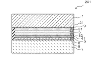
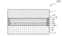
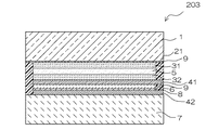
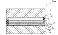
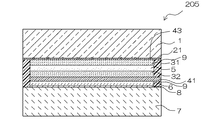
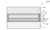
図1、図5、図6、図7、図8及び図9のように、本発明の色素増感型太陽電池201、202、203、204、205及び206は、第1基体101と、多孔質絶縁層6と、第2基体102と、を有する。
上記「第1基体101」は、透光性基板1、透光性基板1の表面に設けられた透光性導電層21、透光性導電層21の表面に設けられた増感色素311を有する第1半導体電極31(図3参照)、一面が第1半導体電極31と対向するように配置された増感色素321を有する第2半導体電極32(図4参照)、第2半導体電極32の他面に設けられた第1集電電極41、及び第1半導体電極31と第2半導体電極32との間に設けられた電解質層5を備える。この第1基体101の構成部材のうちで、第1集電電極41は多孔質絶縁層6及び第2基体102の側へと光を透過させる必要がないため、透光性を有していてもよく、透光性を有していなくてもよい。また、上記「第2基体102」は、基板7及び基板7の表面に設けられた触媒層8を備える。この第2基体102は、全体として透光性を有していてもよく、透光性を有していなくてもよい。従って、基板7及び触媒層8もそれぞれ透光性を有していてもよく、透光性を有していなくてもよい。
尚、この透光性とは、波長400〜900nmの可視光の透過率が10%以上であることを意味する。また、この透過率は60%以上、特に85%以上であることが好ましい。以下、透光性の意味及び好ましい透過率はすべて同様である。
透過率(%)=(透過した光量/入射した光量)×100
Hereinafter, the present invention will be described in detail.
As shown in FIGS. 1, 5, 6, 7, 8, and 9, the dye-sensitized
The “first substrate 101” includes the
In addition, this translucency means that the transmittance | permeability of visible light with a wavelength of 400-900 nm is 10% or more. The transmittance is preferably 60% or more, particularly 85% or more. Hereinafter, the meaning of translucency and preferable transmittance are all the same.
Transmittance (%) = (transmitted light amount / incident light amount) × 100
上記「透光性基板1」としては、ガラス、樹脂シート等からなる基板が挙げられる。樹脂シートは特に限定されず、ポリエチレンテレフタレート、ポリエチレンナフタレート等のポリエステル、ポリフェニレンスルフィド、ポリカーボネート、ポリスルフォン、ポリエチリデンノルボルネン等からなる樹脂シートが挙げられる。この透光性基板1の厚さは材質によっても異なり、特に限定されないが、上記の透過率が60〜99%、特に85〜99%となる厚さであることが好ましい。
Examples of the “
上記「透光性導電層21」は、透光性及び導電性を有しておればよい。この透光性導電層21は特に限定されず、導電性酸化物からなる薄膜、金属薄膜、炭素薄膜等が挙げられる。導電性酸化物としては、酸化スズ、フッ素ドープ酸化スズ(FTO)、酸化インジウム、スズドープ酸化インジウム(ITO)、酸化亜鉛等が挙げられる。また、金属としては、白金、金、銅、アルミニウム、ロジウム、インジウム等が挙げられる。この透光性導電層21の厚さは材質によっても異なり、特に限定されないが、表面抵抗が100Ω/cm2以下、特に1〜10Ω/cm2となる厚さであることが好ましい。更に、透光性導電層21の形成方法は特に限定されないが、金属、導電性酸化物等の微粒子を含有するペーストを、透光性基板1の表面に塗布して形成することができる。この塗布方法としては、ドクターブレード法、スキージ法、スピンコート法等の各種の方法が挙げられる。また、透光性導電層21は、金属、導電性酸化物等を用いたスパッタリング法、真空蒸着法、イオンプレーティング法等により形成することもできる。
The “translucent
上記「増感色素311」及び上記「増感色素321」としては、光電変換の作用を向上させる錯体色素及び有機色素を用いることができる。この錯体色素としては金属錯体色素が挙げられ、有機色素としてはポリメチン色素、メロシアニン色素等が挙げられる。金属錯体色素としてはルテニウム錯体色素及びオスミウム錯体色素等が挙げられ、ルテニウム錯体色素が特に好ましい。更に、光電変換がなされる波長域を拡大し、変換効率を向上させるため、増感作用が発現される波長域の異なる2種以上の増感色素を併用することもできる。この場合、照射される光の波長域と強度分布とによって併用する増感色素の種類及びそれらの量比を設定することが好ましい。また、増感色素は半導体電極に結合するための官能基を有することが好ましい。この官能基としては、カルボキシル基、スルホン酸基、シアノ基等が挙げられる。
As the “sensitizing
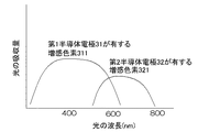
増感色素311及び増感色素321は同一のものであってもよい。即ち、第1半導体電極31及び第2半導体電極32の各々で吸収される光の波長域が同じであっても、半導体電極を2個設けることで、照射される光の利用効率を高くすることができ、光電変換効率が向上する。また、図2のように、増感色素311及び増感色素321の各々が吸収する光の波長域が異なる場合は、照射される光の利用効率をより高くすることができ、光電変換効率を更に向上させることができるため好ましい。吸収する光の波長域が異なる増感色素の組み合わせは特に限定されないが、吸収波長域が異なる範囲が広いほど光の利用効率がより高くなり、好ましい。
The sensitizing
更に、増感色素311及び増感色素321の各々が吸収する光の波長域が異なる場合、透光性基板1の側に設けられた第1半導体電極31が有する増感色素311が吸収する光の波長域が、第2半導体電極32が有する増感色素321が吸収する光の波長域より短波長側にあることが好ましい。このようにすれば、第1半導体電極31を透過し、第2半導体電極32に到達する光量を多くすることができ、光の利用効率をより向上させることができる。
Furthermore, when each of the sensitizing
また、増感色素311及び増感色素321のうちの少なくとも一方が、吸収する光の波長域の異なる2種以上の増感色素により構成されていることが好ましい。この場合、増感色素311及び増感色素321に含有されるすべての増感色素の各々が吸収する波長域がそれぞれ異なることがより好ましい。このようにすべての増感色素が吸収する光の波長域がそれぞれ異なっておれば、吸収することができる光の波長域をより広くすることができ、光の利用効率を特に大きく向上させることができる。
Moreover, it is preferable that at least one of the sensitizing
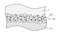
上記「第1半導体電極31」及び上記「第2半導体電極32」の各々の電極基体は、金属酸化物、金属硫化物等により形成することができる。金属酸化物としては、チタニア、酸化スズ、酸化亜鉛、五酸化二ニオブ等の酸化ニオブ、酸化タンタル、ジルコニア等が挙げられる。また、チタン酸ストロンチウム、チタン酸カルシウム、チタン酸バリウム等の複酸化物を用いることもできる。更に、金属硫化物としては、硫化亜鉛、硫化鉛、硫化ビスマス等が挙げられる。電極基体の作製方法は特に限定されず、例えば、金属酸化物、金属硫化物等の微粒子を含有するスラリーを、第1半導体電極31の場合は、第1基体101の透光性導電層21の表面に塗布し、焼成することにより作製することができる。また、第2半導体電極32の場合は、同様のスラリーを、多孔質絶縁層6及び第1集電電極41の表面、又は第1集電電極41の表面に塗布し、焼成することにより作製することができる。スラリーの塗布方法は特に限定されず、スクリーン印刷法、ドクターブレード法、スキージ法、スピンコート法等が挙げられる。このようにして作製された電極基体は微粒子が集合してなる集合体の形態で形成される。
The electrode bases of the “
電極基体は、第1半導体電極31の場合は、第1基体101の透光性導電層21の表面に、第2半導体電極32の場合は、多孔質絶縁層6及び第1集電電極41の表面、又は第1集電電極41の表面に、金属酸化物、金属硫化物等の微粒子及び少量の有機高分子等が分散されたコロイド溶液を塗布し、その後、乾燥し、次いで、加熱して有機高分子を分解させて除去することにより作製することもできる。このコロイド溶液も、スクリーン印刷法、ドクターブレード法、スキージ法、スピンコート法等の各種の方法により塗布することができる。この方法により作製した電極基体も微粒子が集合してなる集合体の形態で形成される。
In the case of the
このように、第1半導体電極31及び第2半導体電極32の各々の電極基体は、通常、微粒子が集合してなる集合体の形態で形成される。この微粒子のX線回折により測定した平均粒径は特に限定されないが、5〜100nm、特に10〜40nmであることが好ましい。更に、第1半導体電極31の電極基体の平均粒径が、第2半導体電極32の電極基体の平均粒径より小さいことがより好ましい。これにより、受光面側である第1半導体電極31を透過する光量を多くすることができ、光の利用効率を更に向上させることができる。この第1半導体電極31の電極基体の平均粒径と、第2半導体電極32の電極基体の平均粒径との差は特に限定されないが、5〜60nm、特に10〜50nmであることが好ましい。また、第1半導体電極31の電極基体の平均粒径が10〜20μmであり、第2半導体電極32の電極基体の平均粒径が30〜50μmであれば、第1半導体電極31を透過し、第2半導体電極32に到達する光量を十分に多くすることができ、光の利用効率をより向上させることができる。
As described above, the electrode bases of the
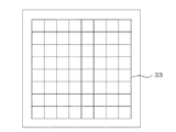
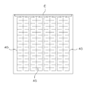
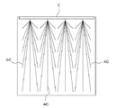
第1半導体電極31及び第2半導体電極32の各々の形状は特に限定されず、平面状、又は線状の電極からなり且つ特定の電極パターンにより形成されている電極とすることができる。第1半導体電極31は、通常、平面状であり、透光性導電層21の表面のうちの接合部が形成される周縁部を除く部分に設けられる。一方、第2半導体電極32は線状の電極からなり且つ特定のパターンにより形成されている電極とすることが好ましい。この特定のパターンは特に限定されず、例えば、図10のような格子状33、図11のような櫛歯状34、図12のような放射状35等とすることができる。線状の電極からなり且つ特定のパターンにより形成されている第2半導体電極32の場合、線状の電極の幅及び厚さは特に限定されず、その光電変換効率及びコスト等を勘案し設定することが好ましい。このように、第2半導体電極32を線状の電極からなり且つ特定のパターンにより形成されている電極とすることにより、電解質等を触媒層に向けて容易に移動させることができる。
Each shape of the
更に、第1半導体電極31及び第2半導体電極32のそれぞれが特に平面状である場合、それらの各々の厚さは特に限定されないが、0.1〜100μmとすることができ、1〜50μm、特に2〜40μm、更に5〜30μmとすることが好ましい。各々の半導体電極の厚さが0.1〜100μmであれば、光電変換が十分になされ、光電変換効率が向上する。また、第1半導体電極31は0.1〜25μm、特に0.5〜20μm、更に1〜15μmとし、第2半導体電極32は5〜100μm、特に10〜50μm、更に15〜30μmとし、且つ第1半導体電極31を第2半導体電極32より薄層とすることが好ましい。このように各々の電極の厚さを調整することによって、第1半導体電極31を透過し、第2半導体電極32に到達する光量を十分に多くすることができ、光の利用効率をより向上させることができる。
尚、第1半導体電極31は、その強度及び透光性導電層21との密着性を向上させるため、第2半導体電極32は、その強度並びに多孔質絶縁層6及び第1集電電極41との密着性を向上させるため、熱処理することが好ましい。熱処理の温度及び時間は特に限定されないが、熱処理温度は40〜700℃、特に100〜500℃、熱処理時間は10分〜10時間、特に20分〜5時間とすることが好ましい。尚、第1半導体電極31の側では、透光性基板1として樹脂シートを用いるときは、樹脂が熱劣化しないように低温で熱処理することが好ましい。
Furthermore, when each of the
Since the
電極基体に増感色素を付着させる方法は特に限定されず、例えば、増感色素を有機溶媒に溶解させた溶液に電極基体を浸漬し、溶液を含浸させ、その後、有機溶媒を除去することにより付着させることができる。また、この溶液を、電極基体に塗布し、その後、有機溶媒を除去することにより付着させることもできる。この塗布方法としては、ワイヤーバー法、スライドホッパー法、エクストルージョン法、カーテンコート法、スピンコート法、スプレーコート法等が挙げられる。更に、この溶液は、オフセット印刷、グラビア印刷、スクリーン印刷等の印刷法により塗布することもできる。 The method for attaching the sensitizing dye to the electrode substrate is not particularly limited. For example, the electrode substrate is immersed in a solution in which the sensitizing dye is dissolved in an organic solvent, impregnated with the solution, and then the organic solvent is removed. Can be attached. Alternatively, this solution can be applied to the electrode substrate and then adhered by removing the organic solvent. Examples of the coating method include a wire bar method, a slide hopper method, an extrusion method, a curtain coating method, a spin coating method, and a spray coating method. Furthermore, this solution can also be applied by a printing method such as offset printing, gravure printing or screen printing.
増感色素の付着量は半導体電極1gに対して0.01〜1ミリモル、特に0.5〜1ミリモルであることが好ましい。付着量が0.01〜1ミリモルであれば、半導体電極における光電変換が効率よくなされる。また、増感色素は電極基体の少なくとも表面に付着しておればよいが、電極基体の表面から90%の距離の内部にまで付着、含有されることが好ましく、通常、電極基体の全体に付着、含有される。これにより光電変換効率をより向上させることができる。尚、電極基体に付着しなかった増感色素が電極周辺に遊離していると、変換効率が低下することがある。そのため、増感色素を付着させる処理の後、半導体電極を洗浄して余剰の増感色素を除去することが好ましい。この除去は、洗浄槽を用いてアセトニトリル等の極性溶媒及びアルコール系溶媒などの有機溶媒で洗浄することにより行うことができる。また、電極基体に多くの増感色素を付着させるためには、電極基体を加熱して、浸漬、塗布等の処理を行うことが好ましい。この場合、電極基体の表面に水が吸着するのを避けるため、加熱後、常温に降温させることなく40〜80℃で速やかに処理することが好ましい。 The adhesion amount of the sensitizing dye is preferably 0.01 to 1 mmol, particularly 0.5 to 1 mmol with respect to 1 g of the semiconductor electrode. When the adhesion amount is 0.01 to 1 mmol, photoelectric conversion in the semiconductor electrode is efficiently performed. Further, the sensitizing dye may be attached to at least the surface of the electrode substrate, but is preferably attached and contained within a distance of 90% from the surface of the electrode substrate, and is usually attached to the entire electrode substrate. Contained. Thereby, a photoelectric conversion efficiency can be improved more. If the sensitizing dye that has not adhered to the electrode substrate is liberated around the electrode, the conversion efficiency may decrease. For this reason, it is preferable to remove the excess sensitizing dye by washing the semiconductor electrode after the treatment for attaching the sensitizing dye. This removal can be performed by washing with a polar solvent such as acetonitrile and an organic solvent such as an alcohol solvent using a washing tank. Moreover, in order to attach many sensitizing dyes to the electrode substrate, it is preferable to heat the electrode substrate and perform a treatment such as dipping or coating. In this case, in order to avoid water adsorbing on the surface of the electrode substrate, it is preferable to perform the treatment promptly at 40 to 80 ° C. without heating to room temperature after heating.
上記「第1集電電極41」は、第2半導体電極32の他面に設けられる。この第1集電電極41の形状は特に限定されず、図1のように平面状とすることができる。但し、第2半導体電極32と触媒層8との間には電解質を介在させなければならないため、平面状である場合、特に、第1集電電極41の面積が、第2半導体電極32の面積の10%以上、特に30%以上であるときは多孔質体であることが好ましい。更に、第1集電電極41が第2半導体電極32の他面の全面に接して形成されたときは、第1集電電極41を、電解質が含有され、且つ移動することができる多孔質体とする必要がある。この多孔質体の断面を電子顕微鏡により観察し、視野の全面積に対する空孔部分の面積の面積比として算出した空孔率は特に限定されないが、2〜40%、特に10〜30%、更に15〜25%とすることができる。空孔率が2〜40%、特に10〜30%であれば、第1集電電極41に所要量の電解質を含有させることができ、且つ電解質を十分に移動させることができる。この多孔質体からなる第1集電電極41は、タングステン、チタン、ニッケル等の金属成分と、アルミナ等の酸化物造孔剤などとを含有するメタライズインクを用いて形成した塗膜を焼成し、作製することができる。
The “first current collecting
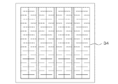
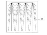
第1集電電極41は、図5のように、線状の電極からなり且つ特定の電極パターンにより形成されている電極とすることもできる。この特定のパターンは特に限定されず、例えば、図13のような格子状44、図14のような櫛歯状45、図15のような放射状46等の集電電極とすることができる。また、この線状の電極からなり且つ特定の電極パターンにより形成されている第1集電電極41の場合、線状の電極の幅及び厚さは特に限定されず、その電気抵抗及びコスト等を勘案し設定することが好ましい。更に、第1集電電極41が格子状、櫛歯状又は放射状等の特定のパターンで配設される場合、第1集電電極41の全面積は、第2半導体電極32の全面積に対して1〜90%、特に5〜50%、更に10〜20%であることが好ましい。第1集電電極41の全面積が、第2半導体電極32の全面積に対して1〜90%、特に5〜50%であれば、第1集電電極41が配設されていない部分に十分に電解質を介在させることができ、且つ電解質を容易に移動させることができる。
As shown in FIG. 5, the first current collecting
上記「電解質層5」は、電解質溶液により形成することができる。この電解質溶液には、電解質の他、通常、溶媒及び各種の添加剤等が含有される。電解質としては、(1)I2とヨウ化物、(2)Br2と臭化物、(3)フェロシアン酸塩−フェリシアン酸塩、フェロセン−フェリシニウムイオン等の金属錯体、(4)ポリ硫化ナトリウム、アルキルチオール−アルキルジスルフィド等のイオウ化合物、(5)ビオロゲン色素、(6)ヒドロキノン−キノン、などを含有する電解質が挙げられる。(1)におけるヨウ化物としては、LiI、NaI、KI、CsI、CaI2等の金属ヨウ化物、及びテトラアルキルアンモニウムヨーダイド、ピリジニウムヨーダイド、イミダゾリウムヨーダイド等の4級アンモニウム化合物のヨウ素塩などが挙げられる。また、(2)における臭化物としては、LiBr、NaBr、KBr、CsBr、CaBr2等の金属臭化物、及びテトラアルキルアンモニウムブロマイド、ピリジニウムブロマイド等の4級アンモニウム化合物の臭素塩などが挙げられる。これらの電解質のうちでは、I2と、LiI及びピリジニウムヨーダイド、イミダゾリウムヨーダイド等の4級アンモニウム化合物のヨウ素塩とを組み合わせてなる電解質が特に好ましい。これらの電解質は1種のみを用いてもよいし、2種以上を用いてもよい。
The “
電解質層5に含有される溶媒は、粘度が低く、イオン易動度が高く、十分なイオン伝導性を有する溶媒であることが好ましい。このような溶媒としては、(1)エチレンカーボネート、プロピレンカーボネート等のカーボネート類、(2)3−メチル−2−オキサゾリジノン等の複素環化合物、(3)ジオキサン、ジエチルエーテル等のエーテル類、(4)エチレングリコールジアルキルエーテル、プロピレングリコールジアルキルエーテル、ポリエチレングリコールジアルキルエーテル、ポリプロピレングリコールジアルキルエーテル等の鎖状エーテル類、(5)メタノール、エタノール、エチレングリコールモノアルキルエーテル、プロピレングリコールモノアルキルエーテル、ポリエチレングリコールモノアルキルエーテル、ポリプロピレングリコールモノアルキルエーテル等のモノアルコール類、(6)エチレングリコール、プロピレングリコール、ポリエチレングリコール、ポリプロピレングリコール、グリセリン等の多価アルコール類、(7)アセトニトリル、グルタロジニトリル、メトキシアセトニトリル、プロピオニトリル、ベンゾニトリル等のニトリル類、(8)ジメチルスルフォキシド、スルフォラン等の非プロトン極性物質などが挙げられる。
The solvent contained in the
この電解質層5の厚さは特に限定されないが、100μm以下、特に20μm以下とすることができ、この厚さが100μm以下、特に20μm以下であれば、光電変換効率を十分に高くすることができる。更に、第1半導体電極31と第2半導体電極32とを接触させることができ、この場合、形成される空隙の厚さが20μm以下(通常、1μm以上である。)であれば、光電変換効率を十分に高くすることができる。
The thickness of the
電解質層5は、第1半導体電極31と第2半導体電極32との間に設けられる。この電解質層5を設ける方法は特に限定されないが、例えば、透光性基板1と基板7との間、又は透光性導電層21と基板7との間、基板7の側に透光性導電層21の場合と同様にして導電層22が設けられるときは、透光性基板1と基板7との間、透光性導電層21と基板7との間、透光性基板1と導電層22との間、又は透光性導電層21と導電層22との間を、第1半導体電極31及び第2半導体電極32等の周囲において樹脂又はガラスにより封着し、形成される密閉空間に電解質溶液を注入し、設けることができる。この密閉空間への電解質溶液の注入は、透光性基板1の側からでも、基板7の側からでもよいが、穿孔する必要がある部材の少ない透光性基板1の側に注入口を設けることが好ましい。尚、注入口は1個でよいが、空気抜きのため更に他の孔を設けることもできる。このように空気抜きのための孔を設けることで、電解質溶液をより容易に注入することができる。
The
第1半導体電極31及び第2半導体電極32等の周囲の封着に用いられる樹脂としては、エポキシ樹脂、ウレタン樹脂、ポリイミド樹脂、熱硬化性ポリエステル樹脂等の熱硬化性樹脂が挙げられる。更に、この封着はガラスにより行うこともでき、特に長期の耐久性を必要とする太陽電池では、ガラスにより封着することが好ましい。
Examples of the resin used for sealing around the
電解質層5は、不揮発性のイミダゾリウム塩等のイオン性液体及びこのイオン性液体をゲル化させたもの、並びにヨウ化銅、チオシアン化銅等の固体により設けることもできる。また、この電解質層5の厚さは特に限定されないが、電解質溶液を用いた場合と同様に、100μm以下、特に20μm以下(通常、1μm以上である。)とすることができる。各々の場合の厚さの上限が所定値以下であれば、変換効率を十分に高くすることができる。
The
第2半導体電極32及び第1集電電極41、又は第1集電電極41と接して設けられる上記「多孔質絶縁層6」の材質は特に限定されないが、セラミックにより形成することが好ましい。このセラミックは特に限定されず、酸化物系セラミック、窒化物系セラミック、炭化物系セラミック等の各種のセラミックを用いることができる。酸化物系セラミックとしては、アルミナ、ムライト、ジルコニア等が挙げられる。また、窒化物系セラミックとしては、窒化ケイ素、サイアロン、窒化チタン、窒化アルミニウム等が挙げられる。更に、炭化物系セラミックとしては、炭化ケイ素、炭化チタン、炭化アルミニウム等が挙げられる。セラミックとしては、アルミナ、窒化ケイ素、ジルコニア等が好ましく、アルミナが特に好ましい。
The material of the “porous insulating
多孔質絶縁層6の空孔率は特に限定されないが、この多孔質絶縁層6の断面を電子顕微鏡により観察し、視野の全面積に対する空孔部分の面積の面積比として算出した空孔率が、2〜40%、特に10〜30%、更に15〜25%であることが好ましい。この空孔率が2〜40%、特に10〜30%であれば、電解質の含有、移動が容易であり、光電変換の作用が損なわれることがない。また、この多孔質絶縁層6の厚さも特に限定されないが、0.5〜20μm、特に1〜10μm、更に2〜7μmとすることができる。この多孔質絶縁層6の厚さが0.5μm以上であれば、半導体電極側と触媒層側とを電気的に絶縁することができる。
The porosity of the porous insulating
多孔質絶縁層6は、マグネトロンスパッタ法、電子ビ−ム蒸着法等の物理的蒸着法などで、アルミナ、窒化ケイ素、ジルコニア等のセラミックを触媒層8の表面に堆積させて設けることができる。更に、各々のセラミック成分、焼結助剤及び有機バインダ等を含有するスラリーを用いて、スクリーン印刷法等により触媒層8の表面に塗膜を形成し、その後、多孔質体とすることができる条件で焼成する方法により形成することができる。また、各々のセラミック成分、焼結助剤、有機バインダ及びカーボン等の造孔剤などを含有するペーストを用いて、スクリーン印刷法等により触媒層8の表面に塗膜を形成し、その後、所定温度で所要時間焼成する方法等により形成することができる。
The porous
上記「基板7」は、透光性を有していてもよく、透光性を有していなくてもよい。透光性を有する基板7は、透光性基板1の場合と同様にガラス、樹脂シート等を用いて設けることができる。樹脂シートである場合、このシートの形成に用いる樹脂としては、ポリエステル、ポリフェニレンスルフィド、ポリカーボネート、ポリスルフォン、ポリエチリデンノルボルネン等の熱可塑性樹脂などが挙げられる。この基板7が透光性を有する基板である場合、その厚さは材質によっても異なり、特に限定されないが、前記の透過率が60〜99%、特に85〜99%となる厚さであることが好ましい。
The “
透光性を有していない基板7はセラミックにより形成することができる。セラミック基板は強度が大きく、この基板が支持基板となって優れた耐久性を有する色素増感型太陽電池とすることができる。セラミック基板の形成に用いるセラミックは特に限定されず、酸化物系セラミック、窒化物系セラミック、炭化物系セラミック等の各種のセラミックを用いることができる。酸化物系セラミックとしては、アルミナ、ムライト、ジルコニア等が挙げられる。また、窒化物系セラミックとしては、窒化ケイ素、サイアロン、窒化チタン、窒化アルミニウム等が挙げられる。更に、炭化物系セラミックとしては、炭化ケイ素、炭化チタン、炭化アルミニウム等が挙げられる。セラミックとしては、アルミナ、窒化ケイ素、ジルコニア等が好ましく、アルミナが特に好ましい。
The
基板7がセラミックからなる場合、その厚さは特に限定されないが、100μm〜5mm、特に500μm〜5mm、更に800μm〜5mmとすることができ、500μm〜2mmとすることもできる。セラミック基板の厚さが100μm〜5mm、特に800μm〜5mmであれば、この強度の大きい基板が支持基板となり、優れた耐久性を有する色素増感型太陽電池とすることができる。
When the board |
上記「触媒層8」は、触媒活性を有する物質、又は触媒活性を有する物質を含有する、金属、前記の透光性導電層の形成に用いられる導電性酸化物及び導電性高分子のうちの少なくとも1種、により形成することができる。触媒活性を有する物質としては、白金、金、ロジウム等の貴金属(但し、銀は電解質等に対する耐腐食性が低いため好ましくない。以下、電解質等が接触し得る部分には同様に銀は好ましくない。)、カーボンブラック等が挙げられ、これらは併せて導電性を有する。触媒層は、触媒活性を有し、且つ電気化学的に安定な貴金属により形成することが好ましく、触媒活性が高く、電解質溶液に溶解され難い白金を用いることが特に好ましい。 The “catalyst layer 8” includes a substance having a catalytic activity or a substance having a catalytic activity, of a metal, a conductive oxide and a conductive polymer used for forming the light-transmitting conductive layer. At least one kind can be formed. As a substance having catalytic activity, noble metals such as platinum, gold and rhodium (however, silver is not preferred because of its low corrosion resistance to electrolytes, etc. Hereinafter, silver is also not preferred for the parts where the electrolyte etc. can contact) .), Carbon black and the like, and these have conductivity together. The catalyst layer is preferably formed of a noble metal having catalytic activity and electrochemically stable, and it is particularly preferable to use platinum that has high catalytic activity and is hardly dissolved in the electrolyte solution.
触媒活性を有さない、金属、導電性酸化物及び導電性高分子等を用いる場合、触媒層に混合されて用いられる金属としては、アルミニウム、銅、クロム、ニッケル、タングステン等が挙げられる。更に、触媒層に混合されて用いられる導電性高分子としては、ポリアニリン、ポリピロール、ポリアセチレン等が挙げられる。また、この導電性高分子としては、導電性を有さない樹脂に各種の導電性物質を配合して調製したものが挙げられる。この樹脂は特に限定されず、熱可塑性樹脂でも熱硬化性樹脂でもよい。熱可塑性樹脂としては、熱可塑性ポリエステル樹脂、ポリアミド、ポリオレフィン、ポリ塩化ビニル等が挙げられる。更に、熱硬化性樹脂としては、エポキシ樹脂、熱硬化性ポリエステル樹脂、フェノール樹脂等が挙げられる。導電性物質も特に限定されず、カーボンブラック、白金、金、ロジウム等の貴金属及び銅、アルミニウム、ニッケル、クロム、タングステンなどの金属、ポリアニリン、ポリピロール、ポリアセチレン等の導電性ポリマーなどが挙げられる。導電性物質としては、導電性と触媒活性とを併せて有するカーボンブラック及び貴金属が特に好ましい。導電性物質は1種のみを用いてもよく、2種以上を用いてもよい。
触媒活性を有さない、金属、導電性酸化物及び導電性高分子等を用いる場合、上記の触媒活性を有する物質の含有量は、金属、導電性酸化物、導電性高分子等を100質量部とした場合に、1〜99質量部、特に50〜99質量部であることが好ましい。
In the case of using a metal, a conductive oxide, a conductive polymer, or the like that does not have catalytic activity, examples of the metal used by mixing with the catalyst layer include aluminum, copper, chromium, nickel, tungsten, and the like. Furthermore, polyaniline, polypyrrole, polyacetylene, etc. are mentioned as a conductive polymer used by mixing with a catalyst layer. Moreover, as this conductive polymer, what was prepared by mix | blending various electroconductive substances with resin which does not have electroconductivity is mentioned. This resin is not particularly limited, and may be a thermoplastic resin or a thermosetting resin. Examples of the thermoplastic resin include thermoplastic polyester resin, polyamide, polyolefin, polyvinyl chloride, and the like. Furthermore, examples of the thermosetting resin include an epoxy resin, a thermosetting polyester resin, and a phenol resin. The conductive material is not particularly limited, and examples thereof include noble metals such as carbon black, platinum, gold and rhodium, metals such as copper, aluminum, nickel, chromium and tungsten, and conductive polymers such as polyaniline, polypyrrole and polyacetylene. As the conductive material, carbon black and noble metal having both conductivity and catalytic activity are particularly preferable. Only one type of conductive material may be used, or two or more types may be used.
When metals, conductive oxides, conductive polymers, etc. that do not have catalytic activity are used, the content of the above-mentioned substances having catalytic activity is 100 masses of metals, conductive oxides, conductive polymers, etc. Parts, preferably 1 to 99 parts by mass, particularly 50 to 99 parts by mass.
このように、触媒層8は、導電性及び触媒活性を有する物質により形成することができる。また、触媒活性を有する物質を含有する、金属、導電性酸化物及び導電性高分子のうちの少なくとも1種により形成することもできる。更に、触媒層は、1種の材料のみからなる層でもよく、2種以上の材料からなる混合層でもよい。また、触媒層は、単層でもよく、金属層、導電性酸化物層、導電性高分子層、並びに金属、導電性酸化物及び導電性高分子のうちの2種以上からなる混合層のうちの2層以上からなる多層の触媒層でもよい。この触媒層の厚さは特に限定されないが、単層及び多層のいずれの場合も、3nm〜10μm、特に3nm〜2μmとすることができる。触媒層の厚さが3nm〜10μmであれば、十分に抵抗の低い触媒層とすることができる。 Thus, the catalyst layer 8 can be formed of a substance having conductivity and catalytic activity. Further, it can be formed of at least one of a metal, a conductive oxide and a conductive polymer containing a substance having catalytic activity. Furthermore, the catalyst layer may be a layer made of only one material or a mixed layer made of two or more materials. In addition, the catalyst layer may be a single layer, of a metal layer, a conductive oxide layer, a conductive polymer layer, and a mixed layer composed of two or more of a metal, a conductive oxide, and a conductive polymer. A multilayer catalyst layer composed of two or more layers may be used. Although the thickness of this catalyst layer is not particularly limited, it can be 3 nm to 10 μm, particularly 3 nm to 2 μm in both cases of a single layer and multiple layers. When the thickness of the catalyst layer is 3 nm to 10 μm, a sufficiently low resistance catalyst layer can be obtained.
触媒活性を有する物質からなる触媒層8は、触媒活性を有する物質の微粒子を含有するメタライズインクを、基板7の表面、又は後記のように導電層22を有する場合は、この導電層22の表面に塗布して形成することができる。また、触媒活性を有する物質を含有する金属、導電性酸化物からなる触媒層8も、触媒活性を有する物質の場合と同様の方法により形成することができる。この塗布方法としては、スクリーン印刷法、ドクターブレード法、スキージ法、スピンコート法等の各種の方法が挙げられる。更に、この触媒層8は、スパッタリング法、蒸着法、イオンプレーティング法等により、基板7等の表面に金属等を堆積させて形成することもできる。また、触媒活性を有する物質を含有する導電性高分子からなる触媒層8は、導電性高分子と、粉末状又は繊維状等の触媒活性を有する物質とを、バンバリーミキサ、インターナルミキサー、オープンロール等の装置により混練して調製した樹脂組成物をフィルムに成形し、このフィルムを基板7等の表面に接合して形成することができる。更に、樹脂組成物を溶媒に溶解又は分散させて調製した溶液又は分散液を基板7等の表面に塗布し、乾燥して、溶媒を除去し、必要に応じて加熱して形成することもできる。尚、触媒層8が混合層であるときは、含有される材料の種類に応じて、上記の各種の方法等のうちの適宜の方法により形成することができる。
The catalyst layer 8 made of a substance having a catalytic activity is formed by using a metallized ink containing fine particles of a substance having a catalytic activity on the surface of the
基板7と触媒層8との間、又は後記のように基板7と触媒層8との間に導電層22が設けられる場合は、基板7と導電層22との間若しくは導電層22の表面に第2集電電極42を設けることもできる。この第2集電電極42は、触媒層8を白金、金等の導電性に優れる貴金属により形成し、特に20nm以上、更に1μm以上(通常、10μm以下)と厚くした場合は、導電性の観点からは設ける必要はないが、コストの面では設けることが好ましい。即ち、白金等は高価であるため、触媒層8をできるだけ薄層とすることが好ましいが、薄層であると抵抗が高くなるため、タングステン、チタン、ニッケル等の金属からなる第2集電電極42を設けることで、集電効率を向上させるとともに、コストを低減することができる。更に、触媒層8を前記の導電性酸化物に触媒活性を有する物質を配合した組成物等により形成したときは、触媒層8の抵抗はより高くなるため、第2集電電極42を設け、集電効率を高めることがより好ましい。
When the
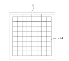
第2集電電極42の形状も特に限定されないが、第2基体102の側では透光性は必須でないため、図6のように、第2集電電極42を平面状とすることができる。この第2集電電極42は電解質を移動させる必要はないため、平面状である場合、多孔質体でなくてもよいが、多孔質体であってもよい。また、抵抗の低い第2集電電極42とするためには、触媒層8と類似の平面形状であり、且つ触媒層8に対して50%以上、特に65%以上、更に80%以上(同面積でもよい。)の面積の平面状の電極であることが好ましい。更に、触媒層8と相似形に配設されることがより好ましい。また、第2集電電極42は、図7のように、線状の電極からなり且つ特定の電極パターンにより形成されている電極とすることもできる。この特定のパターンは特に限定されず、例えば、図13のような格子状44、図14のような櫛歯状45、図15のような放射状46等とすることができる。この線状の電極からなり且つ特定の電極パターンにより形成されている第2集電電極42の場合、線状の電極の幅及び厚さは特に限定されず、その電気抵抗及びコスト等を勘案し設定することが好ましい。第2集電電極42が線状の電極からなり且つ特定の電極パターンにより形成されている電極である場合、第2集電電極42の全面積は特に限定されないが、触媒層8の全面積に対して0.1%以上、特に5%以上、更に10%以上とすることができる。また、この全面積は90%以上とすることもでき、このように面積の広い第2集電電極42であれば、集電効率をより高めることができる。
The shape of the second current collecting
更に、透光性基板1と透光性導電層21との間、又は透光性導電層21の表面に更に第3集電電極43を設けることもできる。この第3集電電極43の形状は透光性が保持される限り特に限定されず、線状の電極からなり且つ特定の電極パターンにより形成されている電極とすることができる。例えば、図13のような格子状44、図14のような櫛歯状45、図15のような放射状46等の形状の電極とすることができる。また、この線状の電極からなり且つ特定の電極パターンにより形成されている第3集電電極43の場合、線状の電極の幅及び厚さは特に限定されず、その電気抵抗及びコスト等を勘案し設定することが好ましい。第3集電電極43の全面積は、第1半導体電極31の全面積に対して0.1〜20%、特に0.1〜5%、更に0.1〜1%であることが好ましい。第3集電電極43の全面積が第1半導体電極31の全面積に対して0.1〜20%であれば、集電効率を高めることができ、且つ第1半導体電極31に照射される光量を十分に保持することができる。
Further, a third current collecting
第1集電電極41、第2集電電極42及び第3集電電極43を設ける方法は特に限定されないが、例えば、所定のパターンが形成されたマスクを用いて、マグネトロンスパッタ法及び電子ビ−ム蒸着法等の物理的蒸着法などでタングステン、チタン、ニッケル等の金属を堆積させ、その後、フォトリソグラフィー等によりパターニングする方法が挙げられる。また、各々の金属成分を含有するメタライズインクを用いてスクリーン印刷法等によりパターニングし、その後、焼成する方法などにより形成することができる。物理的蒸着法などに用いる金属としては、タングステン、チタン、ニッケルの他、白金、金等の貴金属、銅等を用いることもできる。この金属としては、耐腐食性に優れるタングステン、チタン、ニッケル、貴金属等を用いることが好ましい。更に、メタライズインクに含有される金属としても、タングステン、チタン、ニッケル、白金、金等の貴金属、銅等を用いることができる。この金属としては、耐腐食性に優れるタングステン、チタン、ニッケル、貴金属等を用いることが好ましい。尚、これらの方法において、物理的蒸着及び焼成の条件により、集電電極の緻密度を調整することができ、特に、第1集電電極41の場合、前記の空孔率を有する多孔質体からなる集電電極とすることもできる。
The method for providing the first current collecting
本発明の色素増感型太陽電池の作製方法は特に限定されないが、例えば、以下の方法により作製することができる。
透光性基板1、透光性導電層21及び第1半導体電極31をこの順に積層してなる積層体、又は第3集電電極43を設ける場合は、透光性基板1と透光性導電層21との間若しくは透光性導電層21の表面に更に第3集電電極43を積層してなる積層体と、基板7、触媒層8、多孔質絶縁層6、第1集電電極41及び第2半導体電極32をこの順に積層してなる積層体、又は第2集電電極42を設ける場合は、基板7と触媒層8との間に更に第2集電電極42を積層してなる積層体とを、第1半導体電極31と第2半導体電極32とを対向させて積層し、色素増感型太陽電池とすることができる。
Although the manufacturing method of the dye-sensitized solar cell of this invention is not specifically limited, For example, it can manufacture with the following method.
When the
以下、実施例により本発明を具体的に説明する。
以下のようにして図8に示す色素増感型太陽電池205を作製した。
実施例1
(1)一方の積層体の作製
縦100mm、横100mm、厚さが1mmのガラス基板1の表面に、タングステンを用いて、RFスパッタリングにより、幅1mm、間隔10mm、厚さ1μmの格子状の第3集電電極43を形成した。その後、この第3集電電極43が形成されたガラス基板1の表面に、RFスパッタリングにより、厚さ500nmのフッ素ドープ酸化スズからなる透光性導電層21を形成した。次いで、この透光性導電層21の表面に、粒径が10〜20nmのチタニア粒子を含有するスラリー(Solaronix社製、商品名「Ti−Nonoxide D/SP」)をスクリーン印刷法により塗布し、120℃で1時間乾燥し、その後、480℃で30分焼成して、縦90mm、横90mm、厚さ20μmのチタニア電極層(電極基体)を形成した。次いで、この積層体を、ルテニウム錯体(Solaronix社製、商品名「535bis−TBA」)のエタノール溶液に10時間浸漬して、図3に一部を拡大して示すように、チタニア焼結粒子に400〜600nmの波長域の光を吸収する増感色素311であるルテニウム錯体を付着させて第1半導体電極31を形成し、一方の積層体を作製した。
Hereinafter, the present invention will be described specifically by way of examples.
The dye-sensitized
Example 1
(1) Fabrication of one laminated body A grid-shaped first substrate having a width of 1 mm, an interval of 10 mm, and a thickness of 1 μm is formed by RF sputtering using tungsten on the surface of a
(2)他方の積層体の作製
純度99.9質量%のアルミナ粉末100質量部に、焼結助剤として5質量部のマグネシア、カルシア及びシリカの混合粉末及び2質量部のバインダ並びに溶媒を配合してスラリーを調製し、このスラリーを用いてドクターブレード法により厚さ2mmのアルミナグリーンシートを作製した。その後、白金成分を含有するメタライズインクを用いてアルミナグリーンシートの表面にスクリーン印刷法により触媒層8となる厚さ500nmの導電塗膜を形成した。次いで、この導電塗膜の表面に、上記スラリーに更に造孔剤としてカーボンが配合されたスラリーを用いて多孔質絶縁層6となる厚さ μmの絶縁塗膜を形成した。その後、この絶縁塗膜の表面に、上記メタライズインクに更に造孔剤としてアルミナ粉末が配合されたインクを用いて第1集電電極41となる厚さ5μmの導電塗膜を形成した。次いで、還元雰囲気にて1500℃で一体焼成し、厚さ1mmのアルミナ基板7の表面に、縦90mm、横90mm、厚さ500nmの触媒層8、縦90mm、横90mm、厚さ5μmの多孔質絶縁層6、及び縦90mm、横90mm、厚さ5μmの第1集電電極41(但し、電流取り出しのための端子部は除く。)をこの順に形成した。その後、この第1集電電極41の表面に上記のチタニア粒子を含有するスラリーをスクリーン印刷法により塗布し、同様にして乾燥し、焼成して、縦90mm、横90mm、厚さ20μmのチタニア電極層(電極基体)を形成した。次いで、この積層体を、500〜700nmの波長域の光を吸収する有機色素である増感色素321を含有する溶液に10時間浸漬して、チタニア焼結粒子に増感色素321を付着させて第2半導体電極32を形成し、他方の積層体を作製した。
(2) Production of the other laminate A mixture of 5 parts by mass of magnesia, calcia, and silica, 2 parts by mass of binder and solvent as a sintering aid was added to 100 parts by mass of alumina powder with a purity of 99.9% by mass. Then, a slurry was prepared, and an alumina green sheet having a thickness of 2 mm was produced using this slurry by a doctor blade method. Thereafter, a conductive coating film having a thickness of 500 nm to be the catalyst layer 8 was formed on the surface of the alumina green sheet by a screen printing method using a metallized ink containing a platinum component. Next, an insulating coating film having a thickness of μm to be the porous insulating
(3)色素増感型太陽電池の作製
他方の積層体のアルミナ基板7の触媒層8が形成されていない部分に、熱可塑性樹脂からなる厚さ60μmの接着剤シート(Solaronix社製、商品名「SX1170−60」)を配設し、その後、一方の積層体を、その第1半導体電極31と他方の積層体の第2半導体電極32とが対向するように配置し、次いで、アルミナ基板7の側を下にして100℃に調温されたホットプレートに載せ、5分加熱して一方の積層体の透光性導電層21と他方の積層体のアルミナ基板7とを接合し、接合部9を形成した。その後、一方の積層体の所定の位置に設けられた電解質溶液の注入口からヨウ素電解液(Solaronix社製、商品名「Iodolyte PN−50」)を注入し、第1半導体電極31と第2半導体電極32と間に電解質層5を形成した。尚、注入したヨウ素電解液は多孔質の第1集電電極41及び多孔質絶縁層6に含有され、更に移動して触媒層8の表面に到達する。このようにして色素増感型太陽電池201を作製した。ヨウ素電解液注入後、注入口は上記の接着剤を用いて封止した。尚、電力は第3集電電極43及び第1集電電極41並びに触媒層8の各々から取り出した。
(3) Production of dye-sensitized solar cell An adhesive sheet (made by Solaronix, trade name) made of a thermoplastic resin on a portion of the other laminate on which the
(4)色素増感型太陽電池の性能評価
上記(1)〜(3)により作製した色素増感型太陽電池205に、AM1.5にスペクトル調整したソーラーシミュレータによって、照射強度100mW/cm2の擬似太陽光を照射したところ、変換効率10.5%の特性を有していた。
(4) Performance evaluation of dye-sensitized solar cell The dye-sensitized
実施例2
図9のように、セラミック基板7の表面に、スパッタリング法によりタングステンからなる厚さ1μmの平面状の第2集電電極42を設け、この第2集電電極42の表面に触媒層8を設けた他は実施例1と同様にして色素増感型太陽電池206を作製した。尚、電力は第3集電電極43及び第1集電電極41並びに第2集電電極42の各々から取り出した。その性能を実施例1の場合と同様にして評価したところ、変換効率10.8%の特性であり、実施例1と比べて優れており、触媒層の側にも集電電極を設けることで、光電変換効率がより向上することが分かる。
Example 2
As shown in FIG. 9, a planar second current collecting
比較例1
第1集電電極41を設けなかった他は実施例1と同様にして色素増感型太陽電池を作製し、その性能を実施例1の場合と同様にして評価したところ、変換効率6.2%の特性であり、実施例1及び実施例2と比べて特性が劣っていることが分かる。
Comparative Example 1
A dye-sensitized solar cell was produced in the same manner as in Example 1 except that the first current collecting
尚、本発明では、上記の実施例の記載に限られず、本発明の範囲内で種々変更した実施例とすることができる。例えば、第2基体102は、基板7と触媒層8との間に更に導電層22を有していてもよい。この導電層22は、透光性を有していても、透光性を有していなくてもよい。導電層22は、透光性導電層21と同様の材料等を用いて形成することができる。この導電層22は第2集電電極42の集電効率が十分に高い場合は必要なく、第2集電電極42の集電効率が十分でない場合に、集電効率を向上させるため設けることができる。導電層22は、透光性が必須でないこともあって、その厚さは特に限定されないが、コストの面からは薄膜とすることが好ましい。尚、薄膜とすれば透光性となるが、内部抵抗は高くなる。従って、導電層22の厚さは透光性と内部抵抗とを勘案して設定することが好ましく、通常、表面抵抗が100Ω/cm2以下、特に1〜10Ω/cm2となる厚さとすることができる。導電層22の形成方法も特に限定されないが、金属、導電性酸化物等の微粒子を含有するペーストを、基板7の表面に塗布して形成することができる。この塗布方法としては、ドクターブレード法、スキージ法、スピンコート法等の各種の方法が挙げられる。更に、この導電層22は、スパッタリング法、蒸着法、イオンプレーティング法等により、基板7の表面に金属等を堆積させて形成することもできる。
It should be noted that the present invention is not limited to the description of the above-described embodiments, and can be variously modified embodiments within the scope of the present invention. For example, the second base 102 may further include a
101;第1基体、102;第2基体、1;透光性基板(ガラス基板)、21;透光性導電層、22;導電層、31;第1半導体電極、311;増感色素、32;第2半導体電極、321;増感色素、33;格子状の半導体電極、34;櫛歯状の半導体電極、35;放射状の半導体電極、41;第1集電電極、42;第2集電電極、43;第3集電電極、44;格子状の集電電極、45;櫛歯状の集電電極、46;放射状の集電電極、5;電解質層、6;多孔質絶縁層、7;基板(セラミック基板)、8;触媒層、9;接合部、E;取り出し電極、201、202、203、204、205、206;色素増感型太陽電池。
101; first substrate, 102; second substrate, 1; translucent substrate (glass substrate), 21; translucent conductive layer, 22; conductive layer, 31; first semiconductor electrode, 311; sensitizing dye, 32 Second semiconductor electrode, 321; sensitizing dye, 33; lattice-shaped semiconductor electrode, 34; comb-like semiconductor electrode, 35; radial semiconductor electrode, 41; first current collecting electrode, 42;
Claims (12)
該第2半導体電極32及び該第1集電電極41、又は該第1集電電極41と接して設けられた多孔質絶縁層6と、
基板7及び該基板7の表面に設けられた触媒層8を備え、該触媒層8が該多孔質絶縁層6に対向するように配置されている第2基体102と、を有することを特徴とする色素増感型太陽電池。 A first semiconductor electrode 31 having a translucent substrate 1, a translucent conductive layer 21 provided on the surface of the translucent substrate 1, and a sensitizing dye 311 provided on the surface of the translucent conductive layer 21; A second semiconductor electrode 32 having a sensitizing dye 321 arranged so that one surface faces the first semiconductor electrode 31, a first current collecting electrode 41 provided on the other surface of the second semiconductor electrode 32, and the first A first base 101 including an electrolyte layer 5 provided between one semiconductor electrode 31 and the second semiconductor electrode 32;
The second semiconductor electrode 32 and the first current collecting electrode 41 or the porous insulating layer 6 provided in contact with the first current collecting electrode 41;
A second substrate 102 including a substrate 7 and a catalyst layer 8 provided on the surface of the substrate 7, wherein the catalyst layer 8 is disposed so as to face the porous insulating layer 6. Dye-sensitized solar cell.
Priority Applications (7)
| Application Number | Priority Date | Filing Date | Title |
|---|---|---|---|
| JP2003400487A JP2005166313A (en) | 2003-11-28 | 2003-11-28 | Dye-sensitized solar cell |
| US10/571,532 US20060289057A1 (en) | 2003-11-28 | 2004-11-04 | Dye-sensitized solar cell |
| CNA2004800281419A CN1860640A (en) | 2003-11-28 | 2004-11-04 | Dye-sensitized solar cell |
| BRPI0415979-9A BRPI0415979A (en) | 2003-11-28 | 2004-11-04 | solar cell sensitive dye |
| AU2004310584A AU2004310584C1 (en) | 2003-11-28 | 2004-11-04 | Dye-sensitized solar cell |
| EP04819284A EP1689018A1 (en) | 2003-11-28 | 2004-11-04 | Dye-sensitized solar cell |
| PCT/JP2004/016317 WO2005053082A1 (en) | 2003-11-28 | 2004-11-04 | Dye-sensitized solar cell |
Applications Claiming Priority (1)
| Application Number | Priority Date | Filing Date | Title |
|---|---|---|---|
| JP2003400487A JP2005166313A (en) | 2003-11-28 | 2003-11-28 | Dye-sensitized solar cell |
Publications (1)
| Publication Number | Publication Date |
|---|---|
| JP2005166313A true JP2005166313A (en) | 2005-06-23 |
Family
ID=34631649
Family Applications (1)
| Application Number | Title | Priority Date | Filing Date |
|---|---|---|---|
| JP2003400487A Pending JP2005166313A (en) | 2003-11-28 | 2003-11-28 | Dye-sensitized solar cell |
Country Status (7)
| Country | Link |
|---|---|
| US (1) | US20060289057A1 (en) |
| EP (1) | EP1689018A1 (en) |
| JP (1) | JP2005166313A (en) |
| CN (1) | CN1860640A (en) |
| AU (1) | AU2004310584C1 (en) |
| BR (1) | BRPI0415979A (en) |
| WO (1) | WO2005053082A1 (en) |
Cited By (13)
| Publication number | Priority date | Publication date | Assignee | Title |
|---|---|---|---|---|
| WO2005122322A1 (en) * | 2004-06-08 | 2005-12-22 | Sfc Co., Ltd. | Dye sensitization solar cell and manufacturing method thereof |
| WO2006051644A1 (en) * | 2004-11-09 | 2006-05-18 | Nippon Oil Corporation | Dye-sensitized solar cell |
| JP2007026713A (en) * | 2005-07-12 | 2007-02-01 | Sharp Corp | Photoelectric conversion element and dye-sensitized solar cell module |
| JP2007095664A (en) * | 2005-09-02 | 2007-04-12 | Konica Minolta Business Technologies Inc | Photoelectric conversion element and dye-sensitized solar cell |
| JP2007234249A (en) * | 2006-02-27 | 2007-09-13 | Niigata Univ | Platinum-modified electrode and method for producing the same |
| WO2008001488A1 (en) * | 2006-06-29 | 2008-01-03 | National University Corporation Kyushu Institute Of Technology | Dye-sensitized solar cell and process for manufacturing the same |
| JP2008181691A (en) * | 2007-01-23 | 2008-08-07 | Fujikura Ltd | Photoelectric conversion element and first electrode used therefor |
| WO2010050575A1 (en) | 2008-10-29 | 2010-05-06 | 富士フイルム株式会社 | Dye, photoelectric conversion element and photoelectrochemical cell each comprising the dye, and process for producing dye |
| JP2011003936A (en) * | 2010-09-30 | 2011-01-06 | Sanyo Electric Co Ltd | Photovoltaic module and photovolatic element |
| EP2302650A2 (en) | 2009-09-28 | 2011-03-30 | Fujifilm Corporation | Method of producing photoelectric conversion element, photoelectric conversion element, and photoelectrochemical cell |
| EP2306479A2 (en) | 2009-09-28 | 2011-04-06 | Fujifilm Corporation | Method of producing photoelectric conversion element, photoelectric conversion element, and photoelectrochemical cell |
| US9035171B2 (en) | 2011-09-07 | 2015-05-19 | Hyundai Motor Company | Dye-sensitized solar cell |
| JPWO2015159677A1 (en) * | 2014-04-15 | 2017-04-13 | シャープ株式会社 | Photoelectric conversion element, dye-sensitized solar cell, and dye-sensitized solar cell module |
Families Citing this family (40)
| Publication number | Priority date | Publication date | Assignee | Title |
|---|---|---|---|---|
| JP5105764B2 (en) * | 2006-04-20 | 2012-12-26 | ラピスセミコンダクタ株式会社 | Dye-sensitized solar cell |
| US20070289626A1 (en) * | 2006-06-20 | 2007-12-20 | Konarka Technologies, Inc. | Photovoltaic cells |
| JP5023866B2 (en) * | 2007-07-27 | 2012-09-12 | ソニー株式会社 | Dye-sensitized photoelectric conversion element, method for producing the same, and electronic device |
| CN101855739B (en) * | 2007-11-14 | 2012-09-05 | 索尼株式会社 | Preparation of high-quality sensitizer dye for dye-sensitized solar cells |
| US8089063B2 (en) | 2007-12-19 | 2012-01-03 | Honeywell International Inc. | Quantum dot solar cell with electron rich anchor group |
| US8106388B2 (en) | 2007-12-19 | 2012-01-31 | Honeywell International Inc. | Quantum dot solar cell with rigid bridge molecule |
| US8067763B2 (en) | 2007-12-19 | 2011-11-29 | Honeywell International Inc. | Quantum dot solar cell with conjugated bridge molecule |
| US8710354B2 (en) | 2007-12-19 | 2014-04-29 | Honeywell International Inc. | Solar cell with hyperpolarizable absorber |
| CN101232080B (en) * | 2007-12-29 | 2012-11-07 | 中国科学院长春应用化学研究所 | Congruent melting room temperature ionic liquid and preparing method and application thereof |
| US8288649B2 (en) | 2008-02-26 | 2012-10-16 | Honeywell International Inc. | Quantum dot solar cell |
| US8299355B2 (en) | 2008-04-22 | 2012-10-30 | Honeywell International Inc. | Quantum dot solar cell |
| US8373063B2 (en) | 2008-04-22 | 2013-02-12 | Honeywell International Inc. | Quantum dot solar cell |
| US8283561B2 (en) | 2008-05-13 | 2012-10-09 | Honeywell International Inc. | Quantum dot solar cell |
| JP5273709B2 (en) * | 2008-07-02 | 2013-08-28 | シャープ株式会社 | Dye-sensitized solar cell, method for producing the same, and dye-sensitized solar cell module |
| GB2462700B (en) * | 2008-07-08 | 2010-12-01 | Honeywell Int Inc | Solar cell with porous insulating layer |
| US8148632B2 (en) | 2008-07-15 | 2012-04-03 | Honeywell International Inc. | Quantum dot solar cell |
| US8455757B2 (en) | 2008-08-20 | 2013-06-04 | Honeywell International Inc. | Solar cell with electron inhibiting layer |
| TWI383511B (en) * | 2008-09-01 | 2013-01-21 | Dc Solar Corp | Electrochemical fabricating method thereof flexible dye-sensitized solar cell |
| US20110197948A1 (en) * | 2008-10-17 | 2011-08-18 | Shinsuke Kobayashi | Dye-sensitized solar cell and dye-sensitized solar cell module |
| WO2010077622A1 (en) * | 2008-12-08 | 2010-07-08 | Arizona Board Of Regents, Acting For And On Behalf Of Arizona State University | Electrical devices including dendritic metal electrodes |
| US8227687B2 (en) | 2009-02-04 | 2012-07-24 | Honeywell International Inc. | Quantum dot solar cell |
| US8227686B2 (en) | 2009-02-04 | 2012-07-24 | Honeywell International Inc. | Quantum dot solar cell |
| WO2010107795A1 (en) * | 2009-03-17 | 2010-09-23 | Konarka Technologies, Inc. | Metal substrate for a dye sensitized photovoltaic cell |
| GB0905082D0 (en) * | 2009-03-26 | 2009-05-06 | Univ Bangor | Low temperature sintering of dye-sensitised solar cells |
| JP4683396B2 (en) * | 2009-04-30 | 2011-05-18 | シャープ株式会社 | Porous electrode, dye-sensitized solar cell, and dye-sensitized solar cell module |
| US8426728B2 (en) | 2009-06-12 | 2013-04-23 | Honeywell International Inc. | Quantum dot solar cells |
| TWI505482B (en) * | 2009-06-24 | 2015-10-21 | Nippon Steel & Sumikin Chem Co | Pigment sensitized solar cells |
| KR101030013B1 (en) * | 2009-08-26 | 2011-04-20 | 삼성에스디아이 주식회사 | Dye-Sensitized Solar Cell |
| AU2010292981A1 (en) * | 2009-09-10 | 2012-04-26 | Commonwealth Scientific And Industrial Research Organisation | Method of manufacturing mesoscopic solar cells |
| US8372678B2 (en) | 2009-12-21 | 2013-02-12 | Honeywell International Inc. | Counter electrode for solar cell |
| JP5678345B2 (en) * | 2010-02-03 | 2015-03-04 | 新日鉄住金化学株式会社 | Dye-sensitized solar cell and method for producing the same |
| US20120160309A1 (en) * | 2010-12-23 | 2012-06-28 | Samsung Sdi Co., Ltd. | Solar cell |
| BR112013024351A2 (en) * | 2011-03-22 | 2016-12-20 | Efacec Engenharia E Sist S S A | substrate and electrode for solar cells and their manufacturing process |
| FR2977080B1 (en) * | 2011-06-22 | 2014-01-10 | Commissariat Energie Atomique | ORGANIC PHOTODIODE WITH AN ACTIVE ZONE HAVING MEANS TO PROMOTE THE COLLECTION AND CONDUCTION OF LOAD CARRIERS |
| KR101241015B1 (en) * | 2011-09-01 | 2013-03-11 | 현대자동차주식회사 | Dye-sensitized solar cell having collector |
| KR20130063869A (en) * | 2011-12-07 | 2013-06-17 | 삼성에스디아이 주식회사 | Dye-sensitized solar cell |
| US9062384B2 (en) | 2012-02-23 | 2015-06-23 | Treadstone Technologies, Inc. | Corrosion resistant and electrically conductive surface of metal |
| SE537669C2 (en) | 2012-04-04 | 2015-09-29 | Exeger Sweden Ab | Dye-sensitized solar cell module with series-linked structural method for producing the solar cell |
| TWI537235B (en) * | 2014-08-06 | 2016-06-11 | 國巨股份有限公司 | Titanium compound-containing core-shell powder and method of making the same, and titanium compound-containing sintered body |
| JP7120745B2 (en) * | 2017-09-29 | 2022-08-17 | 日本特殊陶業株式会社 | Optical wavelength conversion device and optical composite device |
Family Cites Families (21)
| Publication number | Priority date | Publication date | Assignee | Title |
|---|---|---|---|---|
| CH674596A5 (en) * | 1988-02-12 | 1990-06-15 | Sulzer Ag | |
| JPH10255863A (en) * | 1997-03-11 | 1998-09-25 | Central Res Inst Of Electric Power Ind | Sensitized pigment solar battery |
| JP4474691B2 (en) * | 1999-02-22 | 2010-06-09 | アイシン精機株式会社 | Photoelectric conversion element |
| JP2000243466A (en) * | 1999-02-23 | 2000-09-08 | Aisin Seiki Co Ltd | Photoelectric conversion element |
| US6291763B1 (en) * | 1999-04-06 | 2001-09-18 | Fuji Photo Film Co., Ltd. | Photoelectric conversion device and photo cell |
| JP2001093591A (en) * | 1999-09-28 | 2001-04-06 | Toshiba Corp | Photoelectric conversion element |
| JP4415481B2 (en) * | 1999-11-04 | 2010-02-17 | パナソニック電工株式会社 | Photoelectric conversion element and manufacturing method thereof |
| JP4415448B2 (en) * | 2000-03-29 | 2010-02-17 | パナソニック電工株式会社 | Photoelectric conversion element |
| JP4438173B2 (en) * | 2000-04-04 | 2010-03-24 | Tdk株式会社 | Oxide semiconductor dye-coupled electrode and dye-sensitized solar cell |
| JP2001345469A (en) * | 2000-06-01 | 2001-12-14 | Canon Inc | Photovoltaic element and method for manufacturing photovoltaic element |
| JP2002075479A (en) * | 2000-09-05 | 2002-03-15 | Hiroshi Komiyama | Dye-sensitized solar cell |
| JP2002094096A (en) * | 2000-09-18 | 2002-03-29 | Canon Inc | Method of manufacturing current collecting electrode for photovoltaic element |
| JP4278080B2 (en) * | 2000-09-27 | 2009-06-10 | 富士フイルム株式会社 | High sensitivity light receiving element and image sensor |
| JP2002170602A (en) * | 2000-11-30 | 2002-06-14 | Hitachi Maxell Ltd | Photoelectric conversion element |
| JP2002222971A (en) * | 2001-01-29 | 2002-08-09 | Sharp Corp | Photoelectric conversion element |
| US6677516B2 (en) * | 2001-01-29 | 2004-01-13 | Sharp Kabushiki Kaisha | Photovoltaic cell and process for producing the same |
| JP4037618B2 (en) * | 2001-04-13 | 2008-01-23 | アイシン精機株式会社 | Dye-sensitized solar cell and method for producing the same |
| JP4824196B2 (en) * | 2001-05-29 | 2011-11-30 | 株式会社豊田中央研究所 | Photoelectrode and dye-sensitized solar cell provided with the same |
| JP5050301B2 (en) * | 2001-06-12 | 2012-10-17 | アイシン精機株式会社 | Dye-sensitized solar cell and method for producing the same |
| US6973598B2 (en) * | 2002-01-28 | 2005-12-06 | Dell Products L.P. | Computer system with improved data capture system |
| JP4149714B2 (en) * | 2002-02-22 | 2008-09-17 | シャープ株式会社 | Dye-sensitized solar cell and method for producing the same |
-
2003
- 2003-11-28 JP JP2003400487A patent/JP2005166313A/en active Pending
-
2004
- 2004-11-04 CN CNA2004800281419A patent/CN1860640A/en active Pending
- 2004-11-04 AU AU2004310584A patent/AU2004310584C1/en not_active Ceased
- 2004-11-04 US US10/571,532 patent/US20060289057A1/en not_active Abandoned
- 2004-11-04 EP EP04819284A patent/EP1689018A1/en not_active Withdrawn
- 2004-11-04 BR BRPI0415979-9A patent/BRPI0415979A/en not_active IP Right Cessation
- 2004-11-04 WO PCT/JP2004/016317 patent/WO2005053082A1/en not_active Ceased
Cited By (17)
| Publication number | Priority date | Publication date | Assignee | Title |
|---|---|---|---|---|
| WO2005122322A1 (en) * | 2004-06-08 | 2005-12-22 | Sfc Co., Ltd. | Dye sensitization solar cell and manufacturing method thereof |
| WO2006051644A1 (en) * | 2004-11-09 | 2006-05-18 | Nippon Oil Corporation | Dye-sensitized solar cell |
| JP2007026713A (en) * | 2005-07-12 | 2007-02-01 | Sharp Corp | Photoelectric conversion element and dye-sensitized solar cell module |
| JP2007095664A (en) * | 2005-09-02 | 2007-04-12 | Konica Minolta Business Technologies Inc | Photoelectric conversion element and dye-sensitized solar cell |
| JP2007234249A (en) * | 2006-02-27 | 2007-09-13 | Niigata Univ | Platinum-modified electrode and method for producing the same |
| US8748735B2 (en) | 2006-06-29 | 2014-06-10 | National University Corporation Kyushu Institute Of Technology | Dye-sensitized solar cell and process for manufacturing the same |
| JP5150818B2 (en) * | 2006-06-29 | 2013-02-27 | 国立大学法人九州工業大学 | Dye-sensitized solar cell and method for producing the same |
| WO2008001488A1 (en) * | 2006-06-29 | 2008-01-03 | National University Corporation Kyushu Institute Of Technology | Dye-sensitized solar cell and process for manufacturing the same |
| US8754323B2 (en) | 2006-06-29 | 2014-06-17 | National University Corporation Kyushu Institute Of Technology | Dye-sensitized solar cell and process for producing the same |
| JP2008181691A (en) * | 2007-01-23 | 2008-08-07 | Fujikura Ltd | Photoelectric conversion element and first electrode used therefor |
| WO2010050575A1 (en) | 2008-10-29 | 2010-05-06 | 富士フイルム株式会社 | Dye, photoelectric conversion element and photoelectrochemical cell each comprising the dye, and process for producing dye |
| EP2845882A2 (en) | 2008-10-29 | 2015-03-11 | Fujifilm Corporation | Dye, Photoelectric Conversion Element and Photoelectrochemical Cell |
| EP2302650A2 (en) | 2009-09-28 | 2011-03-30 | Fujifilm Corporation | Method of producing photoelectric conversion element, photoelectric conversion element, and photoelectrochemical cell |
| EP2306479A2 (en) | 2009-09-28 | 2011-04-06 | Fujifilm Corporation | Method of producing photoelectric conversion element, photoelectric conversion element, and photoelectrochemical cell |
| JP2011003936A (en) * | 2010-09-30 | 2011-01-06 | Sanyo Electric Co Ltd | Photovoltaic module and photovolatic element |
| US9035171B2 (en) | 2011-09-07 | 2015-05-19 | Hyundai Motor Company | Dye-sensitized solar cell |
| JPWO2015159677A1 (en) * | 2014-04-15 | 2017-04-13 | シャープ株式会社 | Photoelectric conversion element, dye-sensitized solar cell, and dye-sensitized solar cell module |
Also Published As
| Publication number | Publication date |
|---|---|
| BRPI0415979A (en) | 2007-01-23 |
| AU2004310584C1 (en) | 2009-10-08 |
| WO2005053082A1 (en) | 2005-06-09 |
| CN1860640A (en) | 2006-11-08 |
| EP1689018A1 (en) | 2006-08-09 |
| AU2004310584A1 (en) | 2005-06-09 |
| US20060289057A1 (en) | 2006-12-28 |
| AU2004310584B2 (en) | 2007-11-29 |
Similar Documents
| Publication | Publication Date | Title |
|---|---|---|
| JP2005166313A (en) | Dye-sensitized solar cell | |
| AU2004310583B2 (en) | Dye-sensitized solar cell | |
| AU2004306318B2 (en) | Dye-sensitized solar cell | |
| AU2004307853B2 (en) | Dye-sensitized solar cell | |
| JP2005196982A (en) | Dye-sensitized solar cell | |
| JP2005135902A (en) | Dye-sensitized solar cell | |
| JP2005142090A (en) | Dye-sensitized solar cell | |
| JP4615878B2 (en) | Dye-sensitized solar cell and solar cell unit panel using the same | |
| JP2005141996A (en) | Dye-sensitized solar cell | |
| JP2006294423A (en) | Dye-sensitized solar cell | |
| JP5095226B2 (en) | Dye-sensitized solar cell and method for producing the same | |
| JP4813819B2 (en) | Dye-sensitized solar cell with capacitor | |
| JP2005302499A (en) | Dye-sensitized solar cell | |
| JP2005317453A (en) | Dye-sensitized solar cell and method for producing the same | |
| JP2005332782A (en) | Dye-sensitized photoelectric conversion element and dye-sensitized solar cell | |
| JP4559065B2 (en) | Photoelectric conversion element structure | |
| JP2006236807A (en) | Dye-sensitized solar cell | |
| JP2006252959A (en) | Dye-sensitized solar cell | |
| JP2005197097A (en) | Dye-sensitized solar cell | |
| JP2006302618A (en) | Dye-sensitized solar cell | |
| JP2007172916A (en) | Photoelectric conversion element | |
| JP2005353850A (en) | Solar cell substrate and solar cell with snow melting function | |
| JP2007123092A (en) | Dye-sensitized solar cell |
Legal Events
| Date | Code | Title | Description |
|---|---|---|---|
| A621 | Written request for application examination |
Free format text: JAPANESE INTERMEDIATE CODE: A621 Effective date: 20050407 |
|
| RD04 | Notification of resignation of power of attorney |
Free format text: JAPANESE INTERMEDIATE CODE: A7424 Effective date: 20050606 |
|
| A131 | Notification of reasons for refusal |
Free format text: JAPANESE INTERMEDIATE CODE: A131 Effective date: 20081111 |
|
| A02 | Decision of refusal |
Free format text: JAPANESE INTERMEDIATE CODE: A02 Effective date: 20090310 |