JP2005159144A - Shielding case - Google Patents
Shielding case Download PDFInfo
- Publication number
- JP2005159144A JP2005159144A JP2003397645A JP2003397645A JP2005159144A JP 2005159144 A JP2005159144 A JP 2005159144A JP 2003397645 A JP2003397645 A JP 2003397645A JP 2003397645 A JP2003397645 A JP 2003397645A JP 2005159144 A JP2005159144 A JP 2005159144A
- Authority
- JP
- Japan
- Prior art keywords
- shield
- circuit board
- side plate
- shield case
- top plate
- Prior art date
- Legal status (The legal status is an assumption and is not a legal conclusion. Google has not performed a legal analysis and makes no representation as to the accuracy of the status listed.)
- Pending
Links
Images


Abstract
Description
本発明は、例えば携帯電話端末の如き小型の電子機器に内蔵される回路基板に取付けられるシールドケースに適用して好適なシールドケースに関する。 The present invention relates to a shield case suitable for being applied to a shield case attached to a circuit board built in a small electronic device such as a mobile phone terminal.
従来、内部に回路基板を備えた各種電子機器においては、回路基板上の電子回路からの電磁波の外部への放射の防止や、逆に外部からの電磁波の基板上の電子回路への悪影響を防止するために、回路基板をシールドケースで覆うようにして、これらを防止することが一般的に行われている。 Conventionally, in various electronic devices equipped with a circuit board inside, the electromagnetic wave from the electronic circuit on the circuit board is prevented from radiating to the outside, and conversely, the external electromagnetic wave is prevented from adversely affecting the electronic circuit on the board. For this purpose, it is common practice to prevent these problems by covering the circuit board with a shield case.
一方、携帯電話端末のような携帯用の小型の電子機器の場合、機器の小型化の要請が高く、機器を構成する筐体内に回路基板を効率良く配置する必要がある。このため、この種の小型の電子機器の場合には、シールドケースについても小型化する必要があり、例えば回路基板全体をシールドケースで覆うのではなく、回路基板上のシールドする必要のある回路が組まれた箇所だけに、小型のシールドケースを取付けることが行われている。特許文献1には、回路基板の一部に小型のシールドケースを取付けることについての開示がある。
ところで、シールドケースを回路基板上にシールドケースを取付ける作業は、作業性があまり良くない問題があった。即ち、回路基板上に取付けられる集積回路や抵抗器,コンデンサなどの回路部品(いわゆるチップ部品)は、チップマウンタと称されるチップ実装装置を使用して、回路基板上の必要な箇所に配置された後、ハンダ付け工程でその配置された部品が基板上の回路に接続されると共に固定されるようにしてあり、人手を介さない自動的な製造が可能である。これに対して、シールドケースは、例えば回路基板上にシールドケース取付け用の板バネなどのシールドケース固定用部材を基板上に複数取付け、その固定部材にシールドケースを係止させる取付け作業が必要であり、取付けに非常に手間がかかる問題があった。 By the way, the work of attaching the shield case to the circuit board has a problem that the workability is not so good. In other words, circuit components (so-called chip components) such as integrated circuits, resistors, and capacitors mounted on the circuit board are arranged at necessary locations on the circuit board by using a chip mounting device called a chip mounter. After that, in the soldering process, the arranged components are connected and fixed to the circuit on the substrate, and automatic manufacturing without human intervention is possible. On the other hand, for the shield case, for example, it is necessary to mount a plurality of shield case fixing members such as leaf springs for attaching the shield case on the circuit board, and to attach the shield case to the fixing member. There was a problem that installation was very troublesome.
なお、シールドケースそのものを、回路基板上にハンダ付けで固定する場合もあり、その場合には、固定部材が不要であるので、取付けの作業性は若干向上するが、手作業でシールドケースを基板上に配置してハンダ付けする必要があり、回路部品を取付ける場合のような作業性の向上は期待できない。また、シールドケースそのものを直接ハンダ付けした場合には、例えばシールドケース内の回路部品を取り替えるような修理を行う際には、ハンダ付けで固定されたシールドケースを取り外す作業が必要になり、いわゆるリワーク性が悪い問題がある。 In some cases, the shield case itself may be fixed to the circuit board by soldering. In this case, a fixing member is not required, so that the mounting workability is slightly improved. Since it is necessary to arrange and solder on the top, improvement in workability as in the case of mounting circuit components cannot be expected. In addition, when the shield case itself is directly soldered, for example, when performing repairs such as replacing circuit parts in the shield case, it is necessary to remove the shield case fixed by soldering. There is a bad problem.
本発明はこれらの点に鑑みてなされたものであり、電子機器が内蔵する回路基板にシールドケースを取付けることが容易にできると共に、リワーク性を向上させることを目的とする。 The present invention has been made in view of these points, and an object of the present invention is to easily attach a shield case to a circuit board built in an electronic apparatus and to improve reworkability.
本発明のシールドケースは、側板部と天板部とで構成して、側板部として、回路基板上に固定された側部を有する枠状で、側部の上端からほぼ水平に伸びて所定面積の平面部を有する形状とし、天板部として、側板部に嵌合して蓋をすることができる形状としたものである。 The shield case of the present invention comprises a side plate portion and a top plate portion, and has a frame shape having a side portion fixed on the circuit board as the side plate portion, and extends substantially horizontally from the upper end of the side portion to a predetermined area. It is made into the shape which has a shape which has this flat part, and can be fitted to a side plate part as a top plate part, and can be covered.
このように構成したことで、例えば側板部を回路基板上にハンダ付けすることで、比較的容易に回路基板に取付けることができ、その回路基板に取付けられた側板部に、天板部を嵌合させて蓋することで、シールドケースとして組み立てることができる。また、側板部の上端から伸びた平面部を有することで、例えばチップ実装装置を使用して、その平面部を吸着して枠状の側板部を持ち上げることが可能になり、自動的な側板部の実装が可能になる。 With this configuration, the side plate can be attached to the circuit board relatively easily, for example, by soldering the side plate on the circuit board, and the top plate is fitted to the side plate attached to the circuit board. It can be assembled as a shield case by covering them together. In addition, by having a flat portion extending from the upper end of the side plate portion, for example, using a chip mounting device, it is possible to pick up the flat portion and lift the frame-shaped side plate portion, and the automatic side plate portion Can be implemented.
本発明によると、例えば側板部を回路基板上に固定させた後に、その側板部に天板部を嵌合させて蓋するだけで、簡単にシールドケースとして簡単に組み立てることができ、シールドケースの組み立ての作業性を向上させることができる。また、シールドケース内の回路部品の交換などのリワーク時には、嵌合された天板部を外すだけで良く、リワーク性についても向上させることができる。 According to the present invention, for example, after the side plate portion is fixed on the circuit board, the top plate portion is fitted to the side plate portion, and the lid is simply assembled as a shield case. Assembling workability can be improved. Further, at the time of reworking such as replacement of circuit parts in the shield case, it is only necessary to remove the fitted top plate, and reworkability can be improved.
この場合、平面部は、回路基板上のチップ部品を吸着するチップ実装装置で吸着できる面積を有し、側板部のほぼ重心となる位置に配置したことで、チップ実装装置を使用して側板部を簡単に回路基板上に配置することができ、自動的な組み立てが可能になる。 In this case, the plane portion has an area that can be sucked by the chip mounting device that sucks the chip components on the circuit board, and is arranged at a position that is substantially the center of gravity of the side plate portion. Can be easily arranged on a circuit board, and automatic assembly becomes possible.
また、側板部と天板部の一方には嵌合用突起を設け、他方には嵌合用孔又は凹部を設けたことで、簡単に側板部と天板部を嵌合させることが可能になる。 Further, by providing a fitting projection on one of the side plate portion and the top plate portion and providing a fitting hole or recess on the other, it becomes possible to easily fit the side plate portion and the top plate portion.
以下、本発明の一実施の形態を、添付図面を参照して説明する。
本例においては、携帯電話端末に内蔵させる回路基板に取付けられるシールドケースとしたものである。図3は本例の携帯電話端末100の構成例を示した図である。図3に示した本例の携帯電話端末100は、第1の筐体110と第2の筐体120とを開閉自在に接合して構成される。携帯電話機能として使用される操作部や表示部などについては、図3では裏側になる面に配置してあり、説明を省略する。また、第1の筐体110と第2の筐体120とを開閉させる機構についてもここでは説明を省略する。
Hereinafter, an embodiment of the present invention will be described with reference to the accompanying drawings.
In this example, the shield case is attached to a circuit board to be built in a mobile phone terminal. FIG. 3 is a diagram showing a configuration example of the cellular phone terminal 100 of this example. The cellular phone terminal 100 of this example shown in FIG. 3 is configured by joining a first casing 110 and a
本例の携帯電話端末100は、第2の筐体120側にカメラユニット200(図4参照)が内蔵させてあり、そのカメラユニットを配置した位置の筐体の外側には、透明な部材(ガラス,樹脂など)で構成されたフィルタ121が取付けてある。このフィルタ121はカメラユニットの保護部材として機能するものである。また、フィルタ121に隣接して、ミラー122と、照明ユニット123とが配置してある。ミラー122は、カメラユニット200で撮影を行う際に、カメラに向かっている者(被写体)が撮影画角などを確認するためのものである。照明ユニット123は、暗い状況で撮影する際に使用する光源であり、例えば発光ダイオードが使用される。
The mobile phone terminal 100 of this example incorporates a camera unit 200 (see FIG. 4) on the
また、これらのフィルタ121,ミラー122,照明ユニット123が配置された第2の筐体120の外側には、レンズカバー130が筐体120の長手方向に移動可能に取付けてある。図3,図4では、レンズカバー130を開けた位置で示してあり、レンズカバー130を閉じた状態では、フィルタ121,ミラー122,照明ユニット123の上にレンズカバー130が位置する。
In addition, a
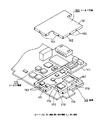
図4は、第2の筐体120の内部を示した図である。第2の筐体120は、上側筐体120aと下側筐体120bとに2分割することができ、その内部に回路基板140が配置してある。回路基板140には、携帯電話端末としての通信処理などに必要な回路が組であり、そのための回路部品151がハンダ付けなどで取付けてある。この場合、回路基板上の一部の回路部品については、比較的小型のシールドケースで直接覆うようにしてあり、そのシールドケースを構成する部材としてのシールド天板160が取付けられている。なお、第2の筐体120内の回路基板140のカメラユニット200を配置する箇所には、カメラユニット取付け用切り欠き部141を設けてあり、箱型形状のカメラユニット200が筐体120内に配置できるようにしてある。
FIG. 4 is a view showing the inside of the
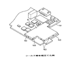
次に、図1,図2を参照して本例の回路基板140に構成されるシールドケース部について説明する。図1は、本例の回路基板140に構成されるシールドケース部を分解して示す図である。本例のシールドケースは、側板部と天板部とで構成されるようにしてある。即ち、回路基板140にハンダ付けで固定されるシールド部材(金属板)で構成されるシールド側板170と、そのシールド側板170に嵌合される金属板で構成されるシールド天板160とで、基板140上の所定箇所の回路部品152をシールドする構成としてある。
Next, the shield case part comprised in the
シールド側板170については、シールドケースのほぼ全周に渡って数ミリの高さで形成された側部171を有し、側部171の下端が回路基板140とハンダ付けで固定される。そして、側部171の上端から、内側に水平に数ミリ幅で上縁部172が形成してある。また、この上縁部172の2箇所を結ぶ形で梁部173が形成してあり、その梁部173のほぼ中央に、ほぼ円形で所定の面積の平面部174が形成させてある。側部171には、所定間隔で複数個の突起部175を形成させてある。
The
平面部174は、このシールド側板170を持ち上げた際に重心となるほぼ中央位置に配置してあり、円形の平面部174の面積としては、チップ部品を回路基板上に実装するチップ実装装置で吸着することができる面積としてある。
The
このシールド側板170に嵌合する天板部であるシールド天板160は、シールド部材(金属板)で形成されて、天板部161と、その天板部161の周縁部からほぼ全周に渡って直立した側部162とで構成される。側部162には、シールド側板170の側部171の突起部175に対応した位置に、透孔163を設けてある。この透孔163を突起部175に嵌合させることで、シールド側板170にシールド天板160を嵌合させた状態が維持される。
A
図2は、このシールド天板160をシールド側板170に嵌合させた状態を示した図である。このように嵌合させて組み立てることで、図1に示したシールドする必要のある回路部品152が、シールド天板160とシールド側板170とで構成されるシールドケースで覆われた状態となり、シールド効果が得られる。
FIG. 2 is a view showing a state in which the shield
このように構成したシールドケースによると、組み立てを簡単に行うことができる。即ち、組み立て時には、例えば回路基板140上の他の回路部品151,152をチップ実装装置で配置させるときに、シールド側板170についても、そのシールド側板170の梁部173に設けた平面部174を、チップ実装装置の吸着部で吸着させて持ち上げることで、チップ実装装置を使用して規定された位置に自動的に配置させることができる。基板上に配置されたシールド側板170は、回路基板140上の各回路部品をハンダ付けさせる工程時に、同時にハンダ付けで基板上に固定させれば良く、シールド側板170の取付けが容易に行える。そして、そのハンダ付けされたシールド側板170の突起部175に、シールド天板160の透孔163を嵌めるだけで、シールド天板160の取付け作業が行え、別体のシールドケース固定部材などを用意することなく、簡単に取付けが行える。
According to the shield case configured in this manner, assembly can be easily performed. That is, at the time of assembly, for example, when the
また、シールド側板170に取付けられたシールド天板160は、突起部175の透孔163への嵌合状態を外すだけで、簡単に取り外すことができる。従って、例えばシールドされた内部の回路部品152を交換する必要が生じた場合であっても、簡単に内部を開けることができ、リワーク性を向上させることができる。
Further, the shield
なお、上述した実施の形態では、また、シールド天板とシールド側板とは、シールド側板側に突起を設けて、シールド天板側にその突起と嵌合する透孔を設けるようにしたが、逆に、側板側に透孔を設けて、天板側に突起を設けて嵌合するようにしても良い。また、透孔の代わりに、突起と嵌合する凹部を設けるようにしても良い。 In the above-described embodiment, the shield top plate and the shield side plate are provided with projections on the shield side plate side, and through holes to be fitted with the projections on the shield top plate side. In addition, a through hole may be provided on the side plate side, and a protrusion may be provided on the top plate side for fitting. Moreover, you may make it provide the recessed part fitted with a processus | protrusion instead of a through-hole.
また、上述した実施の形態では、携帯電話端末に内蔵させる回路基板に適用したが、その他の各種小型の電子機器に内蔵させる回路基板にも適用できることは勿論である。 In the above-described embodiments, the circuit board is built in a mobile phone terminal. However, it is needless to say that the present invention can be applied to circuit boards built in other various small electronic devices.
100…携帯電話端末、110…第1の筐体、120…第2の筐体、130…レンズカバー、140…回路基板、141…カメラユニット取付け用切り欠き部、151,152…回路部品、160…シールド天板、161…天板部、162…側部、163…透孔、170…シールド側板、171…側部、172…上縁部、173…梁部、174…平面部、174…突起部、200…カメラユニット DESCRIPTION OF SYMBOLS 100 ... Cell-phone terminal, 110 ... 1st housing | casing, 120 ... 2nd housing | casing, 130 ... Lens cover, 140 ... Circuit board, 141 ... Notch part for camera unit attachment, 151, 152 ... Circuit component, 160 ... Shield top plate, 161 ... Top plate portion, 162 ... Side portion, 163 ... Through hole, 170 ... Shield side plate, 171 ... Side portion, 172 ... Upper edge portion, 173 ... Beam portion, 174 ... Plane portion, 174 ... Protrusion 200, camera unit
Claims (3)
前記回路基板上に固定された側部を有する枠状のシールド部材で形成されて、前記側部の上端からほぼ水平に伸びて所定面積の平面部を有する側板部と、
前記側板部に嵌合して、蓋をすることができる形状のシールド部材で形成された天板部とで構成された
シールドケース。 In the shield case attached to the place where the circuit that needs to be shielded on the circuit board is assembled,
A side plate portion formed of a frame-shaped shield member having a side portion fixed on the circuit board, and extending substantially horizontally from an upper end of the side portion and having a plane portion having a predetermined area;
A shield case comprising a top plate portion formed of a shield member having a shape that can be fitted to the side plate portion and can be covered.
前記平面部は、回路基板上のチップ部品を吸着するチップ実装装置で吸着できる面積を有し、前記側板部のほぼ重心となる位置に配置した
シールドケース。 The shield case according to claim 1,
The said planar part has the area which can be adsorb | sucked with the chip | tip mounting apparatus which adsorb | sucks the chip components on a circuit board, and is arrange | positioned in the position used as the substantially gravity center of the said side-plate part.
前記側板部と前記天板部の一方には嵌合用突起を設け、他方には嵌合用孔又は凹部を設けた
シールドケース。 The shield case according to claim 1,
One of the side plate portion and the top plate portion is provided with a fitting protrusion, and the other is provided with a fitting hole or recess.
Priority Applications (1)
| Application Number | Priority Date | Filing Date | Title |
|---|---|---|---|
| JP2003397645A JP2005159144A (en) | 2003-11-27 | 2003-11-27 | Shielding case |
Applications Claiming Priority (1)
| Application Number | Priority Date | Filing Date | Title |
|---|---|---|---|
| JP2003397645A JP2005159144A (en) | 2003-11-27 | 2003-11-27 | Shielding case |
Publications (2)
| Publication Number | Publication Date |
|---|---|
| JP2005159144A true JP2005159144A (en) | 2005-06-16 |
| JP2005159144A5 JP2005159144A5 (en) | 2006-12-28 |
Family
ID=34722745
Family Applications (1)
| Application Number | Title | Priority Date | Filing Date |
|---|---|---|---|
| JP2003397645A Pending JP2005159144A (en) | 2003-11-27 | 2003-11-27 | Shielding case |
Country Status (1)
| Country | Link |
|---|---|
| JP (1) | JP2005159144A (en) |
Cited By (7)
| Publication number | Priority date | Publication date | Assignee | Title |
|---|---|---|---|---|
| JP2007266024A (en) * | 2006-03-27 | 2007-10-11 | Kyocera Corp | Electronic equipment and shield case |
| JP2007335672A (en) * | 2006-06-15 | 2007-12-27 | Murata Mfg Co Ltd | Shielding structure |
| JP2008028342A (en) * | 2006-07-25 | 2008-02-07 | Toshiba Corp | Shield structure, and mobile terminal including shield structure |
| JP2008112903A (en) * | 2006-10-31 | 2008-05-15 | Matsushita Electric Ind Co Ltd | Manufacturing method of mounting substrate, and component mounting machine |
| JP2008300472A (en) * | 2007-05-30 | 2008-12-11 | Kyocera Corp | Shield case for electronic apparatus and electronic apparatus |
| CN114023706A (en) * | 2022-01-06 | 2022-02-08 | 江苏明芯微电子股份有限公司 | Electronic chip magnetic field shielding structure capable of reducing occupied space |
| US11686842B2 (en) | 2019-06-17 | 2023-06-27 | Aisin Corporation | Sonar unit |
-
2003
- 2003-11-27 JP JP2003397645A patent/JP2005159144A/en active Pending
Cited By (8)
| Publication number | Priority date | Publication date | Assignee | Title |
|---|---|---|---|---|
| JP2007266024A (en) * | 2006-03-27 | 2007-10-11 | Kyocera Corp | Electronic equipment and shield case |
| JP2007335672A (en) * | 2006-06-15 | 2007-12-27 | Murata Mfg Co Ltd | Shielding structure |
| JP2008028342A (en) * | 2006-07-25 | 2008-02-07 | Toshiba Corp | Shield structure, and mobile terminal including shield structure |
| JP2008112903A (en) * | 2006-10-31 | 2008-05-15 | Matsushita Electric Ind Co Ltd | Manufacturing method of mounting substrate, and component mounting machine |
| JP2008300472A (en) * | 2007-05-30 | 2008-12-11 | Kyocera Corp | Shield case for electronic apparatus and electronic apparatus |
| US11686842B2 (en) | 2019-06-17 | 2023-06-27 | Aisin Corporation | Sonar unit |
| CN114023706A (en) * | 2022-01-06 | 2022-02-08 | 江苏明芯微电子股份有限公司 | Electronic chip magnetic field shielding structure capable of reducing occupied space |
| CN114023706B (en) * | 2022-01-06 | 2022-03-18 | 江苏明芯微电子股份有限公司 | Electronic chip magnetic field shielding structure capable of reducing occupied space |
Similar Documents
| Publication | Publication Date | Title |
|---|---|---|
| JP4668036B2 (en) | Mounting structure for FPC of image sensor | |
| US20090016039A1 (en) | Structure And Method For Attaching Shield Case To Circuit Board, Electronic Component Module And Portable Telephone | |
| KR101101658B1 (en) | endoscopic camera module package and method for manufacturing the same | |
| TW595129B (en) | Electronic device | |
| TWI663463B (en) | Driving mechanism | |
| US8283814B2 (en) | Voice coil motor assembly with contamination prevention means | |
| US9436062B2 (en) | Camera body | |
| KR101422954B1 (en) | Camera module | |
| GB2413435A (en) | Camera lens module and method of assembly thereof | |
| JP2007274624A (en) | Camera module | |
| KR20120015105A (en) | Camera module | |
| JP2016130746A (en) | Camera module and manufacturing method of the same | |
| US20070263116A1 (en) | Solid-state image pickup device and electronic device | |
| US7387255B2 (en) | Portable terminal apparatus | |
| JP2005159144A (en) | Shielding case | |
| KR100702601B1 (en) | Jig for camera module and fabricating method therefore | |
| US8708502B2 (en) | Projection type image display apparatus with shielded circuit board | |
| TW202225755A (en) | Camera module and electronic device | |
| US20060055812A1 (en) | Optical equipment having image pickup element | |
| CN107613047B (en) | Manufacturing method of electronic assembly, electronic assembly and electronic device | |
| KR20120118894A (en) | Camera module device | |
| CN107566558B (en) | Method for manufacturing electronic assembly | |
| TWI448135B (en) | Moblie phone | |
| JP2007208339A (en) | Portable electronic apparatus | |
| EP1150475A2 (en) | Holder and portable telephone with the holder |
Legal Events
| Date | Code | Title | Description |
|---|---|---|---|
| A521 | Written amendment |
Effective date: 20061110 Free format text: JAPANESE INTERMEDIATE CODE: A523 |
|
| A621 | Written request for application examination |
Free format text: JAPANESE INTERMEDIATE CODE: A621 Effective date: 20061110 |
|
| A977 | Report on retrieval |
Effective date: 20090422 Free format text: JAPANESE INTERMEDIATE CODE: A971007 |
|
| A131 | Notification of reasons for refusal |
Effective date: 20090428 Free format text: JAPANESE INTERMEDIATE CODE: A131 |
|
| A521 | Written amendment |
Effective date: 20090617 Free format text: JAPANESE INTERMEDIATE CODE: A523 |
|
| A131 | Notification of reasons for refusal |
Effective date: 20090804 Free format text: JAPANESE INTERMEDIATE CODE: A131 |
|
| A521 | Written amendment |
Effective date: 20090924 Free format text: JAPANESE INTERMEDIATE CODE: A523 |
|
| A02 | Decision of refusal |
Effective date: 20091201 Free format text: JAPANESE INTERMEDIATE CODE: A02 |