JP2005143114A - Switching circuit for performing clock interpolation - Google Patents
Switching circuit for performing clock interpolation Download PDFInfo
- Publication number
- JP2005143114A JP2005143114A JP2004320690A JP2004320690A JP2005143114A JP 2005143114 A JP2005143114 A JP 2005143114A JP 2004320690 A JP2004320690 A JP 2004320690A JP 2004320690 A JP2004320690 A JP 2004320690A JP 2005143114 A JP2005143114 A JP 2005143114A
- Authority
- JP
- Japan
- Prior art keywords
- switching circuit
- frequency
- signal
- input signal
- digital
- Prior art date
- Legal status (The legal status is an assumption and is not a legal conclusion. Google has not performed a legal analysis and makes no representation as to the accuracy of the status listed.)
- Pending
Links
Images


Classifications
-
- H—ELECTRICITY
- H03—ELECTRONIC CIRCUITRY
- H03L—AUTOMATIC CONTROL, STARTING, SYNCHRONISATION, OR STABILISATION OF GENERATORS OF ELECTRONIC OSCILLATIONS OR PULSES
- H03L7/00—Automatic control of frequency or phase; Synchronisation
- H03L7/06—Automatic control of frequency or phase; Synchronisation using a reference signal applied to a frequency- or phase-locked loop
- H03L7/16—Indirect frequency synthesis, i.e. generating a desired one of a number of predetermined frequencies using a frequency- or phase-locked loop
-
- H—ELECTRICITY
- H03—ELECTRONIC CIRCUITRY
- H03L—AUTOMATIC CONTROL, STARTING, SYNCHRONISATION, OR STABILISATION OF GENERATORS OF ELECTRONIC OSCILLATIONS OR PULSES
- H03L7/00—Automatic control of frequency or phase; Synchronisation
- H03L7/06—Automatic control of frequency or phase; Synchronisation using a reference signal applied to a frequency- or phase-locked loop
- H03L7/08—Details of the phase-locked loop
- H03L7/099—Details of the phase-locked loop concerning mainly the controlled oscillator of the loop
- H03L7/0991—Details of the phase-locked loop concerning mainly the controlled oscillator of the loop the oscillator being a digital oscillator, e.g. composed of a fixed oscillator followed by a variable frequency divider
- H03L7/0994—Details of the phase-locked loop concerning mainly the controlled oscillator of the loop the oscillator being a digital oscillator, e.g. composed of a fixed oscillator followed by a variable frequency divider comprising an accumulator
-
- G—PHYSICS
- G06—COMPUTING; CALCULATING OR COUNTING
- G06F—ELECTRIC DIGITAL DATA PROCESSING
- G06F1/00—Details not covered by groups G06F3/00 - G06F13/00 and G06F21/00
- G06F1/02—Digital function generators
- G06F1/03—Digital function generators working, at least partly, by table look-up
- G06F1/0321—Waveform generators, i.e. devices for generating periodical functions of time, e.g. direct digital synthesizers
- G06F1/0328—Waveform generators, i.e. devices for generating periodical functions of time, e.g. direct digital synthesizers in which the phase increment is adjustable, e.g. by using an adder-accumulator
Abstract
Description
本発明は、第1の周波数を有する入力信号を処理して、周波数が入力信号の第1の周波数の倍数である少なくとも1つの出力信号を出力するスイッチング回路および方法に関するものである。 The present invention relates to a switching circuit and method for processing an input signal having a first frequency and outputting at least one output signal whose frequency is a multiple of the first frequency of the input signal.
印刷機の制御は、今日、精度の要求が高まっているために、印刷機の回転部品に回転検出器を使用することなしには考えることができない。特に、個別駆動式の個々の印刷ユニットの間に一貫した機械的な駆動接続を備えていない印刷機では、互いに機械的に連結されていない印刷ユニットを正しい見当で作動させることができるようにするために、駆動される個々の印刷胴すべてに回転角検出器を設けることが必要である。このとき回転角検出器は、時間に対してプロットされた印刷胴等の回転部品の回転角を検出して、この回転角を、印刷機の機械制御部に送ることができる電気信号に変換する。しかし最近では、回転検出器は印刷胴を同期化するために必要なばかりでなく、版露光器やいわゆるDI印刷機において、すなわち、版胴が機械内部でたとえばレーザにより書き込まれ、それによって画像付けされるオフセット印刷機において、画像付けプロセスを制御するのにも必要となっている。このような画像付けを十分に正確に行えるようにするためには、回転する版胴で用いられる回転角検出器の信号が、高い解像度を備えていなくてはならない。 The control of a printing press cannot be considered without using a rotation detector for the rotating parts of the printing press due to the increasing demand for accuracy today. In particular, in a printing press that does not have a consistent mechanical drive connection between individually driven individual printing units, it is possible to operate printing units that are not mechanically coupled to each other with the correct registration. Therefore, it is necessary to provide a rotation angle detector for every driven printing cylinder. At this time, the rotation angle detector detects the rotation angle of a rotating part such as a printing cylinder plotted against time, and converts this rotation angle into an electrical signal that can be sent to the machine control unit of the printing press. . More recently, however, rotation detectors are not only necessary to synchronize the printing cylinder, but also in plate exposure machines or so-called DI printing machines, i.e. the printing cylinder is written inside the machine, for example by means of a laser, whereby imaging is performed. In an offset printing press, it is also necessary to control the imaging process. In order to be able to perform such imaging sufficiently accurately, the signal of the rotation angle detector used in the rotating plate cylinder must have a high resolution.
回転角検出器では、基本的に、物理的な解像度と補間された解像度とを区別することができる。回転検出器が1回転についてたとえば360ステップの下位区分を有しているとすると、このことは、回転検出器の物理的な解像度に相当している。この信号を電子回路で補間によってもっと解像度の高いフォーマットに変換することができ、この場合には誤差が発生するのが通常である。角度補間をするために、従来技術からいくつかの方法が公知となっている。高い解像度の回転角情報を生成するために駆動工学から公知となっている1つの解決法は、サイン/コサイン出力信号を出す回転検出器を利用し、この出力信号を基にして、アークタンジェント法を用いて瞬間の角度を算出することにある。所望の高い解像度をサイン/コサイン回転検出器で実現するためには、この回転検出器が非常に高い物理的なピッチ数で作動しなければならない。このような方法では、100を超える補間係数は実現するのが非常に難しいからである。そのためには設計的に非常に高いコストがかかり、したがって相応に高価になる。そのため、このような回転検出器で解像度を高めるためにしばしば利用される補間法は、適用される補間係数の変更がまったく不可能であるか、または非常に大まかな変更しか可能でなく、多くの場合、補間係数は整数に限られている。ところが印刷機で版胴を画像付けするときには明確な角度位置でクロックを生成しなければならず、このことは、上記に加えてさらに可変な有理補間係数を必要とする。 In the rotation angle detector, it is basically possible to distinguish between physical resolution and interpolated resolution. If the rotation detector has a subdivision of 360 steps per rotation, for example, this corresponds to the physical resolution of the rotation detector. This signal can be converted into a higher resolution format by interpolation with an electronic circuit, and in this case, an error usually occurs. Several methods are known from the prior art for angle interpolation. One solution known from drive engineering to generate high resolution rotation angle information is to use a rotation detector that produces a sine / cosine output signal, and based on this output signal, the arctangent method It is to calculate the instantaneous angle using. In order to achieve the desired high resolution with a sine / cosine rotation detector, the rotation detector must operate at a very high physical pitch number. This is because it is very difficult to realize an interpolation coefficient exceeding 100 by such a method. This is very expensive in terms of design and is therefore correspondingly expensive. As a result, the interpolation methods often used to increase the resolution in such rotation detectors cannot change the applied interpolation factor at all, or can only make very rough changes, and many In this case, the interpolation coefficient is limited to an integer. However, when imaging a plate cylinder on a printing press, the clock must be generated at a well-defined angular position, which requires a more variable rational interpolation factor in addition to the above.
角度同期された高い解像度のクロック信号を生成するために従来技術から公知となっている別の方法は、たとえば二進法のクロック信号を周波数逓倍するために用いられるいわゆる位相制御回路(PLL)と接続された、TTL回転検出器(TTLは”Transistor Transistor Logik”(トランジスタ・トランジスタ・ロジック)の略)とも呼ばれる、二進法の出力信号を出すデジタルエンコーダを利用することにある。PLLという概念は”Phase Locked Loop”(フェイズロックループ)を意味しており、出力信号が入力信号と同じ位相になるように適応制御される制御回路である。この場合、周波数が、回転検出器の二進法の出力信号の周波数の任意の倍数であるクロック出力信号を生成することができ、その際に位相情報が失われることがない。回転検出器の二進法の出力信号の周波数の有理倍数が要求される場合には、”Fractional−N”(フラクショナルN)の名称で知られる技術が適用される。この場合、位相制御回路のフィードバック分路に、分周比の時間的な変更を可能にするプログラミング可能な分周器が設けられる。分周比の時間的な変更によって、位相制御回路の入力周波数を、時間的な平均値を中心として有理係数で逓倍することができるが、この位相制御回路は原則として整数によってしか分割することができない。たとえば出力信号を係数10.5だけ高めたいときは、時間を通して平均したときに10.5の係数が得られるように、分周器の分周比を10と11へ交互に変更しなければならない。「フラクショナルN」技術の場合、特に、システム誤差が原理的に発生することが欠点となる。位相制御回路の位相検出器の出力部でプログラミング可能な分周器の分周比を変更すると、外乱が発生するからである。 Another method known from the prior art for generating an angle-synchronized high resolution clock signal is connected to a so-called phase control circuit (PLL) which is used, for example, to multiply the frequency of a binary clock signal. Another object is to use a digital encoder that outputs a binary output signal, which is also called a TTL rotation detector (TTL is an abbreviation of “Transistor Transistor Logic”). The concept of PLL means “Phase Locked Loop”, which is a control circuit that is adaptively controlled so that the output signal has the same phase as the input signal. In this case, it is possible to generate a clock output signal whose frequency is an arbitrary multiple of the frequency of the binary output signal of the rotation detector, and no phase information is lost. When a rational multiple of the frequency of the binary output signal of the rotation detector is required, a technique known by the name “Fractional-N” (fractional N) is applied. In this case, a programmable frequency divider is provided in the feedback shunt of the phase control circuit, which allows the frequency division ratio to be changed over time. By changing the frequency division ratio over time, the input frequency of the phase control circuit can be multiplied by a rational factor centered on the temporal average value. In principle, this phase control circuit can only be divided by integers. Can not. For example, if the output signal is to be increased by a factor of 10.5, the divider ratio must be alternately changed to 10 and 11 so that a factor of 10.5 is obtained when averaged over time. . In the case of the “fractional N” technique, the disadvantage is in particular that system errors occur in principle. This is because disturbance occurs when the frequency division ratio of the frequency divider that can be programmed at the output portion of the phase detector of the phase control circuit is changed.
回転検出器の出力クロックが周期時間にわたって測定され、次いで、出力クロックの逓倍された周波数が算出される周波数逓倍方法も、類似の取り組みを追求するものである。出力クロックを正しい位相で入力クロックと組み合わせるために、位相制御回路がこの場合にも用いられ、この位相制御回路は、出力信号における位相誤差の修正を絶えず行うために、入力信号の周波数を直接制御するように構成されている。この方法は特許文献1に詳細に記載されている。 A frequency multiplication method in which the output clock of the rotation detector is measured over a period of time and then the multiplied frequency of the output clock is calculated follows a similar approach. A phase control circuit is also used in this case to combine the output clock with the input clock in the correct phase, which directly controls the frequency of the input signal to continually correct for phase errors in the output signal. Is configured to do. This method is described in detail in Patent Document 1.
印刷機製造の分野では、特許文献2より、入力信号の倍数をもつ出力クロック信号の生成が通常のPLL周波数逓倍回路によって行われる、TTL回転検出器の二進法のクロック信号を周波数逓倍する方法が公知となっている。周波数逓倍回路の出力信号は、いわゆるDDS周波数発生器の供給クロック信号となる。DDSは”Direct Digital Synthesis”(ダイレクトデジタル合成)の略である。しかしこの設計形態は、このような通常の位相制御回路ではDDS周波数発生器への供給クロックの生成が非常に限られた周波数領域でしか機能しないという欠点がある。
そこで本発明の目的は、振動信号から補間された高い解像度の出力信号を生成し、その際に、従来技術の上述した欠点を回避することである。 It is therefore an object of the present invention to generate a high resolution output signal interpolated from the vibration signal, thereby avoiding the aforementioned drawbacks of the prior art.
この目的は、請求項1および15によって本発明により解決される。本発明のその他の実施態様は、従属請求項および図面から読み取ることができる。 This object is solved according to the invention by claims 1 and 15. Other embodiments of the invention can be taken from the dependent claims and the drawings.
本発明のスイッチング回路および本発明の方法により、一定の周波数を有する振動信号を逓倍することが容易に可能である。スイッチング回路は、アナログ技術で構成されていてもデジタル技術で構成されていてもよい。 By the switching circuit of the present invention and the method of the present invention, it is possible to easily multiply the vibration signal having a constant frequency. The switching circuit may be configured by analog technology or digital technology.
本発明の第1の実施態様では、スイッチング回路がデジタル式に構成されている。このデジタル構造は、入力信号の周波数を測定できるという位相制御回路(PLL)の特性を利用したものである。位相制御回路がラッチング状態(eingerasteten)で作動している限り、位相情報が失われることはないので、位相制御回路の出力信号は同じ位相で入力信号の周波数に比例する。さらに、位相制御回路の出力信号は周波数逓倍器によって逓倍されて発振器の入力部に転送され、この発振器の出力信号が、所望の出力クロックの周波数を有している。このようなシステムでは、出力クロックの位相はもはや閉ループ制御(geregelt)されるのではなく、開ループ制御(gesteuert)されるにすぎず、したがって、本方法は完全にデジタル式のシステムで実現されなくてはならない。本発明の大きな利点は、「フラクショナルN」技術の場合のようにシステム誤差を修正するために追加の実現コストを払わなくてもすみ、その一方で、回転検出器の所望の高い分解能を実現できるという点にある。さらに、印刷胴の画像付けするときに、明確な角度位置に対応するクロック信号を出力することができる。しかもデジタルスイッチング回路は、広い周波数領域をカバーすることができるという利点や、該当するデジタルモジュールを単にプログラミングするだけで、スイッチング回路を非常にフレキシブルに設計することができるという利点をもたらす。 In the first embodiment of the present invention, the switching circuit is configured digitally. This digital structure utilizes the characteristic of a phase control circuit (PLL) that can measure the frequency of an input signal. As long as the phase control circuit is operating in the latching state, no phase information is lost, so the output signal of the phase control circuit is in the same phase and proportional to the frequency of the input signal. Further, the output signal of the phase control circuit is multiplied by a frequency multiplier and transferred to the input part of the oscillator, and the output signal of the oscillator has a desired output clock frequency. In such a system, the phase of the output clock is no longer closed-loop controlled, but only open-loop controlled, and thus the method is not implemented in a fully digital system. must not. A significant advantage of the present invention is that no additional implementation cost is required to correct system errors as in the case of “fractional N” technology, while the desired high resolution of the rotation detector can be achieved. It is in that point. Further, when an image of the printing cylinder is applied, a clock signal corresponding to a clear angular position can be output. Moreover, the digital switching circuit has the advantage that it can cover a wide frequency range, and the switching circuit can be designed very flexibly by simply programming the corresponding digital module.
本発明の別の実施態様では、PLL周波数測定回路が周波数逓倍器を介してデジタル発振器の入力部に接続されており、その出力信号がデジタルスイッチング回路の出力信号である。すでに述べたように、位相制御回路の発振器は、周波数逓倍に引き続いて、開ループ制御されるにすぎない別の発振器と同期化されなくてはならないので、本発明のスイッチング回路は完全にデジタル式の技術でしか実現することができない。この理由から、周波数逓倍器の出力部にある発振器もデジタル発振器であることが必要である。 In another embodiment of the present invention, the PLL frequency measurement circuit is connected to the input of the digital oscillator via a frequency multiplier, and the output signal is the output signal of the digital switching circuit. As already mentioned, since the oscillator of the phase control circuit must be synchronized with another oscillator that is only open-loop controlled following frequency multiplication, the switching circuit of the present invention is completely digital. It can only be realized with this technology. For this reason, the oscillator at the output of the frequency multiplier must also be a digital oscillator.
この場合にはさらに、PLL周波数測定回路にあるデジタル発振器と、周波数逓倍器を介してPLL周波数測定回路に接続されたデジタル発振器とが、同じシステムクロック信号で制御可能であるのが有利である。両方のデジタル発振器は、同じシステムクロックが供給される場合にのみ同期して作動することができる。完全にデジタル式のシステム構造によってのみ、このような同じシステムクロックを両方の発振器で使用することが可能である。 In this case, it is further advantageous that the digital oscillator in the PLL frequency measuring circuit and the digital oscillator connected to the PLL frequency measuring circuit via a frequency multiplier can be controlled with the same system clock signal. Both digital oscillators can only operate synchronously if the same system clock is supplied. Only with a completely digital system structure such an identical system clock can be used with both oscillators.
本発明の別の有利な実施態様では、デジタルスイッチング回路の入力信号が、2チャンネル回転検出器のデジタル出力信号である。2チャンネル回転検出器では、両方の出力チャンネルが互いに90度だけ位相がずれた状態で通っている。(1回転を一義的に分解することはデジタルエンコーダにはできない。それができるのは絶対値発生器だけである。)そして2チャンネル回転検出器のデジタル出力信号を、デジタルスイッチング回路で処理するために使用することができる。この場合、分解能が特別に高くはない、市販されている通常のデジタルインクリメンタルエンコーダを利用することができ、このことはコストを大幅に引き下げる。 In another advantageous embodiment of the invention, the input signal of the digital switching circuit is the digital output signal of the two-channel rotation detector. In a two-channel rotation detector, both output channels pass with a phase shift of 90 degrees from each other. (It is not possible for a digital encoder to unambiguously resolve one rotation. Only an absolute value generator can do that.) And to process the digital output signal of a two-channel rotation detector with a digital switching circuit Can be used for In this case, a commercially available normal digital incremental encoder with a resolution that is not particularly high can be used, which greatly reduces the cost.
さらに、PLL周波数測定回路が、2つまたは3つ以上の周波数逓倍器を介して、2つまたは3つ以上の付属のデジタル発振器の入力部に接続されており、その出力クロック信号がスイッチング回路の出力信号であることが好ましい。それにより、位相結合された状態で共通の入力信号になる、異なる周波数の出力信号を並行して供給することが可能である。この場合、接続されているすべてのデジタル発振器がシステムクロックに拘束される。 Furthermore, a PLL frequency measurement circuit is connected to the input of two or more attached digital oscillators via two or more frequency multipliers, and its output clock signal is connected to the switching circuit. An output signal is preferred. As a result, it is possible to supply in parallel output signals of different frequencies that become a common input signal in a phase-coupled state. In this case, all connected digital oscillators are bound to the system clock.
さらに、デジタルスイッチング回路が、プログラマブル・ロジックデバイスによって実現されることが意図される。このようなシステムは、プログラマブル・ロジックデバイス、たとえばCPLD(Complex Programable Logic Device、コンプレックス・プログラマブル・ロジック・デバイス)やFPGA(Field Programable Gate Array、フィールド・プログラマブル・ゲートアレイ)である。 Furthermore, it is contemplated that the digital switching circuit is realized by a programmable logic device. Such systems are programmable logic devices such as CPLD (Complex Programmable Logic Device) and FPGA (Field Programmable Gate Array, Field Programmable Gate Array).
さらに、これに代えて、デジタルスイッチング回路が信号プロセッサによって実現されることが意図される。信号プロセッサはロジックデバイスとは異なり、デジタル信号処理の分野における特別な役割に合わせて設計されている。DSPもしくはロジックデバイスに代えて、またはこれに加えて、ASICを使用することができる。ASIC(Application Specific Integrated Circuit、特定用途向け集積回路)は特定の利用目的のために製作されており、すなわち非常に特殊化したモジュールである。あるいは、デジタルスイッチング回路の一部がプログラマブル・ロジックデバイスで具体化されており、デジタルスイッチング回路の別の部分は信号プロセッサまたはASICで具体化することも可能である。このようにして、個々のデジタルモジュールの利点を互いに組み合わせることができる。 Further alternatively, it is contemplated that the digital switching circuit is implemented by a signal processor. Unlike logic devices, signal processors are designed for a special role in the field of digital signal processing. An ASIC can be used in place of or in addition to a DSP or logic device. An ASIC (Application Specific Integrated Circuit) is made for a specific purpose of use, i.e. a highly specialized module. Alternatively, a portion of the digital switching circuit may be embodied with a programmable logic device and another portion of the digital switching circuit may be embodied with a signal processor or ASIC. In this way, the advantages of the individual digital modules can be combined with each other.
周波数逓倍器は、有理補間係数で逓倍をすることが好ましい。有理補間係数を用いることで、回転検出器の角度信号の解像度をほぼ無段階に規定することができる。というのも、二進法の量子化だけが解像度を制限するからである。解像度の無段階に可変な構造によって初めて、物理的な解像度の整数倍に相当しない明確な角度位置でクロック信号を生成することが可能となる。このことは、たとえば印刷機での版胴の画像付けのときに必要なので、本発明は、印刷機またはその他の被印刷体処理機械の回転検出器からの角度信号を処理するのに特に適している。 The frequency multiplier is preferably multiplied by a rational interpolation coefficient. By using the rational interpolation coefficient, the resolution of the angle signal of the rotation detector can be defined almost steplessly. This is because only binary quantization limits the resolution. A clock signal can be generated at a clear angular position that does not correspond to an integral multiple of the physical resolution only by a structure with a stepless change in resolution. Since this is necessary, for example, when printing plate cylinders on a printing press, the present invention is particularly suitable for processing angular signals from a rotation detector of a printing press or other substrate processing machine. Yes.
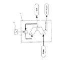
図1は、印刷機12で使用する場合の本発明によるデジタルスイッチング回路の原理的な構造を示している。このデジタルスイッチング回路は、一方では、回転検出器の出力信号を入力信号Inとして入力し、入力信号Inと位相結合された信号fを出力するPLL周波数測定回路6で構成されている。PLL周波数測定回路6は、入力信号Inと信号fとの間の位相差を判定する位相検出器と、これと接続されたコントローラ5で構成されている。閉ループ制御される信号fは、デジタル発振器1を有するフィードバック分路へ供給される。PLL周波数測定回路6によって周波数逓倍なしに測定され、引き続いて周波数逓倍器3で任意の補間係数i1で逓倍された信号fの値は、第2のデジタル発振器1の入力部に印加され、このデジタル発振器が出力信号Outを生成する。この変形例では、出力クロックOutの位相はもはや閉ループ制御されず、開ループ制御されるだけなので、完全にデジタル式のシステムとしてしか具体化することができない。開ループ制御されるデジタル発振器1の両方のクロックの位相は、同じシステムクロック2の供給を受けることによって互いに同期化されており、このことは、図1のブロック図では小さなブロック2が記号で図示されている。PLL周波数測定回路6には複数の周波数逓倍器3とデジタル発振器1が接続されていてよく、それにより、補間係数i1からinが異なっていれば、異なる周波数をもつ出力信号outを出力することができる。これらの出力信号outは並行して利用することができ、すべて入力信号Inと位相結合されている。
FIG. 1 shows the basic structure of a digital switching circuit according to the present invention when used in a
入力信号Inの周波数の測定を、どうしてマイクロコントローラ等を用いて直接行わないのかという疑問が浮かぶが、その理由は、PLL周波数測定回路6によって周波数が位相制御されながら測定されることにある。周波数と位相の間には不可分の関係があるため、簡単な周波数測定では、たとえばデジタル乗算の量子化雑音や、入力信号の時間的な量子化といった誤差が制御不能に合算されてしまい、すなわち、印刷機12の回転部品の回転角に関する情報が失われてしまう。これとは異なり、PLL周波数測定回路6は位相情報を失うことなく入力信号Inの周波数を測定する。というのも、PLL周波数測定回路6がラッチング状態で作動している限り、位相が繰り返して検知されるからである。この事実は数学的に表現することができる。測定される周波数は、本当の成分fin(t)と誤差成分fe(t)とで成り立っているので、出力信号の周波数fout(t)については、次式が成立する。
The question arises as to why the frequency of the input signal In is not directly measured using a microcontroller or the like. The reason is that the frequency is measured by the PLL

もしくは積分の後、その位相について次式が成立する。 Or after integration, the following equation holds for the phase.
PLL周波数測定回路6は、fe(t)が定常成分を含まず、φe(t)が見積可能な限度内に収まるように作用する。簡単な周波数測定の場合には位相制御が行われず、誤差を限定できなくなる。したがって、PLL周波数測定回路6の周波数測定特性は、周波数が第1のクロック信号Inの周波数の有理倍数iであり、かつ、位相が第1のクロック信号Inの位相に結合されたクロック信号Outを生成するために直接利用することができる。
The PLL
図3では、図1に示す完全にデジタル式のシステムが、プログラマブル・ロジックデバイス7の内部で実現されている。このシステムを信号プロセッサの内部で具体化したり、あるいはこの両方の実施形態を組み合わせて、さまざまなコンポーネントをプログラマブル・ロジックデバイス7と信号プロセッサに振り分けることも可能である。図3では、ここには図示しない回転検出器の両方のチャンネルA,Bが左側から入ってきている。両方の信号は90°だけ電気的に位相がずれている。逓倍回路8が、両方のチャンネルAおよびBの立下りエッジと立上りエッジを評価する。こうして生成された信号が、入力信号Inの周波数を測定するPLL周波数測定回路6への入力信号Inを形成する。PLL周波数測定回路6の後に本来のクロック生成スイッチング回路10が続いており、ここで、PLL周波数測定回路6によって供給された測定値fが周波数逓倍器3により相応の補間係数iで増減されたうえで、出力信号Outを実効クロックCLK outとして生成するデジタル発振器1の入力部に送られる。ロジックデバイス7のレジスタバンク11には、全回路の読出し可能・書込み可能なパラメータがあるので、全回路を汎用的に利用可能である。
In FIG. 3, the fully digital system shown in FIG. 1 is implemented inside the programmable logic device 7. The system can be embodied within the signal processor, or a combination of both embodiments can distribute the various components to the programmable logic device 7 and the signal processor. In FIG. 3, both channels A and B of a rotation detector (not shown) are entered from the left side. Both signals are electrically out of phase by 90 °. A multiplier circuit 8 evaluates the falling and rising edges of both channels A and B. The signal thus generated forms the input signal In to the PLL
図2にはデジタル発振器1のブロック図を見ることができ、PLL周波数測定回路6の追従する発振器1と、クロック生成スイッチング回路10の発振器1とはいずれも簡単な位相累算器として構成されている。このような累算器では、たとえば発振器1の周波数fを表す二進ワードfwが、ここではfclkであるシステムクロック2と累算される。クロック出力CLK outとして、回路は累算器のオーバーフロービットを利用する。出力信号CLK outの周波数foscは次式の値となる。
A block diagram of the digital oscillator 1 can be seen in FIG. 2. The oscillator 1 that the PLL
これに加えて、位相累算器の最新の値が印加される出力部Pがある。このことは、以下に説明するような位相検知機能の簡単な回路工学上の具体化を可能にする。PLL周波数測定回路6の入力信号Inと、開ループ制御される追従する発振器1の出力クロックCLK outとの間の位相ずれを測定する位相検知器4をなすのは、PLL周波数測定回路6の入力信号による、追従する発振器1の位相信号Pの走査である。すなわち、入力パルスがロジックデバイス7のレジスタに位相累積器の内容を書き込む。このレジスタ内容は、追従する発振器1の入力信号Inと出力信号CLK outの間の位相ずれを、2の補数で表している。
In addition to this, there is an output P to which the latest value of the phase accumulator is applied. This allows a simple circuit engineering implementation of the phase detection function as described below. The
コントローラ9はデジタル計算回路、たとえばデジタルPIコントローラ9として具体化される。PLL周波数測定回路6の追従する発振器1の周波数ワードを補間係数iで増減する周波数逓倍器3が本来の角度補間であり、ここでは入力信号Inの周波数fが逓倍される。増減演算の実行は、n×nビット乗算として行われる。
The
1 デジタル発振器
2 システムクロック信号
3 周波数逓倍器
4 位相検知器
5 コントローラ
6 PLL周波数測定回路
7 プログラマブル・ロジックデバイス
8 逓倍回路
9 デジタルPIコントローラ
10 クロック生成スイッチング回路
11 レジスタバンク
12 印刷機
In 入力信号
Out 出力信号
P 位相信号
f 周波数信号
CLK out 出力クロック信号
i 補間係数
A 回転検出器のチャンネル1
B 回転検出器のチャンネル2
DESCRIPTION OF SYMBOLS 1
Claims (17)
前記入力信号(In)がPLL周波数測定回路(6)で周波数と位相に関して測定可能であり、測定された入力信号(In)が少なくとも1つの周波数逓倍器(3)およびこれに後続する発振器(1)によって逓倍可能であることを特徴とするスイッチング回路。 In a switching circuit (7) that processes an input signal (In) having a first frequency and outputs at least one output signal (Out) whose frequency is a multiple of the first frequency of the input signal (In). ,
The input signal (In) is measurable with respect to frequency and phase in a PLL frequency measurement circuit (6), and the measured input signal (In) is at least one frequency multiplier (3) followed by an oscillator (1 A switching circuit characterized by being capable of being multiplied by a).
前記入力信号(In)をPLL周波数測定回路(6)で周波数と位相に関して測定し、測定された入力信号(In)を少なくとも1つの周波数逓倍器(3)およびこれに後続する発振器(1)によって逓倍することを特徴とする方法。 In a method of processing an input signal (In) having a first frequency and outputting at least one output signal (Out) whose frequency is a multiple of the first frequency of the input signal (In).
The input signal (In) is measured with respect to frequency and phase by a PLL frequency measurement circuit (6), and the measured input signal (In) is measured by at least one frequency multiplier (3) and an oscillator (1) subsequent thereto. A method characterized by multiplying.
The method according to claim 16, wherein a rotation angle input signal (In) from a rotation detector is processed as the input signal (In).
Applications Claiming Priority (1)
| Application Number | Priority Date | Filing Date | Title |
|---|---|---|---|
| DE10351218 | 2003-11-03 |
Publications (2)
| Publication Number | Publication Date |
|---|---|
| JP2005143114A true JP2005143114A (en) | 2005-06-02 |
| JP2005143114A5 JP2005143114A5 (en) | 2007-07-12 |
Family
ID=34530058
Family Applications (1)
| Application Number | Title | Priority Date | Filing Date |
|---|---|---|---|
| JP2004320690A Pending JP2005143114A (en) | 2003-11-03 | 2004-11-04 | Switching circuit for performing clock interpolation |
Country Status (4)
| Country | Link |
|---|---|
| US (1) | US7898342B2 (en) |
| JP (1) | JP2005143114A (en) |
| CN (1) | CN100506535C (en) |
| DE (1) | DE102004050621B4 (en) |
Families Citing this family (8)
| Publication number | Priority date | Publication date | Assignee | Title |
|---|---|---|---|---|
| DE102004007069A1 (en) * | 2004-02-13 | 2005-08-25 | Goss International Montataire S.A. | Rotation element for folding mechanism of printing machine, with encoder generating first periodical signal during element rotation, with encoder coupled to evaluator with synthesizer(s) |
| AT8256U3 (en) * | 2005-12-29 | 2007-01-15 | Avl List Gmbh | METHOD AND DEVICE FOR PROVIDING A HIGH-RELEASE WINKELMARK SIGNAL |
| BRPI0805426A2 (en) * | 2007-12-19 | 2009-08-18 | Vestas Wind Sys As | electric generator system with intelligent positioning signal processing and wind turbine |
| DK176958B1 (en) * | 2007-12-19 | 2010-07-26 | Vestas Wind Sys As | Generator system with intelligent processing of position signal |
| EP2548306B1 (en) * | 2010-03-19 | 2016-03-16 | RHK Technology Inc. | Frequency measuring and control apparatus with integrated parallel synchronized oscillators |
| JP2014002456A (en) * | 2012-06-15 | 2014-01-09 | Denso Corp | Input signal processing device |
| US9632526B2 (en) * | 2012-11-26 | 2017-04-25 | Microchip Technology Incorporated | Microcontroller with digital clock source |
| FR3005542A1 (en) * | 2013-05-07 | 2014-11-14 | St Microelectronics Grenoble 2 | MULTI-SENSOR IMAGE ACQUISITION SYSTEM |
Citations (9)
| Publication number | Priority date | Publication date | Assignee | Title |
|---|---|---|---|---|
| JPH01144818A (en) * | 1987-12-01 | 1989-06-07 | Toshiba Corp | Numerical value control type oscillation circuit |
| JPH01151316A (en) * | 1987-12-08 | 1989-06-14 | Yokogawa Electric Corp | Clock generator |
| JPH03501912A (en) * | 1987-11-18 | 1991-04-25 | マジエラン・コーポレーシヨン・(オーストラリア)・プロプライエタリイ・リミテツド | Stackable phase locked loop |
| JPH0983352A (en) * | 1995-09-13 | 1997-03-28 | Fujitsu Ltd | Clock generation circuit |
| JPH09270680A (en) * | 1996-04-01 | 1997-10-14 | Toshiba Corp | Frequency multiplier circuit |
| JPH1146137A (en) * | 1997-07-25 | 1999-02-16 | Toshiba Corp | Pll circuit |
| JP2000148281A (en) * | 1998-11-12 | 2000-05-26 | Nec Commun Syst Ltd | Clock selecting circuit |
| JP2001091595A (en) * | 1999-09-28 | 2001-04-06 | Matsushita Electric Ind Co Ltd | Inspection apparatus for lsi semiconductor and semiconductor device |
| JP2003186940A (en) * | 2001-12-14 | 2003-07-04 | Mitsubishi Electric Corp | Logical verification device |
Family Cites Families (8)
| Publication number | Priority date | Publication date | Assignee | Title |
|---|---|---|---|---|
| JPS55127763A (en) * | 1979-03-26 | 1980-10-02 | Iwatsu Electric Co Ltd | Expanding and contracting unit of original picture |
| US5347361A (en) | 1992-04-08 | 1994-09-13 | Honeywell Inc. | Rotation sensor output signal processor |
| FI102798B (en) * | 1992-07-28 | 1999-02-15 | Nokia Mobile Phones Ltd | Circuit device in the radio frequency section of a digital mobile phone |
| US6028488A (en) * | 1996-11-08 | 2000-02-22 | Texas Instruments Incorporated | Digitally-controlled oscillator with switched-capacitor frequency selection |
| DE19743943A1 (en) * | 1997-10-04 | 1999-04-29 | Roland Man Druckmasch | Printing press with error compensation device |
| JPH11163690A (en) * | 1997-11-26 | 1999-06-18 | Toshiba Corp | Frequency multiplication circuit |
| AT4985U1 (en) * | 1998-07-16 | 2002-01-25 | Contec Steuerungstechnik Und A | METHOD AND DEVICE FOR GENERATING AN OUTPUT SIGNAL |
| US6763474B1 (en) * | 2000-08-03 | 2004-07-13 | International Business Machines Corporation | System for synchronizing nodes in a heterogeneous computer system by using multistage frequency synthesizer to dynamically adjust clock frequency of the nodes |
-
2004
- 2004-10-18 DE DE102004050621A patent/DE102004050621B4/en not_active Expired - Fee Related
- 2004-11-03 US US10/980,027 patent/US7898342B2/en not_active Expired - Fee Related
- 2004-11-03 CN CNB2004100883716A patent/CN100506535C/en not_active Expired - Fee Related
- 2004-11-04 JP JP2004320690A patent/JP2005143114A/en active Pending
Patent Citations (9)
| Publication number | Priority date | Publication date | Assignee | Title |
|---|---|---|---|---|
| JPH03501912A (en) * | 1987-11-18 | 1991-04-25 | マジエラン・コーポレーシヨン・(オーストラリア)・プロプライエタリイ・リミテツド | Stackable phase locked loop |
| JPH01144818A (en) * | 1987-12-01 | 1989-06-07 | Toshiba Corp | Numerical value control type oscillation circuit |
| JPH01151316A (en) * | 1987-12-08 | 1989-06-14 | Yokogawa Electric Corp | Clock generator |
| JPH0983352A (en) * | 1995-09-13 | 1997-03-28 | Fujitsu Ltd | Clock generation circuit |
| JPH09270680A (en) * | 1996-04-01 | 1997-10-14 | Toshiba Corp | Frequency multiplier circuit |
| JPH1146137A (en) * | 1997-07-25 | 1999-02-16 | Toshiba Corp | Pll circuit |
| JP2000148281A (en) * | 1998-11-12 | 2000-05-26 | Nec Commun Syst Ltd | Clock selecting circuit |
| JP2001091595A (en) * | 1999-09-28 | 2001-04-06 | Matsushita Electric Ind Co Ltd | Inspection apparatus for lsi semiconductor and semiconductor device |
| JP2003186940A (en) * | 2001-12-14 | 2003-07-04 | Mitsubishi Electric Corp | Logical verification device |
Also Published As
| Publication number | Publication date |
|---|---|
| DE102004050621A1 (en) | 2005-06-02 |
| DE102004050621B4 (en) | 2011-03-10 |
| US20050093636A1 (en) | 2005-05-05 |
| US7898342B2 (en) | 2011-03-01 |
| CN100506535C (en) | 2009-07-01 |
| CN1613644A (en) | 2005-05-11 |
Similar Documents
| Publication | Publication Date | Title |
|---|---|---|
| US8188896B2 (en) | Digital converter for processing resolver signal | |
| US9250258B2 (en) | Sensor arrangement for speed measurement | |
| CA2622825A1 (en) | Tracking loop type digital angle converter and angle/digital converting apparatus | |
| JP2005143114A (en) | Switching circuit for performing clock interpolation | |
| JP2005283165A (en) | Variable reluctance resolver and rotation angle sensor using it | |
| US8775118B2 (en) | Angle detection apparatus | |
| US7266567B2 (en) | Absolute encoder and absolute value signal generation method | |
| US6891492B1 (en) | Method of converting an analog signal into a digital signal | |
| US6879274B2 (en) | Signal-conditioning and analog-to-digital conversion circuit architecture | |
| US9201086B2 (en) | Speed sensor comprising a Costas loop | |
| JP2011061929A (en) | Motor speed control device | |
| JP2008008739A (en) | Signal processing system, speed detection system, servomechanism | |
| WO2005114841A1 (en) | Apparatus and method for a programmable clock generator | |
| JP2005098735A (en) | Position-detecting means and position control means using the same | |
| JP5823785B2 (en) | Rotation angle detector | |
| KR100969582B1 (en) | Method for detecting the position of the Rotor | |
| JP2893851B2 (en) | Absolute position detection method | |
| JPH1062203A (en) | Position detector | |
| RU1807560C (en) | Converter from shaft turn angle to code | |
| JP5798844B2 (en) | Digital oscillator | |
| JP2002296074A (en) | Control method of motor and device | |
| JPH0419510A (en) | Rotational angle detector | |
| KR20050006987A (en) | Video clock generating apparatus using position data and the method of thereof | |
| JP2002252664A (en) | Digital phase detection device | |
| JP2002036635A (en) | Printing controller |
Legal Events
| Date | Code | Title | Description |
|---|---|---|---|
| A521 | Request for written amendment filed |
Free format text: JAPANESE INTERMEDIATE CODE: A523 Effective date: 20070525 |
|
| A621 | Written request for application examination |
Free format text: JAPANESE INTERMEDIATE CODE: A621 Effective date: 20070525 |
|
| A977 | Report on retrieval |
Free format text: JAPANESE INTERMEDIATE CODE: A971007 Effective date: 20090521 |
|
| A131 | Notification of reasons for refusal |
Free format text: JAPANESE INTERMEDIATE CODE: A131 Effective date: 20090603 |
|
| A521 | Request for written amendment filed |
Free format text: JAPANESE INTERMEDIATE CODE: A523 Effective date: 20090903 |
|
| A131 | Notification of reasons for refusal |
Free format text: JAPANESE INTERMEDIATE CODE: A131 Effective date: 20100105 |
|
| A521 | Request for written amendment filed |
Free format text: JAPANESE INTERMEDIATE CODE: A523 Effective date: 20100405 |
|
| A02 | Decision of refusal |
Free format text: JAPANESE INTERMEDIATE CODE: A02 Effective date: 20100901 |
|
| RD13 | Notification of appointment of power of sub attorney |
Free format text: JAPANESE INTERMEDIATE CODE: A7433 Effective date: 20110105 |
|
| A521 | Request for written amendment filed |
Free format text: JAPANESE INTERMEDIATE CODE: A821 Effective date: 20110105 |
|
| RD14 | Notification of resignation of power of sub attorney |
Free format text: JAPANESE INTERMEDIATE CODE: A7434 Effective date: 20110707 |
|
| A521 | Request for written amendment filed |
Free format text: JAPANESE INTERMEDIATE CODE: A523 Effective date: 20120613 |