JP2005141208A - Diffractive thin-film piezoelectric micromirror and method of producing the same - Google Patents
Diffractive thin-film piezoelectric micromirror and method of producing the same Download PDFInfo
- Publication number
- JP2005141208A JP2005141208A JP2004300211A JP2004300211A JP2005141208A JP 2005141208 A JP2005141208 A JP 2005141208A JP 2004300211 A JP2004300211 A JP 2004300211A JP 2004300211 A JP2004300211 A JP 2004300211A JP 2005141208 A JP2005141208 A JP 2005141208A
- Authority
- JP
- Japan
- Prior art keywords
- piezoelectric
- layer
- lower support
- substrate
- voltage
- Prior art date
- Legal status (The legal status is an assumption and is not a legal conclusion. Google has not performed a legal analysis and makes no representation as to the accuracy of the status listed.)
- Pending
Links
Images


Classifications
-
- G—PHYSICS
- G02—OPTICS
- G02B—OPTICAL ELEMENTS, SYSTEMS OR APPARATUS
- G02B26/00—Optical devices or arrangements for the control of light using movable or deformable optical elements
- G02B26/08—Optical devices or arrangements for the control of light using movable or deformable optical elements for controlling the direction of light
- G02B26/0808—Optical devices or arrangements for the control of light using movable or deformable optical elements for controlling the direction of light by means of one or more diffracting elements
-
- B—PERFORMING OPERATIONS; TRANSPORTING
- B81—MICROSTRUCTURAL TECHNOLOGY
- B81B—MICROSTRUCTURAL DEVICES OR SYSTEMS, e.g. MICROMECHANICAL DEVICES
- B81B3/00—Devices comprising flexible or deformable elements, e.g. comprising elastic tongues or membranes
- B81B3/0064—Constitution or structural means for improving or controlling the physical properties of a device
- B81B3/0083—Optical properties
-
- B—PERFORMING OPERATIONS; TRANSPORTING
- B81—MICROSTRUCTURAL TECHNOLOGY
- B81C—PROCESSES OR APPARATUS SPECIALLY ADAPTED FOR THE MANUFACTURE OR TREATMENT OF MICROSTRUCTURAL DEVICES OR SYSTEMS
- B81C1/00—Manufacture or treatment of devices or systems in or on a substrate
- B81C1/00015—Manufacture or treatment of devices or systems in or on a substrate for manufacturing microsystems
- B81C1/00134—Manufacture or treatment of devices or systems in or on a substrate for manufacturing microsystems comprising flexible or deformable structures
- B81C1/00142—Bridges
-
- G—PHYSICS
- G09—EDUCATION; CRYPTOGRAPHY; DISPLAY; ADVERTISING; SEALS
- G09F—DISPLAYING; ADVERTISING; SIGNS; LABELS OR NAME-PLATES; SEALS
- G09F9/00—Indicating arrangements for variable information in which the information is built-up on a support by selection or combination of individual elements
- G09F9/30—Indicating arrangements for variable information in which the information is built-up on a support by selection or combination of individual elements in which the desired character or characters are formed by combining individual elements
- G09F9/37—Indicating arrangements for variable information in which the information is built-up on a support by selection or combination of individual elements in which the desired character or characters are formed by combining individual elements being movable elements
- G09F9/372—Indicating arrangements for variable information in which the information is built-up on a support by selection or combination of individual elements in which the desired character or characters are formed by combining individual elements being movable elements the positions of the elements being controlled by the application of an electric field
-
- H—ELECTRICITY
- H10—SEMICONDUCTOR DEVICES; ELECTRIC SOLID-STATE DEVICES NOT OTHERWISE PROVIDED FOR
- H10N—ELECTRIC SOLID-STATE DEVICES NOT OTHERWISE PROVIDED FOR
- H10N30/00—Piezoelectric or electrostrictive devices
- H10N30/80—Constructional details
- H10N30/85—Piezoelectric or electrostrictive active materials
- H10N30/853—Ceramic compositions
Abstract
Description
本発明は回折型薄膜圧電マイクロミラーおよびその製造方法に係り、より詳しくは圧電駆動方式によりマイクロミラーの駆動を可能にして、変位、駆動速度、信頼性、線形性および低電圧駆動確保に優れた回折型薄膜圧電マイクロミラーおよびその製造方法に関するものである。 The present invention relates to a diffractive thin-film piezoelectric micromirror and a manufacturing method thereof, and more specifically, enables driving of a micromirror by a piezoelectric driving method, and is excellent in ensuring displacement, driving speed, reliability, linearity, and low voltage driving. The present invention relates to a diffractive thin film piezoelectric micromirror and a manufacturing method thereof.
一般に、光信号処理は、データ量が多く実時間処理ができない既存のデジタル情報処理とは異なり、高速性、並列処理能力、大容量情報処理の利点を有し、空間光変調理論を用いて、二進位相フィルタ設計および製作、光論理ゲート、光増幅器などと、映像処理技法、光素子、光変調器などの研究が進んでいる。このうち、空間光変調器は、光メモリ、光ディスプレイ、プリンタ、光インターコネクション、ホログラムなどの分野に使用され、これを用いる表示装置の開発、研究が進んでいる。 In general, optical signal processing has the advantages of high-speed processing, parallel processing capability, and large-capacity information processing, unlike existing digital information processing that has a large amount of data and cannot be processed in real time. Research on binary phase filter design and fabrication, optical logic gates, optical amplifiers, video processing techniques, optical elements, optical modulators, etc. is ongoing. Among these, the spatial light modulator is used in fields such as an optical memory, an optical display, a printer, an optical interconnection, and a hologram, and development and research of a display device using the spatial light modulator are progressing.
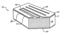
このような空間光変調器の一例は図1に示すような反射型変形可能格子光変調器10である(例えば、特許文献1参照)。この変調器10は、反射表面部を有し、基板16の上部に突出する複数の一定間隔で離隔する変形可能反射型リボン18を含む。この変調器10の製造において、絶縁層11がシリコン基板16上に蒸着される。ついで、犠牲二酸化シリコン膜12および低応力窒化シリコン膜14の蒸着が行われる。窒化物膜14はリボン18の形態にパターニングされ、二酸化シリコン層12の一部がエッチングされることにより、リボン18が窒化物フレーム20により酸化物スペーサ層12上に維持される。単一波長λの光を変調させるため、変調器は、リボン18の厚さと酸化物スペーサ12の厚さがλ/4となるように、設計される。
An example of such a spatial light modulator is a reflective deformable
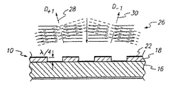
リボン18上の反射表面22と基板16の反射表面間の垂直距離dにより決められる変調器10の格子振幅は、リボン18(第1電極としての役割をするリボン18の反射表面22)と基板16(第2電極としての役割をする基板16の下部伝導膜24との間に電圧を印加することにより制御される。変形されていない状態で、すなわち、何の電圧も印加されていない状態で、格子振幅はλ/2となり、リボンと基板から反射された光間の全体経路差はλとなるので、このような反射光の位相を補強させる。したがって、変形されていない状態で、変調器10は平面ミラーとして光を反射する。変形されていない状態での入射光と反射光を図2に20で示す。
The grating amplitude of the
適正電圧がリボンと基板16間に印加されるとき、静電気力がリボン18を基板16の表面方向に下方に変形させて、格子振幅がλ/4となる。全体経路差は波長の1/2であり、変形されたリボン18から反射された光と基板16から反射された光が干渉する。このような干渉の結果、変調器は入射光26を回折させる。変形された状態が+/−回折モード(D+1、D-1)に回折された光を図3に28と30で示す。
When an appropriate voltage is applied between the ribbon and the
リボン18の下部に空間を形成するのに用いられる湿式工程のうち、かつ変調器10の動作のうち、リボン18と基板16間の付着がこのような装置に大きな問題点であることが判明された。このような付着を減少させるいろいろの方法としては、冷凍乾燥、フォトレジスト−アセトン犠牲層の乾式エッチング、OTS断層処理、リボンの短縮による固いリボンおよび/またはぴんとした窒化物膜の使用、片面または両面を粗くするかまたは屈曲を形成する方法、リボンの下部に反転レールを形成する方法、および表面の化学特性を変化させる方法などがある。1994年6月にスコットランドのヒルトンヘッドアイランドで開催された固状センサおよびアクチュエータに関するワークショップでのサンデヤス等の“高分解能ディスプレイ用変形可能な格子光バルブの表面微細製造”およびアプテ(Apte)等の“高分解能ディスプレイ用格子光バルブ”で、ブリッジの下部に反転レールを形成することで接触領域を減少させ、粗いポリシリコン膜をそれぞれ使用することにより、このような付着を防止することに関して発表した。
Of the wet process used to form the space below the
さらに、アプテ等は、変調器10の機械的動作の特性が印加された電圧の関数としてリボン18の変形でのヒステリシスであることを見つけた。ヒステリシスに対する理論的根拠は、リボン18と基板16間の静電気的引力が変形量の非線形関数である反面、リボン18の硬度と張力による復元力が実質的に線形関数であることによる。図4は、光出力(リボン18の変形量の間接的な表示)が垂直軸上に示され、リボン18と基板16間の電圧が水平軸に示される誘導ヒステリシス特性を示す。したがって、リボン18が基板16と接触する下方への変形の際、これらはその位置にラッチされ、本来印加された電圧より小さい維持電圧を必要とする。
Furthermore, Apte et al. Found that the mechanical behavior characteristic of the
特許文献1は、変調器10に活性素子なしで活性マトリックス設計の利点を提供するラッチング特性を開示する。さらに、特許文献1は、このような特性が使用可能な電力の効率的使用が非常に重要な低電力応用に好ましいことを開示する。しかし、付着問題点において、特許文献1は、接触領域を減少させるように、リボン18の下部に小さなリッジを添加して付着問題を減少させることを開示している。しかし、変調器10の基板が光表面として使用されるため、表面に小さなリッジを追加するための製造工程は、基板16の反射部が高反射率を有するように滑らかでなければならなく、リボン18に平行な平面内に位置しなければならない複雑性を有する。
U.S. Patent No. 6,057,031 discloses a latching characteristic that provides the
通常のディスプレイは、画素の2次元アレイ内で形成される。複数の画素のそれぞれにより形成された不連続イメージは使用者の眼により統合され、全体イメージを表す画素の複合相を形成する。不幸にも、このようなディスプレイ装置の費用は、それぞれの画素が全体アレイを形成するために重複し、それぞれの画素を製造する費用も増加することにより、増加する。このような画素化されたディスプレイの例はテレビジョンまたはコンピュータシステムである。それぞれの画素はLCD装置またはCRTにより形成できる。 A typical display is formed in a two-dimensional array of pixels. The discontinuous images formed by each of the plurality of pixels are integrated by the user's eyes to form a composite phase of pixels representing the entire image. Unfortunately, the cost of such display devices increases because each pixel overlaps to form the entire array and the cost of manufacturing each pixel also increases. An example of such a pixelated display is a television or computer system. Each pixel can be formed by an LCD device or a CRT.
したがって、反射エレメントと基板間の付着を減少させるための複雑な表面処理なしで、このような付着を減少または除去させることが可能な回折格子光バルブが必要である。 Accordingly, there is a need for a grating light valve that can reduce or eliminate such adhesion without complex surface treatments to reduce adhesion between the reflective element and the substrate.
また、イメージ品質の低下なしで、システムを設計するのに必要な画素の数を減少させることにより製造費用を減少させるディスプレイが必要である。 There is also a need for a display that reduces manufacturing costs by reducing the number of pixels required to design a system without degrading image quality.
このような必要性を満足させるための改善された従来技術としては、シリコンライトマシンズ社の特許文献2の“2次元イメージを形成するため、入射光ビームを変調させる方法および装置”がある。 As an improved conventional technique for satisfying such a need, there is "Method and apparatus for modulating an incident light beam to form a two-dimensional image" of Patent Document 2 of Silicon Light Machines.
特許文献2に開示された“2次元イメージを形成するため、入射光ビームを変調させる方法および装置”において、回折格子光バルブは、それぞれ反射表面を有する複数の細長いエレメントを含む。細長いエレメントは、基板上部で互いに平行であり、支持される端部を有し、隣接反射表面の列(GLV(Grating Light Valve)アレイ)を形成するように整列される。細長いエレメントはディスプレイエレメントによって群を形成する。それぞれの群が基板に対して交互に電圧を印加することにより変形される。それぞれの変形された長細いエレメントのほぼ平面の中心部はそれぞれの変形されていないエレメントの中心部から、前もって設定された距離だけ実質的に平行である。前もって設定された距離は変形されていない反射表面と基板間の距離の1/3〜1/4に選択して、長細いエレメントが基板の表面と接触しないようにする。基板との接触を防止することにより、長細いエレメントが基板と付着することを防止する。さらに、前もって設定された距離を制限することで、長細いエレメントを変形させるヒステリシスを防止する。 In “Method and Apparatus for Modulating an Incident Light Beam to Form a Two-Dimensional Image” disclosed in US Pat. No. 6,057,049, the diffraction grating light valve includes a plurality of elongated elements each having a reflective surface. The elongated elements are parallel to each other at the top of the substrate, have supported ends, and are aligned to form a row of adjacent reflective surfaces (GLV (Grating Light Valve) array). The elongate elements form a group by display elements. Each group is deformed by alternately applying a voltage to the substrate. The substantially planar center of each deformed elongated element is substantially parallel to the center of each undeformed element by a preset distance. The pre-set distance is selected to be 1/3 to 1/4 of the distance between the non-deformed reflective surface and the substrate so that the elongate elements do not contact the surface of the substrate. By preventing contact with the substrate, the long and thin elements are prevented from adhering to the substrate. Furthermore, the hysteresis which deform | transforms a long thin element is prevented by restricting the distance set beforehand.
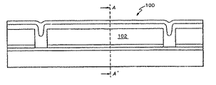
図5は改善された従来技術による変形されていない状態のGLVの長細いエレメント100の側断面図を示す。同図において、長細いエレメント100はその端部により基板(構成層含み)の表面上に突出する。図面で、図面符号102はエアスペースを示す。
FIG. 5 shows a cross-sectional side view of an elongated
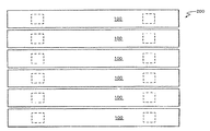
図6は6本の長細いエレメント100を含むGLVお部分平面図を示す。同図に示すように、細長いエレメント100は同じ幅を有し、互いに平行に配置される。細長いエレメント100は小さい隙間を置いて互いに離隔される。したがって、それぞれの長細いエレメント100がほかのエレメントに対して選択的に変形できるようにする。図6に示す六つの長細いエレメント100は、好ましくは単一ディスプレイエレメント200に相当する。したがって、1920本の長細いエレメントの列は、列内に配置された320のディスプレイを有するGLVアレイに相当する。
FIG. 6 shows a partial plan view of the GLV including six
図7は図5の線A−Aについて取った図面で、変形されていない長細いエレメント100を有するディスプレイエレメント100の断面図である。変形されていない状態は、導電体層106に対し、それぞれの長細いエレメント100上のバイアスをイコライジングすることにより、選択される。長細いエレメント100の反射表面が実質的に同一平面上にあるため、長細いエレメント100に入射する光は反射される。
FIG. 7 is a cross-sectional view of the
図8はGLVの変形された長細いエレメント100の側断面図を示す。図8は、変形された状態で、長細いエレメント100が長細いエレメント100の下部の後続層表面と接触せずに突出した状態を維持するものを示す。これは図1〜図3の従来の変調器とは対照される。細長いエレメント100と基板表面間の接触を防止することにより、従来技術の変調器に関連した問題点が防止される。しかし、変形された状態で、長細いエレメント100は垂れる傾向がある。これは、長細いエレメント100がその長手方向に沿って一様に、長手方向に垂直な基板側への静電気引力を受け、反面長細いエレメント100の張力は長細いエレメント100の長手方向に受けるからである。したがって、長細いエレメントの反射表面は平面形でなく曲線形である。
FIG. 8 shows a side cross-sectional view of a modified GLV
しかし、細長いエレメント100の中心部はほぼ平面状態を維持して、それぞれの細長いエレメント100の中心部によってのみ得られた回折光のコントラスト比が満足な値となるようにする。実際に、ほぼ平面の中心部102はポストホール110間の距離の1/3である。したがって、ポストホール75間の距離が75ミクロンであるとき、ほぼ平面の中心部102の長さはおよそ25ミクロンである。
However, the central portion of the
図9は変形された細長いエレメント100が交互に配置されたディスプレイエレメント200の正面図を示す。図9は図8の線B−B′についての断面図である。実質的に除去されていない細長いリボン100が、印加されたバイアス電圧により所望位置に維持される。移動する細長いリボン100の変形状態は、導電体層106に対し長細いエレメント100に交互に駆動電圧を印加することにより達成される。垂直距離d1は、たいてい平面が中心部102(図8参照)に対して一定であり、これによりGLVの格子振幅を限定する。格子振幅d1は駆動される細長いエレメント100上の駆動電圧を調整することで調整可能である。これは、最適のコントラスト比でGLVの精密なチューニングを可能にする。
FIG. 9 shows a front view of a
単一波長(λ1)を有する回折入射光に対し、GLVはディスプレイされるイメージでの最大コントラスト比のため、入射光波長の1/4(λ/4)と同一格子振幅d1を有することが好ましい。しかし、格子振幅d1は、波長λ1の1/2と波長λ1の全体数の合(すなわち、d1=λ1/4、3λ1/4、5λ1/4、・・・、Nλ1/2+λ1/4)と同一の一周距離のみを必要とする。
For diffracted incident light having a single wavelength (λ 1 ), the GLV has the same grating amplitude d 1 as ¼ (λ / 4) of the incident light wavelength for maximum contrast ratio in the displayed image. Is preferred. However, the grating amplitude d 1 is the total number of case half the wavelength lambda 1 of the
図9を参照すると、それぞれの長細いエレメント100の下部表面が距離d2だけ基板から分離されていることが分かる。したがって、長細いエレメント100はGLVの動作のうちに基板と接触しない。これは、反射リボンと基板間での従来技術の変調器の付着に関連した問題点を防止する。
Referring to Figure 9, it can be seen that is separated from the substrate bottom surface of each
図4に示す履歴曲線を参照すると、細長いエレメント100を基板表面に対して1/3ないし1/4の距離で移動させることで入射光を回折させるため、ヒステリシスが防止される。
Referring to the hysteresis curve shown in FIG. 4, the incident light is diffracted by moving the
しかし、シリコンライトマシンズ社製の光変調器は、マイクロミラーの位置制御のため、静電気方式を用いるが、この場合、動作電圧が比較的高く(通常30V程度)印加電圧と変位の関係が線形的でないなどの欠点があるため、結果として光調節の信頼性が高くないという欠点がある。 However, the light modulator manufactured by Silicon Light Machines uses an electrostatic method for controlling the position of the micromirror. In this case, the operating voltage is relatively high (usually about 30 V), and the relationship between the applied voltage and the displacement is linear. As a result, there is a drawback that the reliability of light adjustment is not high.
したがって、本発明は前記のような問題点を解決するためになされたもので、従来の静電駆動方式の反射回折型光変調器の構成とは異なり、圧電駆動方式でマイクロミラーを駆動することにより、変位、駆動速度、信頼性、線形性、および低電圧駆動確保に優れた回折型薄膜圧電マイクロミラーおよびその製造方法を提供することにその目的がある。 Accordingly, the present invention has been made to solve the above-described problems. Unlike the conventional electrostatic drive type reflection diffraction type optical modulator, the present invention drives a micromirror by a piezoelectric drive method. Accordingly, it is an object to provide a diffractive thin film piezoelectric micromirror having excellent displacement, driving speed, reliability, linearity, and low voltage driving, and a method for manufacturing the same.
また、本発明のほかの目的は、薄膜圧電駆動方式でマイクロミラーを駆動して、シリコンウェーハ上の多様な構造設計を可能にする回折型薄膜圧電マイクロミラーおよびその製造方法を提供することにある。 Another object of the present invention is to provide a diffractive thin-film piezoelectric micromirror that enables various structural designs on a silicon wafer by driving the micromirror using a thin-film piezoelectric drive method, and a method for manufacturing the same. .
前記のような目的を達成するため、本発明は、中央部にエアスペースを提供するための陥没部が形成されたシリコン基板と、リボン形状を取っており、中央部が前記基板の陥没部から離隔するように、両端の下面がそれぞれ前記基板の陥没部を外れた両側に付着され、薄膜の圧電材料層を含み、前記圧電材料層に電圧が印加されると、前記陥没部から離隔した部分が上下に駆動され、入射ビームを回折させる圧電ミラー層とを含んでなる回折型薄膜圧電マイクロミラーを提供する。 In order to achieve the above-described object, the present invention has a silicon substrate in which a depressed portion for providing an air space is formed in the central portion and a ribbon shape, and the central portion is formed from the depressed portion of the substrate. The lower surfaces of both ends are attached to the opposite sides of the substrate so as to be separated from each other, include a thin film piezoelectric material layer, and when a voltage is applied to the piezoelectric material layer, a portion separated from the depressed portion A diffractive thin-film piezoelectric micromirror including a piezoelectric mirror layer that is driven up and down to diffract an incident beam.
また、前記目的を達成するため、本発明は、中央部にエアスペースを提供するための陥没部が形成された基板と、リボン形状を取っており、中央部が前記基板の陥没部から離隔するように、両端の下面がそれぞれ前記基板の陥没部を外れた両側に付着され、前記基板の陥没部から離隔した部分が上下に移動可能な下側支持部と、両端が前記基板の陥没部上に位置するように前記下側支持部に積層され、薄膜の圧電材料層を含み、前記圧電材料層の両側に電圧が印加されると、前記陥没部から離隔した部分が上下に駆動され、入射ビームを回折させる圧電ミラー層とを含んでなる回折型薄膜圧電マイクロミラーを提供する。 In order to achieve the above-mentioned object, the present invention has a ribbon shape and a substrate in which a depressed portion for providing an air space in the central portion is formed, and the central portion is separated from the depressed portion of the substrate. As described above, the lower surfaces of both ends are attached to both sides of the substrate, and the lower part of the substrate is movable up and down, and both ends are above the substrate recess. When the voltage is applied to both sides of the piezoelectric material layer, the portion separated from the depressed portion is driven up and down to be incident. Provided is a diffractive thin film piezoelectric micromirror comprising a piezoelectric mirror layer for diffracting a beam.
また、前記目的を達成するため、本発明は、中央部にエアスペースを提供するための陥没部が形成された基板と、リボン形状を取っており、中央部が前記基板の陥没部から離隔するように、両端の下面がそれぞれ前記基板の陥没部を外れた両側に付着された下側支持部と、一端が前記下側支持部の一端に位置し、他端が前記下側支持部の中央部から一端側に所定距離だけ離隔して位置し、薄膜の圧電材料層を含み、前記圧電材料層に電圧が印加されると、収縮および膨張により上下に駆動力を提供する第1圧電層と、一端が前記下側支持部の他端に位置し、他端が前記下側支持部の中央部から他端側に所定距離だけ離隔して位置し、薄膜の圧電材料層を含み、前記圧電材料層に電圧が印加されると、収縮および膨張により上下に駆動力を提供する第2圧電層と、前記下側支持部の中央部に位置し、入射ビームを回折させるためのマイクロミラー層とを含んでなる回折型薄膜圧電マイクロミラーを提供する。 In order to achieve the above-mentioned object, the present invention has a ribbon shape and a substrate in which a depressed portion for providing an air space in the central portion is formed, and the central portion is separated from the depressed portion of the substrate. The lower support part is attached to both sides of the lower surface of the substrate, and one end is positioned at one end of the lower support part, and the other end is the center of the lower support part. A first piezoelectric layer that is positioned at a predetermined distance from the first portion and includes a thin film piezoelectric material layer, and provides a driving force up and down by contraction and expansion when a voltage is applied to the piezoelectric material layer; One end is located at the other end of the lower support portion, the other end is located a predetermined distance away from the center portion of the lower support portion, and includes a thin film piezoelectric material layer, When voltage is applied to the material layer, it provides driving force up and down due to contraction and expansion A second piezoelectric layer that is located on the central portion of the lower support portion provides a diffractive thin-film piezoelectric micromirror comprising a micromirror layer for diffracting the incident beam.
また、前記目的を達成するため、本発明は、絶縁層が表面に形成されたシリコン基板と、リボン形状を取っており、中央部が前記シリコン基板上に所定距離だけ立ち上がり、両端の下面がそれぞれ前記シリコン基板に付着され、前記シリコン基板から所定距離だけ離隔した部分が上下に移動可能な下側支持部と、前記下側支持部に積層され、薄膜の圧電材料層を含み、前記圧電材料層の両側に電圧が印加されると、収縮および膨張による上下駆動力を発生させて、前記シリコン基板から所定距離だけ離隔した中央部を上下に駆動させ、入射ビームを回折させるための圧電ミラー層とを含んでなる回折型薄膜圧電マイクロミラーを提供する。 Further, in order to achieve the above object, the present invention has a silicon substrate with an insulating layer formed on the surface and a ribbon shape, the central portion rises on the silicon substrate by a predetermined distance, and the lower surfaces at both ends are respectively A portion attached to the silicon substrate and spaced apart from the silicon substrate by a predetermined distance includes a lower support portion that can move up and down, and a thin film piezoelectric material layer that is laminated on the lower support portion, the piezoelectric material layer A piezoelectric mirror layer for diffracting an incident beam by generating a vertical driving force due to contraction and expansion, driving a central part spaced apart from the silicon substrate by a predetermined distance up and down. A diffractive thin-film piezoelectric micromirror comprising:
また、前記目的を達成するため、本発明は、絶縁層が表面に形成された基板と、リボン形状を取っており、中央部が前記基板から立ち上がり、両端の下面がそれぞれ前記基板の両側に付着され、前記基板から立ち上がった部分が上下移動可能な下側支持部と、一端が前記下側支持部の一端に位置し、他端が前記下側支持部の中央部から一端側に所定距離だけ離隔して位置し、薄膜の圧電材料層を含み、前記圧電材料層に電圧が印加されると、収縮および膨張により上下に駆動力を提供する第1圧電層と、一端が前記下側支持部の他端に位置し、他端が前記下側支持部の中央部から他端側に所定距離だけ離隔して位置し、薄膜の圧電材料層を含み、前記圧電材料層に電圧が印加されると、収縮および膨張により上下に駆動力を提供する第2圧電層と、前記下側支持部の中央部に位置し、入射ビームを回折させるためのマイクロミラー層とを含んでなる回折型薄膜圧電マイクロミラーを提供する。 In order to achieve the above object, the present invention has a substrate having an insulating layer formed on the surface and a ribbon shape, a central portion rises from the substrate, and lower surfaces of both ends are attached to both sides of the substrate. A lower support portion that is vertically movable at a portion rising from the substrate, and one end is positioned at one end of the lower support portion, and the other end is a predetermined distance from the central portion of the lower support portion to one end side. A first piezoelectric layer that is spaced apart and includes a thin film piezoelectric material layer, and provides a driving force up and down by contraction and expansion when a voltage is applied to the piezoelectric material layer, and one end of the lower support portion The other end of the lower support portion is located a predetermined distance away from the central portion of the lower support portion and includes a thin film piezoelectric material layer, and a voltage is applied to the piezoelectric material layer. And a second piezoelectric element that provides driving force up and down by contraction and expansion When located in central part of the lower support portion provides a diffractive thin-film piezoelectric micromirror comprising a micromirror layer for diffracting the incident beam.
また、前記目的を達成するため、本発明は、シリコンウェーハ上にマスク層を形成し、パターニングを行って陥没部を形成する第1段階と、前記第1段階で形成された陥没部を埋め込むように犠牲層を形成する第2段階と、前記陥没部が埋め込まれたシリコンウェーハ上に圧電ミラー層を形成する第3段階と、前記第3段階で形成された圧電ミラー層を、複数のリボン形状の配列となるように、エッチングし、犠牲層を除去することで、回折型薄膜圧電マイクロミラーを形成する第4段階とを含んでなる回折型薄膜マイクロミラーの製造方法を提供する。 According to another aspect of the present invention, a mask layer is formed on a silicon wafer and patterned to form a depressed portion, and the depressed portion formed in the first step is embedded. A second step of forming a sacrificial layer, a third step of forming a piezoelectric mirror layer on the silicon wafer in which the recessed portion is embedded, and the piezoelectric mirror layer formed in the third step are formed into a plurality of ribbon shapes. And a fourth step of forming a diffractive thin film piezoelectric micromirror by etching and removing the sacrificial layer so as to obtain an array of diffractive thin film micromirrors.
また、前記目的を達成するため、本発明は、シリコン基板上にマスク層を形成し、パターニングを行って陥没部を形成する第1段階と、前記第1段階で形成された陥没部を埋め込むように犠牲層を形成する第2段階と、前記陥没部が埋め込まれたシリコン基板上に下側支持部を形成する第3段階と、前記第3段階で形成された下側支持部上に、一端の下面が前記陥没部の外側に位置し、他端の下面が前記陥没部の中央部から外側に所定距離だけ離隔して位置し、互いに対向するように形成された一対の圧電ミラー層を形成する第4段階と、前記下側支持部の中央部にマイクロミラー層を形成する第5段階と、前記一対の圧電ミラー層と下側支持部を、複数のリボン形状の配列となるようにエッチングし、犠牲層を除去することで、回折型薄膜圧電マイクロミラーを形成する第6段階とを含んでなる回折型薄膜マイクロミラーの製造方法を提供する。 According to another aspect of the present invention, a mask layer is formed on a silicon substrate and patterned to form a depressed portion, and the depressed portion formed in the first step is embedded. A second step of forming a sacrificial layer, a third step of forming a lower support portion on the silicon substrate in which the depression is embedded, and a lower support portion formed in the third step. A pair of piezoelectric mirror layers are formed so that the lower surface of each is positioned outside the depressed portion, and the lower surface of the other end is spaced apart from the central portion of the depressed portion by a predetermined distance and facing each other. Etching the fourth stage of forming, a fifth stage of forming a micromirror layer in the center of the lower support part, and the pair of piezoelectric mirror layers and the lower support part in a plurality of ribbon-like arrangements And by removing the sacrificial layer, a diffractive thin film To provide a method for manufacturing a diffractive thin-film micromirror comprising a sixth step of forming a conductive micromirror.
また、前記目的を達成するため、本発明は、シリコン基板上に犠牲層を積層し、マスク層を形成し、エッチングすることで、立ち上がり部を形成する第1段階と、前記第1段階で立ち上がり部が形成されたシリコン基板上に下側支持部を積層する第2段階と、前記第2段階で形成された下側支持部上に圧電ミラー層を形成する第3段階と、前記第3段階で形成された圧電ミラー層を、複数のリボン形状の配列となるように、エッチングし、犠牲層を除去することで、回折型薄膜圧電マイクロミラーを形成する第4段階とを含んでなる回折型薄膜マイクロミラーの製造方法を提供する。
In order to achieve the above object, according to the present invention, a sacrificial layer is stacked on a silicon substrate, a mask layer is formed, and etching is performed to form a rising portion, and the rising portion is formed in the first step. A second stage of laminating a lower support on the silicon substrate on which the portion is formed, a third stage of forming a piezoelectric mirror layer on the lower support formed in the second stage, and the third stage A diffractive type including a fourth step of forming a diffractive thin-film piezoelectric micromirror by etching the piezoelectric mirror layer formed in
また、前記目的を達成するため、本発明は、シリコン基板上に犠牲層を積層し、マスク層を形成し、エッチングすることで、立ち上がり部を形成する第1段階と、前記第1段階で立ち上がり部が形成されたシリコン基板上に下側支持部を積層する第2段階と、前記第2段階で形成された下側支持部上に、一端の下面が前記立ち上がり部の外側に位置し、他端の下面が前記立ち上がり部の中央部から外側に所定距離だけ離隔して位置し、互いに対向するように形成された一対の圧電ミラー層を形成する第3段階と、前記下側支持部の中央部にマイクロミラー層を形成する第4段階と、前記一対の圧電ミラー層と下側支持部を、複数のリボン形状の配列となるようにエッチングし、犠牲層を除去することで、回折型薄膜圧電マイクロミラーを形成する第5段階とを含んでなる回折型薄膜マイクロミラーの製造方法を提供する。 In order to achieve the above object, according to the present invention, a sacrificial layer is stacked on a silicon substrate, a mask layer is formed, and etching is performed to form a rising portion, and the rising portion is formed in the first step. A second stage of laminating the lower support part on the silicon substrate having the part formed thereon, and a lower support part formed in the second stage, the lower surface of one end being positioned outside the rising part, A third step of forming a pair of piezoelectric mirror layers formed so that the lower surface of the end is spaced apart from the central part of the rising part by a predetermined distance and facing each other; and the center of the lower support part A fourth step of forming a micromirror layer on the portion, and etching the pair of piezoelectric mirror layers and the lower support portion so as to form a plurality of ribbon-shaped arrays, and removing the sacrificial layer, thereby diffractive thin film Form piezoelectric micromirror To provide a method for manufacturing a diffractive thin-film micromirror comprising a fifth step that.
以上のような本発明によると、従来技術による静電気方式は非線形的であるに対し、圧電素子を用いると、印加電圧と変位の関係が線形成を有する効果がある。 According to the present invention as described above, the electrostatic method according to the prior art is non-linear, but when a piezoelectric element is used, the relationship between the applied voltage and the displacement has an effect of forming a line.
また、本発明によると、静電気方式に比べ、相対的に低い電圧で同等程度の変位を得ることができ、高い駆動速度を得ることができる効果がある。 Further, according to the present invention, it is possible to obtain the same degree of displacement with a relatively low voltage as compared with the electrostatic method, and there is an effect that a high driving speed can be obtained.
また、本発明によると、信頼性のあるリボン変位の調節を可能にすることで、静電気方式によっては難しかったアナログコントロール(gray scale control)が可能である効果がある。 In addition, according to the present invention, it is possible to perform analog scale control (gray scale control), which is difficult in some electrostatic methods, by enabling reliable adjustment of ribbon displacement.
また、本発明によると、圧電マイクロミラーアレイの構成において、リボンの長さおよび幅に対する多様なデザインが可能であるので、当該アプリケーションで要求される光効率の調節が容易になる効果がある。 Further, according to the present invention, in the configuration of the piezoelectric micromirror array, various designs for the length and width of the ribbon are possible, so that there is an effect that the light efficiency required for the application can be easily adjusted.
以下、図10aないし図17cに基づいて本発明の好ましい一実施例を詳細に説明するとつぎのようである。 Hereinafter, a preferred embodiment of the present invention will be described in detail with reference to FIGS. 10a to 17c.
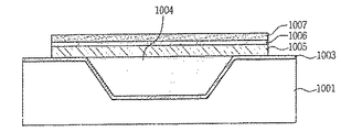
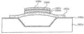
図10a〜10jは本発明の一実施例による陥没部を有する回折型薄膜圧電マイクロミラーの製造過程の側断面図である。 10a to 10j are side cross-sectional views illustrating a manufacturing process of a diffractive thin film piezoelectric micromirror having a depression according to an embodiment of the present invention.
図10aに示すように、シリコンウェーハ1001上に、エッチングを行うため、熱酸化などの方法でマスク層1002を0.1〜1.0μmの厚さに形成し、パターニングを行うことで、シリコンエッチングを準備する。
As shown in FIG. 10a, in order to perform etching on a
図10bに示すように、TMAHまたはKOHなどのシリコンをエッチングし得る溶液でシリコンを適当な厚さにエッチングした後、マスク層1002を除去する。このエッチングにおいては、湿式エッチングだけでなく乾式エッチングも用いることができる。
As shown in FIG. 10b, after etching the silicon to a suitable thickness with a solution that can etch silicon, such as TMAH or KOH, the
図10cに示すように、エッチングされたシリコンに、さらに熱酸化などの方法で絶縁および食刻防止層1003を形成する。
As shown in FIG. 10c, an insulating and
図10dに示すように、シリコンウェーハ1001のエッチング部位に、低圧化学気相蒸着(LPCVD)または化学気相蒸着(PECVD)の方法でポリシリコンまたはアモルファスシリコンなどを蒸着して犠牲層1004を形成した後、平坦にポリシングを行う。この際、SOI(Silicon On Insulator)を使用する場合は、ポリシリコンの蒸着およびポリシングなしでも可能である。
As shown in FIG. 10d, a
その後、Si3N4などのシリコンナイトライド系列をLPCVDまたはPECVD方法で、一例として0.1〜5.0μmの厚さ範囲に蒸着した後、SiO2を熱酸化またはPECVD法で0.1〜5μmの範囲に蒸着するが、必要に応じて省略可能である。 Thereafter, a silicon nitride series such as Si 3 N 4 is deposited by LPCVD or PECVD, for example, in a thickness range of 0.1 to 5.0 μm, and then SiO 2 is 0.1 or less by thermal oxidation or PECVD. Although it vapor-deposits in the range of 5 micrometers, it is omissible as needed.
ついで、図10eに示すように、圧電材料を支持するための下側支持部1005をシリコンウェーハ1001に蒸着し、下側支持部1005を構成する材料としてはSi酸化物(一例として、SiO2)、Si窒化物系列(一例として、Si3N4など)、セラミック基板(Si、ZrO2,Al2O3)、Siカーバイドなどが可能である。このような下側支持部1005は必要に応じて省略できる。
Next, as shown in FIG. 10e, a
図10fに示すように、下側支持部1005上に下部電極1006を形成する。この際、下部電極1006の電極材料としては、Pt、Ta/Pt、Ni、Au、Al、AuO2などが使用でき、0.01〜3μmの範囲でスパッタリングまたは蒸発などの方法で蒸着する。
As shown in FIG. 10 f, the
図10gに示すように、下部電極1006上に、圧電材料1007を湿式法(スクリーンプリンティング、Sol-Gel coatingなど)および乾式法(スパッタリング、蒸発、MOCVD、蒸着など)で0.01〜20.0μmの範囲に形成する。そして、使用される圧電材料1007としては、上下型圧電材料と左右型圧電材料を共に使用することができるが、PZT、PMN−PT、PLZT、AIN、ZnOなどの圧電材料を使用することができ、Pb、Zr、Znまたはチタンなどを少なくとも1種以上含む圧電電解材料を対象とする。
As shown in FIG. 10g, a
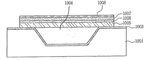
図10hに示すように、圧電材料1007上に上部電極1008を形成する。このときに使用可能な材料としては、Pt、Ta/Pt、Ni、Au、Al、Ti/Pt、IrO2、RuO2などが使用でき、0.01〜3μmの範囲でスパッタリングまたは蒸発などの方法で形成する。
As shown in FIG. 10 h, the
図10iに示すように、上部電極1008上にマイクロミラー1009を付着するが、その材料としては、Ti、Cr、Cu、Ni、Al、Au、Ag、Pt、Au/Crなどの光反射物質が使用される。
As shown in FIG. 10i, a
この際、上部電極1008をマイクロミラーとして使用するか、または別途のマイクロミラーを上部電極1008上に蒸着することができる。
At this time, the
図10jに示すように、このように形成された回折型薄膜圧電マイクロミラーアレイの母体から、回折型薄膜圧電マイクロミラーアレイを形成するためには、フォトレジストなどのマスク層を介してパターニングを行った後、マイクロミラー1009、上部電極1008、圧電材料1007、下部電極1006、下側支持部1005をエッチングすることにより、回折型薄膜圧電マイクロミラーアレイを形成する。その後、犠牲層1004をXeF2ガスでエッチングする。
As shown in FIG. 10j, in order to form a diffractive thin film piezoelectric micromirror array from the base of the diffractive thin film piezoelectric micromirror array thus formed, patterning is performed through a mask layer such as a photoresist. Thereafter, the
ここでは、回折型薄膜圧電マイクロミラーアレイの母体から回折型薄膜圧電マイクロミラーアレイを形成した後、犠牲層1004を除去する過程を説明したが、犠牲層1004を除去した後、マイクロミラーアレイを形成することもできる。
Here, the process of removing the
すなわち、まず回折型薄膜圧電マイクロミラーアレイの母体の、下側支持部1005の形成されていない区間にホールを形成し、犠牲層1004をXeF2ガスでエッチングした後、回折型薄膜圧電マイクロミラーアレイの母体にフォトレジストなどのマスク層を介してパターニングを行った後、マイクロミラー1009、上部電極1008、圧電材料1007、下部電極1006、下側支持部1005をエッチングしてマイクロミラーアレイを形成する。
That is, first, holes are formed in a section of the base of the diffractive thin film piezoelectric micromirror array where the
図11a〜11cは変形されていない圧電材料を持っている多様な形態の陥没部を有する回折型薄膜圧電マイクロミラーの側断面図である。 11a to 11c are cross-sectional side views of diffractive thin-film piezoelectric micromirrors having various forms of depressions having undeformed piezoelectric material.
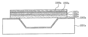
図11aはシリコンウェーハの犠牲層がエアスペースで取り替えられているものを示す。したがって、圧電材料は、その端部により基板の表面上に懸架される。そして、下部電極層1006a、圧電材料層1007a、上部電極層1008a、マイクロミラー1009aは下側支持部1005a上に位置していることが分かる。
FIG. 11a shows the sacrificial layer of the silicon wafer being replaced by an air space. Thus, the piezoelectric material is suspended on the surface of the substrate by its ends. It can be seen that the
図11bはシリコンウェーハの犠牲層がエアスペースで取り替えられているものを示す。したがって、圧電材料は、その端部により基板の表面上に懸架される。ここで、マイクロミラー1009bは下側支持部1005bの中央に位置していることが分かる。また、下部電極層1006b、圧電材料層1007b、上部電極層1008bは下側支持部1005bの両側に位置していることが分かる。このような形態の回折型薄膜圧電マイクロミラーを形成するためには、上部電極層1008bまで形成した後、中央部の下部電極層1006b、圧電材料層1007b、上部電極層1008bをエッチングした後、エッチングされた中央部にマイクロミラー1009bを形成する。
FIG. 11b shows the sacrificial layer of the silicon wafer being replaced with an air space. Thus, the piezoelectric material is suspended on the surface of the substrate by its ends. Here, it can be seen that the micromirror 1009b is located at the center of the
図11cはシリコンウェーハの犠牲層がエアスペースで取り替えられているものを示す。したがって、圧電材料は、その端部により基板の表面上に懸架される。ここで、下部電極層1006c、圧電材料層1007c、上部電極層1008c、マイクロミラー1009cは下側支持部1005c上に位置していることが分かる。
FIG. 11c shows the sacrificial layer of the silicon wafer being replaced with an air space. Thus, the piezoelectric material is suspended on the surface of the substrate by its ends. Here, it can be seen that the
図12a〜図12cは変形された後の圧電材料を持っている多様な形態の陥没部を有する回折型薄膜圧電マイクロミラーの側断面図である。 12a to 12c are cross-sectional side views of diffractive thin-film piezoelectric micromirrors having various types of depressions having a deformed piezoelectric material.
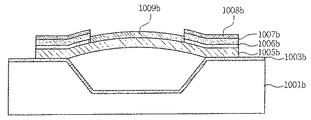
図12aは、圧電材料1007aの上下に電圧が印加されることにより、圧電材料の収縮力および膨張力により、下側支持部1005a、下部電極層1006a、圧電材料層1007a、上部電極層1008a、マイクロミラー1009aが下方に垂れている上体を示す。この際、圧電材料1007aは左右に収縮して左右方向への力を発生させるが、下側支持部1005aに圧電材料1007aの下部が堅く固着されているため、左右方向に作用する力は究極に圧電材料1007aを下方に引き下げる。
FIG. 12a shows that a
図12bは、下側支持部1005bの両側に位置する圧電材料層1007bの上下に電圧が印加されることにより、左右方向に収縮する力が発生することが分かる。この際、圧電材料1007bは左右に収縮して左右方向への力を発生させるが、下側支持部1005bに圧電材料1007bの下部が堅く固着されているため、左右方向に作用する力は究極に圧電材料1007bを上方に引き上げることになる。その結果、下側支持部1005bは上方に膨らみ、下側支持部1005bの中央に位置するマイクロミラー1009bは上方に膨らむ。
FIG. 12B shows that a force contracting in the left-right direction is generated by applying a voltage to the upper and lower sides of the
図12cは下側支持部1005cの中央に位置する圧電材料1007cの上下に電圧が印加されると、下部電極層1006c、圧電材料層1007c、上部電極層1008c、マイクロミラー1009cが上方に立ち上がることが分かる。
In FIG. 12c, when a voltage is applied above and below the
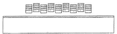
図13aは陥没部を有する回折型薄膜圧電マイクロミラーが同一幅で配置されたディスプレイエレメントの駆動例を示す側断面図である。回折型薄膜圧電マイクロミラーは電圧の印加により上下に移動する。 FIG. 13A is a side sectional view showing a driving example of a display element in which diffractive thin film piezoelectric micromirrors having depressions are arranged with the same width. The diffractive thin film piezoelectric micromirror moves up and down by applying a voltage.
図13bは陥没部を有する回折型薄膜圧電マイクロミラーが相違した幅で交互に配置されたディスプレイエレメントの駆動例を示す側断面図である。回折型薄膜圧電マイクロミラーは電圧の印加により上下に移動する。 FIG. 13B is a side sectional view showing an example of driving display elements in which diffractive thin film piezoelectric micromirrors having depressions are alternately arranged with different widths. The diffractive thin film piezoelectric micromirror moves up and down by applying a voltage.
図13cは陥没部を有する回折型薄膜圧電マイクロミラーが同一間隔で配置されたディスプレイエレメントの駆動例を示す側断面図である。ここで、絶縁層の上面にマイクロミラーが全面に形成されて、入射光を回折させる。 FIG. 13c is a side sectional view showing a driving example of a display element in which diffractive thin film piezoelectric micromirrors having depressions are arranged at the same interval. Here, a micromirror is formed on the entire top surface of the insulating layer to diffract incident light.
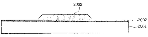
図14a〜図14hは本発明のほかの実施例による立ち上がり部を有する薄膜圧電光変調器の製造過程を示す側断面図である。 14a to 14h are side cross-sectional views illustrating a manufacturing process of a thin film piezoelectric light modulator having a rising portion according to another embodiment of the present invention.
図14aに示すように、シリコンに、熱酸化などの方法で絶縁および食刻防止層2002を形成する。すなわち、シリコンウェーハの表面に、SiO2などで絶縁および食刻防止層2002を形成する。
As shown in FIG. 14a, an insulating and
そして、エアスペースを形成するため、シリコンウェーハ2001の絶縁および食刻防止層2002の上面に、LPCVDまたはPECVDの方法でポリシリコンまたはアモルファスシリコンなどを蒸着した後、平坦にポリシングを行って、犠牲層2003を形成する。
Then, in order to form an air space, polysilicon or amorphous silicon or the like is deposited on the upper surface of the insulating and
その後、犠牲層2003上に、エッチングのため、熱酸化などの方法でマスク層2004を0.1〜3.0μmの厚さに形成し、パターニングを行うことで、シリコンエッチングを準備する。
Thereafter, on the
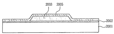
図14bに示すように、TMAHまたはKOHなどのシリコンをエッチングし得る溶液でシリコンを適当な厚さにエッチングした後、マスク層2004を除去する。
As shown in FIG. 14b, the
Si3N4などのシリコンナイトライド系列をLPCVDまたはPECVD方法で、一例として0.1〜5.0μmの厚さ範囲に蒸着した後、SiO2を熱酸化またはPECVD法で0.1〜3μmの範囲に蒸着するが、必要に応じて省略可能である。 A silicon nitride series such as Si 3 N 4 is deposited by LPCVD or PECVD in an example thickness range of 0.1 to 5.0 μm, and then SiO 2 is thermally oxidized or PECVD by 0.1 to 3 μm. Vapor deposition is possible, but can be omitted if necessary.
ついで、図14cに示すように、圧電材料を支持するための下側支持部2005を絶縁および食刻防止層2002および犠牲層2003上に蒸着し、下側支持部2005を構成する材料としては、Si酸化物(一例として、SiO2)、Si窒化物系列(一例として、Si3N4など)、セラミック基板(一例として、Si、ZrO2、Al2O3)、シリコンカーバイドなどが可能である。このような下側支持部2005は必要に応じて省略可能である。
Next, as shown in FIG. 14c, a
図14dに示すように、下側支持部2005上に下部電極2006を形成する。この際、下部電極2006の電極材料としては、Pt、Ta/Pt、Ni、Au、Al、AuO2などが使用でき、0.01〜3μmの範囲でスパッタリングまたは蒸発などの方法で蒸着する。
As shown in FIG. 14 d, the
図14eに示すように、下部電極2006上に、圧電材料2007を湿式法(スクリーンプリンティング、Sol-Gel coatingなど)および乾式法(スパッタリング、蒸発、蒸着など)で0.01〜20.0μmの範囲に形成する。そして、使用される圧電材料2007としては、上下圧電材料と左右圧電材料を全て使用することができるが、PZT、PMN−PT、PLZT、A IN、ZnOなどの圧電材料を使用することができ、Pb、Zr、Znまたはチタンなどを少なくとも1種以上含む圧電電解材料を対象とする。
As shown in FIG. 14e, the
図14fに示すように、圧電材料2007上に上部電極2008を形成する。このときに使用可能な材料としては、Pt、Ta/Pt、Ni、Au、Al、Ti/Pt、IrO2、RuO2などが使用でき、0.01〜3μmの範囲でスパッタリングまたは蒸発などの方法で形成する。
As shown in FIG. 14 f, the
図14gに示すように、上部電極2008上にマイクロミラー2009を付着するが、その材料としては、Ti、Cr、Cu、Ni、Al、Au、Ag、Pt、Au/Crなどの光反射物質が使用される。
As shown in FIG. 14g, the
この際、上部電極2008をマイクロミラーとして使用するか、または別途のマイクロミラーを上部電極2008上に蒸着することができる。
At this time, the
図14hに示すように、このように形成された回折型薄膜圧電マイクロミラーアレイの母体から、回折型薄膜圧電マイクロミラーアレイを形成するためには、フォトレジストなどのマスク層を介してパターニングを行った後、マイクロミラー2009、上部電極2008、圧電材料2007、下部電極2006、下側支持部2005をエッチングすることにより、回折型薄膜圧電マイクロミラーアレイを形成する。その後、犠牲層2003をXeF2ガスでエッチングする。
As shown in FIG. 14h, in order to form a diffractive thin film piezoelectric micromirror array from the base of the diffractive thin film piezoelectric micromirror array thus formed, patterning is performed through a mask layer such as a photoresist. Thereafter, the
ここでは、回折型薄膜圧電マイクロミラーアレイの母体から回折型薄膜圧電マイクロミラーアレイを形成した後、犠牲層2003を除去する過程を説明したが、犠牲層2003を除去した後、マイクロミラーアレイを形成することもできる。
Here, the process of removing the
すなわち、まず回折型薄膜圧電マイクロミラーアレイの母体の、下側支持部2005の形成されていない区間にホールを形成し、犠牲層2003をXeF2ガスでエッチングした後、回折型薄膜圧電マイクロミラーアレイの母体にフォトレジストなどのマスク層を介してパターニングを行った後、マイクロミラー2009、上部電極2008、圧電材料2007、下部電極2006、下側支持部2005をエッチングしてマイクロミラーアレイを形成する。
That is, first, a hole is formed in a section of the base of the diffractive thin film piezoelectric micromirror array where the
図15a〜15cは変形されていない圧電材料を持っている多様な形態の立ち上がり部を有する回折型薄膜圧電マイクロミラーの側断面図である。 15a to 15c are cross-sectional side views of diffractive thin film piezoelectric micromirrors having various forms of rising portions having undeformed piezoelectric materials.
図15aはシリコンウェーハの犠牲層がエアスペースで取り替えられているものを示す。したがって、圧電材料は、その端部により基板の表面上に立ち上がる。そして、下部電極層2006a、圧電材料層2007a、上部電極層2008a、マイクロミラー2009aは下側支持部2005a上に位置していることが分かる。図11aと異なる点は、圧電材料が絶縁および食刻防止層上に立ち上がっていることである。
FIG. 15a shows the sacrificial layer of the silicon wafer being replaced by an air space. Therefore, the piezoelectric material rises on the surface of the substrate by the end portion. It can be seen that the
図15bはシリコンウェーハの犠牲層がエアスペースで取り替えられているものを示す。したがって、圧電材料は、その端部により基板の表面上に立ち上がる。ここで、マイクロミラー2009bは下側支持部2005bの中央に位置していることが分かる。また、下部電極層2006b、圧電材料層2007b、上部電極層2008bは下側支持部2005bの両側に位置していることが分かる。このような形態の回折型薄膜圧電マイクロミラーを形成するためには、上部電極層2008bまで形成した後、中央部の下部電極層2006b、圧電材料層2007b、上部電極層2008bをエッチングした後、エッチングされた中央部にマイクロミラー2009bを形成する。図11bと異なる点は圧電材料が絶縁および食刻防止層上に立ち上がっていることである。
FIG. 15b shows the sacrificial layer of the silicon wafer being replaced by an air space. Therefore, the piezoelectric material rises on the surface of the substrate by the end portion. Here, it can be seen that the
図15cはシリコンウェーハの犠牲層がエアスペースで取り替えられているものを示す。したがって、圧電材料は、その端部により基板の表面上に立ち上がる。ここで、下部電極層2006c、圧電材料層2007c、上部電極層2008c、マイクロミラー2009cは下側支持部2005c上に位置していることが分かる。図11cと異なる点は、圧電材料が絶縁および食刻防止層上に立ち上がっていることである。
FIG. 15c shows the sacrificial layer of the silicon wafer being replaced with an air space. Therefore, the piezoelectric material rises on the surface of the substrate by the end portion. Here, it can be seen that the
図16a〜図16cは変形された後の圧電材料を持っている多様な形態の立ち上がり部を有する回折型薄膜圧電マイクロミラーの側断面図である。 16a to 16c are cross-sectional side views of diffractive thin film piezoelectric micromirrors having various forms of rising portions having the piezoelectric material after being deformed.
図16aは、圧電材料2007aの上下に電圧が印加されることにより、圧電材料の収縮力および膨張力により、下側支持部2005a、下部電極層2006a、圧電材料層1007a、上部電極層2008a、マイクロミラー2009aが下方に垂れている状態を示す。この際、圧電材料2007aは左右に収縮して左右方向への力を発生させるが、下側支持部2005aに圧電材料2007aの下部が堅く固着されているため、左右方向に作用する力は究極に圧電材料2007aを下方に引き下げる。
FIG. 16a shows that when a voltage is applied to the top and bottom of the
図16bは、下側支持部2005bの両側に位置する圧電材料層2007bの上下に電圧が印加されることにより、左右方向に収縮する力が発生することが分かる。この際、圧電材料2007bは左右に収縮して左右方向への力を発生させるが、下側支持部2005bに圧電材料2007bの下部が堅く固着されているため、左右方向に作用する力は究極に圧電材料2007bを上方に引き上げることになる。その結果、下側支持部2005bは上方に膨らみ、下側支持部2005cの中央に位置するマイクロミラー2009bは上方に膨らむ。
FIG. 16b shows that a force contracting in the left-right direction is generated by applying a voltage to the upper and lower sides of the
図16cは下側支持部2005cの中央に位置する圧電材料2007cの上下に電圧が印加されると、下部電極層2006c、圧電材料層2007c、上部電極層2008c、マイクロミラー2009cが上方に膨らむことが分かる。
In FIG. 16c, when a voltage is applied above and below the
図17aは立ち上がり部を有する回折型薄膜圧電マイクロミラーが同一幅で配置されたディスプレイエレメントの駆動例を示す側断面図である。回折型薄膜圧電マイクロミラーは電圧の印加により上下に移動する。 FIG. 17A is a side sectional view showing an example of driving a display element in which diffractive thin film piezoelectric micromirrors having rising portions are arranged with the same width. The diffractive thin film piezoelectric micromirror moves up and down by applying a voltage.
図17bは立ち上がり部を有する回折型薄膜圧電マイクロミラーが相違した幅で交互に配置されたディスプレイエレメントの駆動例を示す側断面図である。回折型薄膜圧電マイクロミラーは電圧の印加により上下に移動する。 FIG. 17B is a sectional side view showing an example of driving display elements in which diffractive thin film piezoelectric micromirrors having rising portions are alternately arranged with different widths. The diffractive thin film piezoelectric micromirror moves up and down by applying a voltage.
図17cは立ち上がり部を有する回折型薄膜圧電マイクロミラーが同一間隔配置されたディスプレイエレメントの駆動例を示す側断面図である。ここで、絶縁層の上面にマイクロミラーが上面に形成され、形成されたマイクロミラーは入射光を回折させる。 FIG. 17c is a side sectional view showing a driving example of a display element in which diffractive thin film piezoelectric micromirrors having rising portions are arranged at the same interval. Here, a micromirror is formed on the upper surface of the insulating layer, and the formed micromirror diffracts incident light.
本発明においては、圧電材料層が単層の場合について説明したが、低電圧駆動のため、圧電材料層を多層に構成することができる。この際、下部電極層と上部電極層も多層に構成される。 In the present invention, the case where the piezoelectric material layer is a single layer has been described, but the piezoelectric material layer can be formed in multiple layers for low voltage driving. At this time, the lower electrode layer and the upper electrode layer are also formed in multiple layers.
すなわち、下から第1下部電極層、第1圧電材料層、第1上部電極層、および第2下部電極層、第2圧電材料層、第2上部電極層、および第3下部電極層、・・・などに構成可能である。 That is, from the bottom, the first lower electrode layer, the first piezoelectric material layer, the first upper electrode layer, and the second lower electrode layer, the second piezoelectric material layer, the second upper electrode layer, and the third lower electrode layer,・ It can be configured.
以上説明した本発明による回折型薄膜圧電マイクロミラーおよびその製造方法を実施するための一実施例に過ぎないもので、本発明は前記実施例に限定されなく、特許請求の範囲に記載された本発明の範囲から逸脱することなく、本発明が属する分野の通常の知識を持った者であればだれでも本発明を多様に変更実施することができる。 It is only one example for carrying out the diffractive thin-film piezoelectric micromirror and the manufacturing method thereof according to the present invention described above. The present invention is not limited to the above-described example, and the present invention described in the claims. Without departing from the scope of the invention, anyone having ordinary knowledge in the field to which the present invention belongs can make various modifications of the present invention.
1001、2001 シリコンウェーハ
1002、2004 マスク層
1003 絶縁および食刻防止層
1004、2003 犠牲層
1005,005 下側支持部
1006、2006 下部電極
1007、2007 圧電材料
1008、2008 上部電極
1009、2009 マイクロミラー
1001, 2001
Claims (24)
リボン形状を取っており、中央部が前記基板の陥没部から離隔するように、両端の下面がそれぞれ前記基板の陥没部を外れた両側に付着され、薄膜の圧電材料層を含み、前記薄膜の圧電材料層に電圧が印加されると、前記陥没部から離隔した部分が上下に駆動され、入射ビームを回折させる圧電ミラー層とを含んでなることを特徴とする回折型薄膜圧電マイクロミラー。 A substrate on which a depressed portion for providing an air space in the center is formed;
It has a ribbon shape, and the lower surface of both ends are attached to both sides of the substrate from the depressed portion so that the central portion is separated from the depressed portion of the substrate, and includes a thin film piezoelectric material layer, A diffractive thin-film piezoelectric micromirror, comprising: a piezoelectric mirror layer that diffracts an incident beam when a voltage is applied to the piezoelectric material layer, and a portion separated from the depression is driven up and down.
リボン形状を取っており、中央部が前記基板の陥没部から離隔するように、両端の下面がそれぞれ前記基板の陥没部を外れた両側に位置し、圧電電圧を提供するための下部電極層と、
前記下部電極層上に積層され、両面に電圧が印加されると、収縮および膨張して上下に駆動力を発生させる圧電材料層と、
前記圧電材料層上に積層され、前記圧電材料層に圧電電圧を提供し、入射ビームを回折させるための上部電極およびミラー層とを含むことを特徴とする請求項1記載の回折型薄膜圧電マイクロミラー。 The piezoelectric mirror layer is
A bottom electrode layer for providing a piezoelectric voltage, wherein the bottom surface of each end is located on both sides of the substrate, so that the central portion is separated from the recess of the substrate, ,
A piezoelectric material layer that is laminated on the lower electrode layer and contracts and expands when a voltage is applied to both sides thereof to generate a driving force up and down;
The diffractive thin-film piezoelectric micro of claim 1, further comprising an upper electrode and a mirror layer stacked on the piezoelectric material layer, providing a piezoelectric voltage to the piezoelectric material layer, and diffracting an incident beam. mirror.
リボン形状を取っており、中央部が前記基板の陥没部から離隔するように、両端の下面がそれぞれ前記基板の陥没部を外れた両側に位置し、圧電電圧を提供するための第1電極層と、
前記第1電極層上に多層に積層され、各層に電圧が印加されると、電圧が印加された層が収縮および膨張して上下に駆動力を発生させる複数の圧電材料層と、
前記多層の圧電材料層間に積層され、前記圧電材料層に圧電電圧を提供するための複数の第2電極層と、
前記多層の圧電材料層の最上層上に積層され、前記圧電材料層に圧電電圧を提供し、入射光を回折させるための電極およびミラー層とを含むことを特徴とする請求項1記載の回折型薄膜圧電マイクロミラー。 The piezoelectric mirror layer is
A first electrode layer for providing a piezoelectric voltage, having a ribbon shape, with lower surfaces at both ends positioned on both sides of the substrate so that the central portion is separated from the recess of the substrate. When,
A plurality of piezoelectric material layers that are stacked in multiple layers on the first electrode layer, and when a voltage is applied to each layer, the layer to which the voltage is applied contracts and expands to generate a driving force up and down;
A plurality of second electrode layers stacked between the multilayer piezoelectric material layers and providing a piezoelectric voltage to the piezoelectric material layers;
The diffraction according to claim 1, further comprising an electrode and a mirror layer, which are stacked on the uppermost layer of the multilayer piezoelectric material layer, provide a piezoelectric voltage to the piezoelectric material layer, and diffract incident light. Type thin film piezoelectric micromirror.
リボン形状を取っており、中央部が前記基板の陥没部から離隔するように、両端の下面がそれぞれ前記基板の陥没部を外れた両側に付着され、前記基板の陥没部から離隔した部分が上下に移動可能な下側支持部と、
両端が前記基板の陥没部上に位置するように前記下側支持部に積層され、薄膜の圧電材料層を含み、前記圧電材料層の両側に電圧が印加されると、前記陥没部から離隔した部分が上下に駆動され、入射ビームを回折させる圧電ミラー層とを含んでなることを特徴とする回折型薄膜圧電マイクロミラー。 A substrate on which a depressed portion for providing an air space in the center is formed;
It has a ribbon shape, and the lower surfaces of both ends are attached to both sides of the substrate so that the central portion is separated from the depressed portion of the substrate, and the portions separated from the depressed portion of the substrate are vertically A lower support that is movable to,
It is laminated on the lower support part so that both ends thereof are located on the depression part of the substrate, and includes a thin film piezoelectric material layer. When a voltage is applied to both sides of the piezoelectric material layer, it is separated from the depression part. A diffractive thin-film piezoelectric micromirror having a piezoelectric mirror layer whose part is driven up and down to diffract an incident beam.
両端が前記基板の陥没部上に位置するように前記下側支持部に積層され、圧電電圧を提供するための下部電極層と、
前記下部電極層上に積層され、両面に電圧が印加されると、収縮および膨張して上下に駆動力を発生させる圧電材料層と、
前記圧電材料層上に積層され、前記圧電材料層に圧電電圧を提供し、入射ビームを回折させるための上部電極およびミラー層とを含むことを特徴とする請求項5記載の回折型薄膜圧電マイクロミラー。 The piezoelectric mirror layer is
A lower electrode layer for providing a piezoelectric voltage, laminated on the lower support part so that both ends thereof are located on the depressed part of the substrate;
A piezoelectric material layer that is laminated on the lower electrode layer and contracts and expands when a voltage is applied to both sides thereof to generate a driving force up and down;
6. The diffractive thin film piezoelectric micro of claim 5, further comprising an upper electrode and a mirror layer stacked on the piezoelectric material layer, providing a piezoelectric voltage to the piezoelectric material layer, and diffracting an incident beam. mirror.
両端が前記基板の陥没部に位置するように前記下側支持部に積層され、圧電電圧を提供するための第1電極層と、
前記第1電極層上に多層に積層され、各層に電圧が印加されると、電圧が印加された層が収縮および膨張して上下に駆動力を発生させる複数の圧電材料層と、
前記多層の圧電材料層間に積層され、前記圧電材料層に圧電電圧を提供するための複数の第2電極層と、
前記多層の圧電材料層の最上層上に積層され、前記圧電材料層に圧電電圧を提供し、入射光を回折させるための電極およびミラー層とを含むことを特徴とする請求項5記載の回折型薄膜圧電マイクロミラー。 The piezoelectric mirror layer is
A first electrode layer that is stacked on the lower support so that both ends thereof are located in the depressed portion of the substrate, and provides a piezoelectric voltage;
A plurality of piezoelectric material layers that are stacked in multiple layers on the first electrode layer, and when a voltage is applied to each layer, the layer to which the voltage is applied contracts and expands to generate a driving force up and down;
A plurality of second electrode layers stacked between the multilayer piezoelectric material layers and providing a piezoelectric voltage to the piezoelectric material layers;
6. The diffraction according to claim 5, further comprising an electrode and a mirror layer that are stacked on an uppermost layer of the multilayer piezoelectric material layer, provide a piezoelectric voltage to the piezoelectric material layer, and diffract incident light. Type thin film piezoelectric micromirror.
リボン形状を取っており、中央部が前記基板の陥没部から離隔するように、両端の下面がそれぞれ前記基板の陥没部を外れた両側に付着された下側支持部と、
一端が前記下側支持部の一端に位置し、他端が前記下側支持部の中央部から一端側に所定距離だけ離隔して位置し、薄膜の圧電材料層を含み、前記圧電材料層に電圧が印加されると、収縮および膨張により上下に駆動力を提供する第1圧電層と、
一端が前記下側支持部の他端に位置し、他端が前記下側支持部の中央部から他端側に所定距離だけ離隔して位置し、薄膜の圧電材料層を含み、前記圧電材料層に電圧が印加されると、収縮および膨張により上下に駆動力を提供する第2圧電層と、
前記下側支持部の中央部に位置し、入射ビームを回折させるためのマイクロミラー層とを含んでなることを特徴とする回折型薄膜圧電マイクロミラー。 A substrate on which a depressed portion for providing an air space in the center is formed;
A lower support portion attached to both sides of the bottom surface of the substrate, the bottom surfaces of the both ends so that the center portion is separated from the recess portion of the substrate,
One end is located at one end of the lower support part, the other end is located a predetermined distance away from the central part of the lower support part, and includes a thin film piezoelectric material layer. A first piezoelectric layer that provides a driving force up and down by contraction and expansion when a voltage is applied;
One end is located at the other end of the lower support portion, the other end is located at a predetermined distance from the center portion of the lower support portion, and includes a thin film piezoelectric material layer, and the piezoelectric material A second piezoelectric layer that provides a driving force up and down by contraction and expansion when a voltage is applied to the layer;
A diffractive thin-film piezoelectric micromirror, which is positioned at the center of the lower support and includes a micromirror layer for diffracting an incident beam.
リボン形状を取っており、一端が前記下側支持部の一端に位置し、他端が前記下側支持部の中央部から一端側に所定だけ離隔して位置し、圧電電圧を提供するための第1下部電極層と、
前記第1下部電極層上に積層され、一端が前記下側支持部の一端側に位置し、他端が前記下側支持部の中央部から一端側に所定距離だけ離隔して位置し、両面に電圧が印加されると、収縮および膨張して駆動力を発生させる第1圧電材料層と、
前記第1圧電材料層上に積層され、一端が前記下側支持部の他端に位置し、他端が前記下側支持部の中央部から一端側に所定距離だけ離隔して位置し、圧電電圧を提供するための第1上部電極層とを含み、
前記第2圧電層が、
リボン形状を取っており、一端が前記下側支持部の他端に位置し、他端が前記下側支持部の中央部から他端側に所定だけ離隔して位置し、圧電電圧を提供するための第2下部電極層と、
前記第2下部電極層上に積層され、一端が前記下側支持部の他端側に位置し、他端が前記下側支持部の中央部から他端側に所定距離だけ離隔して位置し、両面に電圧が印加されると、収縮および膨張して駆動力を発生させる第2圧電材料層と、
前記第2圧電材料層上に積層され、一端が前記下側支持部の他端に位置し、他端が前記下側支持部の中央部から他端側に所定距離だけ離隔して位置し、圧電電圧を提供するための第2上部電極層とを含むことを特徴とする請求項8記載の回折型薄膜圧電マイクロミラー。 The first piezoelectric layer comprises:
It has a ribbon shape, one end is located at one end of the lower support part, and the other end is located at a predetermined distance from the center part of the lower support part to one end side to provide a piezoelectric voltage A first lower electrode layer;
Laminated on the first lower electrode layer, one end is located on one end side of the lower support portion, and the other end is located at a predetermined distance from the center portion of the lower support portion to one end side. When a voltage is applied to the first piezoelectric material layer that contracts and expands to generate a driving force,
Laminated on the first piezoelectric material layer, one end is located at the other end of the lower support portion, and the other end is located at a predetermined distance from the center portion of the lower support portion to one end side. A first upper electrode layer for providing a voltage;
The second piezoelectric layer comprises:
It has a ribbon shape, one end is located at the other end of the lower support part, and the other end is located a predetermined distance from the center part of the lower support part to the other end side to provide a piezoelectric voltage. A second lower electrode layer for,
Laminated on the second lower electrode layer, one end is located on the other end side of the lower support part, and the other end is located a predetermined distance away from the center part of the lower support part to the other end side. A second piezoelectric material layer that contracts and expands to generate a driving force when a voltage is applied to both sides;
Laminated on the second piezoelectric material layer, one end is located at the other end of the lower support portion, the other end is located a predetermined distance away from the center of the lower support portion to the other end side, 9. The diffractive thin film piezoelectric micromirror according to claim 8, further comprising a second upper electrode layer for providing a piezoelectric voltage.
リボン形状を取っており、中央部が前記基板上に所定距離だけ立ち上がり、両端の下面がそれぞれ前記基板に付着され、前記基板から所定距離だけ離隔した部分が上下に移動可能な下側支持部と、
前記下側支持部に積層され、薄膜の圧電材料層を含み、前記圧電材料層の両側に電圧が印加されると、収縮および膨張による上下駆動力を発生させて、前記基板から所定距離だけ離隔した中央部を上下に駆動させ、入射ビームを回折させるための圧電ミラー層とを含んでなることを特徴とする回折型薄膜圧電マイクロミラー。 A substrate having an insulating layer formed on the surface;
A lower support portion that has a ribbon shape, a central portion rises on the substrate by a predetermined distance, lower surfaces of both ends are attached to the substrate, and a portion separated from the substrate by a predetermined distance is movable up and down; ,
When the voltage is applied to both sides of the piezoelectric material layer, the vertical driving force is generated by contraction and expansion, and is separated from the substrate by a predetermined distance. And a piezoelectric mirror layer for diffracting an incident beam by driving the center portion up and down.
前記下側支持部に積層され、圧電電圧を提供するための下部電極層と、
前記下部電極層上に積層され、両面に電圧が印加されると、収縮および膨張により上下駆動力を発生させる圧電材料層と、
前記圧電材料層上に積層され、前記圧電材料層に圧電電圧を提供し、入射ビームを反射するための上部電極およびミラー層とを含んでなることを特徴とする請求項11記載の回折型薄膜圧電マイクロミラー。 The piezoelectric mirror layer is
A lower electrode layer laminated on the lower support and for providing a piezoelectric voltage;
A piezoelectric material layer that is laminated on the lower electrode layer and generates a vertical driving force by contraction and expansion when a voltage is applied to both sides; and
12. The diffractive thin film according to claim 11, further comprising an upper electrode and a mirror layer that are stacked on the piezoelectric material layer, provide a piezoelectric voltage to the piezoelectric material layer, and reflect an incident beam. Piezoelectric micromirror.
前記下側支持部に積層され、圧電電圧を提供するための第1電極層と、
前記第1電極層上に多層に積層され、各層に電圧が印加されると、電圧印加層が収縮および膨張して上下駆動力を発生させる複数の圧電材料層と、
前記多層の圧電材料層間に積層され、前記圧電材料層に圧電電圧を提供するための複数の第2電極層と、
前記多層の圧電材料層の最上層に積層され、前記圧電材料層に圧電電圧を提供し、入射光を回折させる電極およびミラー層とを含んでなることを特徴とする請求項11記載の回折型薄膜圧電マイクロミラー。 The piezoelectric mirror layer is
A first electrode layer stacked on the lower support and for providing a piezoelectric voltage;
A plurality of piezoelectric material layers that are laminated in layers on the first electrode layer, and when a voltage is applied to each layer, the voltage application layer contracts and expands to generate a vertical driving force;
A plurality of second electrode layers stacked between the multilayer piezoelectric material layers and providing a piezoelectric voltage to the piezoelectric material layers;
12. The diffractive type according to claim 11, further comprising an electrode and a mirror layer that are stacked on the uppermost layer of the multilayer piezoelectric material layer, provide a piezoelectric voltage to the piezoelectric material layer, and diffract incident light. Thin film piezoelectric micromirror.
リボン形状を取っており、中央部が前記基板から立ち上がり、両端の下面がそれぞれ前記基板の両側に付着され、前記基板から立ち上がった部分が上下移動可能な下側支持部と、
一端が前記下側支持部の一端に位置し、他端が前記下側支持部の中央部から一端側に所定距離だけ離隔して位置し、薄膜の圧電材料層を含み、前記圧電材料層に電圧が印加されると、収縮および膨張により上下に駆動力を提供する第1圧電層と、
一端が前記下側支持部の他端に位置し、他端が前記下側支持部の中央部から他端側に所定距離だけ離隔して位置し、薄膜の圧電材料層を含み、前記圧電材料層に電圧が印加されると、収縮および膨張により上下に駆動力を提供する第2圧電層と、
前記下側支持部の中央部に位置し、入射ビームを回折させるためのマイクロミラー層とを含んでなることを特徴とする回折型薄膜圧電マイクロミラー。 A substrate having an insulating layer formed on the surface;
It has a ribbon shape, the central part rises from the substrate, the lower surfaces of both ends are respectively attached to both sides of the substrate, and the lower support part that is vertically movable at the part rising from the substrate;
One end is located at one end of the lower support part, the other end is located a predetermined distance away from the central part of the lower support part, and includes a thin film piezoelectric material layer. A first piezoelectric layer that provides a driving force up and down by contraction and expansion when a voltage is applied;
One end is located at the other end of the lower support portion, the other end is located at a predetermined distance from the center portion of the lower support portion, and includes a thin film piezoelectric material layer, and the piezoelectric material A second piezoelectric layer that provides a driving force up and down by contraction and expansion when a voltage is applied to the layer;
A diffractive thin-film piezoelectric micromirror, which is positioned at the center of the lower support and includes a micromirror layer for diffracting an incident beam.
リボン形状を取っており、一端が前記下側支持部の一端に位置し、他端が前記下側支持部の中央部から一端側に所定だけ離隔して位置し、圧電電圧を提供するための第1下部電極層と、
前記第1下部電極層上に積層され、一端が前記下側支持部の一端側に位置し、他端が前記下側支持部の中央部から一端側に所定距離だけ離隔して位置し、両面に電圧が印加されると、収縮および膨張して駆動力を発生させる第1圧電材料層と、
前記第1圧電材料層上に積層され、一端が前記下側支持部の他端に位置し、他端が前記下側支持部の中央部から一端側に所定距離だけ離隔して位置し、圧電電圧を提供するための第1上部電極層とを含み、
前記第2圧電層が、
リボン形状を取っており、一端が前記下側支持部の他端に位置し、他端が前記下側支持部の中央部から他端側に所定だけ離隔して位置し、圧電電圧を提供するための第2下部電極層と、
前記第2下部電極層上に積層され、一端が前記下側支持部の他端側に位置し、他端が前記下側支持部の中央部から他端側に所定距離だけ離隔して位置し、両面に電圧が印加されると、収縮および膨張して駆動力を発生させる第2圧電材料層と、
前記第2圧電材料層上に積層され、一端が前記下側支持部の他端に位置し、他端が前記下側支持部の中央部から他端側に所定距離だけ離隔して位置し、圧電電圧を提供するための第2上部電極層とを含むことを特徴とする請求項15記載の回折型薄膜圧電マイクロミラー。 The first piezoelectric layer comprises:
It has a ribbon shape, one end is located at one end of the lower support part, and the other end is located at a predetermined distance from the center part of the lower support part to one end side to provide a piezoelectric voltage A first lower electrode layer;
Laminated on the first lower electrode layer, one end is located on one end side of the lower support portion, and the other end is located at a predetermined distance from the center portion of the lower support portion to one end side. When a voltage is applied to the first piezoelectric material layer that contracts and expands to generate a driving force,
Laminated on the first piezoelectric material layer, one end is located at the other end of the lower support portion, and the other end is located at a predetermined distance from the center portion of the lower support portion to one end side. A first upper electrode layer for providing a voltage;
The second piezoelectric layer comprises:
It has a ribbon shape, one end is located at the other end of the lower support part, and the other end is located a predetermined distance from the center part of the lower support part to the other end side to provide a piezoelectric voltage. A second lower electrode layer for,
Laminated on the second lower electrode layer, one end is located on the other end side of the lower support part, and the other end is located a predetermined distance away from the center part of the lower support part to the other end side. A second piezoelectric material layer that contracts and expands to generate a driving force when a voltage is applied to both sides;
Laminated on the second piezoelectric material layer, one end is located at the other end of the lower support portion, the other end is located a predetermined distance away from the center of the lower support portion to the other end side, The diffractive thin-film piezoelectric micromirror according to claim 15, further comprising a second upper electrode layer for providing a piezoelectric voltage.
前記第1段階で形成された陥没部を埋め込むように犠牲層を形成する第2段階と、
前記陥没部が埋め込まれた基板上に圧電ミラー層を形成する第3段階と、
前記第3段階で形成された圧電ミラー層を、複数のリボン形状の配列となるように、エッチングし、犠牲層を除去することで、回折型薄膜圧電マイクロミラーを形成する第4段階とを含んでなることを特徴とする回折型薄膜マイクロミラーの製造方法。 Forming a mask layer on the substrate and patterning to form a depression;
A second step of forming a sacrificial layer so as to bury the depression formed in the first step;
Forming a piezoelectric mirror layer on the substrate in which the depression is embedded;
A fourth step of forming a diffractive thin film piezoelectric micromirror by etching the piezoelectric mirror layer formed in the third step so as to form a plurality of ribbon-shaped arrays and removing the sacrificial layer. A method for producing a diffractive thin film micromirror, comprising:
前記第1段階で形成された陥没部を埋め込むように犠牲層を形成する第2段階と、
前記陥没部が埋め込まれた基板上に下側支持部を形成する第3段階と、
前記第3段階で形成された下側支持部上に、一端の下面が前記陥没部の外側に位置し、他端の下面が前記陥没部の中央部から外側に所定距離だけ離隔して位置し、互いに対向するように形成された一対の圧電ミラー層を形成する第4段階と、
前記下側支持部の中央部にマイクロミラー層を形成する第5段階と、
前記一対の圧電ミラー層と下側支持部を、複数のリボン形状の配列となるようにエッチングし、犠牲層を除去することで、回折型薄膜圧電マイクロミラーを形成する第6段階とを含んでなることを特徴とする回折型薄膜マイクロミラーの製造方法。 Forming a mask layer on the substrate and patterning to form a depression;
A second step of forming a sacrificial layer so as to bury the depression formed in the first step;
Forming a lower support part on the substrate in which the depression is embedded;
On the lower support portion formed in the third stage, the lower surface of one end is positioned outside the depressed portion, and the lower surface of the other end is spaced apart from the central portion of the depressed portion by a predetermined distance. A fourth step of forming a pair of piezoelectric mirror layers formed to face each other;
A fifth step of forming a micromirror layer at the center of the lower support,
Etching the pair of piezoelectric mirror layers and the lower support so as to form a plurality of ribbon-shaped arrangements, and removing the sacrificial layer to form a diffraction type thin film piezoelectric micromirror. A method for producing a diffractive thin-film micromirror.
前記第1段階で立ち上がり部が形成された基板上に下側支持部を積層する第2段階と、
前記第2段階で形成された下側支持部上に圧電ミラー層を形成する第3段階と、
前記第3段階で形成された圧電ミラー層を、複数のリボン形状の配列となるように、エッチングし、犠牲層を除去することで、回折型薄膜圧電マイクロミラーを形成する第4段階とを含んでなることを特徴とする回折型薄膜マイクロミラーの製造方法。 A first step of forming a rising portion by laminating a sacrificial layer on the substrate, forming a mask layer, and etching;
A second step of laminating a lower support portion on the substrate on which the rising portion is formed in the first step;
A third step of forming a piezoelectric mirror layer on the lower support formed in the second step;
A fourth step of forming a diffractive thin film piezoelectric micromirror by etching the piezoelectric mirror layer formed in the third step so as to form a plurality of ribbon-shaped arrays and removing the sacrificial layer. A method for producing a diffractive thin film micromirror, comprising:
前記第1段階で立ち上がり部が形成された基板上に下側支持部を積層する第2段階と、
前記第2段階で形成された下側支持部上に、一端の下面が前記立ち上がり部の外側に位置し、他端の下面が前記立ち上がり部の中央部から外側に所定距離だけ離隔して位置し、互いに対向するように形成された一対の圧電ミラー層を形成する第3段階と、
前記下側支持部の中央部にマイクロミラー層を形成する第4段階と、
前記一対の圧電ミラー層と下側支持部を、複数のリボン形状の配列となるようにエッチングし、犠牲層を除去することで、回折型薄膜圧電マイクロミラーを形成する第5段階とを含んでなることを特徴とする回折型薄膜マイクロミラーの製造方法。 A first step of forming a rising portion by laminating a sacrificial layer on the substrate, forming a mask layer, and etching;
A second step of laminating a lower support portion on the substrate on which the rising portion is formed in the first step;
On the lower support portion formed in the second stage, the lower surface of one end is positioned outside the rising portion, and the lower surface of the other end is positioned apart from the central portion of the rising portion by a predetermined distance. A third step of forming a pair of piezoelectric mirror layers formed to face each other;
A fourth step of forming a micromirror layer at the center of the lower support,
Etching the pair of piezoelectric mirror layers and the lower support so as to form a plurality of ribbon-shaped arrays, and removing the sacrificial layer to form a diffractive thin film piezoelectric micromirror. A method for producing a diffractive thin-film micromirror.
Applications Claiming Priority (1)
| Application Number | Priority Date | Filing Date | Title |
|---|---|---|---|
| KR20030077389 | 2003-11-03 |
Publications (2)
| Publication Number | Publication Date |
|---|---|
| JP2005141208A true JP2005141208A (en) | 2005-06-02 |
| JP2005141208A5 JP2005141208A5 (en) | 2006-01-12 |
Family
ID=34420705
Family Applications (1)
| Application Number | Title | Priority Date | Filing Date |
|---|---|---|---|
| JP2004300211A Pending JP2005141208A (en) | 2003-11-03 | 2004-10-14 | Diffractive thin-film piezoelectric micromirror and method of producing the same |
Country Status (6)
| Country | Link |
|---|---|
| US (1) | US7626745B2 (en) |
| EP (1) | EP1528038B1 (en) |
| JP (1) | JP2005141208A (en) |
| KR (1) | KR100645640B1 (en) |
| CN (1) | CN1614458B (en) |
| DE (1) | DE602004023264D1 (en) |
Cited By (5)
| Publication number | Priority date | Publication date | Assignee | Title |
|---|---|---|---|---|
| JP2006058833A (en) * | 2004-08-19 | 2006-03-02 | Samsung Electro Mech Co Ltd | Multibeam scanner of optical modulator using color separator slit |
| WO2012004888A1 (en) * | 2010-07-09 | 2012-01-12 | 株式会社ユーテック | Piezoelectric diffraction grating, projector, light emitting device and display device |
| JP2015007780A (en) * | 2014-07-17 | 2015-01-15 | 株式会社ユーテック | Light-emitting device and display device |
| JP2015032587A (en) * | 2013-07-31 | 2015-02-16 | 株式会社デンソー | Piezoelectric element and method of manufacturing the same |
| JP2017219715A (en) * | 2016-06-08 | 2017-12-14 | 株式会社デンソー | Semiconductor optical device and method of manufacturing the same |
Families Citing this family (13)
| Publication number | Priority date | Publication date | Assignee | Title |
|---|---|---|---|---|
| US7215461B1 (en) * | 2004-09-14 | 2007-05-08 | Silicon Light Machines Corporation | MEMS devices with increased damping for suspended movable structures |
| KR100897671B1 (en) * | 2005-02-04 | 2009-05-14 | 삼성전기주식회사 | Diffractive optical modulator |
| KR100832622B1 (en) * | 2005-05-25 | 2008-05-27 | 삼성전기주식회사 | Optical modulator and mobile unit using the projector of optical modulator |
| KR100859003B1 (en) * | 2005-11-01 | 2008-09-18 | 삼성전기주식회사 | Spatial optical modulator having a light reflective layer made of an aluminium alloy and manufacturing method thereof |
| KR100781367B1 (en) * | 2005-11-01 | 2007-11-30 | 삼성전기주식회사 | Spatial optical modulator having a protective layer on a light reflective layer |
| DE102006057567B4 (en) * | 2006-11-28 | 2008-09-04 | Micronic Laser Systems Ab | Microoptical element with a substrate on which at least one height level is formed on an optically active surface, process for its preparation and uses |
| DE102006057568A1 (en) * | 2006-11-28 | 2008-05-29 | Micronic Laser Systems Ab | Microoptical element with a substrate and method for its production |
| US7698941B2 (en) * | 2007-06-20 | 2010-04-20 | Headway Technologies, Inc. | Sensing unit and method of making same |
| NO333724B1 (en) * | 2009-08-14 | 2013-09-02 | Sintef | A micromechanical series with optically reflective surfaces |
| KR102065107B1 (en) * | 2013-05-20 | 2020-02-12 | 삼성디스플레이 주식회사 | Maskless exposure device |
| US10324173B2 (en) * | 2015-02-13 | 2019-06-18 | Airmar Technology Corporation | Acoustic transducer element |
| US20190033500A1 (en) * | 2016-04-01 | 2019-01-31 | Intel Corporation | Package-integrated piezoelectric optical grating switch array |
| IT202000001411A1 (en) * | 2020-01-24 | 2021-07-24 | St Microelectronics Srl | PROCESSING METHOD OF A SLICE FOR THE MANUFACTURE OF AN OSCILLATING STRUCTURE SUCH AS A MICRO-MIRROR |
Family Cites Families (18)
| Publication number | Priority date | Publication date | Assignee | Title |
|---|---|---|---|---|
| JPH0572490A (en) | 1991-09-13 | 1993-03-26 | Nippon Telegr & Teleph Corp <Ntt> | Optical device |
| US5311360A (en) | 1992-04-28 | 1994-05-10 | The Board Of Trustees Of The Leland Stanford, Junior University | Method and apparatus for modulating a light beam |
| JP2973272B2 (en) | 1994-05-10 | 1999-11-08 | オムロン株式会社 | Variable optical surface and optical scanning system |
| US5637517A (en) | 1995-05-26 | 1997-06-10 | Daewoo Electronics Co., Ltd. | Method for forming array of thin film actuated mirrors |
| JP2924738B2 (en) | 1995-09-29 | 1999-07-26 | オムロン株式会社 | Optical deflection device |
| TW357271B (en) * | 1996-02-26 | 1999-05-01 | Seiko Epson Corp | Light regulator, display and the electronic machine |
| JPH09289342A (en) | 1996-04-19 | 1997-11-04 | Sony Corp | Multilayer piezoelectric actuator |
| FR2753565B1 (en) | 1996-09-13 | 1998-11-27 | Thomson Csf | ELECTRIC SWITCHING DEVICE AND DISPLAY DEVICE USING THE SWITCHING DEVICE |
| AUPO850597A0 (en) * | 1997-08-11 | 1997-09-04 | Silverbrook Research Pty Ltd | Image processing method and apparatus (art01a) |
| US6060818A (en) | 1998-06-02 | 2000-05-09 | Hewlett-Packard Company | SBAR structures and method of fabrication of SBAR.FBAR film processing techniques for the manufacturing of SBAR/BAR filters |
| US6238581B1 (en) | 1998-12-18 | 2001-05-29 | Eastman Kodak Company | Process for manufacturing an electro-mechanical grating device |
| US6724125B2 (en) | 1999-03-30 | 2004-04-20 | Massachusetts Institute Of Technology | Methods and apparatus for diffractive optical processing using an actuatable structure |
| GB2353410B (en) | 1999-08-18 | 2002-04-17 | Marconi Electronic Syst Ltd | Electrical switches |
| JP3979515B2 (en) | 1999-12-28 | 2007-09-19 | パイオニア株式会社 | Variable optical element, pickup device including the variable optical element, and information recording / reproducing device including the pickup device |
| JP2002055297A (en) | 2000-08-11 | 2002-02-20 | Ngk Insulators Ltd | Laser beam output device |
| JP2002162573A (en) | 2000-11-24 | 2002-06-07 | Sony Corp | Spatial optical modulator and image display device |
| JP4027313B2 (en) | 2001-07-05 | 2007-12-26 | インターナショナル・ビジネス・マシーンズ・コーポレーション | Micro system switch |
| JP3852306B2 (en) | 2001-07-06 | 2006-11-29 | ソニー株式会社 | Method for manufacturing MEMS element, method for manufacturing GLV device, and method for manufacturing laser display |
-
2004
- 2004-09-18 KR KR20040074875A patent/KR100645640B1/en not_active IP Right Cessation
- 2004-09-28 US US10/952,556 patent/US7626745B2/en not_active Expired - Fee Related
- 2004-10-05 DE DE200460023264 patent/DE602004023264D1/en active Active
- 2004-10-05 EP EP20040023723 patent/EP1528038B1/en not_active Expired - Fee Related
- 2004-10-14 JP JP2004300211A patent/JP2005141208A/en active Pending
- 2004-11-03 CN CN2004100897386A patent/CN1614458B/en not_active Expired - Fee Related
Cited By (6)
| Publication number | Priority date | Publication date | Assignee | Title |
|---|---|---|---|---|
| JP2006058833A (en) * | 2004-08-19 | 2006-03-02 | Samsung Electro Mech Co Ltd | Multibeam scanner of optical modulator using color separator slit |
| WO2012004888A1 (en) * | 2010-07-09 | 2012-01-12 | 株式会社ユーテック | Piezoelectric diffraction grating, projector, light emitting device and display device |
| JP5703440B2 (en) * | 2010-07-09 | 2015-04-22 | 株式会社ユーテック | Piezoelectric diffraction grating, projector, light emitting device, and display device |
| JP2015032587A (en) * | 2013-07-31 | 2015-02-16 | 株式会社デンソー | Piezoelectric element and method of manufacturing the same |
| JP2015007780A (en) * | 2014-07-17 | 2015-01-15 | 株式会社ユーテック | Light-emitting device and display device |
| JP2017219715A (en) * | 2016-06-08 | 2017-12-14 | 株式会社デンソー | Semiconductor optical device and method of manufacturing the same |
Also Published As
| Publication number | Publication date |
|---|---|
| DE602004023264D1 (en) | 2009-11-05 |
| CN1614458A (en) | 2005-05-11 |
| US20050105157A1 (en) | 2005-05-19 |
| EP1528038A1 (en) | 2005-05-04 |
| EP1528038B1 (en) | 2009-09-23 |
| US7626745B2 (en) | 2009-12-01 |
| KR100645640B1 (en) | 2006-11-15 |
| KR20050042442A (en) | 2005-05-09 |
| CN1614458B (en) | 2010-05-12 |
Similar Documents
| Publication | Publication Date | Title |
|---|---|---|
| JP2005141208A (en) | Diffractive thin-film piezoelectric micromirror and method of producing the same | |
| US20010024325A1 (en) | Method for manufacturing a mechanical conformal grating device | |
| US7206118B2 (en) | Open hole-based diffractive light modulator | |
| KR100815359B1 (en) | Variable-type diffraction optical modulator | |
| JP2005316361A (en) | Diffracted light modulator having open hole as base | |
| US7170668B2 (en) | Hybrid light modulator | |
| KR20060031452A (en) | Digital micro blaze grating optical modulator | |
| US20080055710A1 (en) | Diffractive optical modulator | |
| US7289258B2 (en) | Light modulator having variable blaze diffraction grating | |
| US7209276B2 (en) | Fishbone diffraction-type light modulator | |
| US6977765B1 (en) | Diffractive light modulator using cantilevers | |
| US7099064B2 (en) | Electrostatic-type variable diffractive light modulator and manufacturing method thereof | |
| US7382517B2 (en) | Hybrid light modulator | |
| KR100632548B1 (en) | Diffraction type optical modulator using symmetrical cantilever | |
| KR100832646B1 (en) | Open-hole based diffractive optical modulator | |
| KR100632547B1 (en) | Diffraction type optical modulator using cantilever | |
| KR100878921B1 (en) | Embedded Diffractive Optical Modulator | |
| KR100815338B1 (en) | Optical modulator drived by low-voltage | |
| KR100843380B1 (en) | Optical modulator controlled by a pitch gap and manufacturing method thereof | |
| KR100861623B1 (en) | Vibrating diffractive optical modulator | |
| KR20050104762A (en) | Single body hybrid diffractive optical modulator |
Legal Events
| Date | Code | Title | Description |
|---|---|---|---|
| A521 | Request for written amendment filed |
Free format text: JAPANESE INTERMEDIATE CODE: A523 Effective date: 20050721 |
|
| A521 | Request for written amendment filed |
Free format text: JAPANESE INTERMEDIATE CODE: A821 Effective date: 20050721 |
|
| A521 | Request for written amendment filed |
Free format text: JAPANESE INTERMEDIATE CODE: A523 Effective date: 20051118 |
|
| A977 | Report on retrieval |
Free format text: JAPANESE INTERMEDIATE CODE: A971007 Effective date: 20070820 |
|
| A131 | Notification of reasons for refusal |
Free format text: JAPANESE INTERMEDIATE CODE: A131 Effective date: 20070904 |
|
| A521 | Request for written amendment filed |
Free format text: JAPANESE INTERMEDIATE CODE: A523 Effective date: 20071129 |
|
| A131 | Notification of reasons for refusal |
Free format text: JAPANESE INTERMEDIATE CODE: A131 Effective date: 20090414 |
|
| A02 | Decision of refusal |
Free format text: JAPANESE INTERMEDIATE CODE: A02 Effective date: 20090929 |