JP2005068546A - Multiple alloy with three-dimensional periodic hierarchical structure, and its production method - Google Patents
Multiple alloy with three-dimensional periodic hierarchical structure, and its production method Download PDFInfo
- Publication number
- JP2005068546A JP2005068546A JP2003343794A JP2003343794A JP2005068546A JP 2005068546 A JP2005068546 A JP 2005068546A JP 2003343794 A JP2003343794 A JP 2003343794A JP 2003343794 A JP2003343794 A JP 2003343794A JP 2005068546 A JP2005068546 A JP 2005068546A
- Authority
- JP
- Japan
- Prior art keywords
- composite alloy
- phase
- alloy
- hierarchical structure
- potential
- Prior art date
- Legal status (The legal status is an assumption and is not a legal conclusion. Google has not performed a legal analysis and makes no representation as to the accuracy of the status listed.)
- Pending
Links
Images


Classifications
-
- C—CHEMISTRY; METALLURGY
- C22—METALLURGY; FERROUS OR NON-FERROUS ALLOYS; TREATMENT OF ALLOYS OR NON-FERROUS METALS
- C22C—ALLOYS
- C22C19/00—Alloys based on nickel or cobalt
- C22C19/03—Alloys based on nickel or cobalt based on nickel
-
- C—CHEMISTRY; METALLURGY
- C22—METALLURGY; FERROUS OR NON-FERROUS ALLOYS; TREATMENT OF ALLOYS OR NON-FERROUS METALS
- C22C—ALLOYS
- C22C49/00—Alloys containing metallic or non-metallic fibres or filaments
- C22C49/02—Alloys containing metallic or non-metallic fibres or filaments characterised by the matrix material
- C22C49/08—Iron group metals
-
- C—CHEMISTRY; METALLURGY
- C25—ELECTROLYTIC OR ELECTROPHORETIC PROCESSES; APPARATUS THEREFOR
- C25D—PROCESSES FOR THE ELECTROLYTIC OR ELECTROPHORETIC PRODUCTION OF COATINGS; ELECTROFORMING; APPARATUS THEREFOR
- C25D1/00—Electroforming
- C25D1/003—3D structures, e.g. superposed patterned layers
-
- C—CHEMISTRY; METALLURGY
- C25—ELECTROLYTIC OR ELECTROPHORETIC PROCESSES; APPARATUS THEREFOR
- C25D—PROCESSES FOR THE ELECTROLYTIC OR ELECTROPHORETIC PRODUCTION OF COATINGS; ELECTROFORMING; APPARATUS THEREFOR
- C25D1/00—Electroforming
- C25D1/006—Nanostructures, e.g. using aluminium anodic oxidation templates [AAO]
-
- C—CHEMISTRY; METALLURGY
- C25—ELECTROLYTIC OR ELECTROPHORETIC PROCESSES; APPARATUS THEREFOR
- C25D—PROCESSES FOR THE ELECTROLYTIC OR ELECTROPHORETIC PRODUCTION OF COATINGS; ELECTROFORMING; APPARATUS THEREFOR
- C25D17/00—Constructional parts, or assemblies thereof, of cells for electrolytic coating
- C25D17/10—Electrodes, e.g. composition, counter electrode
-
- C—CHEMISTRY; METALLURGY
- C25—ELECTROLYTIC OR ELECTROPHORETIC PROCESSES; APPARATUS THEREFOR
- C25D—PROCESSES FOR THE ELECTROLYTIC OR ELECTROPHORETIC PRODUCTION OF COATINGS; ELECTROFORMING; APPARATUS THEREFOR
- C25D21/00—Processes for servicing or operating cells for electrolytic coating
- C25D21/12—Process control or regulation
-
- C—CHEMISTRY; METALLURGY
- C25—ELECTROLYTIC OR ELECTROPHORETIC PROCESSES; APPARATUS THEREFOR
- C25D—PROCESSES FOR THE ELECTROLYTIC OR ELECTROPHORETIC PRODUCTION OF COATINGS; ELECTROFORMING; APPARATUS THEREFOR
- C25D5/00—Electroplating characterised by the process; Pretreatment or after-treatment of workpieces
- C25D5/04—Electroplating with moving electrodes
-
- C—CHEMISTRY; METALLURGY
- C25—ELECTROLYTIC OR ELECTROPHORETIC PROCESSES; APPARATUS THEREFOR
- C25D—PROCESSES FOR THE ELECTROLYTIC OR ELECTROPHORETIC PRODUCTION OF COATINGS; ELECTROFORMING; APPARATUS THEREFOR
- C25D5/00—Electroplating characterised by the process; Pretreatment or after-treatment of workpieces
- C25D5/18—Electroplating using modulated, pulsed or reversing current
-
- C—CHEMISTRY; METALLURGY
- C25—ELECTROLYTIC OR ELECTROPHORETIC PROCESSES; APPARATUS THEREFOR
- C25D—PROCESSES FOR THE ELECTROLYTIC OR ELECTROPHORETIC PRODUCTION OF COATINGS; ELECTROFORMING; APPARATUS THEREFOR
- C25D5/00—Electroplating characterised by the process; Pretreatment or after-treatment of workpieces
- C25D5/60—Electroplating characterised by the structure or texture of the layers
- C25D5/615—Microstructure of the layers, e.g. mixed structure
- C25D5/617—Crystalline layers
-
- C—CHEMISTRY; METALLURGY
- C25—ELECTROLYTIC OR ELECTROPHORETIC PROCESSES; APPARATUS THEREFOR
- C25D—PROCESSES FOR THE ELECTROLYTIC OR ELECTROPHORETIC PRODUCTION OF COATINGS; ELECTROFORMING; APPARATUS THEREFOR
- C25D5/00—Electroplating characterised by the process; Pretreatment or after-treatment of workpieces
- C25D5/60—Electroplating characterised by the structure or texture of the layers
- C25D5/615—Microstructure of the layers, e.g. mixed structure
- C25D5/619—Amorphous layers
-
- B—PERFORMING OPERATIONS; TRANSPORTING
- B22—CASTING; POWDER METALLURGY
- B22F—WORKING METALLIC POWDER; MANUFACTURE OF ARTICLES FROM METALLIC POWDER; MAKING METALLIC POWDER; APPARATUS OR DEVICES SPECIALLY ADAPTED FOR METALLIC POWDER
- B22F2998/00—Supplementary information concerning processes or compositions relating to powder metallurgy
Abstract
Description
本発明は高強度と高塑性加工性とを同時に備えた合金とその製法に関する。 The present invention relates to an alloy having both high strength and high plastic workability and a method for producing the same.
硬質のアモルファス合金や金属ガラス合金及びナノ結晶合金に高い塑性変形能を付与するためには、合金中に塑性変形の容易な軟質の金属相を微細に分散させることが有効である。高強度・高靭性を発現するアモルファス合金やナノ結晶合金の多くは、硬質材料であるにも関わらず、薄膜状態での完全密着曲げが可能で、曲げ表面において100%の塑性伸び変形が実現される。しかしながら、これら合金を引張試験すると、塑性変形が局所的に生じ、きわめて僅かな伸びにより脆性的に破断する。この理由として、これら材料は加工硬化を示さず、局所的に塑性変形が進行するためと考えられている。 In order to impart high plastic deformability to hard amorphous alloys, metal glass alloys, and nanocrystalline alloys, it is effective to finely disperse a soft metal phase that is easily plastically deformed in the alloy. Many amorphous alloys and nanocrystalline alloys that exhibit high strength and high toughness are hard materials, but they can be bent tightly in a thin film state, achieving 100% plastic elongation on the bending surface. The However, when these alloys are subjected to a tensile test, plastic deformation occurs locally and breaks brittlely with very little elongation. The reason for this is considered to be that these materials do not exhibit work hardening and locally undergo plastic deformation.
したがって、硬質のアモルファス合金や金属ガラス合金及びナノ結晶合金に高い塑性変形能を付与するためには、合金中に塑性変形の容易な軟質の金属相を塑性変形領域として広く試料中に微細に分散し、塑性変形の局所的進行を阻止・分散してやれば、引張変形時においても高い塑性伸びが期待される。 そこで、図8に示すような母相との整合性が良い析出相を微細に分散した“ナノスケールの複合構造”の形成が試みられている(A.Inoue,T.Zhang,M.W.Chen,T.Sakurai,JSaida and M.Matsushita,J.Mater.Res.,Vol.15,No.10(2000).)。 Therefore, in order to impart high plastic deformability to hard amorphous alloys, metallic glass alloys, and nanocrystalline alloys, a soft metal phase that is easily plastically deformed in the alloy is widely dispersed as a plastic deformation region. However, if the local progression of plastic deformation is prevented and dispersed, high plastic elongation is expected even during tensile deformation. Therefore, an attempt has been made to form a “nanoscale composite structure” in which the precipitated phase having good consistency with the matrix as shown in FIG. 8 is finely dispersed (A. Inoue, T. Zhang, MW. Chen, T. Sakurai, JSaida and M. Matsushita, J. Mater. Res., Vol. 15, No. 10 (2000).).
図8に示した例は、金属ガラス中に、母相との整合性のよい準結晶相を微細に分散させた合金組織を示しており、圧縮変形時においては、ある程度の塑性変形能の改善が報告されている。しかしながら、準結晶構造を有する分散析出相の塑性加工性は悪く、本例に示したように、従来の熱処理等を利用した方法では、母相との整合性と、高い塑性変形性を兼ね備えた軟質の析出相を意図的に、硬質のアモルファス合金や金属ガラス合金及びナノ結晶合金中に分散させることは困難であることを示している。 The example shown in FIG. 8 shows an alloy structure in which a quasicrystalline phase having good consistency with the parent phase is finely dispersed in a metallic glass, and at the time of compressive deformation, the plastic deformation ability is improved to some extent. Has been reported. However, the plastic workability of the dispersed precipitation phase having a quasicrystalline structure is poor, and as shown in this example, the conventional method using heat treatment has both consistency with the parent phase and high plastic deformability. This shows that it is difficult to intentionally disperse a soft precipitated phase in hard amorphous alloys, metallic glass alloys, and nanocrystalline alloys.
一方、電解析出法では、電位もしくは電流密度を制御することにより、電解析出合金もしくは、電解析出容易な元素のみを析出させることができる。従来、この電解析出法を利用して作製されたNi(ニッケル)−W(タングステン)系ナノ結晶合金は完全密着曲げが可能で、引張破断強度が2000MPa(メガパスカル)を超える高強度・高靭性を示すことが知られている(T.Yamasaki;“High−strength nanocrystalline Ni−W alloys produced by electrodeposition and their embrittlement behaviors during grain growth”,Scripta mater.,44(2001),1497−l502.)。 On the other hand, in the electrolytic deposition method, by controlling the potential or current density, it is possible to deposit only an electrolytic deposition alloy or an element that is easily electrolytically deposited. Conventionally, Ni (nickel) -W (tungsten) -based nanocrystalline alloys produced by using this electrolytic deposition method can be perfectly bonded and have a high tensile strength and high tensile strength exceeding 2000 MPa (megapascal). It is known to exhibit toughness (T. Yamasaki; “High-strength nanocyclical Ni-W allois produced by electrodeposition and theorientation behaviour.
また、針状の単一陽極電極を用いて,基板上にニッケルを局所的に電析させつつ、当該針状単一陽極の位置を電析速度に合わせて精密に駆動させることにより,直径10ミクロン、高さ100ミクロンのニッケル製の柱状および,らせん状の3次元構造体が作製されたが(John D.Madden and Jan W Hunter;”Three−Demensional Microfabrication by Localized Electrochemical Deposition”,J.Microelectromechanical Systems,Vol.5,No.1,March,1996)、この方法は電析材料中の局所的な組織・組成を、電析する材料全体にわたって人為的に制御するのとは異なり、高強度・高延性の性質をもつバルクの合金を創成するものではない。 Further, by using a needle-like single anode electrode to locally deposit nickel on the substrate, the position of the needle-like single anode is precisely driven in accordance with the electrodeposition rate, thereby obtaining a diameter of 10 Micron and 100 micron high nickel columnar and helical three-dimensional structures have been fabricated (John D. Madden and Jan W Hunter; “Three-Dimensional Microfabrication by J. Electrochemical. , Vol. 5, No. 1, March, 1996), this method is different from artificially controlling the local structure and composition in the electrodeposited material throughout the electrodeposited material. It does not create a bulk alloy with strength and high ductility.
前記のような分散相をアモルファス合金の組成とその部分結晶化処理等の熱処理条件の調整だけで、都合よく形成させることは極めて困難であり、多くの場合、加熱処理による脆化を引き起こしてしまう。したがって、従来技術では製作された合金の構造は理想的なナノスケールの複合構造からはほど遠く、期待した強度も塑性変形能も得られていない。 It is extremely difficult to conveniently form the dispersed phase as described above only by adjusting the composition of the amorphous alloy and the heat treatment conditions such as the partial crystallization treatment, and often causes embrittlement due to the heat treatment. . Therefore, in the prior art, the structure of the manufactured alloy is far from the ideal nano-scale composite structure, and the expected strength and plastic deformability are not obtained.
一方、従来の電解析出法により作製されたNi−W系ナノ結晶合金は高強度・高靭性を示すが、引張時の破断伸びは0.5%以下で、従来の液体急冷法等で作製したアモルファス合金やナノ結晶合金と同じ欠点を有している。 On the other hand, Ni-W-based nanocrystalline alloys produced by conventional electrolytic deposition show high strength and high toughness, but the elongation at break is 0.5% or less, produced by conventional liquid quenching methods, etc. It has the same drawbacks as amorphous and nanocrystalline alloys.
本発明は、合金を電解析出するときに使用する陽極電極を、剣山状の多電極型とし、個々の電極を個別に電位制御することにより、局所的に合金組成・組織を制御しながら選択的に電解析出し、且つパルス電圧を付加することによる時間制御や、陽極−陰極間距離を時間制御することによって、面方向・厚さ方向の両方で硬質のアモルファス相(もしくはナノ結晶相)と軟質の金属相を最適な周期で分布させ、高強度と高塑性加工性とを同時に実現するナノメートルからミリメートル寸法の周期長を持つ3次元周期性階層構造を有する合金を提供するものである。 In the present invention, the anode electrode used when electrolytically depositing the alloy is a sword-like multi-electrode type, and the potential of each electrode is individually controlled, so that the alloy composition and structure are controlled locally. By applying time control by electrolytic deposition and applying pulse voltage and time control of anode-cathode distance, hard amorphous phase (or nanocrystal phase) in both plane and thickness directions The present invention provides an alloy having a three-dimensional periodic hierarchical structure having a periodic length of nanometers to millimeters, in which a soft metal phase is distributed at an optimal period and simultaneously realizes high strength and high plastic workability.
本発明で得られる複合合金は理想的な合金構造、すなわち「母相との整合性が良く、引張変形時の降伏強度が母相に比べて低い軟質の析出相を分散した“ナノスケールの複合構造”」を3次元周期性階層構造の中で実現している。 The composite alloy obtained by the present invention has an ideal alloy structure, that is, “a nanoscale composite in which a soft precipitated phase is dispersed, which has good consistency with the matrix and yield strength during tensile deformation is lower than that of the matrix. The structure “” is realized in a three-dimensional periodic hierarchical structure.
以下の実施例について図面を参照して説明する。説明では主にNi−W電解析出合金の場合について述べてあるが、本発明の対象とする材料はそれに限定されるものでないことは言うまでもない。 The following embodiments will be described with reference to the drawings. The description mainly describes the case of Ni—W electrolytically deposited alloy, but it goes without saying that the material of the present invention is not limited thereto.
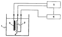
図1は本発明の実施の一例を示す針状多電極型陽極の図である。 FIG. 1 is a diagram of a needle-shaped multi-electrode anode showing an example of implementation of the present invention.
Ni−W合金を作製する電解析出法においては、電解浴槽内にて局所電位制御により、意図的に合金中のW含有量を局所的に制御できることが確認された。本発明の電解析出法では図1に示すように複数の電解析出用電極群として針状の多電極型陽極1を2次元的に剣山状に配列し、それぞれにポテンシオ・ガルバノスタット精密電源3を接続して、別々に電位制御する。 In the electrolytic deposition method for producing the Ni—W alloy, it was confirmed that the W content in the alloy can be intentionally controlled locally by controlling the local potential in the electrolytic bath. In the electrolytic deposition method of the present invention, as shown in FIG. 1, a plurality of electrode-
図2は本発明の多電極型陽極を用いた電解析出法の概念図を示す。当該精密電源3の各々にはパルス時間波形電流供給機能が付与されており、これらの動作を設定プログラムを持つ制御装置4で制御することにより、各電極の電流を時間的に独立に制御する。これにより、電析時の面方向・厚さ方向に電位分布を与え、その時間制御を行い、3次元的な電析制御を行う。 FIG. 2 shows a conceptual diagram of the electrolytic deposition method using the multielectrode anode of the present invention. Each of the
電析面の角の4箇所には白金標準電位計測用電極2を配置して電解液中の平均電位を常にモニターし、その信号を制御装置4にフィードバックすることにより電析速度の安定化、均一化を確保する。 The platinum standard
高強度Ni−Wナノ結晶電解析出合金の製法(特開2001−342591号,山崎他)によれば、電解析出時に付加する電位、即ち電流密度を制御して、電解析出合金中のW含有量を制御することができる。 特に、W原子の電解析出にはある一定以上の臨界電位が必要とされ、その値以下では、Wは電解析出できずにNiのみの電解析出となるため、この臨界電位を中心に電位を制御することによって高強度Ni−W合金相と軟質Ni相とを選択的に析出制御することが可能である。 According to the method for producing a high-strength Ni—W nanocrystalline electrodeposited alloy (Japanese Patent Laid-Open No. 2001-342591, Yamazaki et al.), The potential applied during the electrodeposition, that is, the current density is controlled, The W content can be controlled. In particular, a critical potential of a certain level or more is required for the electrolytic deposition of W atoms. Below that value, W cannot be electrolytically deposited, but only Ni is electrolytically deposited. By controlling the potential, it is possible to selectively control the precipitation of the high-strength Ni—W alloy phase and the soft Ni phase.
本発明の電解析出法では前記多電極型陽極を用いて、電析試料の面方向・膜厚方向において要求する合金組成分布を生じさせるよう、前述の臨界電位を中心に電位を制御装置4によって制御する。特に硬質Ni−Wナノ結晶相と軟質Ni相が3次元的に交互に電解析出するよう制御する。その際、前記電位計測用電極2からのモニター信号により、フィードバック制御を同時に行う。 In the electrolytic deposition method of the present invention, the multi-electrode anode is used to control the potential around the above-mentioned critical potential so as to produce the required alloy composition distribution in the surface direction and film thickness direction of the electrodeposited sample. Control by. In particular, control is performed so that the hard Ni—W nanocrystal phase and the soft Ni phase are electrolytically deposited alternately three-dimensionally. At that time, feedback control is simultaneously performed by the monitor signal from the potential measuring
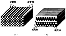
図3は上述のように人為的に制御されて生成されたナノメートルからミリメートル寸法の周期長を持つ3次元階層構造を有するNi−W電解析出複合合金の断面構造の模式図を示す。(1)は一方向型,(2)は二方向型でNi−W相とNi相とが周期的に共存した電解析出合金の断面構造を模式的に示す。 FIG. 3 is a schematic view of a cross-sectional structure of a Ni—W electrodeposited composite alloy having a three-dimensional hierarchical structure having a periodic length of nanometer to millimeter dimensions, which is artificially controlled as described above. (1) is a one-way type, and (2) is a two-way type, schematically showing a cross-sectional structure of an electrodeposited alloy in which a Ni—W phase and a Ni phase coexist periodically.
図3(1)ではナノメートルミリメートルの幅と厚さとを有する棒状の硬質相と軟質相との金属相それぞれの側面が相互に隣接して3次元階層構造を形成している。 In FIG. 3A, the side surfaces of the metal phases of the rod-like hard phase and soft phase having a width and thickness of nanometer millimeter are adjacent to each other to form a three-dimensional hierarchical structure.
図3(2)ではナノメートルからミリメートルの幅を有する棒状の硬質相と軟質相との金属相それぞれの側面が相互に隣接してナノメートルからミリメートルの等しい厚さで合金の板を形成し、当該合金の板を構成する金属相の棒の向きを隣接する板の金属相の棒の向きに対し傾斜角度を持たせつつ相互に重なり合って3次元周期性階層構造を形成している。 In FIG. 3 (2), the sides of the metal phases of the rod-like hard phase and soft phase having a width of nanometer to millimeter are adjacent to each other to form an alloy plate with an equal thickness of nanometer to millimeter, The three-dimensional periodic hierarchical structure is formed by overlapping the metal phase rods constituting the alloy plate with an inclination angle with respect to the metal phase rod directions of the adjacent plates.
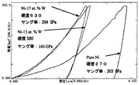
また前記電位制御により生成されたナノNi−W相とNi相の硬度・ヤング率を超微小ダイナミック硬度計により測定した例を図4に示す。 Moreover, the example which measured the hardness and the Young's modulus of the nano Ni-W phase and Ni phase which were produced | generated by the said electric potential control with an ultra micro dynamic hardness meter is shown in FIG.
純Ni相領域は、Ni−W相に比べて、同一負荷条件下におけるダイヤモンド圧子の押し込み深さが深く、軟質であることを示すが、Wを添加されたNi−W合金相領域においては、結晶粒の微細化効果とW原子の固溶効果により、大きな硬度の上昇が見られる。また、Ni−13at.%W合金領域において観察されるように、一般に結晶粒微細化効果によってヤング率の低下が生ずるが、Wの含有量を17at.%にまで増加させることにより、ヤング率を純Ni相の値とほぼ同じ値にあわせることができる。 The pure Ni phase region shows that the indentation depth of the diamond indenter under the same load condition is deeper and softer than the Ni-W phase, but in the Ni-W alloy phase region to which W is added, A large increase in hardness is observed due to the effect of refining crystal grains and the solid solution effect of W atoms. Ni-13 at. As observed in the% W alloy region, the Young's modulus is generally lowered due to the grain refinement effect, but the W content is reduced to 17 at. By increasing the ratio to%, the Young's modulus can be adjusted to substantially the same value as that of the pure Ni phase.
以上のように、本発明による合金の製造方法においては、製造条件を調節することにより、様々な硬度とヤング率の複合組織を組み合わせることが可能であり、硬質相と軟質相を複合化することにより、高強度・高延性を兼ね備えることができるとともに、ヤング率の制御された精密なバネ変形特性を有する複合合金を目的に応じて製造できる利点を有する。 As described above, in the method for producing an alloy according to the present invention, it is possible to combine composite structures of various hardnesses and Young's moduli by adjusting the production conditions, and to combine a hard phase and a soft phase. Thus, it is possible to combine high strength and high ductility, and to produce a composite alloy having precise spring deformation characteristics with a controlled Young's modulus depending on the purpose.
本発明による3次元階層構造を有する合金では上述するように優れた機械性能を示すのみならず、Ni−W合金相だけの場合と異なりNi相が共存することによって電気伝導度が大幅に増大するなど電気特性も改善されるなどの利点がある。 The alloy having a three-dimensional hierarchical structure according to the present invention not only exhibits excellent mechanical performance as described above, but also significantly increases electrical conductivity due to the coexistence of the Ni phase unlike the case of the Ni-W alloy phase alone. There are advantages such as improved electrical characteristics.
図5は本発明の電解析出法に光リソグラフィーを組み合わせて作製した3次元周期性階層構造合金の例を示す。 ナノメートルからミリメートルの断面寸法を有する棒状の軟質相のCu,Ni,Au,等が、硬質相の高強度ナノ結晶Ni−W合金の中に、ナノメートルからミリメートルの間隔で配置されている。後に図7で説明するような光リソグラフィー技術を利用してレジスト材の柱を面方向にナノメートルからミリメートルの間隔で周期的に分布させて作製した後に、厚さ方向に高強度ナノ結晶Ni−W合金などを電解析出し、次にレジスト材を除去した空洞に軟質Cu,Ni,Au,等を電解析出することによっても図5に示すような機械的、電気的性能のすぐれた3次元周期性階層構造合金を作製することができる。 FIG. 5 shows an example of a three-dimensional periodic hierarchical structure alloy produced by combining the electrolytic deposition method of the present invention with photolithography. Rod-like soft phase Cu, Ni, Au, etc. having a cross-sectional dimension of nanometers to millimeters are arranged at intervals of nanometers to millimeters in a high-strength nanocrystalline Ni—W alloy of a hard phase. After the resist material pillars are periodically distributed at intervals of nanometers to millimeters in the plane direction by using an optical lithography technique as will be described later with reference to FIG. 7, high-strength nanocrystalline Ni- 3D with excellent mechanical and electrical performance as shown in FIG. 5 by electrolytically depositing W alloy etc. and then electrolytically depositing soft Cu, Ni, Au, etc. into the cavity from which the resist material has been removed. A periodic hierarchical structure alloy can be produced.
硬質のNi−W相と軟質のNi相を前記電位制御により選択的に析出させ、3次元周期性階層構造をもつ複合材料を作製する際、ミクロに合金組成を傾斜させ、硬質Ni−Wナノ結晶相と軟質Ni相を所定の体積分率になるように調整・制御することができる。したがって、ミクロに見れば、合金組成が傾斜状態となって3次元的に配列させることができるため、機械的特性の改善には理想的な材料組織が生成される。 When producing a composite material having a three-dimensional periodic hierarchical structure by selectively precipitating a hard Ni-W phase and a soft Ni phase by the above-described potential control, the alloy composition is tilted microscopically, The crystal phase and the soft Ni phase can be adjusted and controlled to have a predetermined volume fraction. Therefore, when viewed microscopically, the alloy composition can be three-dimensionally arranged in an inclined state, so that an ideal material structure is generated for improving the mechanical characteristics.
従来の材料組織学的手法を用いた場合、硬質と軟質の両相界面は明確な境界面を形成し、界面剥離等による材料の劣化が問題となることが多い。本発明により作製された合金は、これらの材料学的問題を解決でき、高強度・高延性を兼ね備え、耐磨耗性等の優れた新材料の作製が可能である。 When a conventional material histological method is used, the hard and soft phase interfaces form a clear boundary surface, and deterioration of the material due to interfacial peeling or the like often becomes a problem. The alloy produced according to the present invention can solve these material problems, and can produce a new material having both high strength and high ductility and excellent wear resistance.
図6は本発明の方法を用い、組成がミクロな傾斜状態にて3次元周期配列した合金の構造模式図を示す。硬質Ni−Wナノ結晶相と軟質Ni相を所定の体積分率になるように調整・制御することによって、これら硬質と軟質相の網目状構造を創製し、W含有量をミクロにもマクロにも傾斜させることができる。各曲線は組成値の等高線を表す。例えばNi−W合金は電析時に残留応力を発生し易いが、このような3次元合金組成制御法を利用して残留応力を抑制することが可能である。 FIG. 6 shows a structural schematic diagram of an alloy in which the method of the present invention is used and the composition is three-dimensionally periodically arranged in a tilted state. By adjusting and controlling the hard Ni-W nanocrystal phase and the soft Ni phase so as to have a predetermined volume fraction, a network structure of these hard and soft phases is created, and the W content is made micro and macro. Can also be tilted. Each curve represents a contour line of the composition value. For example, Ni-W alloy tends to generate residual stress during electrodeposition, but it is possible to suppress the residual stress by using such a three-dimensional alloy composition control method.
図7は本発明に係る3次元周期性階層構造をもつ複合材料を用いたマイクロ構造体の製造方法の一例を示す。 FIG. 7 shows an example of a method for manufacturing a microstructure using a composite material having a three-dimensional periodic hierarchical structure according to the present invention.
図7(1)はフォトマスク7を通して、導電性基板8上に塗布した感光性樹脂;レジスト材9に放射光もしくは紫外線10を照射して露光するステップを示す。 FIG. 7 (1) shows a step of exposing the photosensitive material; resist
図7(2)は感光性樹脂の現像のステップを示す。フォトマスク7の中で「IMT」と表示されたパターン11は放射光または紫外線10を吸収する光吸収体からなり、フォトマスク7の光吸収体パターン11を除く部分を透過した光により、その光に露光された部分の感光性樹脂;レジスト材9の分子鎖が切れ、特定の現像液に選択的に溶解するようになる。この現像処理により、導電性基板8上に感光性樹脂;レジスト材9からなるマイクロ構造体12が形成される。 FIG. 7 (2) shows a development step of the photosensitive resin. The
図7(3)は電解析出法による金属堆積のステップを示す。感光性樹脂9が溶解した部分に、本発明に係る3次元周期性階層構造をもつ高強度・高延性複合合金を上記電解析出法にしたがって電解析出させる。 FIG. 7 (3) shows a step of metal deposition by electrolytic deposition. A high strength / high ductility composite alloy having a three-dimensional periodic hierarchical structure according to the present invention is electrolytically deposited in a portion where the
図7(4)は残存樹脂の除去のステップを示す。残った感光性樹脂を溶剤で取り除くことにより、3次元周期性階層構造をもつ高強度・高延性複合合金のマイクロ構造体13が得られる。この方法によれば、機械加工法では成形が困難なマイクロメータサイズの微小な構造体の成形が可能であり、フォトマスクの光吸収体の形状を変えることにより、任意の構造のマイクロ構造体の成形が可能である。 FIG. 7 (4) shows a step of removing the residual resin. By removing the remaining photosensitive resin with a solvent, a
一般に、に示すように、レジスト材などに光リソグラフィー法を用いて微小パターンを焼付け現像することによって作製した立体空洞中にて電析による合金生成を行うことによって合金の成型をも同時に行うことが出来る。 In general, as shown in FIG. 5, it is possible to simultaneously form an alloy by forming an alloy by electrodeposition in a three-dimensional cavity produced by baking and developing a micropattern on a resist material using a photolithographic method. I can do it.
本発明によって生成される3次元周期性階層構造をもつ複合材料の生成を上述のような成形の型の中で行うことによって、高機能な機械特性を具備した微小合金構造体を大量に製造することが出来る。 By producing the composite material having the three-dimensional periodic hierarchical structure generated by the present invention in the mold as described above, a large amount of microalloy structures having high-functional mechanical properties are manufactured. I can do it.
以上説明したように本発明により、3次元の最適な周期性階層構造をもち、その周期長がナノメートルからミリメートルの寸法であることを特徴とする複合材構造を人為的に大量に創製することができる。 As described above, the present invention artificially creates a large number of composite structures characterized by having a three-dimensional optimal periodic hierarchical structure and having a period length of nanometers to millimeters. Can do.
したがって、硬質・高塑性変形能を有し、電気特性の優れた新しい高機能材料・部品を安価に提供することができる。 Therefore, it is possible to provide a new high-functional material / part having a hard and high plastic deformability and excellent electrical characteristics at low cost.
1 電解浴槽
2 多電極型陽極。
3 陰極
4 白金標準電位計測用電極。
5 ポテンシオ・ガルバノスタット精密電源。
6 制御装置
7 フォトマスク
8 導電性基板
9 レジスト材
10 放射光、紫外線
11 パターン
12 露光・現像後に残存したレジスト材
13 電析合金によるマイクロ構造体1
3
5 Potentio galvanostat precision power supply.
6
Claims (10)
Priority Applications (2)
| Application Number | Priority Date | Filing Date | Title |
|---|---|---|---|
| JP2003343794A JP2005068546A (en) | 2003-08-26 | 2003-08-26 | Multiple alloy with three-dimensional periodic hierarchical structure, and its production method |
| US10/924,970 US7473328B2 (en) | 2003-08-26 | 2004-08-25 | Composite alloy having a three-dimensional periodic hierarchical structure and method of producing the same |
Applications Claiming Priority (1)
| Application Number | Priority Date | Filing Date | Title |
|---|---|---|---|
| JP2003343794A JP2005068546A (en) | 2003-08-26 | 2003-08-26 | Multiple alloy with three-dimensional periodic hierarchical structure, and its production method |
Publications (2)
| Publication Number | Publication Date |
|---|---|
| JP2005068546A true JP2005068546A (en) | 2005-03-17 |
| JP2005068546A5 JP2005068546A5 (en) | 2005-05-26 |
Family
ID=34214282
Family Applications (1)
| Application Number | Title | Priority Date | Filing Date |
|---|---|---|---|
| JP2003343794A Pending JP2005068546A (en) | 2003-08-26 | 2003-08-26 | Multiple alloy with three-dimensional periodic hierarchical structure, and its production method |
Country Status (2)
| Country | Link |
|---|---|
| US (1) | US7473328B2 (en) |
| JP (1) | JP2005068546A (en) |
Cited By (2)
| Publication number | Priority date | Publication date | Assignee | Title |
|---|---|---|---|---|
| CN1696353B (en) * | 2005-05-16 | 2010-05-12 | 山东科技大学 | Method for making Nano surface of metal material |
| JP7391356B2 (en) | 2019-09-04 | 2023-12-05 | 兵庫県公立大学法人 | Multilayer material and its manufacturing method, multilayer material plating method |
Families Citing this family (12)
| Publication number | Priority date | Publication date | Assignee | Title |
|---|---|---|---|---|
| JP2005146405A (en) * | 2003-11-14 | 2005-06-09 | Toru Yamazaki | Electrodeposition stacked alloy thin sheet, and its production method |
| BE1018130A3 (en) * | 2008-09-19 | 2010-05-04 | Magotteaux Int | HIERARCHICAL COMPOSITE MATERIAL. |
| EP2754735B1 (en) * | 2013-01-11 | 2020-07-22 | Elsyca N.V. | A device suitable for the electrochemical processing of an object, and a method for the electrochemical processing of an object |
| US9677191B2 (en) | 2013-01-17 | 2017-06-13 | Elsyca N.V. | Device suitable for the electrochemical processing of an object, a holder suitable for such a device, and a method for the electrochemical processing of an object |
| WO2017087884A1 (en) * | 2015-11-19 | 2017-05-26 | Fabric8Labs, Inc. | Three dimensional additive manufacturing of metal objects by stereo-electrochemical deposition |
| CN110172655B (en) * | 2019-04-19 | 2021-05-04 | 武汉理工大学 | Gradient metal material with nanocrystalline or ultrafine grain inside coarse grain of surface layer and preparation method thereof |
| US10914000B1 (en) | 2019-08-23 | 2021-02-09 | Fabric8Labs, Inc. | Method for manufacturing a printhead of an electrochemical additive manufacturing system |
| US11512404B2 (en) | 2019-08-23 | 2022-11-29 | Fabric8Labs, Inc. | Matrix-controlled printhead for an electrochemical additive manufacturing system |
| US11680330B2 (en) | 2021-07-22 | 2023-06-20 | Fabric8Labs, Inc. | Electrochemical-deposition apparatuses and associated methods of electroplating a target electrode |
| US11795561B2 (en) | 2021-08-02 | 2023-10-24 | Fabric8Labs, Inc. | Electrochemical-deposition system, apparatus, and method using optically-controlled deposition electrodes |
| US11920251B2 (en) | 2021-09-04 | 2024-03-05 | Fabric8Labs, Inc. | Systems and methods for electrochemical additive manufacturing of parts using multi-purpose build plate |
| US11745432B2 (en) | 2021-12-13 | 2023-09-05 | Fabric8Labs, Inc. | Using target maps for current density control in electrochemical-additive manufacturing systems |
Family Cites Families (7)
| Publication number | Priority date | Publication date | Assignee | Title |
|---|---|---|---|---|
| US5641391A (en) * | 1995-05-15 | 1997-06-24 | Hunter; Ian W. | Three dimensional microfabrication by localized electrodeposition and etching |
| US6261469B1 (en) * | 1998-10-13 | 2001-07-17 | Honeywell International Inc. | Three dimensionally periodic structural assemblies on nanometer and longer scales |
| US6409907B1 (en) * | 1999-02-11 | 2002-06-25 | Lucent Technologies Inc. | Electrochemical process for fabricating article exhibiting substantial three-dimensional order and resultant article |
| JP2001342591A (en) | 2000-03-27 | 2001-12-14 | Takayasu Mochizuki | High strength alloy and manufacturing method, and coated metal with high strength alloy and micro structural body using it |
| US20020197042A1 (en) * | 2001-04-06 | 2002-12-26 | Shigeo Kittaka | Optical device, and wavelength multiplexing optical recording head |
| GB2390230B (en) * | 2002-06-07 | 2005-05-25 | Murata Manufacturing Co | Applications of a three dimensional structure |
| JP4612844B2 (en) * | 2004-02-23 | 2011-01-12 | キヤノン株式会社 | Three-dimensional periodic structure and functional element having the same |
-
2003
- 2003-08-26 JP JP2003343794A patent/JP2005068546A/en active Pending
-
2004
- 2004-08-25 US US10/924,970 patent/US7473328B2/en not_active Expired - Fee Related
Cited By (2)
| Publication number | Priority date | Publication date | Assignee | Title |
|---|---|---|---|---|
| CN1696353B (en) * | 2005-05-16 | 2010-05-12 | 山东科技大学 | Method for making Nano surface of metal material |
| JP7391356B2 (en) | 2019-09-04 | 2023-12-05 | 兵庫県公立大学法人 | Multilayer material and its manufacturing method, multilayer material plating method |
Also Published As
| Publication number | Publication date |
|---|---|
| US20050045252A1 (en) | 2005-03-03 |
| US7473328B2 (en) | 2009-01-06 |
Similar Documents
| Publication | Publication Date | Title |
|---|---|---|
| JP2005068546A (en) | Multiple alloy with three-dimensional periodic hierarchical structure, and its production method | |
| DE60225352T2 (en) | METHOD OF ELECTROPLATING METALLIC AND METAL MATRIX COMPOSITE FILMS, COATINGS AND MICROCOMPONENTS | |
| Hasegawa et al. | Orientation-controlled nanotwinned copper prepared by electrodeposition | |
| US8906216B2 (en) | Method for producing alloy deposits and controlling the nanostructure thereof using electro-deposition with controlled polarity ratio | |
| Burek et al. | Fabrication and microstructure control of nanoscale mechanical testing specimens via electron beam lithography and electroplating | |
| Pavithra et al. | Controllable crystallographic texture in copper foils exhibiting enhanced mechanical and electrical properties by pulse reverse electrodeposition | |
| Chen et al. | Pulse electroplating of ultra-fine grained Au films with high compressive strength | |
| JP2005068546A5 (en) | ||
| Ren et al. | Localized electrodeposition micro additive manufacturing of pure copper microstructures | |
| DE10228323B4 (en) | Cathodic electrodeposition process and microcomponents made by such a process | |
| Dai et al. | Study on Cu-Al2O3 metal-matrix composite coating prepared by Laser-assisted electrodeposition | |
| DE202016007550U1 (en) | Electroplated copper alloys with high strength and conductivity | |
| US11063120B2 (en) | Metal-graphene structures forming a lattice of interconnected segments | |
| Xiao et al. | Ultrahigh strength ultrapure nanostructured nickel metal prepared via ultrafine anode scanning electrodeposition | |
| Song et al. | Reducing the residual stress in micro electroforming layer by megasonic agitation | |
| Bacal et al. | Electrodeposition of high-tungsten W-Ni-Cu alloys. Impact of copper on deposition process and coating structure | |
| JP2001342591A (en) | High strength alloy and manufacturing method, and coated metal with high strength alloy and micro structural body using it | |
| US6824668B2 (en) | Method for electroplating Ni-Fe-P alloys using sulfamate solution | |
| CN100345996C (en) | Nanometer crystal-micro crystal layered composite material and its preparation method | |
| RU2322532C2 (en) | Method for electrodeposition of copper | |
| CN107385486A (en) | The method of pulse plating gold and the gold plate of formation | |
| Karim et al. | Tuning the characteristics of electrochemically fabricated gold nanowires | |
| Apolinário et al. | Bottom-up nanofabrication using self-organized porous templates | |
| JP4243281B2 (en) | High-strength alloy, metal material coated with the high-strength alloy, and microstructure using the high-strength alloy | |
| Schürch | Template-assisted electrodeposition of nickel and nickel copper 3D microcomponents |
Legal Events
| Date | Code | Title | Description |
|---|---|---|---|
| A521 | Request for written amendment filed |
Free format text: JAPANESE INTERMEDIATE CODE: A523 Effective date: 20041201 |
|
| A521 | Request for written amendment filed |
Free format text: JAPANESE INTERMEDIATE CODE: A523 Effective date: 20040826 |
|
| A521 | Request for written amendment filed |
Free format text: JAPANESE INTERMEDIATE CODE: A523 Effective date: 20040826 |