JP2005039067A - Nonvolatile semiconductor storage device - Google Patents
Nonvolatile semiconductor storage device Download PDFInfo
- Publication number
- JP2005039067A JP2005039067A JP2003274728A JP2003274728A JP2005039067A JP 2005039067 A JP2005039067 A JP 2005039067A JP 2003274728 A JP2003274728 A JP 2003274728A JP 2003274728 A JP2003274728 A JP 2003274728A JP 2005039067 A JP2005039067 A JP 2005039067A
- Authority
- JP
- Japan
- Prior art keywords
- impurity diffusion
- floating gate
- region
- semiconductor substrate
- type
- Prior art date
- Legal status (The legal status is an assumption and is not a legal conclusion. Google has not performed a legal analysis and makes no representation as to the accuracy of the status listed.)
- Withdrawn
Links
- 239000004065 semiconductor Substances 0.000 title claims abstract description 114
- 238000009792 diffusion process Methods 0.000 claims abstract description 138
- 239000012535 impurity Substances 0.000 claims abstract description 136
- 239000000758 substrate Substances 0.000 claims abstract description 79
- 238000002955 isolation Methods 0.000 claims description 17
- 230000015572 biosynthetic process Effects 0.000 claims description 5
- 238000009413 insulation Methods 0.000 abstract 1
- 239000010410 layer Substances 0.000 description 34
- 239000000969 carrier Substances 0.000 description 12
- 230000005641 tunneling Effects 0.000 description 12
- 239000002356 single layer Substances 0.000 description 7
- 230000000694 effects Effects 0.000 description 6
- 239000002784 hot electron Substances 0.000 description 4
- 238000004519 manufacturing process Methods 0.000 description 2
- 230000008878 coupling Effects 0.000 description 1
- 238000010168 coupling process Methods 0.000 description 1
- 238000005859 coupling reaction Methods 0.000 description 1
- 229910044991 metal oxide Inorganic materials 0.000 description 1
- 150000004706 metal oxides Chemical class 0.000 description 1
- 238000012986 modification Methods 0.000 description 1
- 230000004048 modification Effects 0.000 description 1
- 238000013519 translation Methods 0.000 description 1
- 230000014616 translation Effects 0.000 description 1
Images


Classifications
-
- H—ELECTRICITY
- H10—SEMICONDUCTOR DEVICES; ELECTRIC SOLID-STATE DEVICES NOT OTHERWISE PROVIDED FOR
- H10B—ELECTRONIC MEMORY DEVICES
- H10B41/00—Electrically erasable-and-programmable ROM [EEPROM] devices comprising floating gates
- H10B41/30—Electrically erasable-and-programmable ROM [EEPROM] devices comprising floating gates characterised by the memory core region
-
- E—FIXED CONSTRUCTIONS
- E04—BUILDING
- E04G—SCAFFOLDING; FORMS; SHUTTERING; BUILDING IMPLEMENTS OR AIDS, OR THEIR USE; HANDLING BUILDING MATERIALS ON THE SITE; REPAIRING, BREAKING-UP OR OTHER WORK ON EXISTING BUILDINGS
- E04G17/00—Connecting or other auxiliary members for forms, falsework structures, or shutterings
- E04G17/14—Bracing or strutting arrangements for formwalls; Devices for aligning forms
-
- H—ELECTRICITY
- H01—ELECTRIC ELEMENTS
- H01L—SEMICONDUCTOR DEVICES NOT COVERED BY CLASS H10
- H01L29/00—Semiconductor devices adapted for rectifying, amplifying, oscillating or switching, or capacitors or resistors with at least one potential-jump barrier or surface barrier, e.g. PN junction depletion layer or carrier concentration layer; Details of semiconductor bodies or of electrodes thereof ; Multistep manufacturing processes therefor
- H01L29/66—Types of semiconductor device ; Multistep manufacturing processes therefor
- H01L29/68—Types of semiconductor device ; Multistep manufacturing processes therefor controllable by only the electric current supplied, or only the electric potential applied, to an electrode which does not carry the current to be rectified, amplified or switched
- H01L29/76—Unipolar devices, e.g. field effect transistors
- H01L29/772—Field effect transistors
- H01L29/78—Field effect transistors with field effect produced by an insulated gate
- H01L29/788—Field effect transistors with field effect produced by an insulated gate with floating gate
- H01L29/7881—Programmable transistors with only two possible levels of programmation
- H01L29/7883—Programmable transistors with only two possible levels of programmation charging by tunnelling of carriers, e.g. Fowler-Nordheim tunnelling
-
- H—ELECTRICITY
- H10—SEMICONDUCTOR DEVICES; ELECTRIC SOLID-STATE DEVICES NOT OTHERWISE PROVIDED FOR
- H10B—ELECTRONIC MEMORY DEVICES
- H10B41/00—Electrically erasable-and-programmable ROM [EEPROM] devices comprising floating gates
- H10B41/60—Electrically erasable-and-programmable ROM [EEPROM] devices comprising floating gates the control gate being a doped region, e.g. single-poly memory cell
-
- H—ELECTRICITY
- H10—SEMICONDUCTOR DEVICES; ELECTRIC SOLID-STATE DEVICES NOT OTHERWISE PROVIDED FOR
- H10B—ELECTRONIC MEMORY DEVICES
- H10B69/00—Erasable-and-programmable ROM [EPROM] devices not provided for in groups H10B41/00 - H10B63/00, e.g. ultraviolet erasable-and-programmable ROM [UVEPROM] devices
Abstract
Description
本発明は、不揮発性半導体記憶装置に関し、特に、単層ゲート構造のメモリセルを有する不揮発性半導体記憶装置に関するものである。 The present invention relates to a nonvolatile semiconductor memory device, and more particularly to a nonvolatile semiconductor memory device having a memory cell having a single layer gate structure.
従来のフラッシュメモリのメモリセルは、チャネル領域上にトンネル酸化膜を介してフローティングゲートが形成され、さらに絶縁膜を介してフローティングゲート上にコントロールゲートが形成された積層ゲート構造を有している。しかし、このような積層ゲート構造では構成および製造工程が複雑となる。 A memory cell of a conventional flash memory has a stacked gate structure in which a floating gate is formed on a channel region via a tunnel oxide film, and a control gate is formed on the floating gate via an insulating film. However, such a stacked gate structure complicates the configuration and the manufacturing process.
これに対して、構成および製造工程を簡易にするために、チャネル領域上のゲートをフローティングゲートのみとした単層ゲート構造のメモリセルが提案されている。 On the other hand, in order to simplify the configuration and the manufacturing process, a memory cell having a single-layer gate structure in which the gate on the channel region has only a floating gate has been proposed.
従来の単層ゲート構造のメモリセルでは、基板とフローティングゲートとが容量結合をしているため、基板に電圧を与えるとフローティングゲートの電位も自動的に基板の電位と近い値となってしまう。このため、基板とフローティングゲートとの間に大きな電位差を与えることが困難であった。 In a conventional memory cell having a single-layer gate structure, since the substrate and the floating gate are capacitively coupled, when a voltage is applied to the substrate, the potential of the floating gate automatically becomes a value close to the potential of the substrate. For this reason, it is difficult to give a large potential difference between the substrate and the floating gate.
このため、電気的に消去を行うことがほぼ不可能であり、紫外線照射による消去のみが可能であるため、従来の単層ゲート構造のメモリセルはOTPROM(One Time Programmable Read-Only Memory)などのほとんど書き換えを行なわない用途にしか使用できなかった。 For this reason, it is almost impossible to perform erasing electrically, and only erasing by ultraviolet irradiation is possible. Therefore, a conventional memory cell having a single-layer gate structure is an OTPROM (One Time Programmable Read-Only Memory) or the like. It could only be used for applications that were hardly rewritten.
また、単層ゲート構造のメモリセルにおいて、電気的に消去可能な構成が、たとえば特表平8−506693号公報、特開平3−57280号公報などに開示されている。 In addition, in a memory cell having a single-layer gate structure, an electrically erasable configuration is disclosed, for example, in Japanese translations of PCT publication No. 8-506669 and Japanese Patent Laid-Open No. 3-57280.
この構成によれば、半導体基板の表面に形成された不純物拡散領域をフローティングゲートに対向させることにより、この不純物拡散領域によるフローティングゲートの電位の制御が可能とされている。
しかしながら、上記2つの公報に開示されたメモリトランジスタはnチャネルMOS(Metal Oxide Semiconductor)トランジスタであり、低電圧でのデータの書き込みが困難であるという問題点があった。以下、そのことについて説明する。 However, the memory transistors disclosed in the above two publications are n-channel MOS (Metal Oxide Semiconductor) transistors, and there is a problem that it is difficult to write data at a low voltage. This will be described below.
メモリトランジスタがnチャネルMOSトランジスタの場合、書き込み動作においてはドレインに高い正の電圧を印加することにより、ソースから引き出された電子が半導体基板表面のチャネル内をドレインに向って高速で走り、ドレイン近傍でホットエレクトロンと呼ばれる高エネルギー状態となる。このホットエレクトロンが、フローティングゲートに注入されて、データの書き込まれた状態となる。 When the memory transistor is an n-channel MOS transistor, by applying a high positive voltage to the drain in the write operation, electrons drawn from the source run at high speed in the channel on the surface of the semiconductor substrate toward the drain, and in the vicinity of the drain It becomes a high energy state called hot electron. This hot electron is injected into the floating gate, and data is written.
この場合、ドレインに高い正の電圧が印加されているため、ホットエレクトロンは、半導体基板とフローティングゲートとの間に大きな電位差を与えないと、ドレイン側へ注入されるだけでフローティングゲートに注入され難くなる。このため、メモリトランジスタがnチャネルMOSトランジスタの場合には、書き込み動作時において高電圧を印加しなければならず、低電圧でのデータの書き込みが困難であるという問題点があった。 In this case, since a high positive voltage is applied to the drain, hot electrons are not injected into the floating gate only by being injected into the drain side unless a large potential difference is given between the semiconductor substrate and the floating gate. Become. For this reason, when the memory transistor is an n-channel MOS transistor, a high voltage must be applied during the write operation, and there is a problem that it is difficult to write data at a low voltage.
特に、単層ゲート構造の場合には、フローティングゲート上にコントロールゲートがないため、フローティングゲートと半導体基板との間の容量結合による電位差でホットエレクトロンをフローティングゲートに注入しなければならない。このように高電圧を与えないとデータの書き込みが困難であるが、単層ゲート構造においては高電位を与えることも難しいため、データの書き込み動作が困難になるという問題があった。 In particular, in the case of a single-layer gate structure, since there is no control gate on the floating gate, hot electrons must be injected into the floating gate by a potential difference due to capacitive coupling between the floating gate and the semiconductor substrate. As described above, it is difficult to write data unless a high voltage is applied. However, in a single-layer gate structure, it is difficult to apply a high potential, and thus there is a problem that a data writing operation is difficult.
それゆえ本発明の目的は、電気的にデータを消去可能で、かつ低電圧でのデータの書き込みが容易な不揮発性半導体装置を提供することを目的とする。 Therefore, an object of the present invention is to provide a nonvolatile semiconductor device in which data can be electrically erased and data can be easily written at a low voltage.
本発明の不揮発性半導体記憶装置は、半導体基板と、ソース/ドレインとなる1対のp型不純物拡散領域と、フローティングゲートと、制御用不純物拡散領域とを備えている。半導体基板は、主表面を有している。ソース/ドレインとなる1対のp型不純物拡散領域は、半導体基板の主表面に形成されている。フローティングゲートは、1対のp型不純物拡散領域に挟まれる半導体基板の領域の上にトンネル絶縁層を介して形成されている。制御用不純物拡散領域は、半導体基板の主表面に形成されており、フローティングゲートの電位を制御するためのものである。 The nonvolatile semiconductor memory device of the present invention includes a semiconductor substrate, a pair of p-type impurity diffusion regions serving as source / drain, a floating gate, and a control impurity diffusion region. The semiconductor substrate has a main surface. A pair of p-type impurity diffusion regions serving as source / drain is formed on the main surface of the semiconductor substrate. The floating gate is formed on a region of the semiconductor substrate sandwiched between the pair of p-type impurity diffusion regions via a tunnel insulating layer. The control impurity diffusion region is formed on the main surface of the semiconductor substrate and is for controlling the potential of the floating gate.
本発明の不揮発性半導体装置によれば、フローティングゲートの電位を制御するための制御用不純物拡散領域が半導体基板の主表面に形成されているため、基板とフローティングゲートとの間に大きな電位差を与えることが容易となる。これにより、フローティングゲートの電子を引き抜くことが容易となり、電気的な消去が可能となる。 According to the nonvolatile semiconductor device of the present invention, since the control impurity diffusion region for controlling the potential of the floating gate is formed on the main surface of the semiconductor substrate, a large potential difference is given between the substrate and the floating gate. It becomes easy. Thereby, it becomes easy to extract the electrons of the floating gate, and electrical erasure becomes possible.
また、ソース/ドレインがp型の不純物拡散領域であるため、メモリトランジスタはpチャネルのトランジスタである。このpチャネルのトランジスタの場合、書き込み動作時においてはドレインに負側の電圧を印加することにより、ソースから供給された正孔が半導体基板表面のチャネル内をドレインに向って高速で走り、ドレイン近傍で原子と衝突して電子−正孔対を生じさせる。そして、その電子−正孔対の電子が、フローティングゲートに注入されて、データの書き込まれた状態となる。 Further, since the source / drain is a p-type impurity diffusion region, the memory transistor is a p-channel transistor. In the case of this p-channel transistor, when a negative voltage is applied to the drain during the write operation, holes supplied from the source run at high speed in the channel on the surface of the semiconductor substrate toward the drain, and in the vicinity of the drain. To collide with atoms to generate electron-hole pairs. Then, the electrons of the electron-hole pair are injected into the floating gate, and the data is written.
この場合、ドレインに印加される電圧は負側の電圧であるため、電子はドレイン側に注入され難く、ゲート側に注入され易くなる。このため、半導体基板とフローティングゲートとの間にそれほど大きな電位差を与えなくとも、電子をフローティングゲートに注入することができ、低電圧でのデータの書き込みが可能となる。 In this case, since the voltage applied to the drain is a negative voltage, electrons are not easily injected into the drain side and are easily injected into the gate side. Therefore, electrons can be injected into the floating gate without writing a large potential difference between the semiconductor substrate and the floating gate, and data can be written at a low voltage.
以下、本発明の実施の形態について図に基づいて説明する。 Hereinafter, embodiments of the present invention will be described with reference to the drawings.
(実施の形態1)
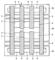
図1は、本発明の実施の形態1における半導体記憶装置の構成を概略的に示す平面図である。図2(a)および図2(b)は、図1のIIA−IIA線に沿う概略断面図および図1のIIB−IIB線に沿う概略断面図である。図3は、図1のIII−III線に沿う概略断面図である。
(Embodiment 1)
FIG. 1 is a plan view schematically showing a configuration of the semiconductor memory device according to the first embodiment of the present invention. 2A and 2B are a schematic cross-sectional view taken along line IIA-IIA in FIG. 1 and a schematic cross-sectional view taken along line IIB-IIB in FIG. 3 is a schematic cross-sectional view taken along line III-III in FIG.
なお、本来、メモリセルはビット毎に選択用のトランジスタを有しているが、選択用のトランジスタは本実施の形態の動作原理と無関係であるため、図1以外では図示せず、その説明も省略する。また、選択用のトランジスタの取扱いについては他の実施の形態についても同様である。 Note that the memory cell originally has a selection transistor for each bit, but the selection transistor is irrelevant to the operation principle of the present embodiment, so it is not shown except for FIG. Omitted. The handling of the selection transistor is the same in the other embodiments.
図1〜図3を参照して、本実施の形態のメモリセルは、フローティングゲートトランジスタ10と、フローティングゲート5をコントロールする部分とを主に有している。
1 to 3, the memory cell of the present embodiment mainly has a
図2(a)を参照して、フローティングゲートトランジスタ形成領域においては、p型の半導体基板1の主表面にn型ウェル領域2aが形成されており、n型ウェル領域2aにpチャネルMOSトランジスタであるフローティングゲートトランジスタ10が形成されている。フローティングゲートトランジスタ10は、ソース/ドレインとなる1対のp型不純物拡散領域3、3と、トンネル絶縁層4aと、フローティングゲート5とを有している。ソース/ドレインとなる1対のp型不純物拡散領域3、3は、n型ウェル領域2a内の半導体基板1の主表面に形成されている。フローティングゲート5は、1対のp型不純物拡散領域3、3に挟まれる半導体基板1の領域の上にトンネル絶縁層4aを介して形成されている。
Referring to FIG. 2A, in the floating gate transistor formation region, an n-
図2(b)を参照して、フローティングゲート5は、フローティングゲートトランジスタ形成領域からフローティングゲートコントロール領域まで延在している。このフローティングゲートコントロール領域においては、フローティングゲート5の電位を制御するための制御用不純物拡散領域6が形成されている。この制御用不純物拡散領域6は、半導体基板1の主表面に形成されたp型の不純物拡散領域より構成されており、フローティングゲート5と絶縁層4bを介して対向している。この制御用不純物拡散領域6は、半導体基板1の主表面に形成されたn型ウェル領域2b内に形成されている。
Referring to FIG. 2B,
図3を参照して、フローティングゲートトランジスタ形成領域とフローティングゲートコントロール領域との間の半導体基板1の主表面には、フィールド絶縁層7が形成されている。このフィールド絶縁層7の直下は、半導体基板1のp型領域が位置している。
Referring to FIG. 3,
次に、本実施の形態におけるメモリセルの書き込みおよび消去の動作について説明する。 Next, writing and erasing operations of the memory cell in this embodiment will be described.
なお、本実施の形態におけるメモリセルの「書き込み」状態とはフローティングゲート5に電子が蓄積された状態のことを言い、「消去」状態とはフローティングゲート5から電子が引抜かれた状態のことを言う。
In this embodiment, the “written” state of the memory cell means a state where electrons are accumulated in the
図2(a)および図2(b)を参照して、メモリセルへの書き込みは、フローティングゲートトランジスタ10でのインパクトイオン化により発生するホットキャリアをフローティングゲート5に注入することにより行なわれる。ホットキャリアの発生は、表1に示した電圧を各領域に与えることにより起こる。
Referring to FIGS. 2A and 2B, writing to the memory cell is performed by injecting hot carriers generated by impact ionization in

この際、制御用不純物拡散領域6は、フローティングゲート5の電位をコントロールする役割を担っている。具体的には、ホットキャリアの発生はフローティングゲート5の(一方のp型不純物拡散領域3から見た)電位が−1V程度の時に最も多くなるため、そのような電位になるように制御用不純物拡散領域6に電圧が与えられてフローティングゲート5の電位がコントロールされる。
At this time, the control
また、メモリセルの消去は、フローティングゲート5に蓄積された電子を一方のp型不純物拡散領域3、他方のp型不純物拡散領域3およびn型ウェル領域2aのそれぞれに高電位を与えてFN(Fowler-Nordheim)トンネリングによって引き抜くことで行なわれる。FNトンネリングを起こすために、一方のp型不純物拡散領域3、他方のp型不純物拡散領域3およびn型ウェル領域2aのそれぞれに表2に示すような正の電位が与えられる。
For erasing the memory cell, electrons stored in the floating
この際、制御用不純物拡散領域6にも表2に示すような負の電圧を与えて、フローティングゲート5の(一方のp型不純物拡散領域3から見た)電位が下げられている。効率よく消去を行うためには、フローティングゲート5と一方のp型不純物拡散領域3、他方のp型不純物拡散領域3およびn型ウェル領域2aのそれぞれとの間の接合容量比をできるだけ小さくして電位差を大きくすることが望ましい。
At this time, a negative voltage as shown in Table 2 is also applied to the control
本実施の形態のよれば、制御用不純物拡散領域6によりフローティングゲート5の電位をコントロールすることができるため、半導体基板1とフローティングゲート5との間に大きな電位差を与えることが可能となる。これにより、フローティングゲート5内の電子をFNトンネリングで引き抜くことが可能となるため、データの電気的な消去が可能となる。
According to this embodiment, since the potential of the floating
また、フローティングゲートトランジスタ10がpチャネルMOSトランジスタよりなっている。このため、書き込み動作時においてはドレインに負側の電圧を印加することにより、ソースから供給された正孔が半導体基板1表面のチャネル内をドレインに向って高速で走り、ドレイン近傍で原子と衝突して電子−正孔対を生じさせる。そして、その電子−正孔対の電子が、フローティングゲート5に注入されて、データの書き込まれた状態となる。
The floating
この場合、ドレインに印加される電圧は負側の電圧であるため、電子はドレイン側に注入され難く、フローティングゲート5側に注入され易くなる。このため、半導体基板1とフローティングゲート5との間にそれほど大きな電位差を与えなくとも、電子をフローティングゲート5に注入することができ、低電圧でのデータの書き込みが可能となる。
In this case, since the voltage applied to the drain is a negative voltage, electrons are not easily injected into the drain side and are easily injected into the floating
(実施の形態2)
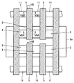
図4は、本発明の実施の形態2における半導体記憶装置の構成を概略的に示す平面図である。図5は、図4のV−V線に沿う概略断面図である。
(Embodiment 2)
FIG. 4 is a plan view schematically showing a configuration of the semiconductor memory device according to the second embodiment of the present invention. FIG. 5 is a schematic cross-sectional view taken along line VV in FIG.
図4および図5を参照して、本実施の形態のメモリセルの構成は、実施の形態1の構成と比較して、素子分離用のp型不純物拡散領域8を有している点において異なる。
4 and 5, the configuration of the memory cell of the present embodiment is different from that of the first embodiment in that p-type
この素子分離用のp型不純物拡散領域8は、フローティングゲートトランジスタ領域とフローティングゲートコントロール領域との間の半導体基板1の主表面に形成されたフィールド絶縁層7の直下の半導体基板1に形成されている。この素子分離用のp型不純物拡散領域8は、半導体基板1よりも高いキャリア濃度を有している。
The element isolation p-type
なお、上記以外の構成については実施の形態1の構成とほぼ同じであるため、同一の構成要素については同一の符号を付し、その説明を省略する。
In addition, since it is substantially the same as the structure of
本実施の形態によれば、以下の効果が得られる。 According to the present embodiment, the following effects can be obtained.
書き込みおよび消去時には表1および表2に示すような電圧がn型ウェル領域2a、2bに印加されるが、この際、p型半導体基板1とn型ウェル領域2a、2bのそれぞれとのpn接合部には空乏層が生じている。この空乏層の延びが大きくなるにつれて、パンチスルーに伴うリーク電流が増加する。
At the time of writing and erasing, voltages as shown in Tables 1 and 2 are applied to the n-
本実施の形態によれば、素子分離用のp型不純物拡散領域8は半導体基板1よりも高いキャリア濃度を有しているため、この空乏層の延びを抑えることができる。これにより、n型ウェル領域2aとn型ウェル領域2bとの間隔を小さくすることができ、結果として実施の形態1よりもメモリセルサイズを小さくすることができる。
According to the present embodiment, the p-type
(実施の形態3)
図6は、本発明の実施の形態3における半導体記憶装置の構成を概略的に示す平面図である。図7(a)および図7(b)は、図6のVIIA−VIIA線に沿う概略断面図および図6のVIIB−VIIB線に沿う概略断面図である。図8は、図6のVIII−VIII線に沿う概略断面図である。
(Embodiment 3)
FIG. 6 is a plan view schematically showing a configuration of the semiconductor memory device according to the third embodiment of the present invention. FIGS. 7A and 7B are a schematic cross-sectional view taken along line VIIA-VIIA in FIG. 6 and a schematic cross-sectional view taken along line VIIB-VIIB in FIG. FIG. 8 is a schematic sectional view taken along line VIII-VIII in FIG.
図6〜図8を参照して、本実施の形態のメモリセルの構成は、実施の形態1の構成と比較して、フローティングゲートコントロール領域内の制御用不純物拡散領域の構成において異なる。 6 to 8, the configuration of the memory cell of the present embodiment is different from the configuration of the first embodiment in the configuration of the control impurity diffusion region in the floating gate control region.
本実施の形態における制御用不純物拡散領域は、1対のn型のソース/ドレイン用不純物拡散領域11、11により構成されている。1対のソース/ドレイン用不純物拡散領域11、11は、フローティングゲート5の下側に位置する半導体基板1の領域を挟むようにp型の半導体基板1の主表面に形成されている。この1対のソース/ドレイン用不純物拡散領域11、11と、絶縁層4bと、フローティングゲート5とにより、nチャネルMOSトランジスタよりなるコントロールトランジスタ20が構成されている。
The control impurity diffusion region in the present embodiment is composed of a pair of n-type source / drain
なお、上記以外の構成については実施の形態1の構成とほぼ同じであるため、同一の構成要素については同一の符号を付し、その説明を省略する。
In addition, since it is substantially the same as the structure of
次に、本実施の形態におけるメモリセルの書き込みおよび消去の動作について説明する。 Next, writing and erasing operations of the memory cell in this embodiment will be described.
図7(a)および図7(b)を参照して、メモリセルへの書き込みは、フローティングゲートトランジスタ10でのインパクトイオン化により発生するホットキャリアをフローティングゲート5に注入することにより行なわれる。ホットキャリアの発生は、表3に示した電圧を各領域に与えることにより起こる。
Referring to FIGS. 7A and 7B, writing to the memory cell is performed by injecting hot carriers generated by impact ionization in floating
この際、コントロールトランジスタ20の1対のソース/ドレイン用不純物拡散領域11、11は、フローティングゲート5の電位をコントロールする役割を担っている。具体的には、ホットキャリアの発生はフローティングゲート5の(一方のp型不純物拡散領域3から見た)電位が−1V程度の時に最も多くなるため、そのような電位になるように1対のソース/ドレイン用不純物拡散領域11、11に電圧が与えられてフローティングゲート5の電位がコントロールされる。
At this time, the pair of source / drain
また、メモリセルの消去は、フローティングゲート5に蓄積された電子を一方のp型不純物拡散領域3(もしくは他方のp型不純物拡散領域3)に高電位を与えてFN(Fowler-Nordheim)トンネリングによって引き抜くことで行なわれる。FNトンネリングを起こすために、一方のp型不純物拡散領域3(もしくは他方のp型不純物拡散領域3)には表4に示すような正の電位が与えられる。
Further, the memory cell is erased by FN (Fowler-Nordheim) tunneling by applying a high potential to electrons stored in the floating
この際、1対のp型不純物拡散領域3、3にも表4に示すような負の電圧を与えて、フローティングゲート5の(一方のp型不純物拡散領域3から見た)電位が下げられている。効率よく消去を行うためには、フローティングゲート5と一方のソース/ドレイン用不純物拡散領域11(もしくは他方のソース/ドレイン用不純物拡散領域11)との間の接合容量比をできるだけ小さくして電位差を大きくすることが望ましい。
At this time, a negative voltage as shown in Table 4 is also applied to the pair of p-type
本実施の形態のよれば、1対のソース/ドレイン用不純物拡散領域11、11によりフローティングゲート5の電位をコントロールすることができるため、半導体基板1とフローティングゲート5との間に大きな電位差を与えることが可能となる。これにより、フローティングゲート5内の電子をFNトンネリングで引き抜くことが可能となるため、データの電気的な消去が可能となる。
According to the present embodiment, since the potential of floating
また、フローティングゲートトランジスタ10がpチャネルMOSトランジスタよりなっているため、実施の形態1と同様、nチャネルMOSトランジスタを用いる場合よりも低電圧で書き込みを行うことが可能となる。
Since floating
(実施の形態4)
図9は、本発明の実施の形態4における半導体記憶装置の構成を概略的に示す平面図である。図10(a)および図10(b)は、図9のXA−XA線に沿う概略断面図および図9のXB−XB線に沿う概略断面図である。図11は、図9のXI−XI線に沿う概略断面図である。
(Embodiment 4)
FIG. 9 is a plan view schematically showing a configuration of the semiconductor memory device according to the fourth embodiment of the present invention. FIGS. 10A and 10B are a schematic cross-sectional view taken along line XA-XA in FIG. 9 and a schematic cross-sectional view taken along line XB-XB in FIG. FIG. 11 is a schematic cross-sectional view taken along line XI-XI in FIG.
図9〜図11を参照して、本実施の形態のメモリセルの構成は、実施の形態3の構成と比較して、フローティングゲートコントロール領域内にp型ウェル領域12が追加されている点において異なる。
9 to 11, the configuration of the memory cell according to the present embodiment is different from the configuration of the third embodiment in that a p-
p型ウェル領域12は半導体基板1の主表面に形成されている。p型ウェル領域12内に、1対のソース/ドレイン用不純物拡散領域11、11が形成されている。p型ウェル領域12は、半導体基板1よりも高いキャリア濃度を有している。
The p-
なお、上記以外の構成については実施の形態3の構成とほぼ同じであるため、同一の構成要素については同一の符号を付し、その説明を省略する。
In addition, since it is substantially the same as the structure of
本実施の形態によれば、以下の効果が得られる。 According to the present embodiment, the following effects can be obtained.
書き込みおよび消去時には表3および表4に示すような電圧がn型ウェル領域2aと一方のソース/ドレイン用不純物拡散領域11(もしくは他方のソース/ドレイン用不純物拡散領域11)に印加されるが、この際、n型ウェル領域2aとp型半導体基板1とのpn接合部および一方のソース/ドレイン用不純物拡散領域11(もしくは他方のソース/ドレイン用不純物拡散領域11)とp型領域とのpn接合部には空乏層が生じている。この空乏層の延びが大きくなるにつれて、パンチスルーに伴うリーク電流が増加する。
At the time of writing and erasing, voltages as shown in Tables 3 and 4 are applied to the n-
本実施の形態によれば、p型ウェル領域12は半導体基板1よりも高いキャリア濃度を有しているため、この空乏層の延びを抑えることができる。これにより、n型ウェル領域2aと一方のソース/ドレイン用不純物拡散領域11(もしくは他方のソース/ドレイン用不純物拡散領域11)との間隔を小さくすることができ、結果として実施の形態3よりもメモリセルサイズを小さくすることができる。
According to the present embodiment, since the p-
(実施の形態5)
図12は、本発明の実施の形態5における半導体記憶装置の構成を概略的に示す平面図である。図13は、図12のXIII−XIII線に沿う概略断面図である。
(Embodiment 5)
FIG. 12 is a plan view schematically showing a configuration of the semiconductor memory device according to the fifth embodiment of the present invention. 13 is a schematic cross-sectional view taken along line XIII-XIII in FIG.
図12および図13を参照して、本実施の形態のメモリセルの構成は、実施の形態4の構成と比較して、素子分離用のp型不純物拡散領域8を有している点において異なる。
12 and 13, the configuration of the memory cell of the present embodiment is different from that of the fourth embodiment in that it has p-type
この素子分離用のp型不純物拡散領域8は、フローティングゲートトランジスタ領域とフローティングゲートコントロール領域との間の半導体基板1の主表面に形成されたフィールド絶縁層7の直下の半導体基板1に形成されている。この素子分離用のp型不純物拡散領域8は、半導体基板1よりも高いキャリア濃度を有している。
The element isolation p-type
なお、上記以外の構成については実施の形態1の構成とほぼ同じであるため、同一の構成要素については同一の符号を付し、その説明を省略する。
In addition, since it is substantially the same as the structure of
本実施の形態によれば、以下の効果が得られる。 According to the present embodiment, the following effects can be obtained.
書き込みおよび消去時には表3および表4に示すような電圧がn型ウェル領域2aと一方のソース/ドレイン用不純物拡散領域11(もしくは他方のソース/ドレイン用不純物拡散領域11)とに印加されるが、この際、n型ウェル領域2aとp型半導体基板1とのpn接合部および一方のソース/ドレイン用不純物拡散領域11(もしくは他方のソース/ドレイン用不純物拡散領域11)とp型領域とのpn接合部には空乏層が生じている。この空乏層の延びが大きくなるにつれて、パンチスルーに伴うリーク電流が増加する。
At the time of writing and erasing, voltages as shown in Tables 3 and 4 are applied to n-
本実施の形態によれば、素子分離用のp型不純物拡散領域8は半導体基板1よりも高いキャリア濃度を有しているため、この空乏層の延びを抑えることができる。これにより、n型ウェル領域2aと一方のソース/ドレイン用不純物拡散領域11(もしくは他方のソース/ドレイン用不純物拡散領域11)との間隔を小さくすることができ、結果として実施の形態4よりもメモリセルサイズを小さくすることができる。
According to the present embodiment, the p-type
(実施の形態6)
図14は、本発明の実施の形態6における半導体記憶装置の構成を概略的に示す平面図である。図15(a)および図15(b)は、図14のXVA−XVA線に沿う概略断面図および図14のXVB−XVB線に沿う概略断面図である。
(Embodiment 6)
FIG. 14 is a plan view schematically showing a configuration of the semiconductor memory device according to the sixth embodiment of the present invention. FIGS. 15A and 15B are a schematic cross-sectional view along the XVA-XVA line in FIG. 14 and a schematic cross-sectional view along the XVB-XVB line in FIG. 14.
図14および図15を参照して、本実施の形態のメモリセルの構成は、実施の形態1の構成と比較して、フローティングゲートコントロール領域内の制御用不純物拡散領域などの構成において異なる。 Referring to FIGS. 14 and 15, the configuration of the memory cell of the present embodiment is different from the configuration of the first embodiment in the configuration of the control impurity diffusion region in the floating gate control region.
本実施の形態における制御用不純物拡散領域は、1対のp型のソース/ドレイン用不純物拡散領域22、22により構成されている。また、p型の半導体基板1の主表面にはn型ウェル領域21が形成されている。1対のソース/ドレイン用不純物拡散領域22、22は、フローティングゲート5の下側に位置する半導体基板1の領域を挟むようにn型ウェル領域21内でp型の半導体基板1の主表面に形成されている。この1対のソース/ドレイン用不純物拡散領域22、22と、絶縁層4bと、フローティングゲート5とにより、pチャネルMOSトランジスタよりなるコントロールトランジスタ30が構成されている。
The control impurity diffusion region in the present embodiment is composed of a pair of p-type source / drain
なお、上記以外の構成については実施の形態1の構成とほぼ同じであるため、同一の構成要素については同一の符号を付し、その説明を省略する。
In addition, since it is substantially the same as the structure of
次に、本実施の形態におけるメモリセルの書き込みおよび消去の動作について説明する。 Next, writing and erasing operations of the memory cell in this embodiment will be described.
図15(a)および図15(b)を参照して、メモリセルへの書き込みは、フローティングゲートトランジスタ10でのインパクトイオン化により発生するホットキャリアをフローティングゲート5に注入することにより行なわれる。ホットキャリアの発生は、表5に示した電圧を各領域に与えることにより起こる。
Referring to FIGS. 15A and 15B, writing into the memory cell is performed by injecting hot carriers generated by impact ionization in floating
この際、コントロールトランジスタ30の1対のソース/ドレイン用不純物拡散領域22、22は、フローティングゲート5の電位をコントロールする役割を担っている。具体的には、ホットキャリアの発生はフローティングゲート5の(一方のp型不純物拡散領域3から見た)電位が−1V程度の時に最も多くなるため、そのような電位になるように1対のソース/ドレイン用不純物拡散領域22、22およびn型ウェル領域21に電圧が与えられてフローティングゲート5の電位がコントロールされる。
At this time, the pair of source / drain
また、メモリセルの消去は、フローティングゲート5に蓄積された電子を一方のソース/ドレイン用不純物拡散領域22、他方のソース/ドレイン用不純物拡散領域22およびn型ウェル領域21に高電位を与えてFNトンネリングによって引き抜くことで行なわれる。FNトンネリングを起こすために、一方のソース/ドレイン用不純物拡散領域22(もしくは他方のソース/ドレイン用不純物拡散領域22)およびn型ウェル領域21には表6に示すような正の電位が与えられる。
In erasing the memory cell, electrons accumulated in the floating
この際、1対のp型不純物拡散領域3、3にも表6に示すような負の電圧を与えて、フローティングゲート5の(一方のp型不純物拡散領域3から見た)電位が下げられている。効率よく消去を行うためには、フローティングゲート5と一方のソース/ドレイン用不純物拡散領域22、他方のソース/ドレイン用不純物拡散領域22およびn型ウェル領域21との間の接合容量比をできるだけ小さくして電位差を大きくすることが望ましい。
At this time, a negative voltage as shown in Table 6 is also applied to the pair of p-type
本実施の形態によれば、1対のソース/ドレイン用不純物拡散領域22、22によりフローティングゲート5の電位をコントロールすることができるため、半導体基板1とフローティングゲート5との間に大きな電位差を与えることが可能となる。これにより、フローティングゲート5内の電子をFNトンネリングで引き抜くことが可能となるため、データの電気的な消去が可能となる。
According to the present embodiment, since the potential of floating
また、フローティングゲートトランジスタ10がpチャネルMOSトランジスタよりなっているため、実施の形態1と同様、nチャネルMOSトランジスタを用いる場合よりも低電圧で書き込みを行うことが可能となる。
Since floating
(実施の形態7)
図16は、本発明の実施の形態7における半導体記憶装置の構成を概略的に示す平面図である。図17は、図16のXVII−XVII線に沿う概略断面図である。
(Embodiment 7)
FIG. 16 is a plan view schematically showing a configuration of the semiconductor memory device according to the seventh embodiment of the present invention. FIG. 17 is a schematic sectional view taken along line XVII-XVII in FIG.
図16および図17を参照して、本実施の形態のメモリセルの構成は、実施の形態6の構成と比較して、素子分離用のp型不純物拡散領域8を有している点において異なる。
Referring to FIGS. 16 and 17, the configuration of the memory cell of the present embodiment is different from that of the sixth embodiment in that it has p-type
この素子分離用のp型不純物拡散領域8は、フローティングゲートトランジスタ領域とフローティングゲートコントロール領域との間の半導体基板1の主表面に形成されたフィールド絶縁層7の直下の半導体基板1に形成されている。この素子分離用のp型不純物拡散領域8は、半導体基板1よりも高いキャリア濃度を有している。
The element isolation p-type
なお、上記以外の構成については実施の形態1の構成とほぼ同じであるため、同一の構成要素については同一の符号を付し、その説明を省略する。
In addition, since it is substantially the same as the structure of
本実施の形態によれば、以下の効果が得られる。 According to the present embodiment, the following effects can be obtained.
書き込みおよび消去時には表5および表6に示すような電圧がn型ウェル領域21に印加されるが、この際、p型半導体基板1とn型ウェル領域21とのpn接合部には空乏層が生じている。この空乏層の延びが大きくなるにつれて、パンチスルーに伴うリーク電流が増加する。
At the time of writing and erasing, voltages as shown in Table 5 and Table 6 are applied to the n-
本実施の形態によれば、素子分離用のp型不純物拡散領域8は半導体基板1よりも高いキャリア濃度を有しているため、この空乏層の延びを抑えることができる。これにより、n型ウェル領域2aとn型ウェル領域21との間隔を小さくすることができ、結果として実施の形態6よりもメモリセルサイズを小さくすることができる。
According to the present embodiment, the p-type
(実施の形態8)
図18は、本発明の実施の形態8における半導体記憶装置の構成を概略的に示す平面図である。図19(a)および図19(b)は、図18のXIXA−XIXA線に沿う概略断面図および図18のXIXB−XIXB線に沿う概略断面図である。図20は、図18のXX−XX線に沿う概略断面図である。
(Embodiment 8)
FIG. 18 is a plan view schematically showing a configuration of the semiconductor memory device according to the eighth embodiment of the present invention. 19A and 19B are a schematic cross-sectional view taken along the line XIXA-XIXA in FIG. 18 and a schematic cross-sectional view taken along the line XIXB-XIXB in FIG. 20 is a schematic cross-sectional view taken along line XX-XX in FIG.
図18〜図20を参照して、本実施の形態のメモリセルの構成は、実施の形態1の構成と比較して、フローティングゲートコントロール領域内の制御用不純物拡散領域の構成において異なる。 18 to 20, the configuration of the memory cell according to the present embodiment is different from that according to the first embodiment in the configuration of the control impurity diffusion region in the floating gate control region.
本実施の形態における制御用不純物拡散領域は、n型の不純物拡散領域31により構成されている。n型の不純物拡散領域31は、p型の半導体基板1の主表面に形成されており、フローティングゲート5と絶縁層4bを介して対向している。
The control impurity diffusion region in the present embodiment is composed of an n-type
なお、上記以外の構成については実施の形態1の構成とほぼ同じであるため、同一の構成要素については同一の符号を付し、その説明を省略する。
In addition, since it is substantially the same as the structure of
次に、本実施の形態におけるメモリセルの書き込みおよび消去の動作について説明する。 Next, writing and erasing operations of the memory cell in this embodiment will be described.
図19(a)および図19(b)を参照して、メモリセルへの書き込みは、フローティングゲートトランジスタ10でのインパクトイオン化により発生するホットキャリアをフローティングゲート5に注入することにより行なわれる。ホットキャリアの発生は、表7に示した電圧を各領域に与えることにより起こる。
Referring to FIGS. 19A and 19B, writing into the memory cell is performed by injecting hot carriers generated by impact ionization in floating
この際、制御用不純物拡散領域(n型不純物拡散領域)31は、フローティングゲート5の電位をコントロールする役割を担っている。具体的には、ホットキャリアの発生はフローティングゲート5の(一方のp型不純物拡散領域3から見た)電位が−1V程度の時に最も多くなるため、そのような電位になるように制御用不純物拡散領域31に電圧が与えられてフローティングゲート5の電位がコントロールされる。
At this time, the control impurity diffusion region (n-type impurity diffusion region) 31 plays a role of controlling the potential of the floating
また、メモリセルの消去は、フローティングゲート5に蓄積された電子を制御用不純物拡散領域31に高電位を与えてFNトンネリングによって引き抜くことで行なわれる。FNトンネリングを起こすために、制御用不純物拡散領域31に表8に示すような正の電位が与えられる。
The memory cell is erased by applying electrons stored in the floating
この際、1対のp型不純物拡散領域3、3にも表6に示すような負の電圧を与えて、フローティングゲート5の(一方のp型不純物拡散領域3から見た)電位が下げられている。効率よく消去を行うためには、フローティングゲート5と一方のp型不純物拡散領域3、他方のp型不純物拡散領域3およびn型ウェル領域2aのそれぞれとの間の接合容量比をできるだけ小さくして電位差を大きくすることが望ましい。
At this time, a negative voltage as shown in Table 6 is also applied to the pair of p-type
本実施の形態のよれば、制御用不純物拡散領域31によりフローティングゲート5の電位をコントロールすることができるため、半導体基板1とフローティングゲート5との間に大きな電位差を与えることが可能となる。これにより、フローティングゲート5内の電子をFNトンネリングで引き抜くことが可能となるため、データの電気的な消去が可能となる。
According to the present embodiment, since the potential of the floating
また、フローティングゲートトランジスタ10がpチャネルMOSトランジスタよりなっているため、実施の形態1と同様、nチャネルMOSトランジスタを用いる場合よりも低電圧で書き込みを行うことが可能となる。
Since floating
(実施の形態9)
図21は、本発明の実施の形態9における半導体記憶装置の構成を概略的に示す平面図である。図22(a)および図22(b)は、図21のXXIIA−XXIIA線に沿う概略断面図および図21のXXIIB−XXIIB線に沿う概略断面図である。図23は、図21のXXIII−XXIII線に沿う概略断面図である。
(Embodiment 9)
FIG. 21 is a plan view schematically showing a configuration of the semiconductor memory device according to the ninth embodiment of the present invention. 22A and 22B are a schematic cross-sectional view taken along line XXIIA-XXIIA in FIG. 21 and a schematic cross-sectional view taken along line XXIIB-XXIIB in FIG. FIG. 23 is a schematic sectional view taken along line XXIII-XXIII in FIG.
図21〜図23を参照して、本実施の形態のメモリセルの構成は、実施の形態8の構成と比較して、フローティングゲートコントロール領域内にp型ウェル領域32が追加されている点において異なる。
Referring to FIGS. 21 to 23, the configuration of the memory cell according to the present embodiment is different from the configuration of the eighth embodiment in that a p-
p型ウェル領域32は半導体基板1の主表面に形成されている。p型ウェル領域32内に、制御用不純物拡散領域(n型不純物拡散領域)31が形成されている。p型ウェル領域12は、半導体基板1よりも高いキャリア濃度を有している。
The p-
なお、上記以外の構成については実施の形態3の構成とほぼ同じであるため、同一の構成要素については同一の符号を付し、その説明を省略する。
In addition, since it is substantially the same as the structure of
本実施の形態によれば、以下の効果が得られる。 According to the present embodiment, the following effects can be obtained.
書き込みおよび消去時には表7および表8に示すような電圧がn型ウェル領域2aと制御用不純物拡散領域(n型不純物拡散領域)31に印加されるが、この際、n型ウェル領域2aとp型半導体基板1とのpn接合部および制御用不純物拡散領域(n型不純物拡散領域)31とp型領域とのpn接合部には空乏層が生じている。この空乏層の延びが大きくなるにつれて、パンチスルーに伴うリーク電流が増加する。
At the time of writing and erasing, voltages as shown in Table 7 and Table 8 are applied to the n-
本実施の形態によれば、p型ウェル領域32は半導体基板1よりも高いキャリア濃度を有しているため、この空乏層の延びを抑えることができる。これにより、n型ウェル領域2aと制御用不純物拡散領域(n型不純物拡散領域)31との間隔を小さくすることができ、結果として実施の形態8よりもメモリセルサイズを小さくすることができる。
According to the present embodiment, since the p-
(実施の形態10)
図24は、本発明の実施の形態10における半導体記憶装置の構成を概略的に示す平面図である。図25は、図24のXXV−XXV線に沿う概略断面図である。
(Embodiment 10)
FIG. 24 is a plan view schematically showing a configuration of the semiconductor memory device according to the tenth embodiment of the present invention. 25 is a schematic cross-sectional view along the line XXV-XXV in FIG.
図24および図25を参照して、本実施の形態のメモリセルの構成は、実施の形態9の構成と比較して、素子分離用のp型不純物拡散領域8を有している点において異なる。
24 and 25, the configuration of the memory cell according to the present embodiment is different from that according to the ninth embodiment in that p-type
この素子分離用のp型不純物拡散領域8は、フローティングゲートトランジスタ領域とフローティングゲートコントロール領域との間の半導体基板1の主表面に形成されたフィールド絶縁層7の直下の半導体基板1に形成されている。この素子分離用のp型不純物拡散領域8は、半導体基板1よりも高いキャリア濃度を有している。
The element isolation p-type
なお、上記以外の構成については実施の形態1の構成とほぼ同じであるため、同一の構成要素については同一の符号を付し、その説明を省略する。
In addition, since it is substantially the same as the structure of
本実施の形態によれば、以下の効果が得られる。 According to the present embodiment, the following effects can be obtained.
書き込みおよび消去時には表7および表8に示すような電圧がn型ウェル領域2aに印加されるが、この際、p型半導体基板1とn型ウェル領域2aとのpn接合部には空乏層が生じている。この空乏層の延びが大きくなるにつれて、パンチスルーに伴うリーク電流が増加する。
At the time of writing and erasing, voltages as shown in Table 7 and Table 8 are applied to the n-
本実施の形態によれば、素子分離用のp型不純物拡散領域8は半導体基板1よりも高いキャリア濃度を有しているため、この空乏層の延びを抑えることができる。これにより、n型ウェル領域2aとn型ウェル領域31との間隔を小さくすることができ、結果として実施の形態9よりもメモリセルサイズを小さくすることができる。
今回開示された実施の形態はすべての点で例示であって制限的なものではないと考えられるべきである。本発明の範囲は上記した説明ではなくて特許請求の範囲によって示され、特許請求の範囲と均等の意味および範囲内でのすべての変更が含まれることが意図される。
According to the present embodiment, the p-type
The embodiment disclosed this time should be considered as illustrative in all points and not restrictive. The scope of the present invention is defined by the terms of the claims, rather than the description above, and is intended to include any modifications within the scope and meaning equivalent to the terms of the claims.
1 p型半導体基板、2a,2b n型ウェル領域、3 p型不純物拡散領域(ソース/ドレイン)、4a トンネル絶縁層、4b 絶縁層、5 フローティングゲート、6 p型制御用不純物拡散領域、7 フィールド絶縁層、8 p型不純物拡散領域、10 フローティングゲートトランジスタ、11 n型ソース/ドレイン用不純物拡散領域、12 p型ウェル領域、20 nチャネルコントロールトランジスタ、21 n型ウェル領域、22 p型ソース/ドレイン用不純物拡散領域、30 pチャネルコントロールトランジスタ、31 n型ウェル領域、31 n型制御用不純物拡散領域、32 p型ウェル領域。 1 p-type semiconductor substrate, 2a, 2b n-type well region, 3 p-type impurity diffusion region (source / drain), 4a tunnel insulating layer, 4b insulating layer, 5 floating gate, 6 p-type control impurity diffusion region, 7 fields Insulating layer, 8 p-type impurity diffusion region, 10 floating gate transistor, 11 n-type source / drain impurity diffusion region, 12 p-type well region, 20 n-channel control transistor, 21 n-type well region, 22 p-type source / drain Impurity diffusion region, 30 p-channel control transistor, 31 n-type well region, 31 n-type control impurity diffusion region, 32 p-type well region.
Claims (10)
前記半導体基板の主表面に形成されたソース/ドレインとなる1対のp型不純物拡散領域と、
前記1対のp型不純物拡散領域に挟まれる前記半導体基板の領域の上にトンネル絶縁層を介して形成されたフローティングゲートと、
前記半導体基板の主表面に形成された、前記フローティングゲートの電位を制御するための制御用不純物拡散領域とを備えた、不揮発性半導体記憶装置。 A semiconductor substrate having a main surface;
A pair of p-type impurity diffusion regions serving as source / drain formed on the main surface of the semiconductor substrate;
A floating gate formed on a region of the semiconductor substrate sandwiched between the pair of p-type impurity diffusion regions via a tunnel insulating layer;
A non-volatile semiconductor memory device comprising: a control impurity diffusion region formed on a main surface of the semiconductor substrate for controlling the potential of the floating gate.
n型の前記1対のソース/ドレイン用不純物拡散領域は前記p型ウェル領域内に形成されていることを特徴とする、請求項4に記載の不揮発性半導体記憶装置。 A p-type well region formed on the main surface of the semiconductor substrate;
5. The nonvolatile semiconductor memory device according to claim 4, wherein the pair of source / drain impurity diffusion regions of n type are formed in the p type well region.
p型の前記1対のソース/ドレイン用不純物拡散領域は前記n型ウェル領域内に形成されていることを特徴とする、請求項6に記載の不揮発性半導体記憶装置。 An n-type well region formed on the main surface of the semiconductor substrate;
7. The nonvolatile semiconductor memory device according to claim 6, wherein the pair of source / drain impurity diffusion regions for p-type is formed in the n-type well region.
n型の前記制御用不純物拡散領域は前記p型ウェル領域内に形成されていることを特徴とする、請求項8に記載の不揮発性半導体記憶装置。 A p-type well region formed on the main surface of the semiconductor substrate;
9. The nonvolatile semiconductor memory device according to claim 8, wherein the n-type impurity diffusion region for control is formed in the p-type well region.
前記フィールド絶縁層の直下の前記半導体基板に形成された素子分離用p型不純物拡散領域とをさらに備えたことを特徴とする、請求項1〜9のいずれかに記載の不揮発性半導体記憶装置。 A field insulating layer formed on the main surface of the semiconductor substrate between the formation region of the pair of p-type impurity diffusion regions and the formation region of the control impurity diffusion region;
10. The nonvolatile semiconductor memory device according to claim 1, further comprising a p-type impurity diffusion region for element isolation formed in the semiconductor substrate directly under the field insulating layer.
Priority Applications (6)
| Application Number | Priority Date | Filing Date | Title |
|---|---|---|---|
| JP2003274728A JP2005039067A (en) | 2003-07-15 | 2003-07-15 | Nonvolatile semiconductor storage device |
| TW092136678A TWI239640B (en) | 2003-07-15 | 2003-12-24 | Nonvolatile semiconductor memory device |
| US10/757,438 US20050012138A1 (en) | 2003-07-15 | 2004-01-15 | Nonvolatile semiconductor memory device |
| DE102004003597A DE102004003597A1 (en) | 2003-07-15 | 2004-01-23 | Non-volatile semiconductor memory device |
| KR1020040016375A KR20050008459A (en) | 2003-07-15 | 2004-03-11 | Nonvolatile semiconductor memory device |
| CNA2004100304643A CN1577868A (en) | 2003-07-15 | 2004-03-15 | Nonvolatile semiconductor memory device |
Applications Claiming Priority (1)
| Application Number | Priority Date | Filing Date | Title |
|---|---|---|---|
| JP2003274728A JP2005039067A (en) | 2003-07-15 | 2003-07-15 | Nonvolatile semiconductor storage device |
Publications (2)
| Publication Number | Publication Date |
|---|---|
| JP2005039067A true JP2005039067A (en) | 2005-02-10 |
| JP2005039067A5 JP2005039067A5 (en) | 2006-08-17 |
Family
ID=34056086
Family Applications (1)
| Application Number | Title | Priority Date | Filing Date |
|---|---|---|---|
| JP2003274728A Withdrawn JP2005039067A (en) | 2003-07-15 | 2003-07-15 | Nonvolatile semiconductor storage device |
Country Status (6)
| Country | Link |
|---|---|
| US (1) | US20050012138A1 (en) |
| JP (1) | JP2005039067A (en) |
| KR (1) | KR20050008459A (en) |
| CN (1) | CN1577868A (en) |
| DE (1) | DE102004003597A1 (en) |
| TW (1) | TWI239640B (en) |
Cited By (8)
| Publication number | Priority date | Publication date | Assignee | Title |
|---|---|---|---|---|
| JP2005252267A (en) * | 2004-03-05 | 2005-09-15 | Programmable Microelectron Corp | Nonvolatile memory solution using single/poly p-type flash technology |
| JP2006344668A (en) * | 2005-06-07 | 2006-12-21 | Seiko Epson Corp | Semiconductor device |
| JP2006344735A (en) * | 2005-06-08 | 2006-12-21 | Seiko Epson Corp | Semiconductor device |
| JP2006344736A (en) * | 2005-06-08 | 2006-12-21 | Seiko Epson Corp | Semiconductor device |
| JP2007149943A (en) * | 2005-11-28 | 2007-06-14 | Nec Electronics Corp | Nonvolatile memory cell and eeprom |
| JP2007250948A (en) * | 2006-03-17 | 2007-09-27 | Seiko Epson Corp | Semiconductor device |
| JP2008085230A (en) * | 2006-09-28 | 2008-04-10 | Toshiba Corp | Aging device and method of manufacturing the same |
| JP2013191826A (en) * | 2012-03-12 | 2013-09-26 | Ememory Technology Inc | Method of manufacturing erasable programmable single-poly nonvolatile memory |
Families Citing this family (2)
| Publication number | Priority date | Publication date | Assignee | Title |
|---|---|---|---|---|
| US7709307B2 (en) | 2006-08-24 | 2010-05-04 | Kovio, Inc. | Printed non-volatile memory |
| CN108257963A (en) * | 2016-12-29 | 2018-07-06 | 北京同方微电子有限公司 | A kind of flash memory cell |
Family Cites Families (10)
| Publication number | Priority date | Publication date | Assignee | Title |
|---|---|---|---|---|
| US3919711A (en) * | 1973-02-26 | 1975-11-11 | Intel Corp | Erasable floating gate device |
| NL7500550A (en) * | 1975-01-17 | 1976-07-20 | Philips Nv | SEMICONDUCTOR MEMORY DEVICE. |
| US4035820A (en) * | 1975-12-29 | 1977-07-12 | Texas Instruments Incorporated | Adjustment of avalanche voltage in DIFMOS memory devices by control of impurity doping |
| DE69322643T2 (en) * | 1992-06-19 | 1999-05-20 | Lattice Semiconductor Corp Hil | FLASH E? 2 PROM CELL WITH ONLY ONE POLYSILIZE LAYER |
| US5761121A (en) * | 1996-10-31 | 1998-06-02 | Programmable Microelectronics Corporation | PMOS single-poly non-volatile memory structure |
| US5841165A (en) * | 1995-11-21 | 1998-11-24 | Programmable Microelectronics Corporation | PMOS flash EEPROM cell with single poly |
| US6628544B2 (en) * | 1999-09-30 | 2003-09-30 | Infineon Technologies Ag | Flash memory cell and method to achieve multiple bits per cell |
| EP1091408A1 (en) * | 1999-10-07 | 2001-04-11 | STMicroelectronics S.r.l. | Non-volatile memory cell with a single level of polysilicon |
| US6329240B1 (en) * | 1999-10-07 | 2001-12-11 | Monolithic System Technology, Inc. | Non-volatile memory cell and methods of fabricating and operating same |
| US6617637B1 (en) * | 2002-11-13 | 2003-09-09 | Ememory Technology Inc. | Electrically erasable programmable logic device |
-
2003
- 2003-07-15 JP JP2003274728A patent/JP2005039067A/en not_active Withdrawn
- 2003-12-24 TW TW092136678A patent/TWI239640B/en not_active IP Right Cessation
-
2004
- 2004-01-15 US US10/757,438 patent/US20050012138A1/en not_active Abandoned
- 2004-01-23 DE DE102004003597A patent/DE102004003597A1/en not_active Ceased
- 2004-03-11 KR KR1020040016375A patent/KR20050008459A/en active IP Right Grant
- 2004-03-15 CN CNA2004100304643A patent/CN1577868A/en active Pending
Cited By (12)
| Publication number | Priority date | Publication date | Assignee | Title |
|---|---|---|---|---|
| JP2005252267A (en) * | 2004-03-05 | 2005-09-15 | Programmable Microelectron Corp | Nonvolatile memory solution using single/poly p-type flash technology |
| JP2006344668A (en) * | 2005-06-07 | 2006-12-21 | Seiko Epson Corp | Semiconductor device |
| US7626225B2 (en) | 2005-06-07 | 2009-12-01 | Seiko Epson Corporation | Semiconductor device including nonvolatile memory having a floating gate electrode |
| JP4591691B2 (en) * | 2005-06-07 | 2010-12-01 | セイコーエプソン株式会社 | Semiconductor device |
| JP2006344735A (en) * | 2005-06-08 | 2006-12-21 | Seiko Epson Corp | Semiconductor device |
| JP2006344736A (en) * | 2005-06-08 | 2006-12-21 | Seiko Epson Corp | Semiconductor device |
| JP4548603B2 (en) * | 2005-06-08 | 2010-09-22 | セイコーエプソン株式会社 | Semiconductor device |
| JP2007149943A (en) * | 2005-11-28 | 2007-06-14 | Nec Electronics Corp | Nonvolatile memory cell and eeprom |
| JP2007250948A (en) * | 2006-03-17 | 2007-09-27 | Seiko Epson Corp | Semiconductor device |
| JP4622902B2 (en) * | 2006-03-17 | 2011-02-02 | セイコーエプソン株式会社 | Nonvolatile semiconductor memory device |
| JP2008085230A (en) * | 2006-09-28 | 2008-04-10 | Toshiba Corp | Aging device and method of manufacturing the same |
| JP2013191826A (en) * | 2012-03-12 | 2013-09-26 | Ememory Technology Inc | Method of manufacturing erasable programmable single-poly nonvolatile memory |
Also Published As
| Publication number | Publication date |
|---|---|
| DE102004003597A1 (en) | 2005-02-17 |
| TWI239640B (en) | 2005-09-11 |
| KR20050008459A (en) | 2005-01-21 |
| TW200503251A (en) | 2005-01-16 |
| US20050012138A1 (en) | 2005-01-20 |
| CN1577868A (en) | 2005-02-09 |
Similar Documents
| Publication | Publication Date | Title |
|---|---|---|
| JP5007017B2 (en) | Manufacturing method of semiconductor device | |
| TWI413261B (en) | Semiconductor device | |
| JPH07193150A (en) | Non-volatile semiconductor memory and its operation method | |
| JP2009054707A (en) | Semiconductor storage device, and manufacturing method thereof | |
| JP2011103332A (en) | Semiconductor device and method of manufacturing the same | |
| TW461094B (en) | A new single poly EEPROM cell structure, operations, and array architecture | |
| US9893208B2 (en) | Nonvolatile memory device | |
| JP2005039067A (en) | Nonvolatile semiconductor storage device | |
| JP4622902B2 (en) | Nonvolatile semiconductor memory device | |
| JP2009130136A (en) | Nonvolatile semiconductor memory device and method of manufacturing the same | |
| US20100039868A1 (en) | Low voltage, low power single poly EEPROM | |
| JP2002184879A (en) | Semiconductor device and manufacturing method thereof | |
| JP2008141150A (en) | Memory cell, method of clearing information stored in the same, and nonvolatile semiconductor storage apparatus with the same | |
| TW451482B (en) | Flash memory cell using n+/p-well diode with double poly floating gate | |
| JP2006165451A (en) | Semiconductor device and its manufacturing method | |
| CN101826531B (en) | Semiconductor memory unit, driving method thereof and semiconductor memory | |
| JP3288099B2 (en) | Nonvolatile semiconductor memory device and rewriting method thereof | |
| JP2004047889A (en) | Nonvolatile semiconductor memory device and its manufacture | |
| JPH07193200A (en) | Involatile semiconductor memory | |
| JPH06177360A (en) | Non volatile semiconductor memory and manufacture thereof | |
| JP2006339554A (en) | Nonvolatile semiconductor memory and manufacturing method thereof | |
| JP2008270364A (en) | Nonvolatile semiconductor storage element | |
| TW200534361A (en) | A split-gate p-channel flash memory cell with programming by band-to-band hot electron method | |
| US9966476B2 (en) | Semiconductor memory device having first and second floating gates of different polarity | |
| JP2872873B2 (en) | Semiconductor storage device |
Legal Events
| Date | Code | Title | Description |
|---|---|---|---|
| A521 | Request for written amendment filed |
Free format text: JAPANESE INTERMEDIATE CODE: A523 Effective date: 20060705 |
|
| A621 | Written request for application examination |
Free format text: JAPANESE INTERMEDIATE CODE: A621 Effective date: 20060705 |
|
| A761 | Written withdrawal of application |
Free format text: JAPANESE INTERMEDIATE CODE: A761 Effective date: 20060824 |