JP2005012752A - Signal processing circuit, image sensor ic, and signal processing method - Google Patents
Signal processing circuit, image sensor ic, and signal processing method Download PDFInfo
- Publication number
- JP2005012752A JP2005012752A JP2004023097A JP2004023097A JP2005012752A JP 2005012752 A JP2005012752 A JP 2005012752A JP 2004023097 A JP2004023097 A JP 2004023097A JP 2004023097 A JP2004023097 A JP 2004023097A JP 2005012752 A JP2005012752 A JP 2005012752A
- Authority
- JP
- Japan
- Prior art keywords
- signal
- photoelectric conversion
- image sensor
- reference voltage
- circuit
- Prior art date
- Legal status (The legal status is an assumption and is not a legal conclusion. Google has not performed a legal analysis and makes no representation as to the accuracy of the status listed.)
- Withdrawn
Links
- 238000012545 processing Methods 0.000 title claims abstract description 79
- 238000003672 processing method Methods 0.000 title claims 4
- 238000006243 chemical reaction Methods 0.000 claims abstract description 111
- 230000003287 optical effect Effects 0.000 claims abstract description 63
- 239000004065 semiconductor Substances 0.000 claims description 10
- 239000000758 substrate Substances 0.000 claims description 9
- 239000000284 extract Substances 0.000 claims description 6
- 239000003990 capacitor Substances 0.000 description 37
- 238000010586 diagram Methods 0.000 description 27
- 238000012546 transfer Methods 0.000 description 19
- 230000005540 biological transmission Effects 0.000 description 13
- 230000035945 sensitivity Effects 0.000 description 8
- 238000009825 accumulation Methods 0.000 description 6
- 230000003071 parasitic effect Effects 0.000 description 5
- 238000000034 method Methods 0.000 description 3
- 230000003321 amplification Effects 0.000 description 2
- 239000003086 colorant Substances 0.000 description 2
- 238000004891 communication Methods 0.000 description 2
- 230000000694 effects Effects 0.000 description 2
- 238000003199 nucleic acid amplification method Methods 0.000 description 2
- 230000000087 stabilizing effect Effects 0.000 description 2
- 238000012937 correction Methods 0.000 description 1
- 230000007423 decrease Effects 0.000 description 1
- 238000012986 modification Methods 0.000 description 1
- 230000004048 modification Effects 0.000 description 1
- 238000005070 sampling Methods 0.000 description 1
Images


Classifications
-
- H—ELECTRICITY
- H04—ELECTRIC COMMUNICATION TECHNIQUE
- H04N—PICTORIAL COMMUNICATION, e.g. TELEVISION
- H04N25/00—Circuitry of solid-state image sensors [SSIS]; Control thereof
- H04N25/60—Noise processing, e.g. detecting, correcting, reducing or removing noise
- H04N25/67—Noise processing, e.g. detecting, correcting, reducing or removing noise applied to fixed-pattern noise, e.g. non-uniformity of response
- H04N25/671—Noise processing, e.g. detecting, correcting, reducing or removing noise applied to fixed-pattern noise, e.g. non-uniformity of response for non-uniformity detection or correction
- H04N25/672—Noise processing, e.g. detecting, correcting, reducing or removing noise applied to fixed-pattern noise, e.g. non-uniformity of response for non-uniformity detection or correction between adjacent sensors or output registers for reading a single image
-
- H—ELECTRICITY
- H04—ELECTRIC COMMUNICATION TECHNIQUE
- H04N—PICTORIAL COMMUNICATION, e.g. TELEVISION
- H04N25/00—Circuitry of solid-state image sensors [SSIS]; Control thereof
- H04N25/60—Noise processing, e.g. detecting, correcting, reducing or removing noise
- H04N25/616—Noise processing, e.g. detecting, correcting, reducing or removing noise involving a correlated sampling function, e.g. correlated double sampling [CDS] or triple sampling
-
- H—ELECTRICITY
- H04—ELECTRIC COMMUNICATION TECHNIQUE
- H04N—PICTORIAL COMMUNICATION, e.g. TELEVISION
- H04N25/00—Circuitry of solid-state image sensors [SSIS]; Control thereof
- H04N25/60—Noise processing, e.g. detecting, correcting, reducing or removing noise
- H04N25/65—Noise processing, e.g. detecting, correcting, reducing or removing noise applied to reset noise, e.g. KTC noise related to CMOS structures by techniques other than CDS
-
- H—ELECTRICITY
- H04—ELECTRIC COMMUNICATION TECHNIQUE
- H04N—PICTORIAL COMMUNICATION, e.g. TELEVISION
- H04N25/00—Circuitry of solid-state image sensors [SSIS]; Control thereof
- H04N25/60—Noise processing, e.g. detecting, correcting, reducing or removing noise
- H04N25/67—Noise processing, e.g. detecting, correcting, reducing or removing noise applied to fixed-pattern noise, e.g. non-uniformity of response
- H04N25/671—Noise processing, e.g. detecting, correcting, reducing or removing noise applied to fixed-pattern noise, e.g. non-uniformity of response for non-uniformity detection or correction
- H04N25/677—Noise processing, e.g. detecting, correcting, reducing or removing noise applied to fixed-pattern noise, e.g. non-uniformity of response for non-uniformity detection or correction for reducing the column or line fixed pattern noise
-
- H—ELECTRICITY
- H04—ELECTRIC COMMUNICATION TECHNIQUE
- H04N—PICTORIAL COMMUNICATION, e.g. TELEVISION
- H04N25/00—Circuitry of solid-state image sensors [SSIS]; Control thereof
- H04N25/70—SSIS architectures; Circuits associated therewith
- H04N25/76—Addressed sensors, e.g. MOS or CMOS sensors
- H04N25/78—Readout circuits for addressed sensors, e.g. output amplifiers or A/D converters
-
- H—ELECTRICITY
- H01—ELECTRIC ELEMENTS
- H01L—SEMICONDUCTOR DEVICES NOT COVERED BY CLASS H10
- H01L27/00—Devices consisting of a plurality of semiconductor or other solid-state components formed in or on a common substrate
- H01L27/14—Devices consisting of a plurality of semiconductor or other solid-state components formed in or on a common substrate including semiconductor components sensitive to infrared radiation, light, electromagnetic radiation of shorter wavelength or corpuscular radiation and specially adapted either for the conversion of the energy of such radiation into electrical energy or for the control of electrical energy by such radiation
- H01L27/144—Devices controlled by radiation
- H01L27/146—Imager structures
Landscapes
- Engineering & Computer Science (AREA)
- Multimedia (AREA)
- Signal Processing (AREA)
- Transforming Light Signals Into Electric Signals (AREA)
- Facsimile Heads (AREA)
- Facsimile Scanning Arrangements (AREA)
- Solid State Image Pick-Up Elements (AREA)
- Image Input (AREA)
Abstract
Description
本発明は、イメージセンサー等のアナログ信号を処理する信号処理回路に関する。また、この信号処理回路を搭載したリニアイメージセンサーやエリアイメージセンサーに関する。また、本発明は、リニアイメージセンサーICを複数実装した密着型イメージセンサーに関する。 The present invention relates to a signal processing circuit for processing an analog signal such as an image sensor. The present invention also relates to a linear image sensor and an area image sensor equipped with this signal processing circuit. The present invention also relates to a contact image sensor in which a plurality of linear image sensor ICs are mounted.
従来例1のイメージセンサーの回路図、図19と、タイミングチャート、図20を用いて説明する(例えば、特許文献1参照)。 A description will be given with reference to a circuit diagram of the image sensor of Conventional Example 1, FIG. 19, a timing chart, and FIG. 20 (see, for example, Patent Document 1).
この発明は、チップ間段差に起因するFPNを除去し、ダーク補正を必要としない高性能の密着型イメージセンサを提供することを目的としている。
この発明は、複数の光電変換手段の光信号とノイズ信号とをそれぞれ読み出して保持する信号保持手段と、前記信号保持手段の光信号とノイズ信号とをそれぞれ出力する共通出力線と、該共通出力線をそれぞれリセットするリセット手段と、該それぞれの共通出力線から出力する読み出し手段とを有する半導体光センサチップが実装基板上に複数実装されたセンサモジュールと、前記センサモジュールにおいて、各センサチップのノイズ信号及び光信号を入力する光信号入力バッファ手段と、前記ノイズ信号入力バッファアンプと前記光信号入力バッファアンプとの差分をとる差動手段と、前記差動手段の出力をクランプする電圧クランプ手段と、を同一半導体基板上に形成された半導体装置からなることを特徴とする密着型イメージセンサにおいて、前記電圧クランプ手段は、前記光信号共通出力線、及び前記ノイズ信号共通出力線がリセットされている状態をクランプすることを特徴としている。
また、アンプチップ200とセンサチップ100は別チップで構成されている。
An object of the present invention is to provide a high-performance contact-type image sensor that eliminates FPN due to a step difference between chips and does not require dark correction.
The present invention includes a signal holding unit that reads and holds an optical signal and a noise signal of a plurality of photoelectric conversion units, a common output line that outputs the optical signal and the noise signal of the signal holding unit, and the common output, respectively. A sensor module having a plurality of semiconductor optical sensor chips mounted on a mounting substrate, each having a reset means for resetting each line and a reading means for outputting from each common output line; and the noise of each sensor chip in the sensor module Optical signal input buffer means for inputting a signal and an optical signal, differential means for obtaining a difference between the noise signal input buffer amplifier and the optical signal input buffer amplifier, and voltage clamping means for clamping an output of the differential means; , Comprising a semiconductor device formed on the same semiconductor substrate. Oite, said voltage clamping means, said optical signal common output line, and the noise signal common output line is characterized by clamping the state of being reset.
The amplifier chip 200 and the sensor chip 100 are configured as separate chips.
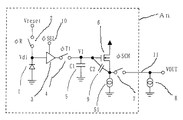
また、従来例2のイメージセンサーICの回路図を図21にタイミングチャートを図22に示す(例えば、特許文献2参照)。
フォトダイオード101のN型領域が正電源電圧端子VDDに接続しており、P型領域がリセットスイッチ102のドレインとソースフォロアアンプ103のゲートに接続している。リセットスイッチ102のソースには基準電圧VREF1が与えられている。ソースフォロアアンプ103の出力端子であるソースは、読み出しスイッチ105と定電流源104につながっている。定電流源104のゲートは基準電圧VREFAの定電圧が与えられている。図8に示す光電変換ブロックAnの枠の内側の要素は画素数分設けられており、各ブロックの読み出しスイッチ105は共通信号線106に接続している。なお、光電変換ブロックAnはnビット目の光電変換ブロックを示している。
Further, FIG. 21 shows a circuit diagram of an image sensor IC of Conventional Example 2 and FIG. 22 shows a timing chart thereof (for example, see Patent Document 2).
The N-type region of the photodiode 101 is connected to the positive power supply voltage terminal VDD, and the P-type region is connected to the drain of the reset switch 102 and the gate of the
共通信号線106は、抵抗110を通じてオペアンプ109の反転端子に入力しており、オペアンプ109の出力端子がチップセレクトスイッチ112と容量113を介して出力端子116につながっている。共通信号線106は、信号線リセットスイッチ107に接続し、信号線リセットスイッチ107のソースには基準電圧VREF2が与えられている。オペアンプ109の出力端子と反転端子の間には抵抗111が接続されていて、オペアンプ109の非反転端子は一定電圧VREF3に固定されている。オペアンプ109、抵抗110、抵抗111で反転増幅器Dが形成されている。
The common signal line 106 is input to the inverting terminal of the
イメージセンサーの出力端子116は、MOSトランジスタ114のドレインに接続し、MOSトランジスタ114のソースには基準電圧VREF4が与えられている。また、イメージセンサーの出力端子116には、寄生容量などの容量115も接続されている。容量113、容量115、MOSトランジスタ114で電圧クランプ回路Cが構成されている。
しかし、従来例1のイメージセンサーにおいては、アンプチップ200とセンサチップ100とを分離して設ける必要があるため、構成要素が多くなる欠点があった。すなわち、アンプチップは基準信号と光信号の差を増幅するが、各アンプ201、202、203のオフセットのため、センサチップに内蔵すると、センサチップ間でオフセットの差が出てしまうという問題があった。また、アンプチップの回路は、基準信号と光信号が同一の共通信号線に順に出力されるタイプのセンサチップに対応できないという問題があった。さらに増幅機能を持たせると、アンプのオフセットも増幅されてしまうという問題もあった。
However, the image sensor of Conventional Example 1 has a disadvantage that the number of components is increased because the amplifier chip 200 and the sensor chip 100 need to be provided separately. That is, the amplifier chip amplifies the difference between the reference signal and the optical signal. However, because of the offset of each
また、従来例2のイメージセンサーにおいては、VREF3の電圧と、端子106の電圧との差が大きいと反転増幅器Dの出力が、出力範囲外になり易いという問題があった。すなわち、VREF3の電圧と端子106の電圧との差が、転増幅器Dのゲイン倍で増幅されるので、反転増幅器Dのゲインが大きいと、反転増幅器Dの出力が、出力範囲外になってしまう。また、ソースフォロア回路103のオフセットはビットごとにばらつくが、VREF3の電圧は、一定であるので、全ビットの出力に対して、光電変換特性の広い直線領域を確保するのが困難であった。
Further, in the image sensor of Conventional Example 2, there is a problem that the output of the inverting amplifier D tends to be out of the output range when the difference between the voltage of VREF3 and the voltage of the terminal 106 is large. That is, the difference between the voltage at VREF3 and the voltage at the terminal 106 is amplified by the gain multiplied by the inverting amplifier D. Therefore, if the gain of the inverting amplifier D is large, the output of the inverting amplifier D is out of the output range. . Further, the offset of the
また、従来例2のメージセンサーにおいては、光電荷蓄積後、光信号を読み出してから、フォトダイオードをリセットし、その後基準信号を読み出し、光信号と基準信号の差をとるので、基準信号と光信号に乗っているリセットノイズが異なる。すなわち、異なった、タイミングのリセットノイズを比較するため、ランダムノイズが大きいという問題があった。特に、リセット電圧VREF1は、通常各イメージセンサーICの内部の基準電圧回路から供給される。このためリセット電圧には、熱雑音が含まれる。通常熱雑音は、基準電圧に大きな容量を接続することで低減することができるが、IC内部に大きな容量を設けることができないので、これらの雑音を低減することは難しい。このため、リセットする度に、フォトダイオードのリセットレベルが、揺らいでしまう。したがって、読み取りラインごとに信号レベルが変動し、読み取り画像に筋が入ってしまうという問題があった。また、各イメージセンサーICのリセット電圧が異なるので、フォトダイオードの逆バイアスがICごとに違うので、感度がICごとにばらつくという問題もあった。 Further, in the image sensor of Conventional Example 2, after the photocharge is accumulated, the optical signal is read out, then the photodiode is reset, and then the reference signal is read out, and the difference between the optical signal and the reference signal is taken. The reset noise on the signal is different. That is, there is a problem that random noise is large because different reset noises of timing are compared. In particular, the reset voltage VREF1 is normally supplied from a reference voltage circuit inside each image sensor IC. For this reason, the reset voltage includes thermal noise. Normally, thermal noise can be reduced by connecting a large capacitor to the reference voltage, but it is difficult to reduce these noises because a large capacitor cannot be provided inside the IC. For this reason, the reset level of the photodiode fluctuates every time it is reset. Therefore, there has been a problem that the signal level fluctuates for each reading line and the read image becomes streaked. Further, since the reset voltage of each image sensor IC is different, the reverse bias of the photodiode is different for each IC, so that there is a problem that the sensitivity varies for each IC.
従来のこのような問題点を解決するために、本発明は、光電変換手段に入射した光で発生した電荷の蓄積を行った後に得られる光信号と、前記光電変換手段の基準となる信号を、前半の期間と後半の期間に分けて入力し、前半の期間にサンプルし後半の期間にホールドするサンプルホールド回路と、サンプルホールド後の信号と入力される信号との差を取り出す減算器と、減算器からの信号が入力される電圧クランプ回路とを有する信号処理回路において、電圧クランプ回路は、前記前半の一部または全部の期間に第1の基準電圧にクランプすることを特徴とする信号処理回路とした。 In order to solve such conventional problems, the present invention provides an optical signal obtained after accumulating charges generated by light incident on the photoelectric conversion means and a signal serving as a reference for the photoelectric conversion means. A sample hold circuit that inputs the first half period and the second half period, samples the first half period and holds it in the second half period, and a subtractor that extracts the difference between the signal after the sample hold and the input signal; A signal processing circuit including a voltage clamp circuit to which a signal from a subtractor is input, wherein the voltage clamp circuit clamps to a first reference voltage during a part or all of the first half. A circuit was used.
この信号処理回路によれば、前半の期間と後半の期間の減算器の出力には同じオフセット電圧が乗っており、電圧クランプ回路で、この前半と後半の減算器の出力の差を取り出すので、基準電圧を基準とした、減算器のオフセットをキャンセルした信号を取り出すことができる。したがって、固定パターンノイズの小さい光電変換装置を得ることができる。 According to this signal processing circuit, the same offset voltage is on the output of the subtracter in the first half period and the second half period, and the voltage clamp circuit extracts the difference between the outputs of the first half and the second half subtractor. A signal with the offset of the subtracter canceled with respect to the reference voltage can be extracted. Therefore, a photoelectric conversion device with small fixed pattern noise can be obtained.
また、減算器の2つの入力端子に入力される信号のレベルは、1つの入力信号から分かれて作られるので、差が小さくできる。したがって、減算器のゲインが大きくても、出力の有効範囲を広くできる。 Further, since the level of the signal input to the two input terminals of the subtracter is created separately from one input signal, the difference can be reduced. Therefore, even if the gain of the subtractor is large, the effective range of output can be widened.
また、光電変換手段と信号処理回路が1つの半導体基板上に形成されたイメージセンサーICを複数実装し、各イメージセンサーICに供給する基準電圧を共通にすれば、全ての各イメージセンサーICの出力のチップ間の暗出力段差を小さくできる。 Further, if a plurality of image sensor ICs in which photoelectric conversion means and signal processing circuits are formed on one semiconductor substrate are mounted and a common reference voltage is supplied to each image sensor IC, the output of all the image sensor ICs The dark output level difference between chips can be reduced.
また、本発明は、光電変換装置と、前記光電変換装置の信号を入力する信号処理回路と、前記信号処理回路の出力に接続する信号出力端子と、前記信号処理回路に接続する基準電圧端子と、基準電圧回路と、前記基準電圧回路と前記基準電圧端子の間に設けられた抵抗とからなるイメージセンサーICとし、
前記信号処理回路は、前記光電変換装置の光電変換手段の光電変換領域に入射した光で発生した電荷の蓄積を行った後に得られる光信号と、前記光電変換手段の基準となる信号を、前半の期間と後半の期間に分けて入力し、前記入力される信号を前記前半の期間にサンプルし前記後半の期間にホールドする機能と、前記サンプルホールド後の信号と前記入力される信号との差を取り出し増幅する減算機能と、前記増幅された信号を前記前半の期間にクランプする機能とを設けた信号処理回路であり、前記クランプ機能の基準電圧は、前記基準電圧端子に接続することを特徴とした。
The present invention also provides a photoelectric conversion device, a signal processing circuit for inputting a signal of the photoelectric conversion device, a signal output terminal connected to the output of the signal processing circuit, and a reference voltage terminal connected to the signal processing circuit. An image sensor IC comprising a reference voltage circuit and a resistor provided between the reference voltage circuit and the reference voltage terminal;
The signal processing circuit includes an optical signal obtained after accumulating charges generated by light incident on a photoelectric conversion region of a photoelectric conversion unit of the photoelectric conversion device, and a signal serving as a reference for the photoelectric conversion unit in the first half And a function of sampling the input signal during the first half period and holding it during the second half period, and a difference between the signal after the sample hold and the input signal. A signal processing circuit provided with a subtraction function for extracting and amplifying the signal and a function for clamping the amplified signal during the first half period, and a reference voltage of the clamp function is connected to the reference voltage terminal. It was.
また、複数の前記イメージセンサーICの基準電圧端子を電気的に接続したことを特徴とする密着型イメージセンサーとした。 Further, the contact image sensor is characterized in that the reference voltage terminals of the plurality of image sensor ICs are electrically connected.
この信号処理回路によれば、前半の期間と後半の期間の減算器の出力には同じオフセット電圧が乗っており、電圧クランプ回路で、この前半と後半の減算器の出力の差を取り出すので、基準電圧を基準とした、減算器のオフセットをキャンセルした信号を取り出すことができる。したがって、固定パターンノイズの小さいイメージセンサーICを得ることができる。また、イメージセンサーICを複数実装し、各イメージセンサーICに供給する基準電圧を共通にしたので、全ての各イメージセンサーICの出力のチップ間の暗出力段差を小さくできる。 According to this signal processing circuit, the same offset voltage is on the output of the subtracter in the first half period and the second half period, and the voltage clamp circuit extracts the difference between the outputs of the first half and the second half subtractor. A signal with the offset of the subtracter canceled with respect to the reference voltage can be extracted. Therefore, an image sensor IC with a small fixed pattern noise can be obtained. In addition, since a plurality of image sensor ICs are mounted and the reference voltage supplied to each image sensor IC is made common, the dark output level difference between the chips of the outputs of all the image sensor ICs can be reduced.
また、この基準電圧は、各イメージセンサーIC内の基準電圧回路の発生する基準電圧の平均値となるので、外部から基準電圧を供給する必要が無い。したがって、簡単な構成で固定パターンノイズの小さい密着型イメージセンサーを供給できる。 Further, since this reference voltage is an average value of the reference voltages generated by the reference voltage circuits in each image sensor IC, it is not necessary to supply the reference voltage from the outside. Therefore, it is possible to supply a contact image sensor with a simple structure and a small fixed pattern noise.
また、本発明は、複数の光電変換手段となるフォトダイオードと、前記光電変換手段にそれぞれ接続する前期光電変換手段を初期化する複数のリセットスイッチからなるイメージセンサーICにおいて、前記複数のリセットスイッチの片方の端子が基準電圧端子に電気的に接続することを特徴とするイメージセンサーICとした。 Further, the present invention provides an image sensor IC comprising a photodiode as a plurality of photoelectric conversion means and a plurality of reset switches for initializing the photoelectric conversion means connected to the photoelectric conversion means, respectively. An image sensor IC is characterized in that one terminal is electrically connected to a reference voltage terminal.
また、前記複数の光電変換手段の出力が入力する信号処理回路を内蔵し、前記信号処理回路の基準電圧が、前記基準電圧端子に電気的に接続することを特徴とするイメージセンサーICとした。 The image sensor IC includes a signal processing circuit to which outputs of the plurality of photoelectric conversion means are input, and a reference voltage of the signal processing circuit is electrically connected to the reference voltage terminal.
また、基準電圧回路を内蔵し、前記基準電圧回路と前記基準電圧端子の間に抵抗が設けられたことを特徴とするイメージセンサーICとした。
さらに上記の、複数のイメージセンサーICの前記基準電圧端子を互いに電気的に接続したことを特徴とするイメージセンサーとした。
The image sensor IC includes a reference voltage circuit and a resistor provided between the reference voltage circuit and the reference voltage terminal.
Furthermore, the image sensor is characterized in that the reference voltage terminals of the plurality of image sensor ICs are electrically connected to each other.
このイメージセンサーによれば、全てのイメージセンサーICのフォトダイオードのリセット電圧が同じになるので、ICごとの感度のばらつきを小さくできる。また、共通にした基準電圧端子とGNDなどの間に、大きな容量を入れて、基準電圧の熱雑音を低減することで、読み取り画像に筋が入ってしまうという問題を解決できる。 According to this image sensor, since the reset voltages of the photodiodes of all the image sensor ICs are the same, variations in sensitivity among the ICs can be reduced. Further, by inserting a large capacity between the common reference voltage terminal and GND or the like to reduce the thermal noise of the reference voltage, it is possible to solve the problem of streaking in the read image.
以上説明したように、本発明は、固定パターンノイズの小さい光電変換装置が得られる。したがって、簡単な構成で、暗出力のばらつきが小さいイメージセンサーICを供給できる。
また、このイメージセンサーICを複数個直線状に実装した、密着型イメージセンサーを作製した場合、チップ間の暗出力の段差を小さくできる。
また、簡単な構成で、ICごとの感度のばらつきを小さくできる。また、読み取り画像に筋が入ってしまうという問題を解決できる。
As described above, the present invention can provide a photoelectric conversion device with a small fixed pattern noise. Therefore, it is possible to supply an image sensor IC with a simple configuration and small variations in dark output.
Further, when a contact image sensor in which a plurality of image sensor ICs are mounted in a straight line is manufactured, the step of dark output between chips can be reduced.
In addition, it is possible to reduce variations in sensitivity among ICs with a simple configuration. In addition, the problem of streaking in the read image can be solved.
以下、本発明を、図面を用いて説明する。図1は、本発明の第1の実施形態に係る信号処理回路のブロック図である。入力端子VINに入力した信号は、サンプルホールド回路21とバッファーアンプ23に入力する。サンプルホールド回路21の出力はバッファーアンプ22に入力する。バッファーアンプ22の出力とバッファーアンプ23の出力は、減算器24に入力し、減算器24の出力は電圧クランプ回路25に入力する。減算器24と電圧クランプ回路25の基準電圧は、共通にすることができVREF端子につながっている。電圧クランプ回路25の出力はバッファーアンプ26に入力する。なおバッファーアンプ26は、増幅回路に置き換えてもよい。さらに、この増幅回路の基準電圧をVREF端子と共通にしても良い。バッファーアンプ26の出力は、サンプルホールド回路27に入力する。サンプルホールド回路27の出力はバッファーアンプ28に入力する。バッファーアンプ28の出力はトランスミッションゲート29に入力する。トランスミッションゲート29の出力は出力端子VOUT2につながる。なお、トランスミッションゲート29は、用途によっては不要である。
Hereinafter, the present invention will be described with reference to the drawings. FIG. 1 is a block diagram of a signal processing circuit according to the first embodiment of the present invention. A signal input to the input terminal VIN is input to the sample hold circuit 21 and the buffer amplifier 23. The output of the sample hold circuit 21 is input to the buffer amplifier 22. The output of the buffer amplifier 22 and the output of the buffer amplifier 23 are input to the
図2は、本発明の第1の実施形態に係るサンプルホールド回路の回路図であり、サンプルホールド回路21とサンプルホールド回路27に使用できる。サンプルホールド回路はトランスミッションゲート30とダミースイッチ31と容量C1からなる。このサンプルホールド回路は、φSHとその反転であるφSHXのパルスのノイズを相殺するために、トランスミッションゲート30のNMOSとPMOSのトランジスタサイズは同じにし、ダミースイッチ31のNMOSとPMOSのトランジスタのゲート面積は、トランスミッションゲートのトランジスタのゲート面積の半分にする。
FIG. 2 is a circuit diagram of the sample and hold circuit according to the first embodiment of the present invention, and can be used for the sample and hold circuit 21 and the sample and hold
図3は、本発明の第1の実施形態に係るバッファーアンプの回路図でありオペアンプ32からなる。この回路は、バッファーアンプ22、23、26、28に使用できる。なお、バッファーアンプはソースフォロアアンプでもよい。
FIG. 3 is a circuit diagram of the buffer amplifier according to the first embodiment of the present invention, and includes an
図4は、本発明の第1の実施形態に係る増幅回路の回路図でありオペアンプ32と抵抗からなる。この回路は、バッファーアンプ26の代わりに用いれば、信号処理回路の増幅率を大きくできる。また、この増幅回路の基準電圧VREFを図1のVREF端子と共通にしても良い。
FIG. 4 is a circuit diagram of an amplifier circuit according to the first embodiment of the present invention, which includes an
図5は、本発明の第1の実施形態に係る減算器の回路図でありオペアンプ32と抵抗からなる。この回路は、INPの電圧からINMの電圧を引いた電圧を、抵抗の比率で決まるゲイン倍し、VREFの電圧を基準として出力する。INPとINMに入力する端子を逆にすれば、出力をVREFの電圧を基準に反転することができる。
FIG. 5 is a circuit diagram of the subtractor according to the first embodiment of the present invention, which includes an
図6は、本発明の第1の実施形態に係る電圧クランプ回路の回路図であり、電圧クランプ回路25に使用できる。電圧クランプ回路はトランスミッションゲート30とダミースイッチ31と容量33からなる。この電圧クランプ回路は、φCLAMPとその反転であるφCLAMPXのパルスのノイズを相殺するために、トランスミッションゲート30のNMOSとPMOSのトランジスタサイズは同じにし、ダミースイッチ31のNMOSとPMOSのトランジスタのゲート面積は、トランスミッションゲートのトランジスタのゲート面積の半分にする。
FIG. 6 is a circuit diagram of the voltage clamp circuit according to the first embodiment of the present invention, which can be used for the
図7は、本発明の第1の実施形態に係る光電変換装置の概略回路図である。図7に示す光電変換ブロックAnの枠の内側の要素は画素数分設けられており、各ブロックのチャンネル選択スイッチ7は共通信号線11に接続している。なお、光電変換ブロックAnはnビット目の光電変換ブロックを示している。図8に、本発明の第1の実施形態に係る光電変換装置の全体構成図を示す。
FIG. 7 is a schematic circuit diagram of the photoelectric conversion apparatus according to the first embodiment of the present invention. The elements inside the frame of the photoelectric conversion block An shown in FIG. 7 are provided for the number of pixels, and the channel selection switch 7 of each block is connected to the
この回路は、光電変換手段となるフォトダイオード1、電荷転送手段となる転送スイッチ4、リセット手段となるリセットスイッチ2、アンプ手段3、容量5、MOSソースフォロアを形成するMOSトランジスタ6、チャンネル選択手段となるチャンネル選択スイッチ7、共通信号線11、第1の電流源8からなる。
This circuit includes a
アンプ手段3はMOSソースフォロアやボルテージフォロアアンプ等で形成し、動作状態を選択するアンプイネーブル端子10を設けても良い。また、 MOSトランジスタ6のゲートとソース間には寄生容量9が存在する。また、MOSトランジスタ6のソースに、第2の電流源51が接続されている。この電流源はイネーブル信号φRRによってオン・オフし、オン状態では、第1の電流源8と同程度の電流が流れるようになっている。
The amplifier means 3 may be formed of a MOS source follower, a voltage follower amplifier, or the like, and may be provided with an amplifier enable terminal 10 for selecting an operation state. Further, a parasitic capacitance 9 exists between the gate and the source of the
この光電変換装置の出力端子VOUTは、図1の信号処理回路の入力端子VINに入力する。光電変換装置と信号処理回路は、1つの半導体基板上に形成することができる。
図9は、本発明の第1の実施形態に係る光電変換装置と信号処理回路のタイミングチャートである。以下にこのタイミングチャートを参照しながら、本実施形態の動作を説明する。
The output terminal VOUT of this photoelectric conversion device is input to the input terminal VIN of the signal processing circuit in FIG. The photoelectric conversion device and the signal processing circuit can be formed over one semiconductor substrate.
FIG. 9 is a timing chart of the photoelectric conversion device and the signal processing circuit according to the first embodiment of the present invention. The operation of this embodiment will be described below with reference to this timing chart.
まず、nビット目の光電変換ブロックの動作について説明する。
φR(n)によりリセットスイッチ2がオンすると、フォトダイオード1の出力端子Vdiは基準電圧Vresetに固定され、リセットスイッチ2がオフすると、Vdiの電圧はVresetにオフノイズが加算された値になる。このオフノイズは、リセットする度に電位がゆらぐので、ランダムノイズとなる。したがって、ランダムノイズを防ぐためには、リセットした後のアンプ3の出力電圧と、その後、フォトダイオードが光電荷を蓄積した後のアンプ3の出力電圧の差をとればよい。
First, the operation of the nth photoelectric conversion block will be described.
When the
そこで、図9のように、φR(n)によりリセットスイッチ2がオフした後、φT1(n)により転送スイッチ4をオンして、T Rの期間で基準信号を容量5に読み出す。このとき、イネーブル信号φRR(n)により電流源51をオン状態にすることによって、MOSトランジスタ6のソース電位を、φSCH(n)がオン状態の読み出し時と同程度にする。基準信号は、1周期の間、容量5に保持される。この間にフォトダイオード1には、光電荷が蓄積し、Vdiの電位は光電荷の量に応じて変動している。次の周期のφSCH(n)によりチャンネル選択スイッチ7をオンすると、REFの期間に、容量5に保持された基準信号が共通信号線11に読み出される。次に、φT1(n)をオンし、光信号を容量5に読み出すと、この光信号が共通信号線11に読み出される。このとき、電流源51をオフ状態にする。このことによって、TRの期間で基準信号を容量5に読み出すときと、TSの期間でフォトダイオードに蓄積した電荷に応じた光信号を容量5に読み出すときのMOSトランジスタ6のソース電位を、同程度にすることができる。したがって、容量5に蓄える電荷への寄生容量9の影響を小さくすることができる。このことによって、暗出力電圧のオフセットを小さくできる。
Therefore, as shown in FIG. 9, after the
以上の動作により、φSCH(n)のREFの期間とSIGの期間の共通信号線11の出力電圧VOUTの差を取れば、固定パターンノイズとリセットスイッチ2によるランダムノイズを除去できる。次に、φT1(n)をオフしてから、φSCH(n)をオフし、φR(n)をオンして、次回のフォトダイオードのリセットを行い、再びφT1(n)をオンして、TRの期間で基準信号を容量5に読み出す。
φSCH(n)がオフしてから、次のビットのチャンネル選択スイッチ7がφSCH(n+1)によってオンし、次のビットの基準信号の読み出しが始まる。n+1ビット目の他のパルスは、nビット目のパルスよりも、全てφSCHのオン期間だけ後ろにずれる。
By taking the difference between the output voltage VOUT of the
After φSCH (n) is turned off, the channel select switch 7 for the next bit is turned on by φSCH (n + 1), and reading of the reference signal for the next bit starts. The other pulses of the (n + 1) th bit are all shifted behind the pulse of the nth bit by the ON period of φSCH.
以上の説明で、第2の電流源51は無くてもよい。その場合は、φRRのパルスは不要となる。
In the above description, the second
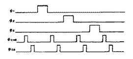
上記のように、VOUT端子からは、nビット目の基準信号、nビット目の光信号、n+1ビット目の基準信号、n+1ビット目の光信号の順で出力される。以下で、便宜上、基準信号の出力期間を前半期間、光信号の出力期間を後半期間とする。 As described above, the nth bit reference signal, the nth bit optical signal, the (n + 1) th bit reference signal, and the (n + 1) th bit optical signal are output in this order from the VOUT terminal. Hereinafter, for convenience, the output period of the reference signal is the first half period and the output period of the optical signal is the second half period.
次に信号処理回路の動作を説明する。 Next, the operation of the signal processing circuit will be described.
VIN端子に上記VOUT端子の出力が入力される。サンプルホールドパルスφSH1は、基準信号が出始めてからオンし、基準信号が終わる前にオフする。これにより、基準信号がサンプルホールドされる。VINの信号とサンプルホールド後の信号は、減算器に入力する。前半期間は同じ基準信号が減算器に入力し、後半期間は、サンプルホールドされた基準信号と光信号が減算器に入力する。したがって、減算器の出力は、前半期間はVREFレベル、後半期間は基準信号と光信号の差をゲイン倍したレベルにVREFレベルを加えたレベルにとなる。また、前半期間の出力には、バッファーアンプ22、23と減算器24のオフセットが乗り、後半期間の出力には、バッファーアンプ22、23と減算器24のオフセットと、サンプルホールド回路21のオフセットが乗る。
The output of the VOUT terminal is input to the VIN terminal. The sample hold pulse φSH1 is turned on after the reference signal starts to be output, and turned off before the reference signal ends. As a result, the reference signal is sampled and held. The VIN signal and the sample-and-hold signal are input to a subtracter. In the first half period, the same reference signal is input to the subtractor, and in the second half period, the sampled and held reference signal and the optical signal are input to the subtractor. Therefore, the output of the subtracter becomes the VREF level in the first half period, and the level obtained by adding the VREF level to the level obtained by multiplying the difference between the reference signal and the optical signal by the gain in the second half period. Further, the output of the first half period is loaded with the offsets of the buffer amplifiers 22 and 23 and the
クランプパルスφCLAMPは、φSH1がオンする前にオンし、φSH1がオフする前にオフするように加える。これにより、電圧クランプ回路25の出力は、前半期間が、VREFレベルにクランプされ、後半期間は、減算器の後半出力から前半出力を引いたレベルにVREFレベルを加えたレベルとなる。この結果、電圧クランプ回路の後半期間の出力には、バッファーアンプ22、23と減算器24のオフセットが乗らない。また、サンプルホールド回路21のオフセットは、φSHパルスとその反転であるφSHXパルスのノイズが相殺する回路になっているので小さい。以上から、電圧クランプ回路の後半期間の出力は、VREFレベルを基準に、基準信号と光信号の差をゲイン倍したレベルを加えたレベルになる。
The clamp pulse φCLAMP is applied so that it is turned on before φSH1 is turned on and turned off before φSH1 is turned off. As a result, the output of the
サンプルホールドパルスφSH2は、光信号が出始める前後にオンし、光信号が終わる前にオフする。これにより、クランプ後の出力の後半期間の出力がサンプルされ、次のビットの前半期間にホールドされる。したがって、長い期間出力レベルを維持することができる。 The sample hold pulse φSH2 is turned on before and after the optical signal starts to be output, and is turned off before the optical signal is finished. As a result, the output in the second half period of the output after clamping is sampled and held in the first half period of the next bit. Therefore, the output level can be maintained for a long period.
図10は、本発明の第2の実施形態に係る光電変換装置の概略回路図である。図10に示す光電変換ブロックAnの枠の内側の要素は画素数分設けられており、各ブロックのチャンネル選択スイッチ7は共通信号線11に接続している。なお、光電変換ブロックAnはnビット目の光電変換ブロックを示している。図8に、光電変換装置の全体構成図を示し、本発明の第1の実施形態と同様である。
FIG. 10 is a schematic circuit diagram of a photoelectric conversion apparatus according to the second embodiment of the present invention. The elements inside the frame of the photoelectric conversion block An shown in FIG. 10 are provided for the number of pixels, and the channel selection switch 7 of each block is connected to the
この回路は、光電変換手段となるフォトダイオード1、電荷転送手段となる転送スイッチ14、15、16、17、リセット手段となるリセットスイッチ2、アンプ手段3、光信号を保持する容量13、光電変換手段の基準となる基準信号を保持する容量12、信号読み出し手段となるMOSソースフォロアを形成するMOSトランジスタ6、チャンネル選択手段となるチャンネル選択スイッチ7、共通信号線11、第1の電流源8からなる。
アンプ手段3はMOSソースフォロアやボルテージフォロアアンプ等で形成し、動作状態を選択するアンプイネーブル端子10を設けても良い。
This circuit includes a
The amplifier means 3 may be formed of a MOS source follower, a voltage follower amplifier, or the like, and may be provided with an amplifier enable terminal 10 for selecting an operation state.
この光電変換装置の出力端子VOUTは、図1の信号処理回路の入力端子VINに入力する。光電変換装置と信号処理回路は、1つの半導体基板上に形成することができる。
図11は、本発明の実施形態例の光電変換装置2と信号処理回路のタイミングチャートである。
The output terminal VOUT of this photoelectric conversion device is input to the input terminal VIN of the signal processing circuit in FIG. The photoelectric conversion device and the signal processing circuit can be formed over one semiconductor substrate.
FIG. 11 is a timing chart of the
以下にこのタイミングチャートを参照しながら、光電変換装置の動作を説明する。
図11のφR、φRIN、φSIN、φSELは全ビットについて同時に動作する。φSO、φRO、φSCHはビットによって動作するタイミングが異なるので、(n)付で表示している。
The operation of the photoelectric conversion device will be described below with reference to this timing chart.
In FIG. 11, φR, φRIN, φSIN, and φSEL operate simultaneously for all bits. Since φSO, φRO, and φSCH operate at different bits, they are indicated with (n).
まず、nビット目の光電変換ブロックの動作について説明する。φSINのS1の位置のパルスにより転送スイッチ15をオンして、フォトダイオード1に入射した光で発生した電荷の蓄積を行った後に得られる光信号を容量13に読み出す。次にφRのR2の位置のパルスによりリセットスイッチ2がオンすると、フォトダイオード1の出力端子Vdiは基準電圧Vresetに固定され、リセットスイッチ2がオフすると、Vdiの電圧はVresetにオフノイズが加算された値になる。次にリセットスイッチ2がオフした直後、φRINのR2の位置のパルスにより転送スイッチ14をオンして、フォトダイオード1のリセット後の基準信号を容量12に読み出す。この後フォトダイオード1には、光電荷が蓄積し、Vdiの電位は光電荷の量に応じて変動する。この蓄積期間はφRのR2の期間の終了から、次の周期のφSINのS2の期間の終了までであるので、図11のTS2の期間となり、全てのビットについて同じ期間になる。
First, the operation of the nth photoelectric conversion block will be described. The
次に、基準信号と光信号の読み出しの動作を説明する。
図11のTS2の蓄積期間中に、φSCH(n)のパルスによりチャンネル選択スイッチ7をオンすると同時にφSO(n)のパルスにより転送スイッチ17をオンすると、容量13に保持されていた光信号が共通信号線11に読み出される。この期間はφSCH(n)のS1の部分である。この光信号は、TS1の期間に蓄積された信号である。次に、φRO(n)のパルスにより転送スイッチ16をオンすると、容量12に保持されていた基準信号が共通信号線11に読み出される。この基準信号は、φRのR2の位置のパルスによりリセットされた信号である。
Next, the reading operation of the reference signal and the optical signal will be described.
When the channel selection switch 7 is turned on by the pulse of φSCH (n) and the
次に、φSCH(n)をオフしてから、次のビットのチャンネル選択スイッチ7がφSCH(n+1)によってオンし、φSO(n+1)のパルスにより次のビットの転送スイッチ17をオンすると次のビットの光信号の読み出しが始まる。n+1ビット目の他のパルスは、nビット目のパルスよりも、全てφSCHのオン期間だけ後ろにずれる。
Next, after turning off φSCH (n), the channel selection switch 7 of the next bit is turned on by φSCH (n + 1), and the
この実施例では、TS2の期間でフォトダイオードが蓄積動作中に、前の蓄積期間TS1の期間で蓄積した光信号を読み出すことができる。したがって、RGBの3色のLEDを順に点灯して、カラー画像データを読み取ることができる。たとえば、TS1の期間に赤のLEDを点灯し赤の成分を読み取り、TS2の期間に緑のLEDを点灯し緑の成分を読み取り、TS2の次の期間に青のLEDを点灯し青の成分を読み取ることができる。この場合、TS2の期間内に赤の光信号を読み出すことになる。 In this embodiment, the optical signal accumulated in the previous accumulation period TS1 can be read out while the photodiode is accumulating in the period TS2. Therefore, the color image data can be read by sequentially turning on LEDs of three colors RGB. For example, the red LED is lit and the red component is read during the period of TS1, the green LED is lit and the green component is read during the period of TS2, the blue LED is lit and the blue component is read during the next period of TS2. Can be read. In this case, a red light signal is read out within the period TS2.
上記のように、共通信号線11のVOUT端子からは、nビット目の光信号、nビット目の基準信号、n+1ビット目の光信号、n+1ビット目の基準信号の順で出力される。これは、光電変換装置1と光信号と基準信号の順番が逆になるが、図11に示すパルスφSH1、φCLAMP、φSH2を使い、本発明の第1の実施形態に係る光電変換装置と同様に、図1の信号処理回路で光信号と基準信号の差をVREFを基準に増幅することができる。
As described above, from the VOUT terminal of the
以上の説明で、光電変換装置は、基準信号と光信号を順に出力するものであれば、どのような回路であってもよい。リニアセンサー、エリアセンサーともに信号処理することができる。また、基準信号と光信号の出力の順が逆であっても、減算器のINPとINMの端子を逆に接続すれば、対応できる。また、減算器のIMPとINMの端子を逆に接続すれば、減算器の出力はVREFレベルを基準に反転するので、光信号の感度が正負どちらであっても、信号処理回路の感度を正にできる。 In the above description, the photoelectric conversion device may be any circuit as long as it sequentially outputs the reference signal and the optical signal. Both linear and area sensors can process signals. Further, even if the output order of the reference signal and the optical signal is reversed, it can be handled by connecting the INP and INM terminals of the subtractor in reverse. If the IMP and INM terminals of the subtractor are connected in reverse, the output of the subtracter is inverted with respect to the VREF level, so that the sensitivity of the signal processing circuit is positive regardless of whether the sensitivity of the optical signal is positive or negative. Can be.
以上のように、本発明によれば、前半の期間と後半の期間の減算器の出力には同じオフセット電圧が乗っており、電圧クランプ回路で、この前半と後半の減算器の出力の差を取り出すので、基準電圧を基準とした、減算器のオフセットをキャンセルした信号を取り出すことができる。したがって、固定パターンノイズの小さい電変換装置を得ることができる。また、光電変換手段と信号処理回路が1つの半導体基板上に形成されたリニアイメージセンサーICやエリアイメージセンサーICを作ることができる。また、このリニアイメージセンサーICを複数実装し、各イメージセンサーICに供給する基準電圧を共通にすれば、全ての各イメージセンサーICの出力のチップ間の暗出力段差を小さくできる。このとき、信号処理回路には、トランスミッションゲート29が設けられているので、各イメージセンサーICの出力を共通の信号線に読み出すことが可能である。
As described above, according to the present invention, the same offset voltage is on the output of the subtracter in the first half period and the second half period, and the difference between the output of the first half and the second half subtractor is calculated by the voltage clamp circuit. Since it is extracted, it is possible to extract a signal in which the offset of the subtracter is canceled with reference to the reference voltage. Therefore, an electric conversion device with a small fixed pattern noise can be obtained. Further, a linear image sensor IC or an area image sensor IC in which the photoelectric conversion means and the signal processing circuit are formed on one semiconductor substrate can be manufactured. Further, if a plurality of linear image sensor ICs are mounted and a common reference voltage is supplied to each image sensor IC, the dark output level difference between chips of all the image sensor IC outputs can be reduced. At this time, since the
図12は、本発明の第3の実施形態に係る密着型イメージセンサーの概略図である。この密着型イメージセンサーは3つのイメージセンサーIC41からなり、それぞれのイメージセンサーIC41は、信号処理回路42、光電変換装置43、基準電圧回路44、抵抗45、基準電圧端子46、信号出力端子47からなる。光電変換装置43の共通信号線は、信号処理回路42に入力し、信号処理回路42の出力は信号出力端子47につながっている。また、基準電圧端子46は、信号処理回路42の基準電圧につながっており、基準電圧回路44と基準電圧端子46の間に抵抗45が設けてある。
FIG. 12 is a schematic view of a contact image sensor according to the third embodiment of the present invention. The contact image sensor includes three
全てのイメージセンサーIC41の信号出力端子47は、外部で接続されており、VOUT2端子から外部に出力される。全てのイメージセンサーIC41の基準電圧端子46も外部で接続されており、必要に応じて、基準電圧端子46とGND間に、基準電圧VREFを安定にするための容量48が設けてある。
The
それぞれのイメージセンサーIC41の基準電圧回路44の出力電圧は、プロセスばらつき等によってばらつく。しかし、この出力電圧は抵抗45を介して、互いにショートしているので、容量48のVREF電位は、3チップの基準電圧回路44の出力電圧の平均値となる。この電圧VREFが、全てのイメージセンサーIC41の信号処理回路42に供給されることになる。
The output voltage of the
なお、信号処理回路42は、図1の信号処理回路を用いることができ、光電変換装置43は、図7または図10の光電変換装置を用いることができる。信号処理回路42と光電変換装置43の動作は、実施例1と実施例2で述べたとおりである。
The
以上のように、本発明によれば、前半の期間と後半の期間の減算器の出力には同じオフセット電圧が乗っており、電圧クランプ回路でこの前半と後半の減算器の出力の差を取り出すので、基準電圧を基準とした、減算器のオフセットをキャンセルした信号を取り出すことができる。
そして、電圧クランプ回路に供給される基準電圧は、全てのイメージセンサーICについて同じレベルであるので、全てのイメージセンサーICの出力のチップ間の暗出力段差を小さくできる。すなわち固定パターンノイズの小さい密着型イメージセンサーを得ることができる。このとき、信号処理回路には、トランスミッションゲート29が設けられているので、各イメージセンサーICの出力を共通の信号線に読み出すことが可能である。
As described above, according to the present invention, the same offset voltage is put on the output of the subtracter in the first half period and the second half period, and the difference between the outputs of the first half and the second half subtractor is taken out by the voltage clamp circuit. Therefore, it is possible to take out a signal in which the offset of the subtracter is canceled with reference to the reference voltage.
Since the reference voltage supplied to the voltage clamp circuit is at the same level for all the image sensor ICs, the dark output step between the chips of the outputs of all the image sensor ICs can be reduced. That is, a contact image sensor with a small fixed pattern noise can be obtained. At this time, since the
図13は、本発明の第4の実施形態に係る密着型イメージセンサーの概略図である。この密着型イメージセンサーは3つのイメージセンサーIC41からなり、それぞれのイメージセンサーIC41は、信号処理回路42、光電変換装置43、基準電圧端子46、信号出力端子47からなる。光電変換装置43の共通信号線は、信号処理回路42に入力し、信号処理回路42の出力は信号出力端子47につながっている。
FIG. 13 is a schematic view of a contact image sensor according to the fourth embodiment of the present invention. The contact image sensor includes three
全てのイメージセンサーIC41の信号出力端子47は、外部で接続されており、VOUT2端子から外部に出力される。全てのイメージセンサーIC41の基準電圧端子46も外部で接続されており、必要に応じて、基準電圧端子46とGND間に、基準電圧VREFを安定にするための容量48が設けてある。この電圧VREFが、全てのイメージセンサーIC41の光電変換装置43のVreset端子に供給されている。
信号処理回路42は、図1の信号処理回路を用いることができる。
The
As the
図14は、本発明の第4の実施形態に係る光電変換装置の概略回路図であり、図10に示した光電変換装置との相違は、Vreset端子が光電変換装置の領域外に設けている点である。図14に示す光電変換ブロックAnの枠の内側の要素は画素数分設けられており、各ブロックのチャンネル選択スイッチ7は共通信号線11に接続している。なお、光電変換ブロックAnはnビット目の光電変換ブロックを示している。
図15に、本発明の第4の実施形態に係る光電変換装置の全体構成図を示す。
この回路は、光電変換手段となるフォトダイオード1、電荷転送手段となる転送スイッチ14、15、16、17、リセット手段となるリセットスイッチ2、アンプ手段3、光信号を保持する容量13、光電変換手段の基準となる基準信号を保持する容量12、信号読み出し手段となるMOSソースフォロアを形成するMOSトランジスタ6、チャンネル選択手段となるチャンネル選択スイッチ7、共通信号線11、第1の電流源8からなる。
リセットスイッチ2の片方の端子は、Vreset端子につながっており、図15に示すように全ての光電変換装置のVreset端子は共通である。
FIG. 14 is a schematic circuit diagram of a photoelectric conversion device according to the fourth embodiment of the present invention. The difference from the photoelectric conversion device shown in FIG. 10 is that the Vreset terminal is provided outside the region of the photoelectric conversion device. Is a point. The elements inside the frame of the photoelectric conversion block An shown in FIG. 14 are provided for the number of pixels, and the channel selection switch 7 of each block is connected to the
FIG. 15 is an overall configuration diagram of a photoelectric conversion apparatus according to the fourth embodiment of the present invention.
This circuit includes a
One terminal of the
アンプ手段3はMOSソースフォロアやボルテージフォロアアンプ等で形成し、動作状態を選択するアンプイネーブル端子10を設けても良い。
この光電変換装置の出力端子VOUTは、図1の信号処理回路の入力端子VINに入力する。光電変換装置と信号処理回路は、1つの半導体基板上に形成することができる。
図16は、本発明の第4の実施形態に係る光電変換装置と信号処理回路のタイミングチャートである。
The amplifier means 3 may be formed of a MOS source follower, a voltage follower amplifier, or the like, and may be provided with an amplifier enable terminal 10 for selecting an operation state.
The output terminal VOUT of this photoelectric conversion device is input to the input terminal VIN of the signal processing circuit in FIG. The photoelectric conversion device and the signal processing circuit can be formed over one semiconductor substrate.
FIG. 16 is a timing chart of the photoelectric conversion device and the signal processing circuit according to the fourth embodiment of the present invention.
以下にこのタイミングチャートを参照しながら、光電変換装置の動作を説明する。
図16のφR、φRIN、φSIN、φSELは全ビットについて同時に動作する。φSO、φRO、φSCHはビットによって動作するタイミングが異なるので、(n)付で表示している。
まず、nビット目の光電変換ブロックの動作について説明する。
φSINのS1の位置のパルスにより転送スイッチ15をオンして、フォトダイオード1に入射した光で発生した電荷の蓄積を行った後に得られる光信号を容量13に読み出す。次にφRのR2の位置のパルスによりリセットスイッチ2がオンすると、フォトダイオード1の出力端子Vdiは基準電圧Vresetに固定され、リセットスイッチ2がオフすると、Vdiの電圧はVresetにオフノイズが加算された値になる。ここで、Vresetは、図13に示すようにVREFと等しく、熱雑音が小さいので、Vdiの電圧は、リセットする度に変動する量が小さくなる。
The operation of the photoelectric conversion device will be described below with reference to this timing chart.
In FIG. 16, φR, φRIN, φSIN, and φSEL operate simultaneously for all bits. Since φSO, φRO, and φSCH operate at different bits, they are indicated with (n).
First, the operation of the nth photoelectric conversion block will be described.
The
次にリセットスイッチ2がオフした直後、φRINのR2の位置のパルスにより転送スイッチ14をオンして、フォトダイオード1のリセット後の基準信号を容量12に読み出す。この後フォトダイオード1には、光電荷が蓄積し、Vdiの電位は光電荷の量に応じて変動する。この蓄積期間はφRのR2の期間の終了から、次の周期のφSINのS2の期間の終了までであるので、図6のTS2の期間となり、全てのビットについて同じ期間になる。
次に、基準信号と光信号の読み出しの動作を説明する。
Next, immediately after the
Next, the reading operation of the reference signal and the optical signal will be described.
図16のTS2の蓄積期間中に、φSCH(n)のパルスによりチャンネル選択スイッチ7をオンすると同時にφSO(n)のパルスにより転送スイッチ17をオンすると、容量13に保持されていた光信号が共通信号線11に読み出される。この期間はφSCH(n)のS1の部分である。
この光信号は、TS1の期間に蓄積された信号であり、φRのR1の位置のパルスによりリセットされたリセット電圧を基準としている。
When the channel selection switch 7 is turned on by the pulse of φSCH (n) and the
This optical signal is a signal accumulated during the period TS1, and is based on the reset voltage reset by the pulse at the R1 position of φR.
次に、φRO(n)のパルスにより転送スイッチ16をオンすると、容量12に保持されていた基準信号が共通信号線11に読み出される。この基準信号は、φRのR2の位置のパルスによりリセットされた信号である。
後段の信号処理回路で、この光信号と基準信号の差を取ると、φRの異なるパルスのリセットレベルの差を取ることになるが、Vreset電圧の熱雑音が小さいので、光による電圧差だけを取り出すことができる。
次に、φSCH(n)をオフしてから、次のビットのチャンネル選択スイッチ7がφSCH(n+1)によってオンし、φSO(n+1)のパルスにより次のビットの転送スイッチ17をオンすると次のビットの光信号の読み出しが始まる。n+1ビット目の他のパルスは、nビット目のパルスよりも、全てφSCHのオン期間だけ後ろにずれる。
Next, when the
If the difference between this optical signal and the reference signal is taken in the signal processing circuit in the subsequent stage, the difference in the reset level of the pulses having different φR will be taken. However, since the thermal noise of the Vreset voltage is small, only the voltage difference due to light is taken. It can be taken out.
Next, after turning off φSCH (n), the channel selection switch 7 of the next bit is turned on by φSCH (n + 1), and the
この実施例では、TS2の期間でフォトダイオードが蓄積動作中に、前の蓄積期間TS1の期間で蓄積した光信号を読み出すことができる。したがって、RGBの3色のLEDを順に点灯して、カラー画像データを読み取ることができる。たとえば、TS1の期間に赤のLEDを点灯し赤の成分を読み取り、TS2の期間に緑のLEDを点灯し緑の成分を読み取り、TS2の次の期間に青のLEDを点灯し青の成分を読み取ることができる。この場合、TS2の期間内に赤の光信号を読み出すことになる。 In this embodiment, the optical signal accumulated in the previous accumulation period TS1 can be read out while the photodiode is accumulating in the period TS2. Therefore, the color image data can be read by sequentially turning on LEDs of three colors RGB. For example, the red LED is lit and the red component is read during the period of TS1, the green LED is lit and the green component is read during the period of TS2, the blue LED is lit and the blue component is read during the next period of TS2. Can be read. In this case, a red light signal is read out within the period TS2.
上記のように、共通信号線11のVOUT端子からは、nビット目の光信号、nビット目の基準信号、n+1ビット目の光信号、n+1ビット目の基準信号の順で出力される。これは、光電変換装置1と光信号と基準信号の順番が逆になるが、図16に示すパルスφSH1、φCLAMP、φSH2を使い、本発明の第1の実施形態に係る光電変換装置と同様に、図1の信号処理回路で光信号と基準信号の差をVREFを基準に増幅することができる。
As described above, from the VOUT terminal of the
以上の説明で、光電変換装置は、基準信号と光信号を順に出力するものであれば、どのような回路であってもよい。リニアセンサー、エリアセンサーともに信号処理することができる。また、基準信号と光信号の出力の順が逆であっても、減算器のINPとINMの端子を逆に接続すれば、対応できる。また、減算器のIMPとINMの端子を逆に接続すれば、減算器の出力はVREFレベルを基準に反転するので、光信号の感度が正負どちらであっても、信号処理回路の感度を正にできる。 In the above description, the photoelectric conversion device may be any circuit as long as it sequentially outputs the reference signal and the optical signal. Both linear and area sensors can process signals. Further, even if the output order of the reference signal and the optical signal is reversed, it can be handled by connecting the INP and INM terminals of the subtractor in reverse. If the IMP and INM terminals of the subtractor are connected in reverse, the output of the subtracter is inverted with respect to the VREF level, so that the sensitivity of the signal processing circuit is positive regardless of whether the sensitivity of the optical signal is positive or negative. Can be.
以上のように、本発明によれば、前半の期間と後半の期間の減算器の出力には同じオフセット電圧が乗っており、電圧クランプ回路で、この前半と後半の減算器の出力の差を取り出すので、基準電圧を基準とした、減算器のオフセットをキャンセルした信号を取り出すことができる。したがって、固定パターンノイズの小さい電変換装置を得ることができる。また、光電変換手段と信号処理回路が1つの半導体基板上に形成されたリニアイメージセンサーICやエリアイメージセンサーICを作ることができる。 As described above, according to the present invention, the same offset voltage is on the output of the subtracter in the first half period and the second half period, and the difference between the output of the first half and the second half subtractor is calculated by the voltage clamp circuit. Since it is extracted, it is possible to extract a signal in which the offset of the subtracter is canceled with reference to the reference voltage. Therefore, an electric conversion device with a small fixed pattern noise can be obtained. Further, a linear image sensor IC or an area image sensor IC in which the photoelectric conversion means and the signal processing circuit are formed on one semiconductor substrate can be manufactured.
また、図13に示すように、このリニアイメージセンサーICを複数実装し、各イメージセンサーICに供給するリセット電圧を共通にすれば、全てのイメージセンサーICのフォトダイオードのリセット電圧が同じになるので、ICごとの感度のばらつきを小さくできる。また、この実施例によれば、受光素子のリセット電圧を、VREF端子を通じて外部から供給できるので、熱雑音の小さい安定した電圧を供給することができる、したがって、読み取り画像に筋が入ってしまうという問題を解決できる。 As shown in FIG. 13, if a plurality of linear image sensor ICs are mounted and the reset voltage supplied to each image sensor IC is made common, the reset voltages of the photodiodes of all the image sensor ICs are the same. , Variation in sensitivity between ICs can be reduced. In addition, according to this embodiment, the reset voltage of the light receiving element can be supplied from the outside through the VREF terminal, so that a stable voltage with small thermal noise can be supplied. Can solve the problem.
また、共通にした基準電圧端子とGNDなどの間に、大きな容量48を入れて、リセット電圧の熱雑音をさらに低減することで、より安定した読み取り画像を得ることができる。
容量48は0.01uF以上とし、VREF端子より供給するリセット電圧は1Vから、電源電圧よりも1V程度低い電圧の範囲とするとよい。
以上の本発明の実施形4の密着型イメージセンサーの説明で、信号処理回路42は、ICに内蔵されていなくともよい。
Further, by inserting a
The
In the above description of the contact image sensor according to the fourth embodiment of the present invention, the
図17は、本発明の第5の実施形態に係る密着型イメージセンサーの概略図である。第4の実施形態例との違いは、信号処理回路42の基準電圧VREFを、受光素子のリセット電圧と共通にしたことである。このとき、受光素子のリセット電圧は、自由に設定できなくなるが、信号処理回路42の基準電圧VREFは通常1V前後であるので、実用上問題ない。
FIG. 17 is a schematic view of a contact image sensor according to the fifth embodiment of the present invention. The difference from the fourth embodiment is that the reference voltage VREF of the
これにより、ICの外部から供給する基準電圧を1種類にすることができ、また、信号処理回路42の基準電圧の安定性と熱雑音も小さくできるので、信号処理回路42で乗る雑音も小さくすることができる。
As a result, the reference voltage supplied from the outside of the IC can be made one type, and the stability of the reference voltage of the
図18は、本発明の第6の実施形態に係る密着型イメージセンサーの概略図である。第4の実施形態例との違いは、各イメージセンサーIC41の内部に、基準電圧回路44と、基準電圧回路44の出力端子と基準電圧端子46の間の抵抗45が設けてある点である。抵抗45の値は1KΩ前後とする。
FIG. 18 is a schematic view of a contact image sensor according to the sixth embodiment of the present invention. The difference from the fourth embodiment is that a
図18の構成のイメージセンサーでは、基準電圧VREFは、各イメージセンサーIC41の内部の基準電圧回路44の発生する基準電圧の平均値になる。したがって、全てのイメージセンサーIC41のリセット電圧は、同一にすることができ、本発明の第4の実施形態例の密着型イメージセンサーと同じ効果が得られる。さらに、外部から基準電圧を供給する必要が無く、使いやすい。
In the image sensor having the configuration shown in FIG. 18, the reference voltage VREF is an average value of the reference voltages generated by the
また、図示していないが、図18の構成で、信号処理回路42の基準電圧VREFを、受光素子のリセット電圧と共通にすることもできる。この場合、本発明の第5の実施形態例の密着型イメージセンサーと同じ効果が得られる。さらに、外部から基準電圧を供給する必要が無く、使いやすい。
以上の説明で、本発明は上述した各実施形態に限定されるものではなく、その要旨を逸脱しない範囲で、種々変形して実施することができる。
Although not shown, the reference voltage VREF of the
In the above description, the present invention is not limited to the above-described embodiments, and various modifications can be made without departing from the scope of the invention.
1 フォトダイオード
2 リセットスイッチ
3 アンプ
4 転送スイッチ
5 容量
6 MOSトランジスタ
7 チャンネル選択スイッチ
8 第1の電流源
9 寄生容量
10 アンプイネーブル端子
11 共通信号線
12、13 容量
14、15、16、17 転送スイッチ
21 サンプルホールド回路
22 バッファーアンプ
23 バッファーアンプ
24 減算器
25 電圧クランプ回路
26 バッファーアンプ
27 サンプルホールド回路
28 バッファーアンプ
29 トランスミッションゲート
30 トランスミッションゲート
31 ダミースイッチ
32 オペアンプ
33 クランプ容量
41 イメージセンサーIC
42 信号処理回路
43 光電変換装置
44 基準電圧回路
45 抵抗
46 基準電圧端子
47 信号出力端子
48 容量
51 第2の電流源
An nビット目の光電変換ブロック
101 フォトダイオード
102 リセットスイッチ
103 ソースフォロアアンプ
104 定電流源
105 読み出しスイッチ
106 共通信号線
107 信号線リセットスイッチ
108 寄生容量
109 オペアンプ
110 抵抗
111 抵抗
112 チップセレクトスイッチ
113 容量
114 MOSトランジスタ
115 容量
116 出力端子
An nビット目の光電変換ブロック
Bm mチップ目のイメージセンサーICブロック
C クランプ回路
D 反転増幅器
1
4
DESCRIPTION OF
42
102
D inverting amplifier
Claims (19)
前記サンプルホールド後の信号と前記入力される信号との差を取り出す減算器と、
前記減算器からの信号が入力される電圧クランプ回路と、を有する信号処理回路において、
前記電圧クランプ回路は、前記前半の一部または全部の期間にクランプすることを特徴とする信号処理回路。 A sample-and-hold circuit that samples input signals divided into the first half period and the second half period and holds them in the first half period; and
A subtractor for extracting a difference between the signal after the sample hold and the input signal;
In a signal processing circuit having a voltage clamp circuit to which a signal from the subtractor is input,
The signal processing circuit according to claim 1, wherein the voltage clamp circuit clamps a part or all of the first half period.
前記前半の期間に前記光信号を入力し、前記後半の期間に前記基準信号を入力する、または、前記前半の期間に前記基準信号を入力し、前記後半の期間に前記光信号を入力することを特徴とする請求項1記載の信号処理回路。 The signal processing circuit is a signal processing circuit for inputting an optical signal obtained after accumulating charges generated by light incident on the photoelectric conversion means and a reference signal serving as a reference for the photoelectric conversion means,
The optical signal is input during the first half period and the reference signal is input during the second half period, or the reference signal is input during the first half period and the optical signal is input during the second half period. The signal processing circuit according to claim 1.
前記共通信号線からの信号が入力されるサンプルホールド回路と、
前記サンプルホールド後の信号と前記入力される信号との差を取り出し増幅する減算器と、を有することを特徴とするイメージセンサー。 An optical signal obtained after accumulating charges generated by light incident on the photoelectric conversion means, and a reading means for sequentially reading out a reference signal serving as a reference for the photoelectric conversion means to a common signal line;
A sample hold circuit to which a signal from the common signal line is input;
An image sensor comprising: a subtracter that extracts and amplifies a difference between the signal after the sample hold and the input signal.
前記光電変換手段の基準となる基準信号を保持する第2の保持手段と、
前記保持された光信号と前記基準信号とを順に共通信号線に読み出す読み出し手段と、
前記共通信号線からの信号が入力されるサンプルホールド回路と、
前記サンプルホールド後の信号と前記入力される信号との差を取り出し増幅する減算器と、を有することを特徴とするイメージセンサー。 First holding means for holding an optical signal obtained after accumulating charges generated by light incident on the photoelectric conversion means;
Second holding means for holding a reference signal which is a reference of the photoelectric conversion means;
Read means for sequentially reading the held optical signal and the reference signal to a common signal line;
A sample hold circuit to which a signal from the common signal line is input;
An image sensor comprising: a subtracter that extracts and amplifies a difference between the signal after the sample hold and the input signal.
前記光電変換装置の信号を入力する信号処理回路と、
前記信号処理回路の出力に接続する信号出力端子と、
前記信号処理回路の基準電圧に接続する基準電圧端子と、
基準電圧回路と、
前記基準電圧回路と前記基準電圧端子の間に設けられた抵抗と、を有し、
前記信号処理回路は、前記光電変換装置の光電変換手段の光電変換領域に入射した光で発生した電荷の蓄積を行った後に得られる光信号と、前記光電変換手段の基準となる信号を、前半の期間と後半の期間に分けて入力し、前記入力される信号を前記前半の期間にサンプルし前記後半の期間にホールドするサンプルホールド回路と、前記サンプルホールド後の信号と前記入力される信号との差を取り出す減算器と、前記減算器からの信号を前記前半の期間にクランプするクランプ回路と、を有し、
前記電圧クランプ回路の基準電圧または前記減算器の基準電圧が、前記基準電圧端子により与えられることを特徴とするイメージセンサーIC。 A photoelectric conversion device;
A signal processing circuit for inputting a signal of the photoelectric conversion device;
A signal output terminal connected to the output of the signal processing circuit;
A reference voltage terminal connected to a reference voltage of the signal processing circuit;
A reference voltage circuit;
A resistor provided between the reference voltage circuit and the reference voltage terminal;
The signal processing circuit includes an optical signal obtained after accumulating charges generated by light incident on a photoelectric conversion region of a photoelectric conversion unit of the photoelectric conversion device, and a signal serving as a reference for the photoelectric conversion unit in the first half A sample-and-hold circuit that inputs the input signal divided into the first half period and the second half period, samples the input signal in the first half period and holds the sampled signal in the second half period, and the signal after the sample hold and the input signal A subtractor that extracts the difference between the subtractor, and a clamp circuit that clamps the signal from the subtractor in the first half period,
An image sensor IC, wherein a reference voltage of the voltage clamp circuit or a reference voltage of the subtracter is given by the reference voltage terminal.
前記光電変換手段にそれぞれ接続する前期光電変換手段を初期化する複数のリセットスイッチと、からなるイメージセンサーICにおいて、
前記複数のリセットスイッチは基準電圧端子に電気的に接続することを特徴とするイメージセンサーIC。 A plurality of photoelectric conversion means;
In an image sensor IC comprising a plurality of reset switches for initializing the photoelectric conversion means connected to the photoelectric conversion means respectively,
The image sensor IC, wherein the plurality of reset switches are electrically connected to a reference voltage terminal.
前記光電変換手段にそれぞれ接続する前期光電変換手段を初期化する複数のリセットスイッチと、
光電変換手段に入射した光で発生した電荷の蓄積を行った後に得られる光信号を保持する第1の保持手段と、
前記光電変換手段の基準となる基準信号を保持する第2の保持手段と、
前記保持された光信号と基準信号を順に共通信号線に読み出す読み出し手段と、
からなるイメージセンサーICにおいて、
前記複数のリセットスイッチが基準電圧端子に電気的に接続することを特徴とするイメージセンサーIC。 A plurality of photoelectric conversion means;
A plurality of reset switches for initializing the photoelectric conversion means connected to the photoelectric conversion means,
First holding means for holding an optical signal obtained after accumulating charges generated by light incident on the photoelectric conversion means;
Second holding means for holding a reference signal which is a reference of the photoelectric conversion means;
Read means for sequentially reading the held optical signal and reference signal to a common signal line;
In the image sensor IC consisting of
The image sensor IC, wherein the plurality of reset switches are electrically connected to a reference voltage terminal.
前記サンプルホールド回路は前記入力信号の前半期間において前記入力信号を保持して前記減算器へ出力し、前記減算器は前記後半期間において前記サンプルホールド回路からの信号と前記入力信号との差信号を前記クランプ回路に出力し、前記電圧クランプ回路は前記前半期間に前記電圧クランプ回路の出力を前記基準電圧にクランプし、次に、前記後半期間に前記基準電圧に前記差信号を重畳させることを特徴とする信号処理方法。 A sample hold circuit for inputting an input signal having at least a first half period and a second half period, a subtracter for inputting a signal from the sample hold circuit and the input signal, a signal from the subtractor, and a reference voltage are input. In a signal processing method of a signal processing circuit having a voltage clamp circuit to perform,
The sample hold circuit holds the input signal in the first half period of the input signal and outputs it to the subtracter, and the subtracter outputs a difference signal between the signal from the sample hold circuit and the input signal in the second half period. Output to the clamp circuit, the voltage clamp circuit clamps the output of the voltage clamp circuit to the reference voltage in the first half period, and then superimposes the difference signal on the reference voltage in the second half period. A signal processing method.
Priority Applications (3)
| Application Number | Priority Date | Filing Date | Title |
|---|---|---|---|
| JP2004023097A JP2005012752A (en) | 2003-02-26 | 2004-01-30 | Signal processing circuit, image sensor ic, and signal processing method |
| US10/784,494 US7189953B2 (en) | 2003-02-26 | 2004-02-23 | Signal processing circuit, image sensor IC, and signal processing method |
| CNB2004100684958A CN100484182C (en) | 2003-02-26 | 2004-02-26 | Signal processing circuit, image sensor IC and signal processing method |
Applications Claiming Priority (4)
| Application Number | Priority Date | Filing Date | Title |
|---|---|---|---|
| JP2003049573 | 2003-02-26 | ||
| JP2003049574 | 2003-02-26 | ||
| JP2003149268 | 2003-05-27 | ||
| JP2004023097A JP2005012752A (en) | 2003-02-26 | 2004-01-30 | Signal processing circuit, image sensor ic, and signal processing method |
Publications (2)
| Publication Number | Publication Date |
|---|---|
| JP2005012752A true JP2005012752A (en) | 2005-01-13 |
| JP2005012752A5 JP2005012752A5 (en) | 2007-02-15 |
Family
ID=33102323
Family Applications (1)
| Application Number | Title | Priority Date | Filing Date |
|---|---|---|---|
| JP2004023097A Withdrawn JP2005012752A (en) | 2003-02-26 | 2004-01-30 | Signal processing circuit, image sensor ic, and signal processing method |
Country Status (3)
| Country | Link |
|---|---|
| US (1) | US7189953B2 (en) |
| JP (1) | JP2005012752A (en) |
| CN (1) | CN100484182C (en) |
Cited By (8)
| Publication number | Priority date | Publication date | Assignee | Title |
|---|---|---|---|---|
| WO2007010854A1 (en) * | 2005-07-22 | 2007-01-25 | Rohm Co., Ltd. | Semiconductor device, module and electronic device |
| CN101257562B (en) * | 2007-03-01 | 2011-08-10 | 精工电子有限公司 | Photoelectric conversion device |
| US8081100B2 (en) | 2006-09-19 | 2011-12-20 | Ricoh Company, Limited | Read signal processor, image reading apparatus, and image forming apparatus |
| JP2012004163A (en) * | 2010-06-14 | 2012-01-05 | Mitsubishi Electric Corp | Photoelectric conversion device |
| JP2012070161A (en) * | 2010-09-22 | 2012-04-05 | Toshiba Corp | Image sensor module and image sensor |
| JP2012120168A (en) * | 2010-11-29 | 2012-06-21 | Samsung Electronics Co Ltd | Off-set elimination circuit, sampling circuit, and image sensor |
| KR101844064B1 (en) * | 2010-04-22 | 2018-03-30 | 에이블릭 가부시키가이샤 | Illumination sensor |
| CN110933319A (en) * | 2019-12-20 | 2020-03-27 | 光速视觉(北京)科技有限公司 | Image signal sampling processing method and circuit |
Families Citing this family (10)
| Publication number | Priority date | Publication date | Assignee | Title |
|---|---|---|---|---|
| US7132638B2 (en) * | 2004-06-10 | 2006-11-07 | Fairchild Imaging | CCD imaging array with improved charge sensing circuit |
| JP5055469B2 (en) * | 2006-08-04 | 2012-10-24 | 新世代株式会社 | Image sensor and image sensor system |
| JP5173171B2 (en) * | 2006-09-07 | 2013-03-27 | キヤノン株式会社 | PHOTOELECTRIC CONVERSION DEVICE, IMAGING DEVICE, AND SIGNAL READING METHOD |
| DE102007030985B4 (en) * | 2007-07-04 | 2009-04-09 | Fraunhofer-Gesellschaft zur Förderung der angewandten Forschung e.V. | Image sensor, method of operating an image sensor and computer program |
| US8194297B2 (en) * | 2007-08-07 | 2012-06-05 | Canon Kabushiki Kaisha | Method for controlling linear sensor, and image reading apparatus |
| JPWO2009081971A1 (en) * | 2007-12-25 | 2011-05-06 | セイコーインスツル株式会社 | Photodetection device and image display device |
| TWI500259B (en) * | 2011-06-24 | 2015-09-11 | Princeton Technology Corp | Voltage controlling circuit |
| JP6042737B2 (en) * | 2013-01-31 | 2016-12-14 | オリンパス株式会社 | Solid-state imaging device and imaging device |
| JP6339833B2 (en) * | 2014-03-25 | 2018-06-06 | エイブリック株式会社 | Sensor device |
| JP6998741B2 (en) * | 2017-11-20 | 2022-01-18 | エイブリック株式会社 | Sensor device |
Family Cites Families (9)
| Publication number | Priority date | Publication date | Assignee | Title |
|---|---|---|---|---|
| JPS59100671A (en) * | 1982-11-30 | 1984-06-09 | Canon Inc | Image pickup device |
| JP2586393B2 (en) * | 1993-12-08 | 1997-02-26 | 日本電気株式会社 | Signal processing circuit for solid-state imaging device |
| US5841126A (en) * | 1994-01-28 | 1998-11-24 | California Institute Of Technology | CMOS active pixel sensor type imaging system on a chip |
| US5949483A (en) * | 1994-01-28 | 1999-09-07 | California Institute Of Technology | Active pixel sensor array with multiresolution readout |
| JPH0865580A (en) * | 1994-08-19 | 1996-03-08 | Canon Inc | Image pickup device |
| US6320616B1 (en) * | 1997-06-02 | 2001-11-20 | Sarnoff Corporation | CMOS image sensor with reduced fixed pattern noise |
| US6580465B1 (en) * | 1998-01-09 | 2003-06-17 | Pentax Corporation | Clamp voltage generating circuit and clamp level adjusting method |
| US6587143B1 (en) * | 1999-01-19 | 2003-07-01 | National Semiconductor Corporation | Correlated double sampler with single amplifier |
| JP4251811B2 (en) * | 2002-02-07 | 2009-04-08 | 富士通マイクロエレクトロニクス株式会社 | Correlated double sampling circuit and CMOS image sensor having the correlated double sampling circuit |
-
2004
- 2004-01-30 JP JP2004023097A patent/JP2005012752A/en not_active Withdrawn
- 2004-02-23 US US10/784,494 patent/US7189953B2/en not_active Expired - Lifetime
- 2004-02-26 CN CNB2004100684958A patent/CN100484182C/en not_active Expired - Fee Related
Cited By (11)
| Publication number | Priority date | Publication date | Assignee | Title |
|---|---|---|---|---|
| WO2007010854A1 (en) * | 2005-07-22 | 2007-01-25 | Rohm Co., Ltd. | Semiconductor device, module and electronic device |
| JP2007035726A (en) * | 2005-07-22 | 2007-02-08 | Rohm Co Ltd | Semiconductor device, module, and electronic apparatus |
| US7608810B2 (en) | 2005-07-22 | 2009-10-27 | Rohm Co., Ltd. | Semiconductor device, module, and electronic device including a conversion circuit having a second switch rendered conductive together with a first switch |
| US8081100B2 (en) | 2006-09-19 | 2011-12-20 | Ricoh Company, Limited | Read signal processor, image reading apparatus, and image forming apparatus |
| CN101257562B (en) * | 2007-03-01 | 2011-08-10 | 精工电子有限公司 | Photoelectric conversion device |
| KR101844064B1 (en) * | 2010-04-22 | 2018-03-30 | 에이블릭 가부시키가이샤 | Illumination sensor |
| JP2012004163A (en) * | 2010-06-14 | 2012-01-05 | Mitsubishi Electric Corp | Photoelectric conversion device |
| JP2012070161A (en) * | 2010-09-22 | 2012-04-05 | Toshiba Corp | Image sensor module and image sensor |
| US8593699B2 (en) | 2010-09-22 | 2013-11-26 | Kabushiki Kaisha Toshiba | Image sensor module and image sensor |
| JP2012120168A (en) * | 2010-11-29 | 2012-06-21 | Samsung Electronics Co Ltd | Off-set elimination circuit, sampling circuit, and image sensor |
| CN110933319A (en) * | 2019-12-20 | 2020-03-27 | 光速视觉(北京)科技有限公司 | Image signal sampling processing method and circuit |
Also Published As
| Publication number | Publication date |
|---|---|
| US7189953B2 (en) | 2007-03-13 |
| CN1571167A (en) | 2005-01-26 |
| US20040195491A1 (en) | 2004-10-07 |
| CN100484182C (en) | 2009-04-29 |
Similar Documents
| Publication | Publication Date | Title |
|---|---|---|
| JP4412547B2 (en) | Photoelectric conversion device and image sensor | |
| CN113382188B (en) | Light detection device | |
| JP2005012752A (en) | Signal processing circuit, image sensor ic, and signal processing method | |
| JP4315032B2 (en) | Solid-state imaging device and driving method of solid-state imaging device | |
| US20080122962A1 (en) | Image sensors with output noise reduction mechanisms | |
| JP2008271186A (en) | Solid-state imaging apparatus | |
| JP4146365B2 (en) | Photoelectric conversion device and driving method | |
| JP2005295346A (en) | Amplification type solid-state imaging apparatus | |
| US20090295969A1 (en) | Solid-state imaging apparatus | |
| US9426391B2 (en) | Solid-state imaging apparatus, method of controlling the same, and imaging system | |
| JP3933972B2 (en) | Photoelectric conversion device | |
| JP2004186790A (en) | Solid-state imaging apparatus and drive method thereof | |
| JP4566013B2 (en) | Imaging device | |
| JP2009147004A (en) | Solid-state imaging apparatus | |
| JP2000050164A (en) | Signal processor and image pickup device using the same | |
| JP2005093549A (en) | Photoelectric converter and image sensor ic | |
| US10432882B2 (en) | Imaging device and endoscope system | |
| JP2005039380A (en) | Image sensor ic | |
| JP2005142470A (en) | Photoelectric converter and image sensor ic | |
| JP2005039379A (en) | Image sensor ic | |
| CN103546703B (en) | Cmos image sensor | |
| JP2010178229A (en) | Solid-state image sensor | |
| JP2009177542A (en) | Solid-state imaging apparatus, and imaging equipment | |
| KR20180041028A (en) | Image sensor using organic photoconductive film | |
| JP2011003829A (en) | Solid-state imaging element |
Legal Events
| Date | Code | Title | Description |
|---|---|---|---|
| A521 | Request for written amendment filed |
Free format text: JAPANESE INTERMEDIATE CODE: A523 Effective date: 20061225 |
|
| A621 | Written request for application examination |
Free format text: JAPANESE INTERMEDIATE CODE: A621 Effective date: 20061225 |
|
| A977 | Report on retrieval |
Free format text: JAPANESE INTERMEDIATE CODE: A971007 Effective date: 20080123 |
|
| A131 | Notification of reasons for refusal |
Free format text: JAPANESE INTERMEDIATE CODE: A131 Effective date: 20080129 |
|
| A761 | Written withdrawal of application |
Free format text: JAPANESE INTERMEDIATE CODE: A761 Effective date: 20080326 |