JP4146365B2 - Photoelectric conversion device and driving method - Google Patents
Photoelectric conversion device and driving method Download PDFInfo
- Publication number
- JP4146365B2 JP4146365B2 JP2004019667A JP2004019667A JP4146365B2 JP 4146365 B2 JP4146365 B2 JP 4146365B2 JP 2004019667 A JP2004019667 A JP 2004019667A JP 2004019667 A JP2004019667 A JP 2004019667A JP 4146365 B2 JP4146365 B2 JP 4146365B2
- Authority
- JP
- Japan
- Prior art keywords
- photoelectric conversion
- turned
- period
- capacitor
- current source
- Prior art date
- Legal status (The legal status is an assumption and is not a legal conclusion. Google has not performed a legal analysis and makes no representation as to the accuracy of the status listed.)
- Expired - Fee Related
Links
Images


Classifications
-
- H—ELECTRICITY
- H04—ELECTRIC COMMUNICATION TECHNIQUE
- H04N—PICTORIAL COMMUNICATION, e.g. TELEVISION
- H04N25/00—Circuitry of solid-state image sensors [SSIS]; Control thereof
- H04N25/60—Noise processing, e.g. detecting, correcting, reducing or removing noise
- H04N25/616—Noise processing, e.g. detecting, correcting, reducing or removing noise involving a correlated sampling function, e.g. correlated double sampling [CDS] or triple sampling
-
- H—ELECTRICITY
- H04—ELECTRIC COMMUNICATION TECHNIQUE
- H04N—PICTORIAL COMMUNICATION, e.g. TELEVISION
- H04N25/00—Circuitry of solid-state image sensors [SSIS]; Control thereof
- H04N25/60—Noise processing, e.g. detecting, correcting, reducing or removing noise
- H04N25/65—Noise processing, e.g. detecting, correcting, reducing or removing noise applied to reset noise, e.g. KTC noise related to CMOS structures by techniques other than CDS
-
- H—ELECTRICITY
- H04—ELECTRIC COMMUNICATION TECHNIQUE
- H04N—PICTORIAL COMMUNICATION, e.g. TELEVISION
- H04N25/00—Circuitry of solid-state image sensors [SSIS]; Control thereof
- H04N25/70—SSIS architectures; Circuits associated therewith
- H04N25/701—Line sensors
Description
本発明は、光照射された原稿からの反射光を受けて電気信号に変換する光電変換装置に関し、特にファクシミリやイメージスキャナ等の画像読み取り装置に適用するリニアイメージセンサに関する。 The present invention relates to a photoelectric conversion apparatus that receives reflected light from a light-irradiated document and converts it into an electrical signal, and more particularly to a linear image sensor applied to an image reading apparatus such as a facsimile or an image scanner.
従来の画像読み取り装置に用いられているイメージセンサICの手段図を図16にタイミングチャートを図17に示す(例えば、特許文献1参照。)。 A means diagram of an image sensor IC used in a conventional image reading apparatus is shown in FIG. 16, and a timing chart is shown in FIG. 17 (see, for example, Patent Document 1).
フォトダイオード101のN型領域が正電源電圧端子VDDに接続しており、P型領域がリセットスイッチ102のドレインとソースフォロアアンプ103のゲートに接続している。リセットスイッチ102のソースには基準電圧VREF1が与えられている。ソースフォロアアンプ103の出力端子であるソースは、読み出しスイッチ105と定電流源104につながっている。定電流源104のゲートは基準電圧VREFAの定電圧が与えられている。図16に示す光電変換ブロックAnはnビット目の光電変換ブロックを示している。光電変換ブロックは、画素数分設けられており各光電変換ブロックの読み出しスイッチ105を介して共通信号線106に接続されている。
The N-type region of the
共通信号線106は、抵抗110を通じてオペアンプ109の反転端子に入力しており、オペアンプ109の出力端子がチップセレクトスイッチ112と容量113を介して出力端子116につながっている。共通信号線106は、信号線リセットスイッチ107に接続し、信号線リセットスイッチ107のソースには基準電圧VREF2が与えられている。オペアンプ109の出力端子と反転端子の間には抵抗111が接続されていて、オペアンプ109の非反転端子は一定電圧VREF3に固定されている。オペアンプ109、抵抗110、抵抗111で反転増幅器Dが形成されている。
The
イメージセンサの出力端子116は、MOSトランジスタ114のドレインに接続し、MOSトランジスタ114のソースには基準電圧VREF4が与えられている。また、イメージセンサの出力端子116には、寄生容量などの容量115も接続されている。容量113、容量115、MOSトランジスタ114でクランプ回路Cが構成されている。
しかし、この様なイメージセンサにおいては、光電荷蓄積後、光信号を読み出してから、フォトダイオードをリセットし、その後基準信号を読み出し、光信号と基準信号の差をとるので、基準信号と光信号に乗っているリセットノイズが異なるという問題があった。すなわち、異なった、タイミングのリセットノイズを比較するため、ランダムノイズが大きいという問題があった。 However, in such an image sensor, after accumulating photoelectric charge, the optical signal is read out, then the photodiode is reset, and then the reference signal is read out, and the difference between the optical signal and the reference signal is taken. There was a problem that the reset noise on board was different. That is, there is a problem that random noise is large because different reset noises of timing are compared.
従来のこのような問題点を解決するために、本発明の光電変換装置は以下のような構成及び駆動方法とした。 In order to solve such conventional problems, the photoelectric conversion device of the present invention has the following configuration and driving method.
逐次型光電変換装置においては、光電変換手段と、光電変換手段の出力端子に接続されたリセット手段と、光電変換手段とリセット手段に接続された増幅手段と、増幅手段の出力に接続された保持手段である電荷転送手段と容量と、保持手段の出力を受けて信号を出力する信号読み出し手段であるソースフォロアアンプとチャンネル選択手段と、信号読み出し手段が接続されている共通信号線とを有し、保持手段はリセット手段が光電変換手段をリセットすることにより生じる基準信号を保持する光電変換装置とした。 In the sequential photoelectric conversion apparatus, the photoelectric conversion means, the reset means connected to the output terminal of the photoelectric conversion means, the amplification means connected to the photoelectric conversion means and the reset means, and the holding connected to the output of the amplification means A charge transfer means, a capacitor, a source follower amplifier, a channel selection means, and a common signal line to which the signal reading means is connected. The holding means is a photoelectric conversion device that holds a reference signal generated when the reset means resets the photoelectric conversion means.
そして、チャンネル選択手段がオンして基準信号を共通信号線に出力し、次に電荷転送手段がオンして光信号を共通信号線に読み出すこととした。 Then, the channel selection means is turned on to output the reference signal to the common signal line, and then the charge transfer means is turned on to read the optical signal to the common signal line.
更に、前記共通信号線に第1の電流源が接続され、ソースフォロアアンプのソースに第2の電流源が接続され、チャンネル選択手段がオンしているときに第1の電流源がオンして電流が流れ、電荷転送手段がオンし基準信号を容量に読み出すときに前記第2の電流源がオンして電流が流れるようにした。このとき、第2の電流源に流れる電流は、第1の電流源に流れる電流とほぼ同じになるように設計した。 Furthermore, a first current source is connected to the common signal line, a second current source is connected to the source of the source follower amplifier, and the first current source is turned on when the channel selection means is turned on. When the current flows and the charge transfer means is turned on and the reference signal is read out to the capacitor, the second current source is turned on and the current flows. At this time, the current flowing through the second current source was designed to be substantially the same as the current flowing through the first current source.
また更に一括型光電変換装置においては、光電変換手段と、光電変換手段の出力に接続されたリセット手段と、光電変換手段とリセット手段の出力に接続された第1の増幅手段と、第1の増幅手段の出力に接続された第1の保持手段である第1の電荷転送手段と第1の容量と、第1の保持手段に接続された第2の増幅手段と、第2の増幅手段に接続された第2の保持手段である第2の電荷転送手段と第2の容量と、第2の保持手段に接続された第3の増幅手段と、第3の増幅手段に接続された第3の保持手段である第3の電荷転送手段と第3の容量と、第3の保持手段に接続された信号読み出し手段であるソースフォロアアンプとチャンネル選択手段とを有し、第3の容量はリセット手段が光電変換手段をリセットすることにより生じる基準信号を保持し、第1の容量と第2の容量は基準信号と光信号を順に保持する光電変換装置とした。 Further, in the batch type photoelectric conversion device, the photoelectric conversion means, the reset means connected to the output of the photoelectric conversion means, the first amplification means connected to the outputs of the photoelectric conversion means and the reset means, A first charge transfer means that is a first holding means connected to the output of the amplifying means, a first capacitor, a second amplifying means connected to the first holding means, and a second amplifying means. The second charge transfer means and the second capacitor which are the connected second holding means, the third amplifying means connected to the second holding means, and the third amplifying means connected to the third amplifying means. The third charge transfer means and the third capacitor as the holding means, and the source follower amplifier and the channel selection means as the signal reading means connected to the third holding means, and the third capacitor is reset. Criteria caused by the means resetting the photoelectric conversion means Holding the item, the first volume and the second volume was photoelectric conversion device holding the reference signal and the optical signal in order.
そして、チャンネル選択手段がオンしたときに、先ず基準信号を第3の容量から共通信号線に読み出し、次に第3の電荷転送手段をオンして、光信号を第2の容量から共通信号線に読み出し、基準信号と光信号を共通信号線に読み出した後に、チャンネル選択手段をオフし、第1の容量に保持された基準信号を第3の容量に読み出すこととした。 When the channel selection unit is turned on, the reference signal is first read from the third capacitor to the common signal line, and then the third charge transfer unit is turned on to transmit the optical signal from the second capacitor to the common signal line. Then, after the reference signal and the optical signal are read to the common signal line, the channel selection means is turned off, and the reference signal held in the first capacitor is read to the third capacitor.
更に、共通信号線に第1の電流源が接続され、ソースフォロアアンプのソースに第2の電流源が接続され、チャンネル選択手段がオンしているときに第1の電流源がオンして電流が流れ、電荷転送手段がオンし基準信号を第3の容量に読み出すときに前記第2の電流源がオンして電流が流れるようにした。このとき、第2の電流源に流れる電流は、第1の電流源に流れる電流とほぼ同じになるように設計した。 Further, the first current source is connected to the common signal line, the second current source is connected to the source of the source follower amplifier, and the first current source is turned on when the channel selection unit is turned on. When the charge transfer means is turned on and the reference signal is read out to the third capacitor, the second current source is turned on and the current flows. At this time, the current flowing through the second current source was designed to be substantially the same as the current flowing through the first current source.
本発明の光電変換装置及び駆動方法によれば、リセットスイッチの同じオフノイズが乗った基準信号と光信号とを順に読み出すことが出来るので、相関2重サンプリング等の方法でこの電圧の差をとれば、固定パターンノイズとランダムノイズの小さい光電変換装置を得ることができる。 According to the photoelectric conversion device and the driving method of the present invention, since the reference signal and the optical signal on which the reset switch has the same off-noise can be sequentially read, if this voltage difference is obtained by a method such as correlated double sampling. A photoelectric conversion device with small fixed pattern noise and random noise can be obtained.
従って、簡単な構成で暗出力のばらつきが小さいイメージセンサICの供給が可能となり、更にこのイメージセンサICを複数個直線状に実装した、高精度な密着型イメージセンサを提供することが出来る。 Accordingly, it is possible to supply an image sensor IC with a simple configuration and a small variation in dark output, and further, it is possible to provide a highly accurate contact image sensor in which a plurality of image sensor ICs are mounted in a straight line.
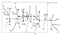
図1は、本発明の第1の実施例に係る逐次型光電変換装置の概略回路図である。逐次型光電変換装置とは、イメージセンサの各フォトダイオード出力の電荷リセットと光電荷蓄積をタイミングをずらしながら平行に行う光電変換装置を言う。 FIG. 1 is a schematic circuit diagram of a sequential photoelectric conversion apparatus according to the first embodiment of the present invention. The sequential photoelectric conversion device is a photoelectric conversion device that performs charge reset and photoelectric charge accumulation of each photodiode output of the image sensor in parallel while shifting the timing.
光電変換ブロックAnはnビット目の光電変換ブロックを示している。光電変換ブロックは、画素数分設けられており各光電変換ブロックのチャンネル選択スイッチ7を介して共通信号線11に接続されている。図7に光電変換装置の全体構成図を示す。
A photoelectric conversion block An indicates an nth bit photoelectric conversion block. The photoelectric conversion blocks are provided for the number of pixels, and are connected to the
本実施例の回路は、光電変換手段となるフォトダイオード1、リセット手段となるリセットスイッチ2、増幅手段3、電荷転送手段となる転送スイッチ4、容量5、MOSソースフォロアを形成するMOSトランジスタ6、チャンネル選択手段となるチャンネル選択スイッチ7、共通信号線11、第1の電流源8からなる。
The circuit of this embodiment includes a
増幅手段3はMOSソースフォロアやボルテージフォロアアンプ等で形成し、動作状態を選択するアンプイネーブル端子10を設けても良い。また、MOSトランジスタ6のゲートとソース間には寄生容量9が存在する。
The amplifying
図2は、本発明の第1の実施例に係る逐次型光電変換装置の概略回路図に対応したタイミングチャートである。 FIG. 2 is a timing chart corresponding to the schematic circuit diagram of the sequential photoelectric conversion apparatus according to the first embodiment of the present invention.
φR(n)によりリセットスイッチ2がオンすると、フォトダイオード1の出力端子Vdiは基準電圧Vresetに固定され、リセットスイッチ2がオフすると、Vdiの電圧はVresetにオフノイズが加算された値になる。このオフノイズは、リセットする度に電位がゆらぐので、ランダムノイズとなる。したがって、ランダムノイズを防ぐためには、リセットした後のアンプ3の出力電圧と、その後、フォトダイオードが光電荷を蓄積した後のアンプ3の出力電圧の差をとればよい。
When the
そこで図2のように、φR(n)によりリセットスイッチ2がオフした後、φT1(n)により転送スイッチ4をオンして、TRの期間で基準信号を容量5に読み出す。基準信号は、1周期の間、容量5に保持される。この間にフォトダイオード1には、光電荷が蓄積し、Vdiの電位は光電荷の量に応じて変動している。次の周期のφSCH(n)によりチャンネル選択スイッチ7をオンすると、REFの期間に、容量5に保持された基準信号が共通信号線11に読み出される。次に、φT1(n)をオンし、TSの期間でフォトダイオードに蓄積した電荷に応じた光信号を容量5に読み出すと、この光信号が共通信号線11に読み出される。φT1(n)をオンすると、容量5に光信号が蓄積されるが、φT1(n)をオンしている期間TSの間に、V1の電位がセットリングするように増幅手段3のドライバビリティーを設定すれば、φSCH(n)の期間を短くでき、高速の読み出しが可能である。
Therefore, as shown in FIG. 2, after the
以上の動作により、φSCH(n)のREFの期間とSIGの期間の共通信号線11の出力電圧VOUTの差を取れば、固定パターンノイズとリセットスイッチ2によるランダムノイズを除去できる。
With the above operation, the fixed pattern noise and the random noise due to the
そして、φT1(n)をオフしてから、φSCH(n)をオフし、φR(n)をオンして、次回のフォトダイオードのリセットを行い、再びφT1(n)をオンして、TRの期間で基準信号を容量5に読み出す。
Then, after turning off φT1 (n), turning off φSCH (n), turning on φR (n), resetting the next photodiode, turning on φT1 (n) again, and turning on TR The reference signal is read out to the
φSCH(n)がオフしてから、次のビットのチャンネル選択スイッチ7がφSCH(n+1)によってオンし、次のビットの基準信号の読み出しが始まる。n+1ビット目の他のパルスは、nビット目のパルスよりも、全てφSCHのオン期間だけ後ろにずれる。各受光素子の蓄積期間はφR(n)がオフしてから、次の周期のφT1(n)のTSの期間の終了までであるが、この期間もビットによってずれることになる。
After φSCH (n) is turned off, the channel select
読み出した基準信号と光信号は、相関2重サンプリング回路等により差をとる。これは、例えば、従来例の図16のブロックCの回路で可能である。 A difference between the read reference signal and the optical signal is obtained by a correlated double sampling circuit or the like. This is possible, for example, with the circuit of block C in FIG.
図3は、本発明の第2の実施例に係る逐次型光電変換装置の概略回路図である。図1との違いは、MOSトランジスタ6のソースに、第2の電流源51が接続されている点である。この第2の電流源はイネーブル信号φRRによってオン・オフし、オン状態では第1の電流源8と同程度の電流が流れるように設計されている。
FIG. 3 is a schematic circuit diagram of a sequential photoelectric conversion apparatus according to the second embodiment of the present invention. The difference from FIG. 1 is that the second
図5は、本発明の第2の実施例に係る逐次型光電変換装置の概略回路図に対応したタイミングチャートである。 FIG. 5 is a timing chart corresponding to the schematic circuit diagram of the sequential photoelectric conversion apparatus according to the second embodiment of the present invention.
φR(n)によりリセットスイッチ2がオンすると、フォトダイオード1の出力端子Vdiは基準電圧Vresetに固定され、リセットスイッチ2がオフすると、Vdiの電圧はVresetにオフノイズが加算された値になる。このオフノイズは、リセットする度に電位がゆらぐので、ランダムノイズとなる。したがって、ランダムノイズを防ぐためには、リセットした後のアンプ3の出力電圧と、その後、フォトダイオードが光電荷を蓄積した後のアンプ3の出力電圧の差をとればよい。
When the
そこで、図5のように、φR(n)によりリセットスイッチ2がオフした後、φT1(n)により転送スイッチ4をオンして、TRの期間で基準信号を容量5に読み出す。このとき、イネーブル信号φRR(n)により第2の電流源51をオン状態にする。基準信号は、1周期の間、容量5に保持される。この間にフォトダイオード1には、光電荷が蓄積し、Vdiの電位は光電荷の量に応じて変動している。次の周期のφSCH(n)によりチャンネル選択スイッチ7をオンすると、REFの期間に、容量5に保持された基準信号が共通信号線11に読み出される。次に、φT1(n)をオンし、光信号を容量5に読み出すと、この光信号が共通信号線11に読み出される。
Therefore, as shown in FIG. 5, after the
このとき、第1の電流源8はオン状態にし、第2の電流源51はオフ状態にする。第1の電流源8と第2の電流源51は同程度のオン電流が流れるように設計されているので、R1の期間で基準信号を容量23に読み出すときと、S1の期間で光信号を容量23に読み出すときのMOSトランジスタ6のソース電位を同程度にすることが出来る。従って、容量5に蓄える電荷への寄生容量9の影響を小さくすることが出来て、結果として暗出力電圧のオフセットを小さく出来る。
At this time, the first current source 8 is turned on, and the second
以上の動作により、φSCH(n)のREFの期間とSIGの期間の共通信号線11の出力電圧VOUTの差を取れば、固定パターンノイズとリセットスイッチ2によるランダムノイズを除去できる。次に、φT1(n)をオフしてから、φSCH(n)をオフし、φR(n)をオンして、次回のフォトダイオードのリセットを行い、再びφT1(n)をオンして、TRの期間で基準信号を容量5に読み出す。
With the above operation, the fixed pattern noise and the random noise due to the
φSCH(n)がオフしてから、次のビットのチャンネル選択スイッチ7がφSCH(n+1)によってオンし、次のビットの基準信号の読み出しが始まる。n+1ビット目の他のパルスは、nビット目のパルスよりも、全てφSCHのオン期間だけ後ろにずれる。
After φSCH (n) is turned off, the channel
基準信号と光信号は、相関2重サンプリング回路等により差をとる。これは、例えば、従来例の図16のブロックCの回路で可能である。 A difference between the reference signal and the optical signal is obtained by a correlated double sampling circuit or the like. This is possible, for example, with the circuit of block C in FIG.
図4は、本発明の第2の実施例に係る逐次型光電変換装置の回路図である。図3のリセットスイッチ2はMOSスイッチ35、増幅手段3はMOSソースフォロア30と電流源31、転送スイッチ4は、トランスミッションゲート32とダミースイッチ33、第2の電流源51はMOS電流源34、チャンネル選択スイッチ7はMOSスイッチ36、第1の電流源8はMOS電流源37で置き換えている。なお、MOS電流源34を取り除けば、第1の実施例に係る逐次型光電変換装置の回路図となる。
FIG. 4 is a circuit diagram of a sequential photoelectric conversion apparatus according to the second embodiment of the present invention. 3, the
図6は、本発明の第2の実施例に係る逐次型光電変換装置の回路図に対応したタイミングチャートである。図5との違いは、φSELがφI1に変わった点である。また、φT1Xは図6に示さないがφT1の反転である。 FIG. 6 is a timing chart corresponding to the circuit diagram of the sequential photoelectric conversion apparatus according to the second embodiment of the present invention. The difference from FIG. 5 is that φSEL is changed to φI1. Further, φT1X is an inversion of φT1 although not shown in FIG.
図4の回路では、アンプ30のオン・オフを電流源31のゲート電圧でコントロールする。すなわち、φI1が電源電圧のとき電流は流れずアンプ30はオフ状態であり、φI1が電源電圧よりも低い適当な電圧のとき電流が流れアンプ30はオン状態である。
In the circuit of FIG. 4, on / off of the
図2の回路ではMOSソースフォロア30の基板電位とソース電位を共通としているので、ゲインをほぼ1にできる。
In the circuit of FIG. 2, since the substrate potential and the source potential of the
また、基準信号REFを読み出すときはφT1のオフノイズが乗った状態のV1の電位を読み出すが、光信号SIGを読み出すときはφT1のオフノイズが乗っていない状態のV1の電位を読み出している。このため、φT1のオフノイズ分が、暗出力オフセットとなってしまう。これを小さくするために、転送スイッチをトランスミッションゲート32とし、ダミースイッチ33を設けている。トランスミッションゲートのNMOSとPMOSのトランジスタサイズは同じにし、ダミースイッチ33のNMOSとPMOSのトランジスタサイズは、トランスミッションゲートのトランジスタサイズのゲート面積の半分にする。
Further, when reading the reference signal REF, the potential of V1 in the state where the off-noise of φT1 is applied is read, but when reading the optical signal SIG, the potential of V1 in the state where no off-noise of φT1 is applied is read out. For this reason, the off-noise component of φT1 becomes a dark output offset. In order to reduce this, the transfer switch is a
φRRはGND電位のとき、MOS電流源34はオフ状態で、適当な電位のとき、MOS電流源34はオン状態となる。オン状態のφRRの電位は、MOS電流源34の電流がMOS電流源37の電流と同程度になるように設計する。簡単のために、MOS電流源34のサイズを適当に定め、オン状態のφRRの電位を電源電圧とすることもできる。以上は、MOSトランジスタ6とMOS電流源34とMOS電流源37が共にNMOSの場合であるが、共にPMOSであっても同様にできる。
When φRR is at the GND potential, the MOS
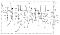
図8は、本発明の第3の実施例に係る一括型光電変換装置の概略回路図である。一括型光電変換装置とは、イメージセンサの各フォトダイオード出力の電荷リセットと光電荷蓄積を同時タイミングで平行に行う光電変換装置を言う。光電変換ブロックAnはnビット目の光電変換ブロックを示している。画素数分設けられた光電変換ブロックは、各光電変換ブロックのチャンネル選択スイッチ7を介して共通信号線11に接続されている。図7に光電変換装置の全体構成図を示す。
FIG. 8 is a schematic circuit diagram of a collective photoelectric conversion device according to the third embodiment of the present invention. The collective photoelectric conversion device refers to a photoelectric conversion device that performs charge reset and photoelectric charge accumulation of each photodiode output of the image sensor in parallel at the same timing. A photoelectric conversion block An indicates an nth bit photoelectric conversion block. The photoelectric conversion blocks provided for the number of pixels are connected to the
本実施例の回路は、光電変換手段となるフォトダイオード1、電荷転送手段となる転送スイッチ18、19、20、リセット手段となるリセットスイッチ2、増幅手段15、16、17、容量21、22、23、MOSソースフォロアを形成するMOSトランジスタ6、チャンネル選択手段となるチャンネル選択スイッチ7、共通信号線11、第1の電流源8からなる。増幅手段15、16、17はMOSソースフォロアやボルテージフォロアアンプ等で形成し、動作状態を選択するアンプイネーブル端子12、13、14を設けても良い。また、 MOSトランジスタ6のゲートとソース間には寄生容量9が存在する。
The circuit of this embodiment includes a
図10は、本発明の第3の実施例に係る一括型光電変換装置の概略回路図に対応したタイミングチャートである。φR、φT1、φSEL1は全ビットについて同時に動作する。φT2の光信号を転送する期間S1とφSEL2の光信号を転送する期間も全ビットについて同時に動作する。φT2の基準信号を転送する期間R1とφSEL2の基準信号を転送する期間とその他のパルスは、ビットによって動作するタイミングが異なるので、(n)付で表示している。 FIG. 10 is a timing chart corresponding to the schematic circuit diagram of the collective photoelectric conversion device according to the third embodiment of the present invention. φR, φT1, and φSEL1 operate simultaneously for all bits. The period S1 during which the φT2 optical signal is transferred and the period during which the φSEL2 optical signal is transferred operate simultaneously for all bits. The period R1 for transferring the reference signal for φT2, the period for transferring the reference signal for φSEL2, and the other pulses are indicated with (n) because the timing of operation differs depending on the bit.
まず、nビット目の光電変換ブロックで基準信号を転送する動作について説明する。 First, the operation of transferring the reference signal in the nth photoelectric conversion block will be described.
φRのパルスR1によりリセットスイッチ2がオンすると、フォトダイオード1の出力端子Vdiは基準電圧Vresetに固定され、リセットスイッチ2がオフするとVdiの電圧はVresetにオフノイズが加算された値になる。このオフノイズは、リセットする度に電位がゆらぐのでランダムノイズとなる。ランダムノイズの影響を除く為には、リセットした後の第1のアンプ15の出力電圧と、その後にフォトダイオードが光電荷を蓄積した時の第1のアンプ15の出力電圧の差をとればよい。
When the
そこで図10のように、リセットスイッチ2がオフした後に、φT1のパルスR1により第1の転送スイッチ18をオンして、基準信号を第1の容量21に読み出し保持する。この後フォトダイオード1には、光電荷が蓄積しVdiの電位は光電荷の量に応じて変動する。この光電荷が蓄積する期間は、φRのパルスR1の終了からφT1のパルスS1の終了までのTS1となり、全てのビットについて同じ期間になる。
Therefore, as shown in FIG. 10, after the
次に、φT2(n)のパルスR1により第2の転送スイッチ19をオンして、基準信号を第2の容量22に読み出し、φT3(n)のパルスR1により第3の転送スイッチ20をオンして、基準信号を第3の容量23に読み出す。基準信号は、1周期の間、容量23に保持される。
Next, the
次に、nビット目の光電変換ブロックで光信号を転送する動作について説明する。 Next, an operation for transferring an optical signal in the n-th photoelectric conversion block will be described.
蓄積期間TS1の最後で、φT1のパルスS1により第1の転送スイッチ18をオンして、フォトダイオードに蓄積した電荷に応じた光信号を第1の容量21に読み出す。次に、φT2(n)のパルスS1により第2の転送スイッチ19をオンして、光信号を第2の容量22に読み出す。これは全てのビットで同時に行われる。
At the end of the accumulation period TS1, the
次に、nビット目の光電変換ブロックから基準信号と光信号を読み出しする動作について説明する。 Next, an operation for reading the reference signal and the optical signal from the n-th photoelectric conversion block will be described.
TS2の蓄積期間中に、φSCH(n)のパルスによりチャンネル選択スイッチ7を開くと、第3の容量23に保持されていた基準信号が共通信号線11に読み出される。この期間はφSCH(n)のR1の部分である。この基準信号は、φRのパルスR1により発生した基準信号である。次に、φT3(n)をオンしS1の期間で光信号を容量23に読み出すと、この光信号が共通信号線11に読み出される。
When the
φT3(n)をオンすると光信号が容量23に読み出されるが、φT3(n)をオンしている期間S1の間に、V1の電位がセットリングするように増幅手段17のドライバビリティーを設定すれば、φSCH(n)の期間を短くでき、高速の読み出しが可能である。
When φT3 (n) is turned on, the optical signal is read out to the
以上の動作により、φSCH(n)のR1とS1の期間における共通信号線11の出力電圧VOUTの差を取れば、固定パターンノイズとリセットスイッチ2によるランダムノイズを除去することが可能である。これは、両方に同じリセットパルスφRのオフノイズがのっており、両方の電圧の出力経路が同じであるからである。
With the above operation, fixed pattern noise and random noise due to the
更に、φT3(n)をオフしてからφSCH(n)をオフし、φT2(n)のパルスR2により第2の転送スイッチ19をオンして、φRのパルスR2が終了した後の基準信号を第2の容量22に読み出し、φT3(n)のパルスR2により第3の転送スイッチ20をオンして、基準信号を第3の容量23に読み出す。
Further, after φT3 (n) is turned off, φSCH (n) is turned off, the
一方、φSCH(n)がオフしてから、次のビットのチャンネル選択スイッチ7がφSCH(n+1)によってオンし、次のビットの基準信号の読み出しが始まる。n+1ビット目のφT2の基準信号を読み出すパルスやφT3のパルスは、nビット目のパルスよりも全てφSCHのオン期間だけ後ろにずれる。
On the other hand, after φSCH (n) is turned off, the
読み出した基準信号と光信号は、相関2重サンプリング回路等により差をとる。これは、例えば従来例の図16のブロックCの回路で可能である。 A difference between the read reference signal and the optical signal is obtained by a correlated double sampling circuit or the like. This is possible, for example, with the circuit of block C in FIG.
図8及び図10の実施例では、TS2の期間でフォトダイオードが蓄積動作中に、前の蓄積期間TS1の期間で蓄積した光信号を読み出すことができる。したがって、RGBの3色のLEDを順に点灯して、カラー画像データを読み取ることができる。たとえば、TS1の期間に赤のLEDを点灯し赤の成分を読み取り、TS2の期間に緑のLEDを点灯し緑の成分を読み取り、TS2の次の期間に青のLEDを点灯し青の成分を読み取ることができる。この場合、TS2の期間内に赤の光信号を読み出すことになる。 8 and 10, the optical signal accumulated in the previous accumulation period TS1 can be read out while the photodiode is accumulating in the period TS2. Therefore, the color image data can be read by sequentially turning on LEDs of three colors RGB. For example, the red LED is lit and the red component is read during the period of TS1, the green LED is lit and the green component is read during the period of TS2, the blue LED is lit and the blue component is read during the next period of TS2. Can be read. In this case, a red light signal is read out within the period TS2.
図9は、本発明の第3の実施例に係る一括型光電変換装置の回路図である。図8のリセットスイッチ2はMOSスイッチ35、増幅手段15、16、17はMOSソースフォロア38、40、42と電流源39、41、43、転送スイッチ18、19は、MOSスイッチ44、45、転送スイッチ20はトランスミッションゲート32とダミースイッチ33、チャンネル選択スイッチ7はMOSスイッチ36、第1の電流源8はMOS電流源37で置き換えている。
FIG. 9 is a circuit diagram of a collective photoelectric conversion device according to the third embodiment of the present invention. The
図11は、本発明の第3の実施例に係る一括型光電変換装置の回路図に対応したタイミングチャートである。図10との違いは、φSEL1、φSEL2、φSEL3、がそれぞれφI1、φI2、φI3、に変わった点である。また、φT3Xは図11に示さないがφT3の反転である。 FIG. 11 is a timing chart corresponding to the circuit diagram of the collective photoelectric conversion device according to the third embodiment of the present invention. The difference from FIG. 10 is that φSEL1, φSEL2, and φSEL3 are changed to φI1, φI2, and φI3, respectively. Further, φT3X is an inversion of φT3 although not shown in FIG.
図9の回路では、アンプ38、40、42のオン・オフを、それぞれ電流源39、41、43のゲート電圧でコントロールする。MOSソースフォロア38と42の基板電位とソース電位を共通としているので、ゲインをほぼ1にできる。
In the circuit of FIG. 9, on / off of the
また、基準信号R1を読み出すときはφT3のオフノイズが乗った状態のV1の電位を読み出すが、光信号S1を読み出すときはφT3のオフノイズが乗っていない状態のV1の電位を読み出している。このため、φT3のオフノイズ分が、暗出力オフセットとなってしまう。これを小さくするために、転送スイッチをトランスミッションゲート32とし、ダミースイッチ33を設けている。トランスミッションゲートのNMOSとPMOSのトランジスタサイズは同じにし、ダミースイッチ33のNMOSとPMOSのトランジスタサイズは、トランスミッションゲートのトランジスタサイズのゲート面積の半分にする。
Further, when reading the reference signal R1, the potential of V1 with φT3 off-noise is read, but when reading the optical signal S1, the potential of V1 without φT3 off-noise is read. For this reason, the off-noise component of φT3 becomes a dark output offset. In order to reduce this, the transfer switch is a
消費電流の観点では、φT3のパルスS1を短くして高速読み出しする必要があるが、そのためには、増幅手段14や電流源43の電流を大きくする必要がある。図10や図11の駆動方法では、φT3のパルスS1はビットによってずれるので、消費電流を分散させることができる。このことは、図10のφSEL3や図11のφI3がビットごとにずれていることで示されている。一方、φT1とφT2は全ビットで同時にオンする必要があるが、オンの期間を長くすることで、増幅手段15、16や電流源39、41の電流を低く抑えることができる。すなわち、図10や図11に示されるφT1とφT2のオン期間を、φSCHやφT3のオン期間よりも長くすれば良い。図10や図11では、φT2のR2の期間がφSCHのオン期間と同じに示されているが、φT2のR2の期間をφSCHのオン期間よりも長くしてもさしつかえない。
From the viewpoint of current consumption, it is necessary to shorten the pulse S1 of φT3 and perform high-speed reading. To that end, it is necessary to increase the current of the amplifying means 14 and the
また、φT2、φT3、φSCH等のパルスは、ビットごとにずれるように作る必要があるが、シフトレジスタのパルスから作ることができる。 Further, pulses such as φT2, φT3, and φSCH need to be generated so as to be shifted for each bit, but can be generated from a pulse of a shift register.
図12は、本発明の第4の実施例に係る一括型光電変換装置の概略回路図である。光電変換ブロックAnはnビット目の光電変換ブロックを示している。画素数分設けられた光電変換ブロックは、各光電変換ブロックのチャンネル選択スイッチ7を介して共通信号線11に接続されている。図7に光電変換装置の全体構成図を示す。
FIG. 12 is a schematic circuit diagram of a collective photoelectric conversion device according to the fourth embodiment of the present invention. A photoelectric conversion block An indicates an nth bit photoelectric conversion block. The photoelectric conversion blocks provided for the number of pixels are connected to the
本実施例の回路は、光電変換手段となるフォトダイオード1、電荷転送手段となる転送スイッチ18、19、20、リセット手段となるリセットスイッチ2、増幅手段15、16、17、容量21、22、23、MOSソースフォロアを形成するMOSトランジスタ6、MOSトランジスタ6のソースに接続された第2の電流源、チャンネル選択手段となるチャンネル選択スイッチ7、共通信号線11、第1の電流源8からなる。増幅手段15、16、17はMOSソースフォロアやボルテージフォロアアンプ等で形成し、動作状態を選択するアンプイネーブル端子12、13、14を設けても良い。また、MOSトランジスタ6のゲートとソース間には寄生容量9が存在する。
The circuit of this embodiment includes a
第2の電流源はイネーブル信号φRRによってオン・オフし、オン状態では第1の電流源8と同程度の電流が流れるように設計されている。 The second current source is turned on / off by an enable signal φRR, and is designed so that the same current as the first current source 8 flows in the on state.
図14は、本発明の第4の実施例に係る一括型光電変換装置の概略回路図に対応したタイミングチャートである。φR、φT1、φSEL1は全ビットについて同時に動作する。φT2の光信号を転送する期間S1とφSEL2の光信号を転送する期間も全ビットについて同時に動作する。φT2の基準信号を転送する期間R1とφSEL2の基準信号を転送する期間とその他のパルスは、ビットによって動作するタイミングが異なるので、(n)付で表示している。 FIG. 14 is a timing chart corresponding to the schematic circuit diagram of the collective photoelectric conversion device according to the fourth embodiment of the present invention. φR, φT1, and φSEL1 operate simultaneously for all bits. The period S1 during which the φT2 optical signal is transferred and the period during which the φSEL2 optical signal is transferred operate simultaneously for all bits. The period R1 for transferring the reference signal for φT2, the period for transferring the reference signal for φSEL2, and the other pulses are indicated with (n) because the timing of operation differs depending on the bit.
まず、nビット目の光電変換ブロックで基準信号を転送する動作について説明する。 First, the operation of transferring the reference signal in the nth photoelectric conversion block will be described.
φRのパルスR1によりリセットスイッチ2がオンすると、フォトダイオード1の出力端子Vdiは基準電圧Vresetに固定され、リセットスイッチ2がオフするとVdiの電圧はVresetにオフノイズが加算された値になる。このオフノイズは、リセットする度に電位がゆらぐのでランダムノイズとなる。ランダムノイズの影響を除く為には、リセットした後の第1のアンプ15の出力電圧と、その後にフォトダイオードが光電荷を蓄積した時の第1のアンプ15の出力電圧の差をとればよい。
When the
そこで図14のように、リセットスイッチ2がオフした後に、φT1のパルスR1により第1の転送スイッチ18をオンして、基準信号を第1の容量21に読み出し保持する。この後フォトダイオード1には、光電荷が蓄積しVdiの電位は光電荷の量に応じて変動する。この光電荷が蓄積する期間は、φRのパルスR1の終了からφT1のパルスS1の終了までのTS1となり、全てのビットについて同じ期間になる。
Therefore, as shown in FIG. 14, after the
次に、φT2(n)のパルスR1により第2の転送スイッチ19をオンして、基準信号を第2の容量22に読み出す。次に、φT3(n)のパルスR1により第3の転送スイッチ20をオンして、基準信号を第3の容量23に読み出す。このとき、イネーブル信号φRR(n)により第2の電流源51をオン状態にする。基準信号は、1周期の間、容量23に保持される。
Next, the
次に、nビット目の光電変換ブロックで光信号を転送する動作について説明する。 Next, an operation for transferring an optical signal in the n-th photoelectric conversion block will be described.
蓄積期間TS1の最後で、φT1のパルスS1により第1の転送スイッチ18をオンして、フォトダイオードに蓄積した電荷に応じた光信号を第1の容量21に読み出す。次に、φT2(n)のパルスS1により第2の転送スイッチ19をオンして、光信号を第2の容量22に読み出す。これは全てのビットで同時に行われる。
At the end of the accumulation period TS1, the
次に、nビット目の光電変換ブロックから基準信号と光信号を読み出しする動作について説明する。 Next, an operation for reading the reference signal and the optical signal from the n-th photoelectric conversion block will be described.
TS2の蓄積期間中に、φSCH(n)のパルスによりチャンネル選択スイッチ7を開くと、第3の容量23に保持されていた基準信号が共通信号線11に読み出される。この期間はφSCH(n)のR1の部分である。この基準信号は、φRのパルスR1により発生した基準信号である。次に、φT3(n)をオンしS1の期間で光信号を容量23に読み出すと、この光信号が共通信号線11に読み出される。
When the
このとき、第1の電流源8はオン状態にし、第2の電流源51はオフ状態にする。第1の電流源8と第2の電流源51は同程度のオン電流が流れるように設計されているので、R1の期間で基準信号を容量23に読み出すときと、S1の期間で光信号を容量23に読み出すときのMOSトランジスタ6のソース電位を同程度にすることが出来る。従って、容量23に蓄える電荷への寄生容量9の影響を小さくすることが出来て、結果として暗出力電圧のオフセットを小さく出来る。
At this time, the first current source 8 is turned on, and the second
また、φT3(n)をオンすると、光信号が容量23に読み出されるが、φT3(n)をオンしている期間S1の間に、V1の電位がセットリングするように増幅手段17のドライバビリティーを設定すれば、φSCH(n)の期間を短くでき、高速の読み出しが可能である。
When φT3 (n) is turned on, the optical signal is read out to the
以上の動作により、φSCH(n)のR1の期間とS1の期間の共通信号線11の出力電圧VOUTの差を取れば、固定パターンノイズとリセットスイッチ2によるランダムノイズを除去できる。これは、両方に同じリセットパルスφRのオフノイズがのっており、両方の電圧の出力経路が同じであるからである。
With the above operation, the fixed pattern noise and the random noise due to the
次に、φT3(n)をオフしてから、φSCH(n)をオフし、φT2(n)のR2の位置のパルスにより第2の転送スイッチ19をオンして、リセットパルスφRのR2の期間終了後の基準信号を第2の容量22に読み出す。次に、φT3(n)のR2の位置のパルスにより第3の転送スイッチ20をオンして、基準信号を第3の容量23に読み出す。
Next, φT3 (n) is turned off, φSCH (n) is turned off, the
一方、φSCH(n)がオフしてから、次のビットのチャンネル選択スイッチ7がφSCH(n+1)によってオンし、次のビットの基準信号の読み出しが始まる。n+1ビット目のφT2の基準信号を読み出すパルス、φT3、φRRのパルスは、nビット目のパルスよりも、全てφSCHのオン期間だけ後ろにずれる。
On the other hand, after φSCH (n) is turned off, the
基準信号と光信号は、相関2重サンプリング回路等により差をとる。これは、例えば、従来例の図16のブロックCの回路で可能である。 A difference between the reference signal and the optical signal is obtained by a correlated double sampling circuit or the like. This is possible, for example, with the circuit of block C in FIG.
図12、図14の実施例では、TS2の期間でフォトダイオードが蓄積動作中に、前の蓄積期間TS1の期間で蓄積した光信号を読み出すことができる。したがって、RGBの3色のLEDを順に点灯して、カラー画像データを読み取ることができる。たとえば、TS1の期間に赤のLEDを点灯し赤の成分を読み取り、TS2の期間に緑のLEDを点灯し緑の成分を読み取り、TS2の次の期間に青のLEDを点灯し青の成分を読み取ることができる。この場合、TS2の期間内に赤の光信号を読み出すことになる。 In the embodiment of FIGS. 12 and 14, the optical signal accumulated in the previous accumulation period TS1 can be read out while the photodiode is accumulating in the period TS2. Therefore, the color image data can be read by sequentially turning on LEDs of three colors RGB. For example, the red LED is lit and the red component is read during the period of TS1, the green LED is lit and the green component is read during the period of TS2, the blue LED is lit and the blue component is read during the next period of TS2. Can be read. In this case, a red light signal is read out within the period TS2.
図13は、本発明の第4の実施例に係る一括型光電変換装置の回路図である。図12のリセットスイッチ2はMOSスイッチ35、増幅手段15、16、17はMOSソースフォロア38、40、42と電流源39、41、43、転送スイッチ18、19は、MOSスイッチ44、45、転送スイッチ20はトランスミッションゲート32とダミースイッチ33、第2の電流源51はMOS電流源34、チャンネル選択スイッチ7はMOSスイッチ36、第1の電流源8はMOS電流源37で置き換えている。
FIG. 13 is a circuit diagram of a collective photoelectric conversion device according to the fourth embodiment of the present invention. 12, the
図15は、本発明の第4の実施例に係る一括型光電変換装置の回路図に対応したタイミングチャートである。図14との違いは、φSEL1、φSEL2、φSEL3、がそれぞれφI1、φI2、φI3、に変わった点である。また、φT3Xは図15に示さないがφT3の反転である。 FIG. 15 is a timing chart corresponding to the circuit diagram of the collective photoelectric conversion device according to the fourth embodiment of the present invention. The difference from FIG. 14 is that φSEL1, φSEL2, and φSEL3 are changed to φI1, φI2, and φI3, respectively. Further, φT3X is not shown in FIG. 15, but is an inversion of φT3.
図13の回路では、アンプ38、40、42のオン・オフを、それぞれ電流源39、41、43のゲート電圧でコントロールする。MOSソースフォロア38と42の基板電位とソース電位を共通としているので、ゲインをほぼ1にできる。
In the circuit of FIG. 13, on / off of the
また、基準信号R1を読み出すときはφT3のオフノイズが乗った状態のV1の電位を読み出すが、光信号S1を読み出すときはφT3のオフノイズが乗っていない状態のV1の電位を読み出している。このため、φT3のオフノイズ分が、暗出力オフセットとなってしまう。これを小さくするために、転送スイッチをトランスミッションゲート32とし、ダミースイッチ33を設けている。トランスミッションゲートのNMOSとPMOSのトランジスタサイズは同じにし、ダミースイッチ33のNMOSとPMOSのトランジスタサイズは、トランスミッションゲートのトランジスタサイズのゲート面積の半分にする。
Further, when reading the reference signal R1, the potential of V1 with φT3 off-noise is read, but when reading the optical signal S1, the potential of V1 without φT3 off-noise is read. For this reason, the off-noise component of φT3 becomes a dark output offset. In order to reduce this, the transfer switch is a
φRRはGND電位のとき、MOS電流源34はオフ状態で、適当な電位のとき、MOS電流源34はオン状態となる。オン状態のφRRの電位は、MOS電流源34の電流がMOS電流源37の電流と同程度になるように設計する。簡単のために、MOS電流源34のサイズを適当に定め、オン状態のφRRの電位を電源電圧とすることもできる。以上は、MOSトランジスタ6とMOS電流源34とMOS電流源37が共にNMOSの場合であるが、共にPMOSであっても同様にできる。
When φRR is at the GND potential, the MOS
消費電流の観点では、φT3のパルスS1を短くして高速読み出しする必要があるが、そのためには、増幅手段14や電流源43の電流を大きくする必要がある。しかし、図14や図15の駆動方法では、φT3のパルスはビットによってずれるので、消費電流を分散させることができる。このことは、図14のφSEL3や図15のφI3がビットごとにずれていることで示されている。一方、φT1やφT2は全ビット同時にオンする必要があるが、オンの期間を長くすることで、増幅手段15、16または、電流源39、41の電流を低く抑えることができる。すなわち、図14や図15に示される、φT1とφT2のオン期間を、φSCHやφT3のオン期間よりも長くすれば良い。図14や図15では、φT2のR2の期間がφSCHのオン期間と同じに示されているが、φT2のR2の期間をφSCHのオン期間よりも長くしてもさしつかえない。
From the viewpoint of current consumption, it is necessary to shorten the pulse S1 of φT3 and perform high-speed reading. To that end, it is necessary to increase the current of the amplifying means 14 and the
また、φT2、φT3、φSCH、φRR等のパルスは、ビットごとにずれるように作る必要があるが、シフトレジスタのパルスから作ることができる。 Further, pulses such as φT2, φT3, φSCH, and φRR need to be generated so as to be shifted for each bit, but can be generated from a pulse of a shift register.
以上の説明で、本発明は上述した各実施例に限定されるものではなく、その要旨を逸脱しない範囲で種々変形して実施することができる。 In the above description, the present invention is not limited to the above-described embodiments, and various modifications can be made without departing from the scope of the invention.
上記の回路は1つの半導体基盤上に形成し、リニアイメージセンサICとすることが可能である。また、このリニアイメージセンサICを複数個直線状に実装して、密着型イメージセンサを供給することができる。 The above circuit can be formed on one semiconductor substrate to be a linear image sensor IC. Further, a plurality of linear image sensor ICs can be mounted in a straight line to provide a contact image sensor.
本発明は、ファクシミリやイメージスキャナ等の画像読み取り装置に適用するリニアイメージセンサICと、イメージセンサICを複数実装した密着型イメージセンサに利用することができる。また、エリアイメージセンサICに適用できる。 The present invention can be used for a linear image sensor IC applied to an image reading apparatus such as a facsimile or an image scanner, and a contact image sensor on which a plurality of image sensor ICs are mounted. Further, it can be applied to an area image sensor IC.
1 フォトダイオード
2 リセットスイッチ
3 アンプ
4 転送スイッチ
5 容量
6 MOSトランジスタ
7 チャンネル選択スイッチ
8 第1の電流源
9 寄生容量
10,12,13,14 アンプイネーブル端子
11 共通信号線
15 第1のアンプ
16 第2のアンプ
17 第3のアンプ
18 第1の転送スイッチ
19 第2の転送スイッチ
20 第3の転送スイッチ
21 第1の容量
22 第2の容量
23 第3の容量
30 MOSソースフォロア
31 電流源
32 トランスミッションゲート
33 ダミースイッチ
34 MOS電流源
35 MOSスイッチ
36 MOSスイッチ
37 MOS電流源
38、40、42 MOSソースフォロア
39、41、43 電流源
32 トランスミッションゲート
44、45 MOSスイッチ
51 第2の電流源
101 フォトダイオード
102 リセットスイッチ
103 ソースフォロアアンプ
104 定電流源
105 読み出しスイッチ
106 共通信号線
107 信号線リセットスイッチ
108 寄生容量
109 オペアンプ
110 抵抗
111 抵抗
112 チップセレクトスイッチ
113 容量
114 MOSトランジスタ
115 容量
116 出力端子
An nビット目の光電変換ブロック
Bm mチップ目のイメージセンサICブロック
C クランプ回路
D 反転増幅器
1
7 Channel selection switch 8 First
10, 12, 13, 14 Amplifier enable terminal 11 Common signal line 15
18 First transfer switch
19 Second transfer switch
20
39, 41, 43
102
Claims (3)
前記光電変換手段の出力に接続されたリセット手段と、
前記光電変換手段の出力に接続された増幅手段と、
前記増幅手段の出力に一方の端子が接続された電荷転送手段と、
前記電荷転送手段のもう一方の端子に接続された容量と、
前記電荷転送手段のもう一方の端子に入力が接続されたソースフォロワアンプと、
前記ソースフォロワアンプの出力に接続されたチャンネル選択手段と、
前記チャンネル選択手段の出力が接続された共通信号線と、
前記共通信号線に接続された第1の電流源と、
前記ソースフォロワアンプの出力に接続された第2の電流源と、
を有することを特徴とする光電変換装置。 Photoelectric conversion means for generating an optical signal in response to incident light;
Reset means connected to the output of the photoelectric conversion means;
Amplifying means connected to the output of the photoelectric conversion means;
Charge transfer means having one terminal connected to the output of the amplification means;
A capacitor connected to the other terminal of the charge transfer means;
A source follower amplifier having an input connected to the other terminal of the charge transfer means;
Channel selection means connected to the output of the source follower amplifier;
A common signal line to which the output of the channel selection means is connected;
A first current source connected to the common signal line;
A second current source connected to the output of the source follower amplifier;
A photoelectric conversion device comprising:
前記電荷転送手段がオンし、前記基準信号を前記容量に読み出しているときに、前記第2の電流源がオンする
ことを特徴とする請求項1記載の光電変換装置。 When the charge transfer means and the channel selection means are turned on and the optical signal is read out to the common signal line, the first current source is turned on,
2. The photoelectric conversion device according to claim 1, wherein the second current source is turned on when the charge transfer unit is turned on and the reference signal is read out to the capacitor.
第2の期間において、前記光電変換手段は入射した光に応じた光信号を発生し、
第3の期間において、前記チャンネル選択手段がオンして、前記容量から第1の期間に保持した基準信号を前記共通信号線に読み出し、
第4の期間において、前記電荷転送手段がオンして、前期第2の期間に前記光電変換手段に発生した光信号を前記共通信号線に読み出す、
ことを特徴とする請求項1または2記載の光電変換装置。 In the first period, the capacitor holds a reference signal generated by the reset unit resetting the photoelectric conversion unit,
In the second period, the photoelectric conversion means generates an optical signal corresponding to the incident light,
In the third period, the channel selection unit is turned on, and the reference signal held in the first period is read from the capacitor to the common signal line,
In the fourth period, the charge transfer unit is turned on, and the optical signal generated in the photoelectric conversion unit in the second period is read out to the common signal line.
The photoelectric conversion device according to claim 1, wherein
Priority Applications (4)
| Application Number | Priority Date | Filing Date | Title |
|---|---|---|---|
| JP2004019667A JP4146365B2 (en) | 2003-02-26 | 2004-01-28 | Photoelectric conversion device and driving method |
| US10/784,419 US7102115B2 (en) | 2003-02-26 | 2004-02-23 | Photoelectric converter and a method of driving the same |
| CNB2004100067883A CN100394758C (en) | 2003-02-26 | 2004-02-26 | Optoelectronic converter and drive method therefor |
| US11/501,630 US7394054B2 (en) | 2003-02-26 | 2006-08-09 | Photoelectric converter and a method of driving the same |
Applications Claiming Priority (3)
| Application Number | Priority Date | Filing Date | Title |
|---|---|---|---|
| JP2003048592 | 2003-02-26 | ||
| JP2003049572 | 2003-02-26 | ||
| JP2004019667A JP4146365B2 (en) | 2003-02-26 | 2004-01-28 | Photoelectric conversion device and driving method |
Publications (3)
| Publication Number | Publication Date |
|---|---|
| JP2004282716A JP2004282716A (en) | 2004-10-07 |
| JP2004282716A5 JP2004282716A5 (en) | 2007-02-15 |
| JP4146365B2 true JP4146365B2 (en) | 2008-09-10 |
Family
ID=33303675
Family Applications (1)
| Application Number | Title | Priority Date | Filing Date |
|---|---|---|---|
| JP2004019667A Expired - Fee Related JP4146365B2 (en) | 2003-02-26 | 2004-01-28 | Photoelectric conversion device and driving method |
Country Status (3)
| Country | Link |
|---|---|
| US (2) | US7102115B2 (en) |
| JP (1) | JP4146365B2 (en) |
| CN (1) | CN100394758C (en) |
Families Citing this family (16)
| Publication number | Priority date | Publication date | Assignee | Title |
|---|---|---|---|---|
| US9077022B2 (en) * | 2004-10-29 | 2015-07-07 | Medtronic, Inc. | Lithium-ion battery |
| JP4614286B2 (en) * | 2006-06-12 | 2011-01-19 | セイコーインスツル株式会社 | Photoelectric conversion device, image sensor, optical reader |
| JP5004327B2 (en) * | 2006-08-08 | 2012-08-22 | キヤノン株式会社 | Photoelectric conversion device and imaging system |
| JP2008219282A (en) * | 2007-03-01 | 2008-09-18 | Seiko Instruments Inc | Photoelectric conversion device |
| JP5305387B2 (en) * | 2007-12-25 | 2013-10-02 | セイコーインスツル株式会社 | Photodetection device and image display device |
| JP5296417B2 (en) | 2008-05-29 | 2013-09-25 | セイコーインスツル株式会社 | Photoelectric conversion device |
| JP5288965B2 (en) * | 2008-09-22 | 2013-09-11 | キヤノン株式会社 | Solid-state imaging device and driving method thereof |
| JP5257176B2 (en) * | 2009-03-18 | 2013-08-07 | ソニー株式会社 | Solid-state imaging device, driving method of solid-state imaging device, and electronic apparatus |
| US8754610B2 (en) * | 2009-05-22 | 2014-06-17 | Qualcomm Incorporated | System and method for supplying power to a load |
| JP2011176552A (en) * | 2010-02-24 | 2011-09-08 | Renesas Electronics Corp | Optical amplifier circuit and photocoupler |
| JP5482286B2 (en) * | 2010-02-25 | 2014-05-07 | ソニー株式会社 | Radiation imaging apparatus and driving method thereof |
| JP5713651B2 (en) * | 2010-12-10 | 2015-05-07 | キヤノン株式会社 | Photoelectric conversion device, camera system, and driving method of photoelectric conversion device |
| KR101982278B1 (en) * | 2012-03-26 | 2019-08-28 | 삼성전자주식회사 | Digital Silicon Photomultiplier Detector Cell |
| JP2015133617A (en) * | 2014-01-14 | 2015-07-23 | 株式会社東芝 | Amplifier circuit, a/d converter and communication apparatus |
| KR102422059B1 (en) * | 2014-07-18 | 2022-07-15 | 가부시키가이샤 한도오따이 에네루기 켄큐쇼 | Semiconductor device, imaging device, and electronic device |
| US11750944B2 (en) * | 2021-05-28 | 2023-09-05 | Varex Imaging Corporation | Pixel noise cancellation system |
Family Cites Families (2)
| Publication number | Priority date | Publication date | Assignee | Title |
|---|---|---|---|---|
| US6369853B1 (en) * | 1997-11-13 | 2002-04-09 | Foveon, Inc. | Intra-pixel frame storage element, array, and electronic shutter method suitable for electronic still camera applications |
| JP3933972B2 (en) * | 2001-04-19 | 2007-06-20 | セイコーインスツル株式会社 | Photoelectric conversion device |
-
2004
- 2004-01-28 JP JP2004019667A patent/JP4146365B2/en not_active Expired - Fee Related
- 2004-02-23 US US10/784,419 patent/US7102115B2/en not_active Expired - Lifetime
- 2004-02-26 CN CNB2004100067883A patent/CN100394758C/en not_active Expired - Fee Related
-
2006
- 2006-08-09 US US11/501,630 patent/US7394054B2/en not_active Expired - Fee Related
Also Published As
| Publication number | Publication date |
|---|---|
| US7102115B2 (en) | 2006-09-05 |
| US20050035273A1 (en) | 2005-02-17 |
| JP2004282716A (en) | 2004-10-07 |
| CN100394758C (en) | 2008-06-11 |
| US7394054B2 (en) | 2008-07-01 |
| CN1543186A (en) | 2004-11-03 |
| US20060266932A1 (en) | 2006-11-30 |
Similar Documents
| Publication | Publication Date | Title |
|---|---|---|
| US7394054B2 (en) | Photoelectric converter and a method of driving the same | |
| US7378639B2 (en) | Photoelectric conversion device and image sensor having a reset potential of a common signal line being common to the potential of a reference voltage terminal | |
| US9407847B2 (en) | Solid state imaging apparatus and imaging system with writing memory selecting unit and reading memory selecting unit for outputting signals in an order of spatial arrangement | |
| US7501609B2 (en) | Image sensor with linearly mounted image sensor IC's | |
| JP4937380B2 (en) | CMOS image sensor | |
| US20100020217A1 (en) | Solid-state imaging device and camera | |
| US5998779A (en) | Photoelectric conversion apparatus | |
| US7189953B2 (en) | Signal processing circuit, image sensor IC, and signal processing method | |
| US20060227228A1 (en) | Color image sensing device and pixel data reading method thereof | |
| CN106713789B (en) | Image sensor with a plurality of pixels | |
| JP3933972B2 (en) | Photoelectric conversion device | |
| JP2008072324A (en) | Image sensor, module and electronic equipment | |
| US20180027197A1 (en) | Unit pixel apparatus and operation method thereof | |
| JP2005093549A (en) | Photoelectric converter and image sensor ic | |
| CN115022560A (en) | Image sensing device | |
| US20050036049A1 (en) | Image sensor IC | |
| JP2002204336A (en) | Photoelectric conversion apparatus | |
| JP2000299764A (en) | Image sensor unit and image reader using the sensor unit | |
| JP2005039379A (en) | Image sensor ic | |
| JP2000078373A (en) | Optic/electric converting device, image sensor module using the same, image sensor unit and image reader | |
| JP2005142470A (en) | Photoelectric converter and image sensor ic | |
| JP3903047B2 (en) | Photoelectric conversion device and contact image sensor | |
| KR100412995B1 (en) | Image sensor having parallel analog bus lines and column drive circuit | |
| JP3895689B2 (en) | Image sensor |
Legal Events
| Date | Code | Title | Description |
|---|---|---|---|
| A521 | Request for written amendment filed |
Free format text: JAPANESE INTERMEDIATE CODE: A523 Effective date: 20061225 |
|
| A621 | Written request for application examination |
Free format text: JAPANESE INTERMEDIATE CODE: A621 Effective date: 20061225 |
|
| A977 | Report on retrieval |
Free format text: JAPANESE INTERMEDIATE CODE: A971007 Effective date: 20080123 |
|
| A131 | Notification of reasons for refusal |
Free format text: JAPANESE INTERMEDIATE CODE: A131 Effective date: 20080129 |
|
| A521 | Request for written amendment filed |
Free format text: JAPANESE INTERMEDIATE CODE: A523 Effective date: 20080326 |
|
| TRDD | Decision of grant or rejection written | ||
| A01 | Written decision to grant a patent or to grant a registration (utility model) |
Free format text: JAPANESE INTERMEDIATE CODE: A01 Effective date: 20080610 |
|
| A01 | Written decision to grant a patent or to grant a registration (utility model) |
Free format text: JAPANESE INTERMEDIATE CODE: A01 |
|
| A61 | First payment of annual fees (during grant procedure) |
Free format text: JAPANESE INTERMEDIATE CODE: A61 Effective date: 20080619 |
|
| R150 | Certificate of patent or registration of utility model |
Free format text: JAPANESE INTERMEDIATE CODE: R150 Ref document number: 4146365 Country of ref document: JP Free format text: JAPANESE INTERMEDIATE CODE: R150 |
|
| FPAY | Renewal fee payment (event date is renewal date of database) |
Free format text: PAYMENT UNTIL: 20110627 Year of fee payment: 3 |
|
| RD01 | Notification of change of attorney |
Free format text: JAPANESE INTERMEDIATE CODE: A7421 Effective date: 20091108 |
|
| FPAY | Renewal fee payment (event date is renewal date of database) |
Free format text: PAYMENT UNTIL: 20110627 Year of fee payment: 3 |
|
| RD03 | Notification of appointment of power of attorney |
Free format text: JAPANESE INTERMEDIATE CODE: R3D03 |
|
| FPAY | Renewal fee payment (event date is renewal date of database) |
Free format text: PAYMENT UNTIL: 20120627 Year of fee payment: 4 |
|
| FPAY | Renewal fee payment (event date is renewal date of database) |
Free format text: PAYMENT UNTIL: 20130627 Year of fee payment: 5 |
|
| FPAY | Renewal fee payment (event date is renewal date of database) |
Free format text: PAYMENT UNTIL: 20130627 Year of fee payment: 5 |
|
| S111 | Request for change of ownership or part of ownership |
Free format text: JAPANESE INTERMEDIATE CODE: R313113 |
|
| R350 | Written notification of registration of transfer |
Free format text: JAPANESE INTERMEDIATE CODE: R350 |
|
| R250 | Receipt of annual fees |
Free format text: JAPANESE INTERMEDIATE CODE: R250 |
|
| R250 | Receipt of annual fees |
Free format text: JAPANESE INTERMEDIATE CODE: R250 |
|
| S533 | Written request for registration of change of name |
Free format text: JAPANESE INTERMEDIATE CODE: R313533 |
|
| R350 | Written notification of registration of transfer |
Free format text: JAPANESE INTERMEDIATE CODE: R350 |
|
| R250 | Receipt of annual fees |
Free format text: JAPANESE INTERMEDIATE CODE: R250 |
|
| R250 | Receipt of annual fees |
Free format text: JAPANESE INTERMEDIATE CODE: R250 |
|
| LAPS | Cancellation because of no payment of annual fees |