JP2004538506A - Optical film having micro-replicated structure - Google Patents
Optical film having micro-replicated structure Download PDFInfo
- Publication number
- JP2004538506A JP2004538506A JP2003519655A JP2003519655A JP2004538506A JP 2004538506 A JP2004538506 A JP 2004538506A JP 2003519655 A JP2003519655 A JP 2003519655A JP 2003519655 A JP2003519655 A JP 2003519655A JP 2004538506 A JP2004538506 A JP 2004538506A
- Authority
- JP
- Japan
- Prior art keywords
- light
- light directing
- prism
- film
- axis
- Prior art date
- Legal status (The legal status is an assumption and is not a legal conclusion. Google has not performed a legal analysis and makes no representation as to the accuracy of the status listed.)
- Pending
Links
Images

Classifications
-
- G—PHYSICS
- G02—OPTICS
- G02B—OPTICAL ELEMENTS, SYSTEMS OR APPARATUS
- G02B5/00—Optical elements other than lenses
- G02B5/02—Diffusing elements; Afocal elements
- G02B5/0205—Diffusing elements; Afocal elements characterised by the diffusing properties
- G02B5/0236—Diffusing elements; Afocal elements characterised by the diffusing properties the diffusion taking place within the volume of the element
- G02B5/0242—Diffusing elements; Afocal elements characterised by the diffusing properties the diffusion taking place within the volume of the element by means of dispersed particles
-
- G—PHYSICS
- G02—OPTICS
- G02B—OPTICAL ELEMENTS, SYSTEMS OR APPARATUS
- G02B5/00—Optical elements other than lenses
-
- G—PHYSICS
- G02—OPTICS
- G02B—OPTICAL ELEMENTS, SYSTEMS OR APPARATUS
- G02B5/00—Optical elements other than lenses
- G02B5/02—Diffusing elements; Afocal elements
- G02B5/0205—Diffusing elements; Afocal elements characterised by the diffusing properties
- G02B5/021—Diffusing elements; Afocal elements characterised by the diffusing properties the diffusion taking place at the element's surface, e.g. by means of surface roughening or microprismatic structures
-
- G—PHYSICS
- G02—OPTICS
- G02B—OPTICAL ELEMENTS, SYSTEMS OR APPARATUS
- G02B5/00—Optical elements other than lenses
- G02B5/02—Diffusing elements; Afocal elements
- G02B5/0273—Diffusing elements; Afocal elements characterized by the use
- G02B5/0284—Diffusing elements; Afocal elements characterized by the use used in reflection
-
- G—PHYSICS
- G02—OPTICS
- G02B—OPTICAL ELEMENTS, SYSTEMS OR APPARATUS
- G02B5/00—Optical elements other than lenses
- G02B5/04—Prisms
- G02B5/045—Prism arrays
-
- G—PHYSICS
- G02—OPTICS
- G02B—OPTICAL ELEMENTS, SYSTEMS OR APPARATUS
- G02B5/00—Optical elements other than lenses
- G02B5/08—Mirrors
- G02B5/09—Multifaceted or polygonal mirrors, e.g. polygonal scanning mirrors; Fresnel mirrors
Abstract
反射型LCDなどの透明ディスプレイで用いるための光学フィルムに関する。光学フィルムは、入射光を反射する3次元のプリズム構造を有する。プリズム構造は、反射ファセットが所望の反射光パターンで反射光を指向するように構成される。さまざまな反射ファセットの形状および寸法によって、パターン形状および強度を制御することができる。一実施形態において、プリズム構造の高さは構造の2次元に沿って変化する。The present invention relates to an optical film for use in a transparent display such as a reflective LCD. The optical film has a three-dimensional prism structure that reflects incident light. The prism structure is configured such that the reflective facets direct the reflected light in a desired reflected light pattern. The shape and size of the various reflective facets can control the pattern shape and intensity. In one embodiment, the height of the prism structure varies along two dimensions of the structure.
Description
【技術分野】
【0001】
本発明は、光学フィルムおよびその作製方法に関する。さらに詳細には、本発明は、微細複製構造を有する層を含む光学フィルムに関する。
【背景技術】
【0002】
特殊な光変調器としても公知である反射型イメージング装置は、光の反射を局所的に変更することによって可視画像を形成する。このタイプの1つの有用な装置は、液晶ディスプレイすなわちLCDであり、画像を映すような態様で、偏光子の間に挟まれた液晶材料の電子的に処理される画素によって、ディスプレイに入射する光が透過されるか、反射されるかまたは遮断されるかのいずれかであり、それによってディスプレイの可視画像を形成する。
【0003】
LCDは、LCDの一主面(背面と呼ばれる)に入射する光によって照射されることが多く、他方の面、すなわち見ている人が存在する前面から出る。また、適切な反射体によって、前面、すなわち見ている側からLCDを照射し、反射体(一般に後方反射体と呼ばれる)によって反射される周辺光によって照射された画像を作成することも可能である。このような方法で照射されるLCDは、反射型LCDまたはRLCDと一般に呼ばれる。
【0004】
鏡面後方反射体および拡散後方反射体の両方が用いられており、それぞれある種の欠点を持っている。鏡面後方反射体は、金属的な画像外観を呈することができ、見ている人の背後または上部に位置している物体の画像を反射することができ、許容可能でないほど制限された視角を形成する可能性があり、特定の周辺光状態に応じてさまざまに変化する。さらに、鏡面反射体は、見ている人の頭部が最良の表示のために必要な入射照射光を遮断する恐れがあるように、入射光を反射する。他方、拡散反射体は、見ている人が存在する可能性のない位置に光を拡散する可能性がある点で、光の非効率的な使用という欠点があるため、より望ましい表示位置から照射光を外すことになる。これらの欠点は、米国特許第4,298,249号明細書にまとめられており、当該特許では、より適した位置からディスプレイを見ることができるような角度で入射光を反射するために、傾斜された反射面ストライプを有する後方反射体のほか、拡散面構造を備えている。同様に、米国特許第6,204,903号明細書は、特定の方向に反射光を指向するさまざまな構造的な形状を有する反射面および部分反射面を開示している。さまざまな光条件に適合するために、米国特許第5,128,787号明細書は、さまざまな光源からの光を所望の見ている位置に反射するためのさまざまな角度の構造を有する反射体を開示している。開示されている構造はまた、ディスプレイのさまざまな面および境界からの望ましくない鏡面反射光を受光する領域の外側の位置から画像を見ることができるため、グレアの影響を低減する利点も有する。
【発明の開示】
【発明が解決しようとする課題】
【0005】
本発明は、所定の角度で入射光を反射し、反射光の特定の方向への分散を生成する微細構造反射面を提供する。微細構造面は、その面に構築される小さな傾斜反射微細構造を有する一般的な全体形状を有する。傾斜微細構造は、所定の周期的な高さまたは高度によって規定される高さまたは高度において長手方向の変化を有する。高さは、一定の周期、可変であるが決定的な周期、不規則な周期またはそれらの組合せに応じて変化してもよい。
【課題を解決するための手段】
【0006】
本発明による微細構造面を作製するための適切なツールは、硬質銅などの適切な金属から構成される円筒ブランクに所望のパターンをダイヤモンドターニング加工し、フィルムのバッキング上に硬化可能な液体組成物の微細構造層にコーティングして形成するために、キャスティングツールとしてこの円筒を用いることによって製作されることができる。ダイヤモンドツールホルダに組み込まれた圧電素子によって、ダイヤモンドターニング処理に深さ関数を加えることができる。このタイプのツールホルダは、一般に高速ツールサーボまたはFTSと呼ばれている。また、一般に、高速サーボツールと呼ばれることもある。FTSを駆動するために用いられる信号は、単一周波数波または多重周波数波、雑音発生器からの信号および有用であると分かっている任意の他の信号を含んでいてもよい。たとえば、変動する高さの周波数範囲またはスペクトル波形を制限するために、信号をフィルタリングしてもよい。一般的に、深さ関数を生成するために用いることができる信号は、有用な微細構造を作製する際に特定の信号の適切さによってのみ制限される。本発明において用いるための信号を生成することが相対的に簡単であるために、所望の光学的効果を生成するさまざまな高さを形成するための適切な信号を求める場合に、きわめて経験的なアプローチを取ることも可能である。
【0007】
本願明細書で用いられるとき、「反射光学面」なる語は、ミラーなどのきわめて高い反射面および部分的にのみ反射し、光の相当量を透過する光学面の両方を含む。このタイプの部分反射体は、一般に半透過光学面と呼ばれる。本発明の反射面は、たとえば、銀などの適切な金属によって金属化することによって、反射を形成することができる。また、保護コーティングおよび他の面調整コーティングを組み込んでもよい。
【0008】
本発明の反射面を有する光学フィルムは、有効範囲の方向に光を反射するように設計することができ、利用可能な光をより効率的に利用し、グレア効果を避けることができるような光の厳密に制御された分布を形成することができるため、LCD用の後方反射体として有用である。
【0009】
反射光分布に対して拡散成分または他の指向性成分を形成するために、傾斜角および深さ関数によって規定される微細構造に加えて、ツールの化学エッチングなどのさらなる面処理も用いることができる。ツールの耐久性および微細構造物製品の表面の品質を改善する際に、ツールのメッキが有用である場合もある。
【0010】
特に一態様において、本発明は、x軸、y軸およびz軸を有する光指向フィルムであって、第1の構造面および対向する面を有するフィルムに関する。構造面は、その上に複数のプリズム構造を有し、プリズム構造は、略x軸に沿って延在し、隣接するプリズム構造の間にy軸に沿って間隙を有する。構造はまたz軸に沿って高さを有し、プリズム構造の高さは反復周期でx軸に沿って変動する。
【0011】
別の態様において、本発明は、微細複製光反射フィルムであって、長さを有する複数のプリズム構造を含み、複数のプリズム構造のそれぞれが反復周期において長さに沿って変動する高さを有するフィルムを含む光学素子に関する。金属フィルム層がフィルム上に存在していてもよい。
【0012】
また、本発明は、プログラム可能であるように制御された切削ツールを用いて作製され、x軸、y軸およびz軸を有する物品であって、略x軸に沿って延在する複数の構造を含み、複数の構造が隣接するプリズム構造の間でy軸に沿って間隙を有し、z軸に沿って高さを有し、構造の高さが反復パターンにおいてx軸に沿って変動する物品に関する。
【0013】
本発明によれば、反射構造付きフィルムを作製するための方法は、切削ツールを用いてブランクからマスターツールを機械加工するステップを含み、切削ツールはx方向、y方向およびz方向において移動可能である。機械加工ステップは、切削ツールとブランクを接触させるステップと、ブランクを切削するためにx方向において互いに関してブランクおよび切削ツールの少なくとも一方を移動するステップと、ブランクを切削するためにy方向において互いに関してブランクおよび切削ツールの少なくとも一方を移動するステップと、ブランクを切削するためにz方向において互いに関してブランクおよび切削ツールの少なくとも一方を移動するステップと、を含む。この機械加工用マスターツールにおいて、構造付きフィルムを作製し、次いで構造付きフィルムに反射コーティングを施す。
【0014】
本発明の方法は、化学エッチング、ビードブラストまたは他の確率的面調整技術などの方法を用いて作製されるフィルムより緻密、精確または精密である構造付きフィルムを提供する。化学エッチング、ビードブラストまたは他の確率的面調整技術などの方法は、1つのプリズム面から次のプリズム面までの精密な形をたとえば0.001マイクロメートルまで精密に再現することはできない。0.0001マイクロメートル未満はなおさらである。
【0015】
本発明は、添付図面と共に次の本発明のさまざまな実施形態の詳細な説明を考慮することによってより完全に理解されると思われる。
【発明を実施するための最良の形態】
【0016】
本発明は、反射型液晶ディスプレイ(RLCD)によって拡散反射される光のパターンを精密に形成することによって、RLCDにおける光の利用を改善する光学フィルムに関する。詳細に述べれば、特定の方向に反射するようにRLCDの後方反射体の面特徴物を設計することにより、より十分な均一性および明るさのために所望であるように反射光の分散が形成される。
【0017】
本願明細書で用いるとき、光学フィルムは、RLDCに対して所望の角度で光を反射する構造を含む構造面またはプリズム面を有するフィルムである。
【0018】
RLCDなどの反射型ディスプレイ装置10が、図1Aに示されている。ディスプレイ装置10は、追加光学素子14を通じて見ることができる表示情報を照射するために周辺光を用いる。追加光学素子14は、レンズ、タッチスクリーンまたはディスプレイ装置10の他の類似の素子であってもよい。素子14は、ディスプレイに特定の光学的性質を付与してもよく、ディスプレイの利用者からの入力を受理してもよい。ディスプレイ装置10は、上部偏光子22、液晶層24および下部偏光子26を含む光変調層20をさらに具備している。さらに、光指向フィルムを具備する光指向構成28が、下部偏光子26に隣接して配置される。光指向構成28に関する一部の実施形態では、下部偏光子26に接着することが有用かつ好都合であることが分かっている。液晶層を挟む2つの偏光子を有する素子に用いることがさらに一般的であるが、本発明の光指向フィルムはまた、唯一の偏光子を含むか、または偏光子を含まないディスプレイ素子(たとえば、ゲスト−ホストLCD)に組み込んでもよい。
【0019】
本願明細書では、さまざまな層を有する代表的なディスプレイ装置10について説明する。一般に、層のいずれかを変更または排除してもよく、依然として利用可能なディスプレイ10であることを理解されたい。また、追加層を追加することもできる。補償層またはフィルムは、ディスプレイ装置に具備することができる非等方性光学屈折フィルムである。利用可能なディスプレイと機能する異なる構造を形成するために、さまざまな層を再配置または再編成することができる。一部の実施形態において、単独層が、上述した2層として機能してもよい。さらに、より少数の個別層を形成するために、任意の複数の層を共に接着または積層してもよい。たとえば、偏光子または補償フィルムに光指向フィルムを積層することも可能である。本発明によって教示されるように、光指向フィルムを組み込んだディスプレイ装置10のあらゆる変形が、本願明細書に開示されている。
【0020】
再び図1Aを参照すると、周辺光源30は、入射する周辺光線32を生成する。このような図において、光源30からの光線32は、法線から角度aでディスプレイ装置に入射する。法線は、ディスプレイ面に垂直な方向である。入射光の一部は、ディスプレイ装置10の上面および内部の境界面によって、図1Aにはグレア光線34によって示されるグレアとして反射される。グレア光線34は、法線からグレア角bを有する。光線32と遭遇する境界面が境界反射面である場合には、グレア角bは入射角aに等しい。角度aは、存在しそうなさまざまな光源からの光を表す一定の範囲の値を含むことができるため、グレアは一定の範囲の視角にわたって見ることができるが、一般にたとえばグレア角bで1つ以上の明るさのピークを有する。
【0021】
入射光の大部分は光変調層20を通過し、光指向構成28によって反射され、それによって、ディスプレイ情報を照射し、画像光線38として出す。光指向構成28は、グレア角bとは実質的に異なる法線からの角度でディスプレイ10から出るように、画像光線38を指向するように設計される。これを一般に「ビームステアリング」と呼ぶ。量的には、画像光線38の特定の角度は、通常「屈折のスネルの法則」および光指向構成28の特定の特性によって支配される。
【0022】
図1Bを参照すると、図1Aに比べて拡大した図であり、構造層として示されている光指向構成28は、光変調層20によって生成される画像を所望の視角に向かって進めるように形成される。所望の視野角は、ディスプレイ10のグレア角度と実質的に異なる。光指向構成28はまた、ビームステアリングフィルムまたは傾斜ミラーフィルムとも呼ばれる場合がある。
【0023】
図1Bにおいて、入射光線32は、法線から角度aで線33によって表されるディスプレイ装置に入射する。法線は、ディスプレイ面に垂直な方向である。入射光線32は、ディスプレイ10のさまざまな構成部材によって屈折され、光線32に曲げを形成することによって、光線32’を形成する。グレアとして反射されない入射光のそのような部分は、光変調層20を通過し、光指向構成28によって反射されることによって、光変調層20を照射し、画像光線38を生成する。光指向構成28からの反射の一定の角度は、角度dによって表されるファセット36の角度に依存する。図1Bは単独の角度dを有する平坦な面としてファセット36を描いているが、特定の光条件および所望の視角に応じて、他の平坦でないファセットを用いることもでき、場合によってその方が好ましい場合もあることを十分に理解されたい。画像光線38がディスプレイ10を通過するとき、光線は屈折され、画像光線38に曲げを生じることから、法線から角度cで出ることを再び留意されたい。
【0024】
光指向構成28の特定の設計によって、画像を見ることができる視角の範囲およびピークの明るさが生じる視角の範囲を制御することができる。
【0025】
図1Aにおいて、画像光線38によって表されるように、ピーク画像角または最適な視角はディスプレイに対してほぼ直交している。その結果、位置44にいるディスプレイ装置10を見ている人は、画像光線38から角度bであるグレア画像に干渉されることなくくっきりとディスプレイ画像を見ることができる。さらに一般的に言えば、図1Bにおいて、ピーク画像角または最適視角は、画像光線38によって示されているように、ディスプレイ法線に対して角度cである。その結果、ディスプレイ装置10を見ている人は、ディスプレイに対して異なる角度bであるグレア画像に干渉されることなくくっきりとディスプレイ画像を見ることができる。
【0026】
図1Bにおいて分かるように、光指向構成28は、平滑面31および構造面33を有する構造を備えたプリズム状の光指向フィルムである。これについては、図面を参照して以下に詳細に述べる。平滑面31はディスプレイ10の後部とは別の側にあり、構造面は光変調層20に面し、光源30に面している。一部の実施形態において、構造面は、ディスプレイ10とは反対側に面するように位置することも可能である。面31はここでは平滑であるように記載されているが、面は粗面、波面、凹凸面であってもよく、またはその上にプリズム構造を有していてもよいことを理解されたい。本発明における光指向構成28およびその作用の変動については、以下にさらに詳細に述べる。
【0027】
本発明は、所望の範囲の角度にわたって所望の画像ビーム強度分散を形成するように光指向構成を設計することに関する。プリズム状の光指向フィルムの特定の構成によって、反射ビームの方向および角度範囲を変更することができる。RLCDの見ている人によって見られる光の分散を量的に表すために用いられる座標系が、図2Aに示されている。図2Aにおいて、点「P」は見ている人、輝度を測定するための光度計、光源または所定の他の品目であってもよい。点「P」は、方位角または単に方位と呼ぶ球座標θ、極角度と呼ぶφおよび半径座標と呼ぶρを有する。図2Aにおいて、見ている人によって見た場合に、点29はディスプレイ25上の点であり、縁23はディスプレイの上部である。反射光の分散の試験は、通常、極角度φが34°、方位角が0°で入射する平行光を用いて行われる。
【0028】
物理的な実例は、「ELDIM EZ コントラストモデル160R(ELDIM EZ Contrast model 160R)」光度計によって特徴付けられるとき、ビームステアリングの特定の効果を見ることができる。この光度計は、34°の入射平行光と共に反射モードで用いられる偏光光度計である。ELDIM光度計は、θおよびφの関数として反射輝度を測定し、0°(フィルムの法線)から80°(フィルム平面から10°)の範囲にある極角度にわたり、360°の全方位角範囲にわたってデータを座標で表す。光学ゲインは、同一条件下で測定されたホワイトランベルト標準の輝度に関して同一の輝度で正規化することによって得られる。図4、7、8、11、12、13、15および16において、この座標系を用いるグラフを見ることができる。θは円形グラフの周囲の度数として表され、グラフの一番上から始まって反時計方向に回転し、φはグラフの中心から半径方向の距離によって表される。
【0029】
図2Bは、プリズム構造を示す一般的な光指向構成の斜視図である。以下の実施例は、図2Bに示されている軸を用いて説明される。「x軸」または「x方向」は、構造の長手方向とも呼ばれ、隆起または微細構造の方向にある。「y軸」または「y方向」は、x軸に直交し、構造の面を横断するため、x軸およびy軸が基準平面29を規定し、光指向要素28の全体の形状を規定する。「z軸」または「z方向」は、x軸およびy軸によって形成される平面に垂直であり、光指向要素28の後方から前方に延在している。
【0030】
図2Cに描かれているタイプの円筒キャスティングツールを用いて、構造33を有する光指向構成を作製することができることが好都合である。図2Cにおいて、中心軸42を有する円筒ツール40は、円筒ブランクに環状の溝43を切削することによって作製される。適切な形成可能な材料が溝43と軟質ポリマーフィルムなどのバッキング材料との間に配置されるとき、溝は構造33を形成するために適した形状である。この種のツールについて述べる時、図2Cに示されているように、ツールに対するx方向およびy方向は、図2Bに示される光指向フィルム上のx方向およびy方向と一致している。
【0031】
本発明の光指向フィルムは、任意の形成可能な材料であってもよく、通常は透明である。アクリルおよびポリカーボネートをはじめとする紫外線重合可能な材料が、好ましい材料である。一般に、光指向フィルムを作製するための紫外線重合可能な組成物としては、たとえばメチルスチレンなどのアルキルスチレンモノマーなどのビニルモノマー、さまざまなコモノマーおよび/またはオリゴマーが挙げられる。一例では、組成物は、ビスフェノールA型エポキシジアクリレート、ノボラック型エポキシアクリレートのそれぞれおよびアルキルスチレン(たとえばメチルスチレン)をはじめとするビニルモノマーを含む。このような組成物は、「エポキシアクリレート」とみなされる。組成物の重合を開始してポリマー構造にするための遊離基源を与えるために、開始剤を追加してもよい。
【0032】
光指向フィルムにおいて用いるための好ましい紫外線重合可能なエポキシアクリレート組成物の一例は、一定の範囲の重量%によって列挙される以下の成分、すなわちビスフェノールAエポキシジアクリレート(55〜80%)、アクリル化エポキシ(1〜10%)、メチルスチレン(5〜25%)、光重合開始剤(0.25〜5%)(「ルシリンTPO」(Lucirin TPO)など)およびフッ素系界面活性剤(0.1〜0.3%)を含む。さらに、組成物は、約5%までの重量%の「イルガキュア184」(Irgacure 184)などの第2の光重合開始剤を含むことができる。これらの好ましい紫外線重合可能な組成物に関するさらなる詳細は、1999年10月22日に出願された米国特許出願第09/425,270号明細書(フォン(Fong))に記載されている。この特許明細書は、参照によって本願明細書に引用されるものとする。
【0033】
構造付きフィルムに反射コーティングを施すことができる。この反射コーティングは不透明であってもよく、銀、クロム、ニッケル、アルミニウム、チタン、アルミニウム−チタン合金、金、ジルコニウム、白金、パラジウム、アルミニウム−クロム合金、ロジウムまたはその組み合わせなどの金属であってもよい。好ましい反射金属コーティングは、銀である。反射コーティングは、連続であっても不連続であってもよい。不連続コーティングは、不連続コーティングを塗布することによって実現されてもよく、または連続コーティングの一部を除去することによって実現されてもよい。
【0034】
また、反射金属コーティングの性能および耐久性を改善するために、接着促進層、拡散障壁層および耐食層などの追加層を用いてもよい。好ましい耐食層の一例は、PCT公開特許出願WO01/31393明細書(ガードナー(Gardner)ら)に教示されている。この特許明細書は、参照によって本願明細書に引用されるものとする。
【0035】
拡散体層は、フィルムの欠陥を隠しモアレ効果を排除するために、構造付きフィルムの上に塗布されることが好ましい。本発明の光指向フィルムは、プリズム構造のために十分な光拡散を行うため、拡散体層は反射光の拡散を行う必要はない。拡散体層の一例は、ポリマービードまたはガラスビードを添加したポリメチル−メタクリレートポリマーである。
【0036】
ポリマーホストまたはキャリアは一般に、1.4〜1.5の屈折率を有するが、それより大きくても小さくてもよい。ビードは、ポリマーまたはガラスのいずれであっても、一般に1.35〜1.7の屈折率を有する。ビードとホストまたはキャリアのポリマーとの間の屈折率の差は、ビードおよびポリマー選択時の確定的特性である。屈折率の差は、大部分の用途では、0.01〜0.2であることが好ましく、0.02〜0.1であれば好ましい。
【0037】
ビードの平均直径は一般に、0.5〜20マイクロメートルであり、ハンドヘルド型ディスプレイ装置に用いる場合には、好ましいビード直径は2〜5マイクロメートルである。ポリマーに添加されたビードの量は、ビードの平均直径に左右される。小さな直径のビードはより小さなビード体積を添加することになり、より大きな直径のビードは大きな体積を添加することになる。一例として、屈折率の差が約0.05であり、ビード直径が約5マイクロメートルである場合には、有用な添加量は1%〜10%である。
【0038】
ビードを相当密に添加する場合には、拡散体層は、源の認識可能な画像がない状態で均一に明るい後方反射を形成するために、遠くの源からの光を分散し、欠陥およびアーティファクトを隠す。PCT公開特許出願WO97/01610明細書(ゲーツ(Goetz)ら)(この特許明細書は、参照によって本願明細書に引用されるものとする)は、欠陥および他のアーティファクトを隠すために、本発明のフィルムと共に用いることができる光拡散接着剤について教示している。
【0039】
不規則な散乱を生じるための別の技術としては、ツールの艶消し仕上げを施すことが挙げられる。溝を機械加工した後、構造のある銅のツールに酸エッチング、イオンめっきまたはビードブラストを施すことによって、艶消し仕上げを実現することができる。
【0040】
ディスプレイの色を変更するために、光指向構成の中の組成物または他の層に吸収染料または顔料を追加することができる。たとえば、周辺光で見る場合には、銀金属フィルムはわずかに黄色い外観を有することが多い。黄色の外観を補償し、無彩色の反射体を形成するために、構成に吸収染料を追加することができる。
【0041】
基板とツールとの間またはプリズムの逆形状を有する複数のキャビティを有する型に重合可能な組成物を塗布し、紫外線の下で組成物を重合してから、ツールからシートを分離するなどの当業界において公知のさまざまな異なる方法によって、光指向フィルムを作製することができる。プリズム構造を形成するための他の方法も公知であり、本発明において用いてもよい。プリズムのサイズが小さいことから、3次元構造を作製するための工程は、「微細複製」と呼ばれることが多い。3次元構造の微細複製のさらなる情報に関しては、たとえば、米国特許第5,183,597号(リュ−(Lu))を参照されたい。この特許明細書は、参照によって本願明細書に引用されるものとする。
【0042】
プリズムを形成するツールは、たとえば、同一出願による公開PCT特許WO00/48037明細書(この特許明細書は、参照によって本願明細書に引用されるものとする)に開示されているような機知のダイヤモンドターニング技術によって作製されてもよい。一般に、マスターツールは、ロールとして公知である円筒ブランクにダイヤモンドターニングを施すことによって作製される。ロールの面は通常、硬質銅からなるが、他の材料を用いてもよい。プリズム構造は、ロールの周囲の連続パターンで形成される。好ましい実施形態において、溝は、ねじ切りとして公知の技術によって形成される。ねじ切りでは、ダイヤモンドビットがターニングロールに並進する方向(y方向)に移動される間に、単独の連続する溝が(x方向において)ロール上に切削される。隣接する切込みの間の距離は、「ピッチ」と呼ぶ。一定のピッチを有する構造を形成するために、ダイヤモンドビットは一定の速度で移動される。
【0043】
一般的なダイヤモンドターニング技術は一般に、当業界では公知である。たとえば、PCT公開特許出願WO00/48037明細書を参照されたい。詳細は図7および図9とその説明を参照されたい。この公開特許は、ロールまたはドラムからマスターツールを作製するために用いることができるさまざまな装置および方法について述べている。このすべての開示内容は、参照によって本願明細書に引用されるものとする。
【0044】
本発明の光指向フィルムを作製するための方法に用いられる装置としては、高速サーボツールが挙げられる。WO00/48037明細書に開示されているように、高速ツールサーボ(FTS)は、切削ツールの位置を迅速に調整するソリッドステート圧電素子である。FTSの1つのタイプは、PZTとして公知である。FTSは、y方向およびz方向における切削ツールの移動の主軸を考慮し、y方向およびz方向における振動または他の微小な調節も行う。円筒が切削されるこの場合には、x方向における移動は、加工品の回転によって提供される。もし存在するのであれば、振動は一般に主切削ツールの移動に重ね合わせられる。さらに、または別法では、さらに別の特徴を提供するために、機械加工中、切削ツールを遥動またはx軸を中心にして回転してもよい。
【0045】
別の実施形態において、たとえば、一連のファセットを形成するために、周期的な傾斜関数によって形成される信号を用いてFTSを駆動することによって、隆起を形成するために、ダイヤモンド切削ツールのz方向移動を用いることができる。FTSの周波数応答の限界のために、1つの隆起の上部と次の隆起の下部との間の移行は、ある程度湾曲していてもよい。この種の傾斜関数は、本発明によれば、反射光の方向における正味の変化を形成する隆起状構造を形成することになる。切削がこのような態様で行われるとき、プリズム構造の長手方向は、切削されるツールの回転軸に垂直ではなく、平行である。さらに、円筒の1回転から次の回転まで同期を取る必要はないため、隆起は連続的であってもよく、またはツール全体にわたって同期していてもよく、より正確に言えば、隆起は非同期であってもよい。その結果、見ている人によって見られるときに、ディスプレイの照射の外観が改善されてもよい。キャスティングツールの湾曲した移行領域はまた、RLCDの外観を改善するように作用してもよい。さらなる光指向特徴部を形成するために、ダイヤモンド切削ツールは、反射光分散をさらに改良するために、曲線または他の適切な切削外形を備えていてもよい。
【0046】
上述以外の方法によって、プリズム構造を形成してもよい。たとえば、作製ツールを作製するために、マスターツールから注型硬化工程によって、マスターツールの構造をポリマー材料のベルトまたはウェブなどの他の媒体上に移動してもよい。次いで、プリズム構造を作製するためにこの作製ツールが用いられる。マスターツールを複製するために、電鋳法などの他の方法を用いてもよい。光指向フィルムを作製するための別の代替方法は、プリズム構造を形成するために、透明材料を直接切削または機械加工することである。
【0047】
本発明のプリズム構造および方法は、生成することができる信号、電子機器の周波数応答、FTSアクチュエータおよびツール面の機械特性によってのみ制限される。
【0048】
化学エッチング、ビードブラストまたは他の確率的面調整技術は通常、本発明の方法を用いて切削ツールによって実現される光拡散特性を得るために望ましい鋭い精密なプリズム構造および特徴部の幅を形成することはできない。このような許容可能ではない方法は、化学エッチング、ビードブラストまたは他の確率的面調整技術に関連する固有の不正確さおよび非反復性のために、本発明のようなきわめて精確な反復構造を形成することはできない。
【0049】
本発明は、以下の実施例でさらに説明および図示がなされる。実施例は本発明の例示であり、その詳細に範囲を限定するものと解釈すべきではない。実施例および本願明細書の残り部分を通して、「マイクロメートル」「ミクロン」なる語および「μm」は互換可能に用いられることを理解されたい。
【実施例】
【0050】
実施例の光指向フィルムは、ファセット外形を形成するためにダイヤモンドカッタまたはビットによって切削されたツールに紫外線感知エポキシアクリレート樹脂を微細複製することによって作製された。エポキシアクリレート樹脂はツール上にあり、5ミル(127マイクロメートル)のPET基板が樹脂の露出面に接着された。エポキシアクリレート樹脂が紫外線によって重合化された後、結果として生じる光指向フィルムがツールから除去された。
【0051】
実施例のそれぞれに関するマスターツールは、ダイヤモンドチップ切削ツールによって円筒に形成された銅シートまたはブランクを機械加工することによって作製された。機械加工工程を開始するために、z方向において銅ブランクに切削ツールを降ろした。円筒は、その中心軸を中心にして回転され、x方向に切削ツールを移動させた。y方向の円筒の面に沿って切削ツールを移動するために、円筒面に螺旋状の溝が形成される。一部の実施例の場合には、FTS(「高速ツールサーボ」または「高速サーボツール」)によってダイヤモンド切削ツールをz方向に移動した。機械加工された銅シートは、円筒から除去され、光指向フィルムを作製するために用いられた。
【0052】
実施例1−比較例
図3は、従来の光指向フィルム110を含む光指向構成100の第1の実施例の拡大断面図である。このようなフィルムの例としては、商品名「チルティッドミラーフィルム6.3」(Tilted Mirror Film 6.3)でミネソタ・マイニング・アンド・マニュファクチャリング・カンパニー(Minnesota Mining and Manufacturing Company)(3M)から入手可能である。y軸が図面の左から右に構造にわたって延び、z軸が図面の上から下に延びている状態で、光指向フィルム110のこの図は、図1Bに示された配向に類似している。x軸はページ中に延びている。
【0053】
光指向フィルム110は、平滑面112および構造面114を有する。構造面114は複数の三角プリズム140を含み、それぞれのプリズムは第1のプリズム面142および第2のプリズム面144を有し、谷143および山145を交互に繰り返す。第1のプリズム面142および第2のプリズム面144は、光指向フィルム110のピッチまたは周期を共に規定する。
【0054】
この実施形態において、光指向フィルム110は、角プリズム140の反復配列によって規定される。谷143から谷143まで、または山145から山145までを測定する反復するプリズム140のピッチは一般に、10μm〜100μmであり、約30μm〜80μmであればさらに好ましい。この実施例では、光指向フィルム110は、50マイクロメートルのピッチを有する。すなわち、反復する山145の間のy方向における長さは、50マイクロメートルである。
【0055】
光指向構成100によって反射される光の大部分が第1のプリズム面142によって反射されるため、第1のプリズム面142は一般に、「ファセット」または「反射ファセット」と呼ばれる。この実施例では、第1のプリズム面142は、y方向から6°の高さを有する。これはミラー角度とも呼ばれる。6°以外の角度を用いることができることを理解されたい。一般に、0〜30°の角度が用いられ、5〜9°であれば好ましい。
【0056】
各プリズム140は、第1のプリズム面142および第2のプリズム面144によって規定されるピーク角または内抱角を有する。各山45は、約86°の同一のピーク角を有する。
【0057】
光指向フィルム110は、上述の技術によって作製され、基板120上に配置される。さらに詳細に言えば、光指向フィルム110の平滑面112が、基板120に対して配置される。基板120上に光指向フィルム110を固定するために、接着剤を用いてもよい。またはプリズム140を形成する同一材料によって、基板120上に光指向フィルム110を接着してもよい。一部の実施形態において、基板120は、微細複製工程中に用いられる基板である。
【0058】
上に重なっているプリズム140は、反射金属コーティング130であり、光指向フィルム110の構造面114の上に配置されている。反射金属コーティングは、銀または任意の他の有用なコーティングであってもよい。
【0059】
上に重なっている金属コーティング層130は、ポリマービードまたはガラスビードを添加したポリメチル−メタクリレートポリマーなどの拡散体層135である。拡散体層135によって生じる拡散は、光指向フィルム110によって反射される光のピークを中心にして回転対称であるため、YZ平面における拡散の幅は、XZ平面における幅と同一である。
【0060】
比較例1の場合の具体的なプリズムおよびファセットの寸法は、以下の表1および表2に与えられる。すべての測定値は、マイクロメートル単位で与えられる。比較例1の光の反射率は、34°の入射平行光による反射モードにおいて用いられるELDIM EZ コントラストモデル160R(ELDIM EZ Contrast model 160R)で測定された。図4が結果グラフである。図4は、34°で鋭いグレアピークを示し、14°を中心にしてより広い後方反射されたピークを示している。全体的に見れば、反射光は中心により高い強度を有し、反射光が測定されなくなるまで徐々に減少する急勾配のピークとして示されている。
【0061】
本発明の光指向構成は、光指向フィルムを含み、所望の光分散を得るために、光の反射がプリズムによって操作されて導かれる点で比較例1のサンプルと異なる。大部分の場合には、先のとがった分散または鐘状の曲線の分散ではなく、光強度の平坦な分散またはトップハット状の分散が望ましい。光の平行ビームがプリズム特徴部によっても決定される方向において中心とする特定の角度の幅の中で一定の輝度で面によって散乱されるときに実現される。ビームステアリング特性は、0〜45°などの任意の適当な量だけグレア方向からずれた反射角度に偏っていてもよい。
【0062】
YZ平面における拡散
所望のプリズム面を形成するために、さまざまな技術を用いることができる。たとえば、各構造のファセット角度が隣接する構造と同一とならないように、構造を形成することができる。連続的または列ごとにファセット角度を変更することによって、光指向フィルムによる光の反射率が変更され、広範な角度にわたってYZ平面における拡散反射を形成する。
【0063】
実施例2−可変ファセットまたはプリズム角度
図5は、本発明の一態様による光指向フィルム210を含む光指向構成200の断面図である。y軸が図面の左から右に構造にわたって延び、z軸が図面の上から下に延びている状態で、光指向フィルム210のこの図は、図2に示されている配向と類似である。x軸はページ中に延びている。
【0064】
光指向フィルム210は、平滑面212および構造面214を有する。構造面214は、谷243および山245を規定する第1のプリズム面242および第2のプリズム面244を有する複数のプリズム240を形成する。第1のプリズム面242および第2のプリズム面244は、合成物を規定する1組の面を形成する。一般に、第1のプリズム面242は光を反射するために用いられ、第2のプリズム面244は光の反射または方向に関与しない。フィルム210の平滑面212は、基板220に隣接している。上に重なっている光方向フィルム210は、金属コーティング230および拡散体層235である。
【0065】
図3の光指向フィルム110のプリズム140と異なり、プリズム240は、すべて同一ではない。プリズム251、252、253、254を参照されたい。プリズム251はプリズム252と異なり、プリズム252はプリズム253と異なる。以下同様。光指向フィルム210のすべてのプリズムが光指向フィルム210の他のすべてのプリズムと異なっているというわけではないことを理解すべきである。正確に言えば、プリズムは隣接するプリズムと異なっていることが望ましい。図5を参照すると、プリズム252は隣接するプリズム251とは異なり、隣接するプリズム253とも異なる。2つの類似のプリズムの間に少なくとも2つのプリズムがあることが好ましく、2つの類似のプリズムの間に少なくとも4つのプリズムがあればさらに好ましい。目で見ることができるパターンの隠し場所を最適化するためには、特定のパターンまたは順序におけるプリズムのグループをクラスタ化することが有利である場合がある。
【0066】
プリズムは、反射ファセット、すなわち第1のプリズム面242が異なる傾斜を有する点で少なくとも異なり、それによって光拡散を増大させる。第1のプリズム面242の傾斜は一般に、平滑面212から測定される。さまざまなプリズムの第1のプリズム面242は一般に、第1のプリズム面242の傾斜に対して長さを変化させる。大部分の場合には、プリズムの山245は平滑面212から等距離であるが、一部の場合には、図5に示されているように、隣接する山245の高さは異なっていてもよい。
【0067】
拡散体層235は、ポリマービードまたはガラスビード236を添加したポリメチル−メタクリレートポリマーなどの低密度拡散体である。拡散体層235は、光指向構成100の拡散体層135より少ないビードを有し、欠陥およびアーティファクトを隠し、変化するプリズム角度によって生成される複数の反射ピークを組み込んでいる。
【0068】
より多くの光学的拡散を有する面を形成するために、高周波数周期または不規則な移動によって、マスターツールを作製するために用いられるダイヤモンド切削ビットを遥動することによって、YZ平面においてさまざまな角度を形成することができる。可変プリズム角度は、YZ平面において拡散を形成する。そのような拡散は、体積拡散体層235からの拡散に重ねられ、XZ平面およびYZ平面における拡散の幅を識別するために、さらなる自由度を与える。
【0069】
別の実施形態において、成形ダイヤモンド切削ビットによってマスターツールを切削することができ、平坦でないか、または直線でないビット形状を生じる。別法または追加として、前回の通過の場合とは異なる角度および異なる位置に配置された切削ビットを用いて、複数回通過することによってツールを切削することができる。結果として生じる平坦でないファセットは、YZ平面において、ビームステアリング効果および制御された光拡散を形成し、拡散体層の不規則な拡散に加える。ダイヤモンドビットまたはカッターの湾曲した切削エッジまたは直線でない切削エッジは、光の拡散を行うのに望ましい可変勾配を形成する。さらに、切削エッジの精確な形状は、拡散分布を決定する。
【0070】
実施例3Aおよび実施例3B―湾曲したファセット、非直線のファセット
図6は、本発明の別の態様による光指向構成300の断面図である。y軸が図面の左から右に構造にわたって延び、z軸が図面の上から下に延びている状態で、光指向構成300および光指向フィルム310のこの図は、図2に示されている配向と類似である。x軸はページ中に延びている。
【0071】
光指向構成300は、平滑面312および構造面314を有する光指向フィルム310を含む。光指向フィルム310は、谷343および山345を規定する第1のプリズム面342および第2のプリズム面344を有する複数のプリズム340を含む。平滑面312は、基板320に隣接している。上に重なっている光方向フィルム310は、金属コーティング330と、アーティファクトおよび欠陥を被覆するための低集積度のガラスビードまたはポリマービード336を有する拡散体層335と、である。
【0072】
第1のプリズム面342は、図3の面142および図5の面242などのような線形面ではなく、面に関連する曲率を有する。曲面は、平均面角度を中心にして2、3度から数度まで面の角度が広がる。すなわち、第1のプリズム面342に対する接線を引いた線は、平滑面312に対して0〜30°の角度であり、通常は4〜8°である。湾曲した第1のプリズム面342は、反射光に重みをかけて成形ローブとするために用いることができる反射ファセットを形成する。あるいは、湾曲した第1のプリズム面342は、正方形の反射分布を形成するように構成されてもよい。
【0073】
実施例3Aは光指向フィルム310のみであり、実施例3Bは光指向フィルム310上にコーティングが施され、拡散体層335は6%の体積集積度のポリマービードを有する。実施例3Aおよび3Bの場合の具体的なプリズムおよびファセットの寸法は、以下の表1および表2に与えられる。
【0074】
実施例3Aおよび3Bは、34°の入射平行光源による反射モードにおいて用いられるELDIM EZ コントラストモデル160R(ELDIM EZ Contrast model 160R)で特徴つけられ、その結果のグラフはそれぞれ、図7および図8に示されている。
【0075】
上記の実施例2と類似している実施例3Aの場合には、非直線のファセットが、図7に示されているように、YZ平面に拡散を形成する。図8において分かるように、そのような拡散は、体積拡散体層335からの拡散に重ねられ、XZ平面およびYZ平面における拡散の幅を識別するために、さらなる自由度を与える。
【0076】
実施例4−直線または曲面のセグメントを有するセグメント化された面
図9は、本発明の別の態様による光指向構成400の断面図である。光指向構成400は、平滑面412および構造面414を有する光指向フィルム410を含む。y軸が図面の左から右に構造にわたって延び、z軸が図面の上から下に延びている状態で、光指向フィルム410は、図2に示されている配向と類似の配向である。x軸はページ中に延びている。
【0077】
光指向フィルム410は、谷443および山445を規定する第1のプリズム面442および第2のプリズム面444を有する複数のプリズム440を含む。平滑面412は、基板420に隣接している。上に重なっている光方向フィルム410は、金属コーティング430と、アーティファクトおよび欠陥を被覆するための低集積度のガラスビードまたはポリマービード436を有する拡散体層435と、である。
【0078】
第1のプリズム面442は少なくとも2つの部分を含み、隣接する部分は、直線であれば異なる傾斜を有し、曲面であれば異なる曲率または異なる曲率中心を有する。曲線は接合点における一次導関数が不連続でなく滑らかに融合するように異なる曲率中心を有する2つの異なる曲率を有することも可能である。
【0079】
ダイヤモンドにおける複数の面またはセグメントを有する単独のダイヤモンドビットによって、第1のプリズム面442のさまざまな部分を形成することができる。セグメントは、円弧セグメント、直線セグメントまたはその組み合わせを融合してもよい。あるいは、単独のセグメントを有するダイヤモンドビットを用いて、複数の切れ込みを形成してもよい。または同一または異なる形状のダイヤモンドを有する複数のダイヤモンドビットによって、切れ込みを形成してもよい。セグメント化された第1のプリズム面442を形成する少なくとも2つの部分は、部分の数に応じて、平行光を2つ以上の個別の山に反射する。
【0080】
光指向構成400において、拡散体層435はアーティファクトまたは欠陥を被覆するのみならず、セグメント化された第1のプリズム面442によって形成された個々の反射光のピークを組み合わせるか、少なくとも平らに均す。
【0081】
実施例4の部分に分けられたファセットは、実施例2および3と類似であり、YZ平面において拡散を形成する。そのような拡散は、体積拡散体層435からの拡散に重ねられ、XZ平面およびYZ平面における拡散の幅を識別するために、さらなる自由度を与える。
【0082】
XZ平面における拡散
本発明の別の態様において、x方向である構造の長さまたは各列に沿って、(z軸またはz方向の)構造高さを変化または振動させることによって、直交方向(XZ平面)における光拡散を設計することができる。マスターツールの作製時に、ツールがx方向に進行する際に、マスターツールの内外におけるダイヤモンド切削ビットの制御調整した移動によって、構造高さを変更することができる。移動によって小突起のパターンを形成し、今度は光を拡散する可変傾斜面となる。小突起の精確な形状によって、具体的な拡散分布を形成する。小突起または他の形状の構造の波長は一般に、10〜1000マイクロメートルである。振幅は一般に、0.1〜10マイクロメートルであり、約1〜8マイクロメートルであることが多い。
【0083】
本発明の1つの方法では、高速ツールサーボまたは高速サーボツール(FTS)アクチュエータを用いて、ツールがx方向に進行する際に、ダイヤモンド切削ビットの先端をz方向に移動させてもよい。図3〜図9における実施例1〜4に関して示されている配向などのYZ平面における構造の断面形状または面積は、実施例に示されているかどうかに関係なく、任意の配向であってもよい。
【0084】
x方向における構造の長さに沿って変化する構造高さを有する光指向フィルムの概略図が、図10Aおよび図10Bに示されている。図10Aでは構造がx方向における正弦波パターンによって規定されている点を除き、図10AのYZ平面における構造の断面積は図6の光指向フィルム310の断面積と類似である。図10Bの構造も、x方向に沿って正弦波パターンで変化する。
【0085】
実施例5、6および7−規則的な周期移動によるZ軸の振動
実施例5、6および7は、熱および圧力を加えた状態で、構造付き銅ツール上に厚さ250ミクロン(マイクロメートル)(10ミル)のアクリルフィルムを熱成形することによって作製された。銅ツールは、湾曲したエッジのダイヤモンドビットによってほぼ上述したように、パターン形成された。ダイヤモンドビットの湾曲したエッジは、ラップ仕上げをして半径430ミクロン(マイクロメートル)の円から単独の円弧部分に艶出し仕上げが施された。各実施例では、ダイヤモンドは、公称中心傾斜としても知られているミラー角度が6°で、隣接するねじとの境界で6(+/−1〜3)の傾斜を有するねじ切りファセットを切削するように指向される。
【0086】
ダイヤモンドビットと銅ツール面との間で挟み取られる円弧の長さが、境界の傾斜を決定した。したがって、ねじのピッチおよびダイヤモンド切削エッジの組み合わせが、境界の傾斜を決定した。切削方向またはx方向に沿った面の起伏は、Z=Asin(2πx/λ)によって規定された。式中、Aおよびλは、マイクロメートル単位の振幅および波長である。「x」は、x軸に沿った位置である。
【0087】
実施例5、6および7の場合の具体的なプリズムおよびファセットの寸法は、以下の表1および表2に与えられる。すべての測定値は、マイクロメートル単位で与えられる。
【0088】
このようにして、プリズム面を有するアクリルフィルムは、光指向フィルムを形成した。この光指向フィルムは、不透明な銀の層(図6の金属コーティング330など)によって被覆された。次に、透明なPSAが銀を施した側に押圧され、サンプルが切削され、ガラスの顕微鏡スライドに積層された。
【0089】
サンプルは、34°の入射平行光源による反射モードにおいて用いられるELDIM EZ コントラストモデル160R(ELDIM EZ Contrast model 160R)で特徴付けられ、その結果のグラフが図11、12および13に示されている。
【0090】
図11、12および13は、極角度グラフで略矩形である拡散分布を示している。すなわち、拡散パターンは比較的まっすぐなエッジを有する。グラフは、理論的には、特定の水平視角(HAOV)まで水平視角に対して比較的一定である拡散分布を形成する。すなわち、トップハットまたは視角の拡散分布が水平視角に形成される。同様に、拡散分布は、特定の垂直視角まで垂直視角(VAOV)に対して比較的一定である。ここでもまた、トップハットまたは視角の拡散分布が垂直視角に形成される。実施例5は、図11において分かるように狭い水平視角パターンを有する。実施例6は、図12において分かるように中程度の水平視角パターンを有する。実施例7は、図13において分かるように広い水平視角パターンを有する。
【0091】
実施例5、6および7の比較で分かるように、正弦波の振幅および波長の比によって、水平視角における具体的な拡散パターンを制御することができる。
【0092】
実施例8および9−構造に重ね合わせられた無秩序のZ軸の振動
図14は、平滑面812および構造面814を有する一般的な光指向フィルム810を示している。構造面814は、規則的な周期面に重ね合わせられた雑音が多いか、無秩序または不規則な微細構造を含む規則的な周期面を有する。無秩序な重ね合わせは、ランダムであっても擬似ランダムであってもよい。無秩序な重ね合わせは、拡散効果を与え、目に見える欠陥を隠す。場合によっては、無秩序な重ね合わせは、光指向フィルム810が組み込まれたディスプレイスクリーンに艶消し仕上げを与えることができる。無秩序な重ね合わせはまた、雑音の周波数および振幅に応じて、小さいものから大きいものまで、細かいものから粗いものまで粒状の外観も形成する。
【0093】
波形の波長および振幅は、所望の拡散の角度と、ディスプレイまたは反射体を見る距離と、に左右される。反射体面上の構造は、見る距離における人の裸眼の解像度より小さい必要がある。たとえば、ハンドヘルド型ディスプレイの場合には、もっとも有用なサイズは、約40cmの距離で2分角未満または300マイクロメートル未満である。前方投影型スクリーンの場合には、5メートルの距離でみるとき、最大構造サイズは約3〜4mmでなければならない。目に近い用途の場合には、その距離ははるかに近づき、許容可能な特徴部のサイズは、はるかに小さくなると考えられる。
【0094】
ハンドヘルド型ディスプレイの場合には、無秩序または不規則な重ね合わせによって形成される構造は一般に、2.5〜250マイクロメートルのサイズまたは波長を有し、通常は約5〜100マイクロメートルである。重ね合わせの平均振幅は一般に、約0.5マイクロメートルほどであり、一般に少なくとも約0.005マイクロメートルである。
【0095】
x軸が図面の左から右に構造にわたって延び、z軸が図面の上から下に延びている状態で、光指向フィルム810が指向される。y軸はページ中に延びている。したがって、図14に示されているものは、ページにわたって左から右に延びる構造列である。
【0096】
無秩序な重ね合わせを形成するための信号は、規則的な周期構造を形成する切削ツールへの信号に重ね合わせるか、または電子的に追加される。
【0097】
実施例8がx方向における合成列の長さに沿って実施例5の基本構造の上に無秩序な振動をさらに含んでいる点を除き、実施例8および9は、実施例5に開示されたように作製された。実施例9も、基本構造の上に無秩序な振動を含む。実施例8および9の場合の具体的なプリズムおよびファセットの寸法は、以下の表1および表2に与えられる。
【0098】
実施例8および9は、34°の入射平行光源による反射モードにおいて用いられるELDIM EZ コントラストモデル160R(ELDIM EZ Contrast model 160R)で特徴付けられ、その結果のグラフが図15および16にそれぞれ示されている。図面は、34°における鋭いグレアピークおよび広い反射光を明らかに示している。実施例9は、実施例8より広い垂直視角を有し、異なる重心角度を有する。
【0099】
【表1】

【表2】
表1に関して、「A」は、x軸に沿った合成高さの変化の振幅を示している。「λ」は、x軸に沿った合成高さの変化の反復波長を示している。「雑音の振幅」は、規則的な構造に重ね合わせられた無秩序、不規則な構造の振幅の二乗平均平方根である。「HAOV」は「水平視角」を示し、後続の「T」は「理論値」を示し、後続の「M」は「測定値」を示している。HAOVは、水平方向において最大を通る輝度スライスの半値全幅である。
【0102】
表1は、振幅および波長(理論的なHAOV−T)がHAOV−Mを予測することを示している。HAOV−Tは、無秩序な振動がないと仮定し、振幅および波長のみから算出される。実施例8は、無秩序な振動がない実施例5の正弦波パターンによって予測された値からHAOV−Mの拡大を示している。
【0103】
表2に関して、「ピッチ」は、プリズム面の隣接する列の間のy方向における距離であるねじピッチを示している。「半径」は、ダイヤモンドビット切削エッジの半径である。VAOVは、「垂直視角」を示し、後続の「T」は「理論値」を示し、後続の「M」は「測定値」を示している。VAOVは、垂直方向において最大を通る輝度スライスの半値全幅である。「ゲインピーク」は、最大ゲインを意味している。「ミラー角度」は、y軸からファセット面の角度を示している。「重心」または「重心角度」は、反射パターンの中心の極角度を示している。
【0104】
表2は、ねじピッチ、半径およびミラー角度がVAOV−Mおよび測定重心角度を予測することを示している。
【0105】
実施例10および11−一般化した周期形状
前述の実施例は、XZ平面における正弦波周期移動について説明した。本発明は、コンピュータでプログラムすることができる任意の基本波形と共に用いてもよい。波形は、公知の数学関数の形をとってもよく、または値(X,Z)の反復する組としてプログラムされてもよい。最適または用途に固有の拡散パターンを求め、所望の拡散パターンを形成するZ(X)波形を選択することが望ましい場合がある。
【0106】
図17は、光指向構成500の断面図において実施例10を概略的に示している。x軸が図面の左から右に構造にわたって延び、z軸が図面の上から下に延びている状態で、図17では、光指向フィルム510を含む光指向構成500が指向される。y軸はページ中に延びている。したがって、図17に示されているものは、ページにわたって左から右に延びる構造列である。
【0107】
光指向フィルム510は、平滑面512と、前面542、および後面544を有する構造またはプリズム540を含む構造面514と、を有する。前面542および後面544は、谷543および山545で交わる。この実施形態では、前面542および後面544は同一である。すなわち、後面544は、前面542の鏡像である。前面542および後面544は、直立した放物線を描く一連の点によって規定される。構造面514は、複数の接着した隣接放物線を含み、スカラップ状の外観を有する面を形成する。
【0108】
フィルム510の平滑面512は、基板520に隣接している。上に重なっている光方向フィルム510は、金属コーティング530と、拡散分布を滑らかにし、任意のアーティファクトおよび欠陥を被覆するために体積拡散することができる拡散体層535と、である。
【0109】
スカラップ上の構造面514、具体的には面542、544は、マスターツールの機械加工中に、ダイヤモンド切削ビットの深さを変更することによって形成される。高速サーボツール(FTS)アクチュエータは、ツールがx方向に進行する際に、z方向においてダイヤモンド切削ビットのチップを移動させるために用いられる。この実施形態では、深さの変調は周期的であるが、無秩序な重ね合わせを含んでもよい。
【0110】
実施例10および図17の実施形態は、平行光をトップハット状または四角状の反射光分散に反射する。これは、前面542および後面544に与えられた等しい空間的重みのためである。前面542および隣接する後面544は、式Y=CX2によって規定される放物線を規定する。傾斜は2CXであり、谷543はX=0である。プリズムに関してこの式を用いると、反射光の角度は、入射角+4CXに等しい。atan(2CX)の小さい値の場合には、HAOVの中でそれぞれの方向に反射される光の強度は一定である。したがって、角度に対する強度は、トップハット形状を取る。場合によっては、円弧または正弦曲線が、平坦またはトップハット形状への近似を与える場合がある。
【0111】
図18は、本発明のさらに別の態様による光指向構成600、実施例11の概略断面図である。x軸が図面の左から右に構造にわたって延び、z軸が図面の上から下に延びている状態で、光指向構成600は、図17の光指向構成500と類似の方向に指向される。y軸はページ中に延びている。したがって、図18に示されているものは、ページにわたって左から右に延びる構造列である。
【0112】
光指向構成600は、平滑面612および構造面614を有する光指向フィルム610を含む。構造面614は、前面642および後面644を有するプリズム面640を含む。前面642および後面644は、ドーム状の山645で交わる。前面642および後面644は同一である。すなわち、後面644は、前面642の鏡像である。前面642および後面644のそれぞれは、凹面状のセグメントおよび凸面状のセグメントから構成される。追加または別法として、全体的な構造面614は、凹面状のセグメントおよび凸面状のセグメントの交互パターンを有する。
【0113】
図11では、一方の放物線は他方の放物線に対して反転され、交差点が融合されている場合には、周期的な点の組が2つの放物線の組を描くという点を除き、構造面614は、図17の実施例10の構造面514を形成するために用いられた技術と同一の技術によって形成される。
【0114】
この構造はまた、マスターツールの機械加工中に、z方向においてダイヤモンド切削ビットのチップを移動させるために高速サーボツール(FTS)アクチュエータを用いることによって形成される。構造面614による反射光パターンは、実施例10のパターンと同一である。
【0115】
前述の実施例と同様に、平滑面612は、基板620に隣接している。上に重なっている光方向フィルム610は、金属コーティング630と、欠陥を被覆するために用いられ拡散体層635と、である。
【0116】
実施例12および13
実施例12および13は、それぞれ図19および20の図に示されている。図は、構造面のさまざまな特徴部を示すために、30°の傾きで配置された光指向フィルムを示している。x方向である構造列は、図に示されているように、水平から30°で延びている。実施例12および13のそれぞれは、一般的な以下の手順によって作製された。実施例は、構造高さの変調、すなわちz方向において異なる。実施例12および13の具体的な振幅、ピッチおよび波長は同一であるが、これらの特徴は必要に応じて変更することも可能であることを理解されたい。
【0117】
実施例12および13の場合には、隣接する構造列の間のピッチ(y方向において測定)は、61マイクロメートルであった。ファセットは、傾き6°であった。正弦波面の波長(x方向で測定)は、71マイクロメートルであった。正弦波面のさまざまな角度は、図において見ることができる線状の面によって識別可能である。図19の実施例12の場合には、z方向の変調が同期しているという点で、実施例12および13は互いに異なる。すなわち、実施例12の場合には、隣接する構造のz方向における変調は揃っていた。同期整列の一例は、図10Aに概略的に示されている。図20の実施例13の場合には、隣接する構造の変調は、180°のオフセットがあり、非同期パターンを形成している。したがって、第1の構造が山であるとき、隣接する構造は谷である。およびその逆である。非同期パターンは、相殺されるか、または構造の欠陥を覆うか、または隠す。実施例13のオフセットは180°であったが、90°、45°などの他のオフセットを用いることができることを理解されたい。また、不規則に変化するオフセットを用いてもよい。
【0118】
非同期波形パターンを形成するための1つの方法は、FTS波形のディジタル操作による。たとえば、ほぼ完全な正弦波である波形の一般化は、コンピュータアルゴリズムの複数の点のディジタル表記から生じる。離散的な数の点「n」からほぼ完全な正弦波を生成することができる。波において「n」ステップのうちの1つ(またはそれ以上)を不規則に排除することによって、非同期波形を得ることができる。この不規則な排除を行うための波において最も論理的な点は、実際の波形の傾斜が最も小さく変化している場所である。
【0119】
生成された波形の総数(「m」)を予め算出し、1(生成される第1の波)〜「m」(生成される最後の波)の範囲の乱数表を構成するために、コンピュータの乱数発生器を用いることによって、セグメントの排除を実現してもよい。表のサイズは、どれだけの数の波が排除工程によって処理されるかに左右される。離散的な点の排除により、不規則な非同期波を生じるために、波長に小さな変化を生じる。上述の方法で形成された波のパターンは、小さなサイズのスポット型の欠陥を隠し、画素との規則的な干渉によるモアレ縞を低減または排除する別の方法であってもよい。
【0120】
モアレ縞の低減
本発明のさらに別の態様において、LCDの画素ピッチとのモアレ干渉を最小限に抑えるように、構造の間隔を設計することができる。ディスプレイ装置における光指向フィルムの用途では、x方向に広がる構造列は、ディスプレイスクリーンにわたって水平に配置される。y方向はディスプレイスクリーンにわたって垂直である。たとえば、ハンドヘルド型コンピュータでは、構造列は左縁から右縁まで延びている。モアレ干渉は、x方向またはy方向のいずれかにおいて、画素と整列された構造によって生じる。
【0121】
実施例14−非直線の列
図21の実施例14は、複数のプリズム面940を有する光指向フィルム910である。前述の実施例の構造とは異なり、構造940は直線ではない。正確に言えば、構造940は、XY平面における波打った経路に従う。構造940はx方向に延びているが、y方向成分を含んでいる。構造940の振動する線は、ディスプレイ画素と構造940の整列を最小限に抑える、好ましくは排除することによって、モアレ干渉を低減させる。
【0122】
マスターツールの機械加工中、y方向に切削ツールを振動させることによって、構造940を形成することができる。別の方法では、マスターツールの機械加工中、その中心軸または別の軸を中心にして切削ツールを回転することによって、造940を形成することができる。
【0123】
実施例15−可変列間隔
モアレ干渉を低減するための別の実施形態では、合成物の列の間隔は可変であってもよい。たとえば、合成列の山の間のy方向における距離は可変であってもよい。円筒の機械加工技術によって作成する場合には、これは、平行ではない溝を形成してもよい。
【0124】
実施例16−回転配向
合成物の列は、x軸に沿ってディスプレイ装置における画素の列に平行ではないように、光指向フィルムを回転するか、または別の方法で向けることも可能である。一般に、画素の列は、ディスプレイにわたって水平に延びている。合成列の回転は、画素列の向きから1〜45°であり、5〜20°であれば一般的であり、5〜10°であれば好ましい。
【0125】
実施例17−体積拡散体の効果
実施例17は、光指向フィルム上に体積拡散体を設ける効果を示している。体積拡散体は、モアレ干渉の低減または排除を伴う。実施例17は、8%の体積拡散体(8%ポリマービードを添加したPSA)の厚さ12マイクロメートルの層を実施例5の構造に積層することによって行った。
【0126】
以下の表3は、比較例1および実施例5と実施例17を比較している。比較例1は平坦なファセットおよび厚さ25マイクロメートルの8%添加拡散体層を有し、実施例5は体積拡散体層が存在しなかった。
【0127】
【表3】
表3に関して、「HAOV」は水平視角を示し、「VAOV」は垂直視角を示している。「HAOC」は遮蔽の水平角度を示し、XZ平面における最大輝度の90%〜10%の角度分離である。「VAOC」は遮蔽の垂直角度を示し、YZ平面において同様に測定される。遮蔽の角度は、照射を受けてLCDを回転したとき、反射光パターンががどれほど急激に見えるかを決定する。
【0129】
周期的な反復構造は、光を色の反復帯域に屈折することができる。50〜100マイクロメートル程度の波長を有する構造の場合には、より高次の拡散効果のみを呈しているため、拡散帯域の色帯は不鮮明であるが、依然として目で見ることができる。
【0130】
「可視構造」は、プリズム構造が裸眼で見ることができるかどうかを表す。実施例5の場合には、133マイクロメートルのピッチで不鮮明な溝が観察された。比較例1および実施例17の場合には、少なくとも部分的には体積拡散体の存在が原因で、溝が見られなかった。
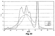
【0131】
図22は、34°の入射平行光源による反射モードにおいて用いられるELDIM EZ コントラストモデル160R(ELDIM EZ Contrast model 160R)で測定された場合の実施例1、5および17による光の反射の断面図のグラフを示している。グラフは、比較例1の場合には、ELDIMグラフでは鋭い山として観察される光源の適度に鮮やかな画像があることを示している。構造に対して設計されたXZ平面拡散を有する実施例5は、観察角度にわたって一様でないか、または平らでないゲインを形成する。これは、不完全な半径のダイヤモンドツールから生じうる。これは、明るいスポットおよび薄暗いスポットでは、一様でない明るさのディスプレイを生じることになる、実施例17は、実施例5の構造の上に体積拡散体を含み、より滑らかで、より均一な分散を生じる。
【0132】
実施例17などの30°程度のより広い視角を有するサンプルは、一般に30%または30%未満の体積拡散体層の塗布によって生じる比較的小さいゲインの減少を有する。10°未満程度の狭い視角のサンプルは、拡散体が追加されるときに、ゲインの著しい減少を有する。約60%の変化がより一般的である。
【0133】
上述の実施例5〜17は、単独のダイヤモンドビット切削ツールおよびFTSを用いて得ることができる新奇な拡散反射パターンを実証している。ダイヤモンド切削ツール面は、YZ平面断面において見られるように、主要な曲面反射ファセットおよび二次的な立上りファセットを有するプリズム状の溝を形成する。YZ平面における面の曲率は、YZ反射面において制御された拡散角度範囲を形成する。XZ平面における曲率または勾配は、XZ平面反射面において制御された拡散角度範囲を形成する。反射パターンは、極グラフにおいて連続であり、ピークおよび半幅によって形成される。
【0134】
ツール面の「反復セル」は、ツール面全体の反射光パターンを再現するツールの最小領域である。実施例5〜17において、湾曲したファセット形状およびFTS波形の勾配において不連続ではないために、反復パターンは極グラフにおいて連続である。
【0135】
上述の実施例は、2つの異なるタイプの微細複製構造に含まれている。図5および6に示されている実施例2および3は、勾配が不連続である点で接合される一般に第1の反射面および一般に立上りと呼ばれる第2の一般に未使用の面を有する実施例である。図14および18に示される実施例8、9および11は、FTSによって形成され、一般に連続的な勾配のプリズムを有する実施例である。これらの状態は、反射光の単独領域、すなわち、たとえば、図4、8、11〜13および15〜16に示されているように、反射光の極グラフに輝度の単独連続領域を生じる。
【0136】
図9に示された実施例4は、複数のファセットを有する第1の反射面を有する。2つのファセット間の境界は、不連続勾配の点として規定される。反射面における単独のファセットは反射光の極グラフにおける反射光の単独領域を形成し、反射面の複数のファセットは一般に反射光の複数の領域を形成することがわかっている。反射光の複数の領域は個別であっても、重なっていてもよい。拡散体の追加は、領域の境界を滑らかにする。
【0137】
実施例18〜29−複数の反射領域
以下の実施例18〜29は、光反射の複数の領域を形成するさまざまなマルチファセットのある微細複製構造を示している。光反射の複数の領域を形成するために、光指向微細複製構造は、不連続な勾配によって規定される複数のファセットを有する曲面をなす。各ファセットの面は光反射の結果として生じる個別領域のパターンまたは形状を決定し、すべてのファセットの和は全体の反射パターンを完成する。
【0138】
実施例1〜17において上述した実施例の大部分は、光反射の単独領域を有する反射パターンを形成する。すなわち、光指向微細複製構造の反復セルは、単独の平坦または湾曲したファセットを有する。
【0139】
図23Aに概略的に示されている実施例18は、複数の三角プリズム1040を含む構造面1014を有する光指向フィルム1010を示している。三角プリズム1040は、第1のプリズム面1042および第2のプリズム面1044を有する二等辺三角形のプリズムである。プリズム面1042、1044のそれぞれは、y軸に対して角度αをなす。このようなプリズム面をファセットまたは反射ファセットとも呼ぶことができる。第1のプリズム面1042および第2のプリズム面1044は平坦またはまっすぐである。すなわち、第1の面1042または第2の面1044のいずれに関連する曲率も本質的に存在しないことを意味している。プリズム1040、すなわち面1042、1044は、フィルム1010のx方向に沿って延在している。各プリズム1040の高さ、すなわちz方向におけるプリズム1040の寸法は、x方向に沿って一定である。
【0140】
垂直入射平行光線によって照射されるとき、実施例18のフィルム1010からの所期の光反射が、図23Bに示されている。反射光は、約2nαの極角度で0〜180°の方位角平面における2つの対称な反射を有するパターンを形成する。尚、αはプリズム1042、1044の傾斜角であり、nは任意の保護ポリマーコーティングの屈折率である。第1のプリズム面1042によって反射する光線1052は1つの反射を形成し、第2のプリズム面1044によって反射する光線1054は第2の反射を形成する。
【0141】
光線が逆行する場合には、反射パターンによって規定される方向から入射する光は、極グラフの起点(図23B)である法線方向に反射されることが分かる。このことは、これらの不透明な領域から発している一部の光が反射され、面に対して通常は垂直に位置し、観察している見ている人に達することを示している。
【0142】
図24Aおよび25Aに示されている実施例19および20は、それぞれ、湾曲したプリズム面またはファセットを有する光指向フィルムである。光指向フィルム1100として図24Aに示されている実施例19は、1つのプリズム面1142を有するプリズム1140を含む構造面1114を有する。プリズム面1142は、個別の先端または点を持たず、滑らかで連続する円弧である。光指向フィルム1200として図25Aに示されている実施例20は、プリズム1240を含む構造面1214を有する。プリズム1240は、第1のプリズム面1242および第2のプリズム面1244を有する。谷1243は、個別のプリズム1240を分離する。プリズム1140、1240および面1142、1242、1244は、フィルム1100、1200のx方向に沿って延在している。各プリズム1140、1240の高さ、すなわちz方向におけるプリズム1140、1240の寸法は、x方向に沿って一定である。
【0143】
プリズム面1142、1242、1244のそれぞれは、湾曲した切削面を有する単独のダイヤモンドビットによって形成される曲面である。あるいは、プリズム面1242および1244は、二重またはデュアルダイヤモンドビットによって同時に切削されることも可能である。各ダイヤモンドビットは、プリズム面を切削する。すなわち、プリズム面1242は第1のダイヤモンド切削ビットによって形成され、プリズム面1244は第2のダイヤモンド切削ビットによって形成されることになる。一般に、これらの二つの切削ビットは、互いに連結されてもよく、複数のプリズムピッチに等しい追加増分だけ分離されていてもよい。
【0144】
フィルム1100、1220からの垂直入射平行光に関して結果として生じる所期の光パターンが、図24Bおよび図25Bに示されている。いずれの実施例の場合も、光パターンは、極角度2nθによって0〜180°の方位角平面に沿った線である。尚、θはプリズム1142、1242、1244に対する接線の角度であり、nは任意の保護ポリマーコーティングの屈折率である。図24Bにおいて、単独の円弧を有するフィルム1100は、グラフの中心から対称に拡散する光として示されている。フィルム1200の場合には、図25Bは、グラフの中心の周囲に対称に位置する光反射の2つの個別の線を形成する2つのファセットを有する構造を示している。2つの個別の反射の間隙は、ファセット1242および1244の間の勾配の不連続性に基づいている。具体的に言えば、Δθがファセット1242および1244の交差線に垂直な経路に沿った面の角度の間の差であるとき、2nΔθに等しい。
【0145】
実施例21、22および23は、FTSの移動および平坦なダイヤモンド切削ビットによって生成される面を有するフィルムを示している。図26Aに示されている実施例21は、プリズム1340を含む構造面1314を有するフィルム1300である。プリズム1340は、第1のプリズム面1342および第2のプリズム面1344を有する。フィルム1300では、プリズム1340および面1342、1344はフィルム1300のy方向に沿って延在している点を除き、フィルム1300は、図23Aのフィルム1000と類似である。各プリズム1340の高さ、すなわちz方向におけるプリズム1340の寸法は、y方向に沿って一定であり、x方向に沿って変化する。実施例22および23のフィルム1400および1500は、この点に関して実施例21と類似である。
【0146】
図27Aにフィルム1400として示されている実施例22は、プリズム1440を含む構造面1414を有する。プリズム1440は、プリズム面1442を有する。プリズム1440および面1442は、y方向に沿って延在する。プリズム面1442は、連続正弦曲線または余弦曲線をなす。
【0147】
図28Aにフィルム1500として示されている実施例23は、プリズム1540を含む構造面1514を有する。プリズム1540は、第1のプリズム面1542および第2のプリズム面1544を有する。プリズム1540および面1542、1544は、y方向においてフィルム1500に沿って延在する。プリズム面1542、1544は、それぞれが湾曲した円弧である点を除き、図25Aにおける実施例20のフィルム1200と類似である。面1542、1544は、共に2つの円弧構成をなす。
【0148】
実施例21、22および23に関する所期の光反射パターンが、図26B、27Bおよび28Bにそれぞれ示されている。
【0149】
実施例21の場合には、垂直入射平行光によって照射されるとき、反射光は、約2nαの極角度で図26Bに示されているように、90〜270°の方位角平面において2つの対称な反射を有するパターンをなす。尚、αはプリズム面1342、1344の傾斜角であり、nは任意の保護ポリマーコーティングの屈折率である。図23Aおよび23Bの実施例18と同様に、第1のプリズム面1342によって反射する光線は領域の一方を形成し、第2のプリズム面1344によって反射する光線は第2の領域を形成する。
【0150】
光線が逆行する場合には、反射パターンによって規定される方向から入射する光は、極グラフの起点である法線方向に反射されることが分かる。このことは、これらの不透明な領域から発している一部の光が反射され、面に対して通常は垂直に位置し、観察している見ている人に達することを示している。
【0151】
垂直入射平行光は、図27Bに示されているパターンの実施例22によって反射する。垂直入射平行光は、図28Bに示されているパターンの実施例23によって反射する。いずれの実施例22および23の場合も、光パターンは、極角度2nθによって90〜270°の方位角平面に沿った線である。尚、θはプリズム面1442、1542、1544に対する接線の角度であり、nは任意の保護ポリマーコーティングの屈折率である。図27Bにおいて、単独の円弧を有するフィルム1400は、グラフの中心から対称に拡散する光として示されている。フィルム1500の場合には、図28Bは、グラフの中心の周囲に対称に位置する光反射の2つの個別の線を形成する2つのファセットを有する構造を示している。パターンが90°回転されている点を除き、これらのパターンは、実施例19および20(図24Bおよび25B)のパターンと類似である。
【0152】
実施例24〜29は、プリズムの高さがx方向およびy方向の両方に沿ってz方向において変化する複数のピラミッド状プリズムを有するフィルムの実施例である。実施例24および25はそれぞれ、フィルム1600、1700として図29A、図30Aに示されている。実施例27は、フィルム1800として図31Aに示されている。フィルム1600、1700、1800のそれぞれは、複数のピラミッド状プリズム1640、1740、1840を含む構造面1614、1714、1814を有する。
【0153】
実施例24の場合には、XZ平面およびYZ平面の両方においてまっすぐな面を有するプリズム1640は対称な二等辺プリズムである。各プリズム1640は、第1の面1641、第2の面1642、第3の面1643および第4の面1644を有する。4つの面は、頂点1645で交わる。反射光の所期の結果として生じるパターンが、図29Bに示されている。フィルム1600が平行な垂直入射光を受けるとき、光は4つの方向に分割され、反射の4つの個別領域は、極グラフの各象限に1つずつ形成される。元の光線は垂直入射平行光であり、極グラフ上のスポットまたは点として現れることから、4つの反射は相当集光される。
【0154】
図30Aの実施例25の場合には、プリズム1740は、XZ平面およびYZ平面の両方に曲面または円弧を描く面を有する対称な4つの側面を有するプリズムである。プリズム1740は、頂点1745で交わる4つの面1741、1742、1743、1744を有する。頂点1745は、実施例24のフィルム1600による頂点1645のように鋭いピークではない。正確に言えば、頂点1745は、x方向およびy方向の両方に延在する円弧の曲線の交差によって形成される相当丸みを帯びた面を有する。平行垂直入射光がフィルム1700に形成されるとき、光は4つの方向に分割され、それぞれがほぼ四角形として形成される反射の4つの個別領域が形成される。図30B参照。反射光の四角形または矩形は、反復セルを形成する4つの個別の湾曲したプリズム面1741、1742、1743、1744によって生じる。
【0155】
光線が逆行する場合には、反射パターンによって規定される方向から入射する光は、極グラフの起点である法線方向に反射されることが分かる。このことは、これらの不透明な領域から発している一部の光が反射され、面に対して通常は垂直に位置し、観察している見ている人に達することを示している。
【0156】
実施例26は、実施例25の光指向フィルムの上に配置される体積拡散体を含む。所期の光反射パターンが、図30Cに示されている。体積拡散体を含む実施例26は、体積拡散体を含まない実施例25より小さい鋭いエッジを有するより広い光反射を有する。光反射は、実施例25による反射よりさらに分散され、依然として4つの対称性を保持している。
【0157】
実施例25および26の光指向フィルムを作製する場合には、面からの切り込みおよび隆起を交互に繰り返すピラミッド状のプリズムは、x方向に沿って切削されてもよい。2つのピラミッドの間の交差線は、連続勾配を有する。「切り込み」は、ピラミッドが井戸または正の隆起したピラミッドの負部分となることを意味する。
【0158】
図31Aに示された実施例27のフィルム1800は、フィルム1800がXZ平面およびYZ平面の両方に曲面または円弧を描く面を有する対称な4つの側面を有するプリズムである点を除き、図30Aのフィルム1700と類似である。プリズム1840は、頂点1845で交わる4つの面1841、1842、1843、1844を有する。頂点1845は、鋭いピークではなく、x方向およびy方向の両方に延在する円弧の曲線の交差によって形成される相当丸みを帯びた面を有する。プリズム1840は、余弦曲線、単独円弧曲線、二円弧曲線の組み合わせによって形成される。(YZ平面における)y方向に沿って延在するとき、プリズム1840は、単独の円弧部分および二円弧部分を交互に繰り返して構成される曲線によって規定される。二円弧部分は、不連続な勾配を形成する頂点で交わる2つの単独の円弧である。2つの個別の切削通過または単独の切削通過のいずれかにおいて、2つの個別のダイヤモンドビットおよび異なる波形を同時に駆動する2つのFTSステージを用いて、Y軸断面を規定する交互の単独円弧部分および二円弧部分を切削してもよい。余弦曲線および二円弧部分の曲線の両方は、x方向においてx軸に沿って交互方式で延在する。すなわち、図31Aに示されているように、余弦曲線は一番前の曲線であり、後方の次の曲線は二円弧部分を含み、後方の第3の曲線は再び余弦曲線であり、以下同様である。ピークまたは頂点がプリズム1840の頂点1845を形成するように、y方向合成曲線のピークまたは頂点は、x方向合成曲線のピークまたは頂点と交差する。x方向における交互のピラミッド状プリズムは、実施例25および26において上述したように、ツールに切れ込みを入れたり、隆起させたりして形成されてもよい。「内部」または「外部」のプリズムによる反射光パターンは、同一である。図31Aは、4つの反復セルを示している。
【0159】
実施例27において、ピークで不連続な勾配を有する曲線によって二円弧部分を置換することも可能である。そのような曲線の一例は、ゼロの両側面に20°などの対称な部分が除去される余弦曲線である。同様に、図18の内/外の円弧を交換するなど、別の連続曲線によって連続的なFTS余弦曲線を置換することも可能である。
【0160】
平行垂直入射光がフィルム1800によって反射されるとき、光は4つの方向に分割され、図31Bに示されているように、4つの象限を通って連続する中空または環状の四角形の反射パターンを共に規定する4つの矩形の反射領域が得られ、4つの回転対称を形成する。
【0161】
光線が逆行する場合には、反射パターンによって規定される方向から入射する光は、極グラフの起点である法線方向に反射されることが分かる。このことは、これらの不透明な領域から発している一部の光が反射され、面に対して通常は垂直に位置し、観察している見ている人に達することを示している。
【0162】
実施例28は、実施例27の光指向フィルムの上に体積拡散体を含む。所期の光反射パターンが、図31Cに示されている。体積拡散体を含む実施例28は、体積拡散体を含まない実施例27より小さい鋭いエッジを有するより広い光反射を有する。実施例28による光反射は、実施例27による反射よりさらに分散され、依然として回転対称性を保持している。
【0163】
体積拡散体を有するフィルム1800または体積拡散体を含まないフィルム1800などの回転対称性の光指向フィルムは、光指向ディスプレイにおけるフィルムの配向に対する感度が小さいために望ましい。たとえば、照射品質を妥協することなく、光指向フィルム1800は、光指向ディスプレイの最適な配向角度からたとえば20°だけ回転(または位置ずれ)していてもよく、そのような自由度がさらなる4つの配向対称性に重なる。
【0164】
実施例27および28において、反射光パターンの中空または環状形状およびその4つの回転対称性は、連続勾配および不連続勾配の特定の選択利用に起因する。n個の回転対称または複数の包囲された暗領域などのさらに複雑なパターンも、さらに複雑なツール構造を与えるために考慮することが可能である。
【0165】
ここで図32Aを参照すると、実施例29の光指向フィルム1900が示されている。フィルム1900は、空隙1950によって分離されるプリズム1940から構成される構造面1914を有する。プリズム1940は、第1の面1942および第2の面1944を有する。面1942、1944は、隆起ピーク1945で交差する。
【0166】
実施例29の反射光パターンは、0〜180°の方位角平面において2つの対称な反射を有する点で、図23Aおよび23Bの実施例18の反射光パターンと類似である。しかし、実施例29はまた、空隙1950による反射によって生じるグラフの中心に位置する中心反射領域も含む。実施例28は実施例18(図23Aおよび32B)の2つのファセット構造によって構成されるのと同一の態様で、実施例29などの3つのファセット構造に基づいて形成される一連の複雑なパターンを想定することも可能である。
【0167】
実施例18〜29のそれぞれは、体裁のための欠陥を隠し、さらなる拡散を生じるために、基本のプリズム面の上に重ね合わせられたFTS雑音を含むことも可能であることを理解されたい。
【0168】
本発明は、上述の特定の実施例に限定されると考えるべきではなく、むしろ添付の特許請求の範囲に記載されているように、本発明のすべての態様を網羅するものと理解すべきである。本発明が適用可能であると思われるさまざまな修正、等価な工程のほか、さまざまな構造および構成は、本願明細書を検討すれば、当業者には容易に明白となるであろう。特許請求の範囲は、そのような修正および装置を包含するものとする。
【図面の簡単な説明】
【0169】
【図1A】光指向構成を組み込んだディスプレイ装置の概略断面図である。
【図1B】図1Aのディスプレイ装置の光方向構成の一部の拡大概略断面図である。
【図2A】ディスプレイ装置の見ている人によって見られている光の分散を量的に示すために用いられる座標系の概略図である。
【図2B】構成のための相対的な軸を示す光指向フィルムの概略斜視図である。
【図2C】光指向フィルムを作製するために用いることができる円筒ツールの概略平面図である。
【図3】従来の構造層を有する従来の光指向構成の概略断面図である。
【図4】34°の入射平行光による反射モードで用いられるELDIM EZ Contrast model 160Rで測定した場合の図3に示された比較例1の光指向フィルムの反射光強度のグラフ図である。
【図5】本発明の第1の態様による光指向構成の第1の実施形態の概略断面図である。
【図6】本発明による光指向構成の第2の実施形態の概略断面図である。
【図7】34°の入射平行光による反射モードで用いられるELDIM EZ Contrast model 160Rで測定した場合の図6に示された実施例3Aの光指向フィルムの反射光強度のグラフ図である。
【図8】34°の入射平行光による反射モードで用いられるELDIM EZ Contrast model 160Rで測定した場合の図6に示された実施例3Bの光指向フィルムの反射光強度のグラフ図である。
【図9】本発明による光指向構成の第3の実施形態の概略断面図である。
【図10A】本発明による光指向フィルムの第4の実施形態の概略斜視図である。
【図10B】本発明による光指向フィルムの第5の実施形態の概略斜視図である。
【図11】34°の入射平行光による反射モードで用いられるELDIM EZ Contrast model 160Rで測定した場合の実施例5の光指向フィルムの反射光強度のグラフ図である。
【図12】34°の入射平行光による反射モードで用いられるELDIM EZ Contrast model 160Rで測定した場合の実施例6の光指向フィルムの反射光強度のグラフ図である。
【図13】34°の入射平行光による反射モードで用いられるELDIM EZ Contrast model 160Rで測定した場合の実施例7の光指向フィルムの反射光強度のグラフ図である。
【図14】本発明による光指向構成の第6の実施形態の概略断面図である。
【図15】34°の入射平行光による反射モードで用いられるELDIM EZ Contrast model 160Rで測定した場合の実施例8の光指向フィルムの反射光強度のグラフ図である。
【図16】34°の入射平行光による反射モードで用いられるELDIM EZ Contrast model 160Rで測定した場合の実施例9の光指向フィルムの反射光強度のグラフ図である。
【図17】本発明による光指向構成の第7の実施形態の概略断面図である。
【図18】本発明による光指向構成の第8の実施形態の概略断面図である。
【図19】走査型電子顕微鏡の下で見た場合の本発明による光指向構成の第9の実施形態の概略断面図である。
【図20】走査型電子顕微鏡の下で見た場合の本発明による光指向構成の第10の実施形態の概略断面図である。
【図21】本発明の別の態様による光指向構成の概略上部平面図である。
【図22】34°の入射平行光による反射モードで用いられるELDIM EZ Contrast model 160Rで測定した場合の実施例1、5および17の光指向フィルムの反射光強度のグラフ図である。
【図23A】本発明による光指向フィルムの第11の実施形態の概略斜視図である。
【図23B】直交入射平行光で照射した場合の実施例18の光指向フィルムの反射光強度の概略グラフ図である。
【図24A】本発明による光指向フィルムの第12の実施形態の概略斜視図である。
【図24B】直交入射平行光で照射した場合の実施例19の光指向フィルムの反射光強度の概略グラフ図である。
【図25A】本発明による光指向フィルムの第13の実施形態の概略斜視図である。
【図25B】直交入射平行光で照射した場合の実施例20の光指向フィルムの反射光強度の概略グラフ図である。
【図26A】本発明による光指向フィルムの第14の実施形態の概略斜視図である。
【図26B】直交入射平行光で照射した場合の実施例21の光指向フィルムの反射光強度の概略グラフ図である。
【図27A】本発明による光指向フィルムの第15の実施形態の概略斜視図である。
【図27B】直交入射平行光で照射した場合の実施例22の光指向フィルムの反射光強度の概略グラフ図である。
【図28A】本発明による光指向フィルムの第16の実施形態の概略斜視図である。
【図28B】直交入射平行光で照射した場合の実施例23の光指向フィルムの反射光強度の概略グラフ図である。
【図29A】本発明による光指向フィルムの第17の実施形態の概略斜視図である。
【図29B】直交入射平行光で照射した場合の実施例24の光指向フィルムの反射光強度の概略グラフ図である。
【図30A】本発明による光指向フィルムの第18の実施形態の概略斜視図である。
【図30B】直交入射平行光で照射した場合の実施例25の光指向フィルムの反射光強度の概略グラフ図である。
【図30C】直交入射平行光で照射した場合の実施例26の光指向フィルムの反射光強度の概略グラフ図である。
【図31A】本発明による光指向フィルムの第19の実施形態の概略斜視図である。
【図31B】直交入射平行光で照射した場合の実施例27の光指向フィルムの反射光強度の概略グラフ図である。
【図31C】直交入射平行光で照射した場合の実施例28の光指向フィルムの反射光強度の概略グラフ図である。
【図32A】本発明による光指向フィルムの第20の実施形態の概略斜視図である。
【図32B】直交入射平行光で照射した場合の実施例29の光指向フィルムの反射光強度の概略グラフ図である。【Technical field】
[0001]
The present invention relates to an optical film and a method for producing the same. More specifically, the present invention relates to an optical film including a layer having a micro-replicated structure.
[Background Art]
[0002]
Reflective imaging devices, also known as special light modulators, form visible images by locally altering the reflection of light. One useful device of this type is a liquid crystal display or LCD, in which the light incident on the display is provided by electronically processed pixels of liquid crystal material sandwiched between polarizers in an image-wise manner. Is either transmitted, reflected or blocked, thereby forming a visible image on the display.
[0003]
LCDs are often illuminated by light incident on one major surface of the LCD (called the back surface) and exit from the other surface, the front surface where the viewer is. It is also possible to illuminate the LCD from the front, i.e. the viewing side, with a suitable reflector to create an image illuminated by the ambient light reflected by the reflector (commonly referred to as a back reflector). . LCDs illuminated in this manner are commonly referred to as reflective LCDs or RLCDs.
[0004]
Both specular and diffuse back reflectors have been used, each having certain disadvantages. Specular back reflectors can present a metallic image appearance and reflect images of objects located behind or on top of the viewer, creating an unacceptably limited viewing angle And can vary depending on the particular ambient light conditions. In addition, the specular reflector reflects incident light such that the head of the viewer may block the incident illumination needed for best display. Diffuse reflectors, on the other hand, have the disadvantage of inefficient use of light in that they can diffuse light to locations where the viewer is unlikely to be, so they illuminate from more desirable display positions. You will remove the light. These disadvantages are summarized in U.S. Pat. No. 4,298,249, which discloses a method for tilting an incident light to reflect the incident light at an angle such that the display can be viewed from a more suitable location. In addition to a back reflector having a reflecting surface stripe formed, a diffusing surface structure is provided. Similarly, U.S. Patent No. 6,204,903 discloses reflective and partially reflective surfaces having various structural shapes that direct reflected light in a particular direction. To accommodate a variety of light conditions, U.S. Pat. No. 5,128,787 discloses a reflector having variously angled structures to reflect light from various light sources to a desired viewing position. Is disclosed. The disclosed structure also has the advantage of reducing the effects of glare because the image can be viewed from a location outside of the area that receives the undesired specular light from various surfaces and boundaries of the display.
DISCLOSURE OF THE INVENTION
[Problems to be solved by the invention]
[0005]
The present invention provides a microstructured reflective surface that reflects incident light at a predetermined angle and creates a dispersion of the reflected light in a particular direction. The microstructured surface has a general overall shape with a small tilted reflective microstructure built on the surface. The graded microstructure has a longitudinal variation at a height or altitude defined by a predetermined periodic height or altitude. The height may vary according to a constant period, a variable but deterministic period, an irregular period, or a combination thereof.
[Means for Solving the Problems]
[0006]
A suitable tool for making a microstructured surface according to the present invention is a liquid composition that can be diamond turned into a desired pattern on a cylindrical blank composed of a suitable metal such as hard copper and cured on a film backing. Can be fabricated by using this cylinder as a casting tool to form a coating on the microstructured layer. A piezoelectric element built into the diamond tool holder can add a depth function to the diamond turning process. This type of tool holder is commonly called a high speed tool servo or FTS. In general, it may be called a high-speed servo tool. The signals used to drive the FTS may include single or multiple frequency waves, signals from noise generators, and any other signals that have been found useful. For example, the signal may be filtered to limit a varying frequency range or spectral waveform at varying heights. In general, the signals that can be used to generate a depth function are limited only by the suitability of a particular signal in creating a useful microstructure. Because of the relative simplicity of generating a signal for use in the present invention, it is highly empirical to determine the appropriate signal to create the various heights that produce the desired optical effect. It is possible to take an approach.
[0007]
As used herein, the term "reflective optical surface" includes both highly reflective surfaces, such as mirrors, and optical surfaces that only partially reflect and transmit a significant amount of light. This type of partial reflector is commonly referred to as a transflective optical surface. The reflective surfaces of the present invention can form reflections, for example, by metallization with a suitable metal such as silver. Also, protective coatings and other surface conditioning coatings may be incorporated.
[0008]
The optical film having a reflective surface of the present invention can be designed to reflect light in the direction of the effective range, such that the available light is used more efficiently and the glare effect can be avoided. Is useful as a back reflector for LCDs because it can form a strictly controlled distribution of.
[0009]
In addition to the microstructure defined by the tilt angle and the depth function, additional surface treatments such as chemical etching of the tool can be used to form a diffuse or other directional component to the reflected light distribution. . Plating the tool may be useful in improving the durability of the tool and the surface quality of the microstructure product.
[0010]
In particular, in one aspect, the invention relates to a light directing film having an x-axis, a y-axis, and a z-axis, the film having a first structural surface and an opposing surface. The structural surface has a plurality of prism structures thereon, the prism structures extending substantially along the x-axis, with gaps along the y-axis between adjacent prism structures. The structure also has a height along the z-axis, and the height of the prism structure varies along the x-axis with a repetition period.
[0011]
In another aspect, the present invention is a microreplicated light-reflective film, comprising a plurality of prism structures having a length, each of the plurality of prism structures having a height that varies along the length in a repeating cycle. The present invention relates to an optical element including a film. A metal film layer may be present on the film.
[0012]
The present invention is also an article made using a programmable cutting tool that has an x-axis, a y-axis, and a z-axis, wherein the plurality of structures extend substantially along the x-axis. Wherein the plurality of structures have a gap along the y-axis between adjacent prismatic structures, have a height along the z-axis, and the height of the structures varies along the x-axis in a repeating pattern Related to goods.
[0013]
According to the present invention, a method for making a film with a reflective structure includes machining a master tool from a blank using a cutting tool, the cutting tool being movable in x, y, and z directions. is there. The machining steps include contacting the cutting tool with the blank, moving the blank and / or the cutting tool relative to each other in the x direction to cut the blank, and relative to each other in the y direction to cut the blank. Moving at least one of the blank and the cutting tool; and moving at least one of the blank and the cutting tool with respect to each other in the z-direction to cut the blank. In this master tool for machining, a structured film is produced and then the structured film is provided with a reflective coating.
[0014]
The method of the present invention provides a structured film that is more dense, precise or precise than a film made using methods such as chemical etching, bead blasting or other stochastic surface conditioning techniques. Methods such as chemical etching, bead blasting or other stochastic surface conditioning techniques cannot accurately reproduce the precise shape from one prism face to the next, for example to 0.001 micrometers. Even less than 0.0001 micrometers is even more so.
[0015]
The present invention will be more completely understood in consideration of the following detailed description of various embodiments of the invention in connection with the accompanying drawings.
BEST MODE FOR CARRYING OUT THE INVENTION
[0016]
The present invention relates to an optical film that improves the utilization of light in a reflective liquid crystal display (RLCD) by precisely forming a pattern of light that is diffusely reflected by the RLCD. In particular, by designing the surface features of the RLCD's back reflector to reflect in a particular direction, the dispersion of the reflected light is formed as desired for better uniformity and brightness. Is done.
[0017]
As used herein, an optical film is a film having a structural or prismatic surface that includes a structure that reflects light at a desired angle to RLDC.
[0018]
A
[0019]
This specification describes a
[0020]
Referring again to FIG. 1A, the peripheral
[0021]
Most of the incident light passes through the
[0022]
Referring to FIG. 1B, which is an enlarged view as compared to FIG. 1A, a light directing arrangement 28, shown as a structural layer, is formed to advance the image generated by the
[0023]
In FIG. 1B, an incident light beam 32 is incident on the display device represented by line 33 at an angle a from the normal. The normal is the direction perpendicular to the display surface. The incident light beam 32 is refracted by various components of the
[0024]
The particular design of the light directing arrangement 28 can control the range of viewing angles at which an image can be viewed and the range of viewing angles at which peak brightness occurs.
[0025]
In FIG. 1A, the peak image angle or optimal viewing angle is substantially orthogonal to the display, as represented by image ray 38. As a result, a person viewing the
[0026]
As can be seen in FIG. 1B, the light directing arrangement 28 is a prismatic light directing film with a structure having a smooth surface 31 and a structured surface 33. This will be described in detail below with reference to the drawings. The smooth surface 31 is on a side different from the rear of the
[0027]
The present invention relates to designing a light directing configuration to produce a desired image beam intensity distribution over a desired range of angles. Depending on the particular configuration of the prismatic light directing film, the direction and angular range of the reflected beam can be changed. The coordinate system used to quantify the light variance seen by the viewer of the RLCD is shown in FIG. 2A. In FIG. 2A, point "P" may be a viewer, a photometer for measuring brightness, a light source, or some other item. Point “P” has spherical coordinates θ called azimuth or simply azimuth, φ called polar angles, and ρ called radial coordinates. In FIG. 2A, when viewed by a viewer, point 29 is a point on
[0028]
When the physical instance is characterized by an “ELDIM EZ Contrast model 160R” photometer, one can see the particular effect of beam steering. This photometer is a polarization photometer used in reflection mode with 34 ° incident parallel light. The ELDIM photometer measures reflection brightness as a function of θ and φ and has a 360 ° azimuthal range over polar angles ranging from 0 ° (normal to the film) to 80 ° (10 ° from the plane of the film). Data is represented by coordinates over. The optical gain is obtained by normalizing with the same luminance with respect to the luminance of the white Lambert standard measured under the same conditions. In FIGS. 4, 7, 8, 11, 12, 13, 15 and 16, graphs using this coordinate system can be seen. θ is expressed as a frequency around the circular graph, starting at the top of the graph and rotating counterclockwise, and φ is expressed by the radial distance from the center of the graph.
[0029]
FIG. 2B is a perspective view of a general light directing configuration showing a prism structure. The following example is described using the axes shown in FIG. 2B. The “x-axis” or “x-direction”, also referred to as the longitudinal direction of the structure, is in the direction of the ridge or microstructure. The "y-axis" or "y-direction" is orthogonal to the x-axis and traverses the plane of the structure, so that the x-axis and the y-axis define a reference plane 29 and define the overall shape of the light directing element 28. The “z-axis” or “z-direction” is perpendicular to the plane formed by the x-axis and the y-axis and extends from the back of the light directing element 28 to the front.
[0030]
Conveniently, a light directing configuration having structure 33 can be made using a cylindrical casting tool of the type depicted in FIG. 2C. In FIG. 2C, a
[0031]
The light directing film of the present invention may be of any formable material and is typically transparent. UV-polymerizable materials, including acrylics and polycarbonates, are preferred materials. In general, UV polymerizable compositions for making light directing films include vinyl monomers, such as, for example, alkyl styrene monomers such as methyl styrene, and various comonomers and / or oligomers. In one example, the composition comprises each of a bisphenol A type epoxy diacrylate, a novolak type epoxy acrylate, and a vinyl monomer including an alkyl styrene (eg, methyl styrene). Such compositions are considered "epoxy acrylates". An initiator may be added to provide a source of free radicals to initiate polymerization of the composition into the polymer structure.
[0032]
One example of a preferred UV-polymerizable epoxy acrylate composition for use in light directing films is the following components listed by weight percent in a range: bisphenol A epoxy diacrylate (55-80%), acrylated epoxy (1 to 10%), methylstyrene (5 to 25%), a photopolymerization initiator (0.25 to 5%) (such as "Lucirin TPO") and a fluorine-based surfactant (0.1 to 10%). 0.3%). Further, the composition can include up to about 5% by weight of a second photoinitiator, such as "Irgacure 184". Further details regarding these preferred UV-polymerizable compositions are described in U.S. patent application Ser. No. 09 / 425,270, filed Oct. 22, 1999 (Fong). This patent specification is incorporated herein by reference.
[0033]
A reflective coating can be applied to the structured film. The reflective coating may be opaque and may be a metal such as silver, chromium, nickel, aluminum, titanium, aluminum-titanium alloy, gold, zirconium, platinum, palladium, aluminum-chromium alloy, rhodium or a combination thereof. Good. A preferred reflective metal coating is silver. The reflective coating may be continuous or discontinuous. A discontinuous coating may be achieved by applying a discontinuous coating or by removing a portion of the continuous coating.
[0034]
Also, additional layers such as an adhesion promoting layer, a diffusion barrier layer and a corrosion resistant layer may be used to improve the performance and durability of the reflective metal coating. One example of a preferred corrosion resistant layer is taught in PCT published patent application WO 01/31393 (Gardner et al.). This patent specification is incorporated herein by reference.
[0035]
The diffuser layer is preferably applied over the structured film to hide film defects and eliminate moiré effects. Since the light directing film of the present invention diffuses light sufficiently for the prism structure, the diffuser layer does not need to diffuse reflected light. One example of a diffuser layer is a polymethyl-methacrylate polymer with added polymer beads or glass beads.
[0036]
Polymer hosts or carriers generally have a refractive index of 1.4 to 1.5, but may be larger or smaller. Beads, whether polymeric or glass, generally have a refractive index of 1.35 to 1.7. The difference in refractive index between the bead and the host or carrier polymer is a deterministic property during bead and polymer selection. For most applications, the difference in refractive index is preferably from 0.01 to 0.2, and more preferably from 0.02 to 0.1.
[0037]
The average diameter of the beads is generally between 0.5 and 20 micrometers, and for use in handheld display devices, the preferred bead diameter is between 2 and 5 micrometers. The amount of beads added to the polymer depends on the average bead diameter. A smaller diameter bead will add a smaller bead volume, and a larger diameter bead will add a larger volume. As an example, if the difference in the refractive indices is about 0.05 and the bead diameter is about 5 micrometers, a useful addition is 1% to 10%.
[0038]
When the bead is added quite densely, the diffuser layer can disperse light from distant sources to create uniform bright back reflections in the absence of a recognizable image of the source, resulting in defects and artifacts. Hide. PCT published patent application WO 97/01610 (Goetz et al.), Which is hereby incorporated by reference herein, discloses a method for masking defects and other artifacts. Teaches a light-diffusing adhesive that can be used with the film.
[0039]
Another technique for creating irregular scattering includes applying a matte finish to the tool. After machining the grooves, a matte finish can be achieved by acid etching, ion plating or bead blasting the structured copper tool.
[0040]
Absorbing dyes or pigments can be added to the composition or other layers in the light directing configuration to change the color of the display. For example, when viewed in ambient light, silver metal films often have a slightly yellow appearance. Absorbing dyes can be added to the construction to compensate for the yellow appearance and form an achromatic reflector.
[0041]
Applying the polymerizable composition to a mold having a plurality of cavities between the substrate and the tool or having the inverse shape of the prism, polymerizing the composition under ultraviolet light, and then separating the sheet from the tool. Light directing films can be made by a variety of different methods known in the art. Other methods for forming prism structures are known and may be used in the present invention. Due to the small size of the prism, the process for producing a three-dimensional structure is often referred to as "fine replication". See, for example, U.S. Pat. No. 5,183,597 (Lu) for further information on microreplication of three-dimensional structures. This patent specification is incorporated herein by reference.
[0042]
Tools for forming a prism are known, for example, from the known diamonds disclosed in published PCT patent application WO 00/48037, which is hereby incorporated by reference. It may be made by a turning technique. Generally, master tools are made by subjecting a cylindrical blank, known as a roll, to diamond turning. The surface of the roll is typically made of hard copper, but other materials may be used. The prism structure is formed in a continuous pattern around the roll. In a preferred embodiment, the grooves are formed by a technique known as threading. In threading, a single continuous groove is cut on the roll (in the x-direction) while the diamond bit is moved in a direction (y-direction) that translates into the turning roll. The distance between adjacent cuts is called "pitch". The diamond bit is moved at a constant speed to form a structure with a constant pitch.
[0043]
Common diamond turning techniques are generally known in the art. See, for example, PCT published patent application WO 00/48037. For details, refer to FIGS. 7 and 9 and the description thereof. This published patent describes various devices and methods that can be used to make master tools from rolls or drums. The entire disclosure of which is incorporated herein by reference.
[0044]
An apparatus used in the method for producing a light directing film of the present invention includes a high-speed servo tool. As disclosed in WO 00/48037, a high speed tool servo (FTS) is a solid state piezoelectric element that rapidly adjusts the position of a cutting tool. One type of FTS is known as PZT. The FTS takes into account the principal axes of movement of the cutting tool in the y and z directions and also makes vibrations or other minor adjustments in the y and z directions. In this case, where the cylinder is cut, movement in the x-direction is provided by rotation of the workpiece. If present, the vibration is generally superimposed on the movement of the main cutting tool. Additionally or alternatively, the cutting tool may be pivoted or rotated about the x-axis during machining to provide yet another feature.
[0045]
In another embodiment, the z-direction of a diamond cutting tool is used to form a ridge, for example, by driving an FTS with a signal formed by a periodic ramp function to form a series of facets. Movement can be used. Due to the limitations of the frequency response of the FTS, the transition between the top of one ridge and the bottom of the next ridge may be somewhat curved. Such a tilt function will, according to the invention, form a raised structure which forms a net change in the direction of the reflected light. When cutting is performed in this manner, the longitudinal direction of the prism structure is parallel, rather than perpendicular, to the axis of rotation of the tool being cut. Furthermore, the ridges may be continuous or synchronized throughout the tool, since it is not necessary to synchronize from one rotation of the cylinder to the next, or more precisely, the ridges may be asynchronous. There may be. As a result, the appearance of the illumination of the display when viewed by a viewer may be improved. The curved transition area of the casting tool may also serve to improve the appearance of the RLCD. To form additional light directing features, the diamond cutting tool may be provided with a curve or other suitable cutting profile to further improve the reflected light distribution.
[0046]
The prism structure may be formed by a method other than the above. For example, the structure of the master tool may be transferred from a master tool to another medium, such as a belt or web of polymeric material, by a casting cure step from the master tool to create the fabrication tool. The fabrication tool is then used to create a prism structure. Other methods, such as electroforming, may be used to duplicate the master tool. Another alternative for making light directing films is to directly cut or machine the transparent material to form a prismatic structure.
[0047]
The prism structures and methods of the present invention are limited only by the signals that can be generated, the frequency response of the electronics, the mechanical properties of the FTS actuator and the tool surface.
[0048]
Chemical etching, bead blasting or other stochastic surface conditioning techniques typically produce sharp, precise prismatic structures and feature widths desirable to obtain the light diffusing properties provided by the cutting tool using the methods of the present invention. It is not possible. Such an unacceptable method results in highly accurate repetitive structures such as the present invention due to the inherent inaccuracies and non-repeatability associated with chemical etching, bead blasting or other stochastic surface conditioning techniques. It cannot be formed.
[0049]
The present invention is further described and illustrated in the following examples. The examples are illustrative of the invention and should not be construed as limiting its scope in detail. It is to be understood that throughout the examples and the remainder of the specification, the terms "micrometer", "micron" and "μm" are used interchangeably.
【Example】
[0050]
The light directing films of the examples were made by microreplicating a UV-sensitive epoxy acrylate resin into a tool cut with a diamond cutter or bit to form a faceted profile. The epoxy acrylate resin was on the tool and a 5 mil (127 micrometer) PET substrate was bonded to the exposed surface of the resin. After the epoxy acrylate resin was polymerized by UV light, the resulting light directing film was removed from the tool.
[0051]
The master tool for each of the examples was made by machining a copper sheet or blank formed into a cylinder with a diamond tip cutting tool. The cutting tool was lowered onto the copper blank in the z-direction to begin the machining process. The cylinder was rotated about its central axis, moving the cutting tool in the x direction. A spiral groove is formed in the cylindrical surface to move the cutting tool along the surface of the cylinder in the y-direction. In some embodiments, the diamond cutting tool was moved in the z-direction by an FTS ("fast tool servo" or "fast servo tool"). The machined copper sheet was removed from the cylinder and used to make a light directing film.
[0052]
Example 1 Comparative Example
FIG. 3 is an enlarged cross-sectional view of a first embodiment of a light directing configuration 100 including a conventional light directing film 110. FIG. An example of such a film is the Minnesota Mining and Manufacturing Company (3M) under the trade name “Tilted Mirror Film 6.3”. Available from This view of the light directing film 110 is similar to the orientation shown in FIG. 1B, with the y-axis extending through the structure from left to right in the drawing and the z-axis extending from top to bottom in the drawing. The x-axis extends into the page.
[0053]
The light directing film 110 has a smooth surface 112 and a structured surface 114. The structural surface 114 includes a plurality of triangular prisms 140, each having a first prism surface 142 and a second prism surface 144, with alternating valleys 143 and peaks 145. First prism surface 142 and second prism surface 144 together define the pitch or period of light directing film 110.
[0054]
In this embodiment, the light directing film 110 is defined by a repeating arrangement of angular prisms 140. The pitch of the repeating prism 140 that measures valley 143 to valley 143 or valley 145 to valley 145 is generally 10 μm to 100 μm, and more preferably about 30 μm to 80 μm. In this embodiment, the light directing film 110 has a pitch of 50 micrometers. That is, the length in the y-direction between the repeating peaks 145 is 50 micrometers.
[0055]
First prism surface 142 is commonly referred to as a “facet” or “reflective facet” because most of the light reflected by light directing configuration 100 is reflected by first prism surface 142. In this embodiment, the first prism surface 142 has a height of 6 ° from the y direction. This is also called the mirror angle. It should be understood that angles other than 6 ° can be used. Generally, an angle of 0-30 ° is used, preferably 5-9 °.
[0056]
Each prism 140 has a peak angle or included angle defined by a first prism surface 142 and a second prism surface 144. Each peak 45 has the same peak angle of about 86 °.
[0057]
The light directing film 110 is manufactured by the above-described technique, and is disposed on the substrate 120. More specifically, the smooth surface 112 of the light directing film 110 is disposed with respect to the substrate 120. An adhesive may be used to fix the light directing film 110 on the substrate 120. Alternatively, the light directing film 110 may be bonded on the substrate 120 using the same material that forms the prism 140. In some embodiments, substrate 120 is a substrate used during a micro-replication process.
[0058]
The overlying prism 140 is a reflective metal coating 130 and is disposed on the structured surface 114 of the light directing film 110. The reflective metal coating may be silver or any other useful coating.
[0059]
The overlying metal coating layer 130 is a diffuser layer 135, such as a polymethyl-methacrylate polymer with added polymer beads or glass beads. Since the diffusion caused by the diffuser layer 135 is rotationally symmetric about the peak of the light reflected by the light directing film 110, the width of the diffusion in the YZ plane is the same as the width in the XZ plane.
[0060]
Specific prism and facet dimensions for Comparative Example 1 are given in Tables 1 and 2 below. All measurements are given in micrometers. The light reflectance of Comparative Example 1 was measured by an ELDIM EZ contrast model 160R used in a reflection mode with 34 ° incident parallel light. FIG. 4 is a result graph. FIG. 4 shows a sharp glare peak at 34 ° and a broader back-reflected peak centered at 14 °. Overall, the reflected light has a higher intensity at the center and is shown as a steep peak that gradually decreases until no reflected light is measured.
[0061]
The light directing configuration of the present invention differs from the sample of Comparative Example 1 in that the light directing configuration includes a light directing film and the light reflection is guided and manipulated by a prism to obtain a desired light dispersion. In most cases, a flat or top-hat variance of light intensity is desired, rather than a pointed or bell-shaped variance. This is achieved when a collimated beam of light is scattered by a surface with constant brightness within a certain angular width centered in the direction also determined by the prism features. The beam steering characteristics may be biased to a reflection angle offset from the glare direction by any suitable amount, such as 0-45 °.
[0062]
Diffusion in the YZ plane
Various techniques can be used to form the desired prismatic surface. For example, the structures can be formed such that the facet angle of each structure is not the same as the adjacent structure. By changing the facet angle, either continuously or row by row, the reflectivity of the light by the light directing film is changed, creating diffuse reflection in the YZ plane over a wide range of angles.
[0063]
Example 2-Variable facet or prism angle
FIG. 5 is a cross-sectional view of a light directing configuration 200 including a light directing film 210 according to one aspect of the present invention. This view of the light directing film 210 is similar to the orientation shown in FIG. 2, with the y-axis extending through the structure from left to right in the drawing and the z-axis extending from top to bottom in the drawing. The x-axis extends into the page.
[0064]
The light directing film 210 has a smooth surface 212 and a structured surface 214. The structural surface 214 forms a plurality of prisms 240 having a first prism surface 242 and a second prism surface 244 defining valleys 243 and peaks 245. First prism surface 242 and second prism surface 244 form a set of surfaces that define the composite. Generally, first prism surface 242 is used to reflect light, and second prism surface 244 does not contribute to the reflection or direction of light. The smooth surface 212 of the film 210 is adjacent to the substrate 220. Overlying light directing film 210 is metal coating 230 and diffuser layer 235.
[0065]
Unlike the prism 140 of the light directing film 110 of FIG. 3, the prisms 240 are not all the same. See prisms 251, 252, 253, 254. Prism 251 is different from prism 252, and prism 252 is different from prism 253. The same applies hereinafter. It should be understood that not all prisms of the light directing film 210 are different from all other prisms of the light directing film 210. Strictly speaking, it is desirable that the prism be different from the adjacent prism. Referring to FIG. 5, the prism 252 is different from the adjacent prism 251 and is different from the adjacent prism 253. Preferably, there are at least two prisms between two similar prisms, and more preferably, there are at least four prisms between two similar prisms. To optimize the visibility of visible patterns, it may be advantageous to cluster groups of prisms in a particular pattern or order.
[0066]
The prisms differ at least in that the reflective facets or first prism faces 242 have different slopes, thereby increasing light diffusion. The slope of the first prism surface 242 is generally measured from the smooth surface 212. The first prism surface 242 of the various prisms generally varies in length with respect to the inclination of the first prism surface 242. In most cases, the peaks 245 of the prism are equidistant from the smooth surface 212, but in some cases, the heights of the adjacent peaks 245 are different, as shown in FIG. Is also good.
[0067]
The diffuser layer 235 is a low density diffuser such as a polymethyl-methacrylate polymer with added polymer beads or glass beads 236. The diffuser layer 235 has fewer beads than the diffuser layer 135 of the light directing configuration 100, hides defects and artifacts, and incorporates multiple reflection peaks created by varying prism angles.
[0068]
By shaking the diamond cutting bit used to make the master tool, by high frequency periods or irregular movement, to create a surface with more optical diffusion, various angles in the YZ plane Can be formed. The variable prism angle forms a diffusion in the YZ plane. Such a diffusion is superimposed on the diffusion from the volume diffuser layer 235, giving an additional degree of freedom to identify the width of the diffusion in the XZ and YZ planes.
[0069]
In another embodiment, the master tool can be cut by a shaped diamond cutting bit, resulting in a non-flat or non-straight bit shape. Alternatively or additionally, the tool can be cut by multiple passes, with the cutting bit being placed at a different angle and at a different position than in the previous pass. The resulting uneven facets form beam steering effects and controlled light diffusion in the YZ plane, adding to the irregular diffusion of the diffuser layer. The curved or non-straight cutting edges of the diamond bit or cutter form a variable gradient that is desirable for light diffusion. Furthermore, the exact shape of the cutting edge determines the diffusion distribution.
[0070]
Examples 3A and 3B-Curved facets, non-linear facets
FIG. 6 is a cross-sectional view of a light directing configuration 300 according to another aspect of the present invention. With the y-axis extending across the structure from left to right in the drawing and the z-axis extending from top to bottom in the drawing, this view of the light directing configuration 300 and the light directing film 310 has the orientation shown in FIG. Is similar to The x-axis extends into the page.
[0071]
Light directing configuration 300 includes a light directing film 310 having a smooth surface 312 and a structured surface 314. Light directing film 310 includes a plurality of prisms 340 having a first prism surface 342 and a second prism surface 344 defining valleys 343 and peaks 345. The smooth surface 312 is adjacent to the substrate 320. The overlying light directing film 310 is a metal coating 330 and a diffuser layer 335 with low integration glass or polymer beads 336 to cover artifacts and defects.
[0072]
First prism surface 342 has a curvature associated with the surface, rather than a linear surface such as surface 142 in FIG. 3 and surface 242 in FIG. The angle of the curved surface extends from a few degrees to several degrees around the average surface angle. That is, the line drawn with a tangent to the first prism surface 342 is at an angle of 0 to 30 ° with respect to the smooth surface 312, and is usually 4 to 8 °. The curved first prism surface 342 forms a reflective facet that can be used to weight the reflected light into shaped lobes. Alternatively, the curved first prism surface 342 may be configured to form a square reflection distribution.
[0073]
Example 3A is only the light directing film 310, and Example 3B has a coating applied on the light directing film 310, and the diffuser layer 335 has a 6% volume integration polymer bead. Specific prism and facet dimensions for Examples 3A and 3B are given in Tables 1 and 2 below.
[0074]
Examples 3A and 3B were characterized by an ELDIM EZ Contrast model 160R used in reflection mode with a 34 ° incident collimated light source, and the resulting graphs are shown in FIGS. 7 and 8, respectively. Have been.
[0075]
In the case of Example 3A, which is similar to Example 2 above, the non-linear facets form a diffusion in the YZ plane, as shown in FIG. As can be seen in FIG. 8, such a diffusion is superimposed on the diffusion from the volume diffuser layer 335, giving an additional degree of freedom to identify the width of the diffusion in the XZ and YZ planes.
[0076]
Example 4-Segmented surface with straight or curved segments
FIG. 9 is a cross-sectional view of a light directing configuration 400 according to another aspect of the present invention. Light directing configuration 400 includes a light directing film 410 having a smooth surface 412 and a structured surface 414. With the y-axis extending across the structure from left to right in the drawing and the z-axis extending from top to bottom in the drawing, the light directing film 410 is in an orientation similar to that shown in FIG. The x-axis extends into the page.
[0077]
Light directing film 410 includes a plurality of prisms 440 having a first prism surface 442 and a second prism surface 444 defining valleys 443 and peaks 445. The smooth surface 412 is adjacent to the substrate 420. The overlying light directing film 410 is a metal coating 430 and a diffuser layer 435 with low integration glass or polymer beads 436 to cover artifacts and defects.
[0078]
The first prism surface 442 includes at least two portions, with adjacent portions having different slopes if straight and different curvatures or different centers of curvature if curved. The curve can also have two different curvatures with different centers of curvature so that the first derivative at the splice merges smoothly rather than discontinuously.
[0079]
Various portions of the first prismatic surface 442 may be formed by a single diamond bit having multiple faces or segments in diamond. The segments may fuse arc segments, straight line segments or a combination thereof. Alternatively, a plurality of cuts may be formed using a diamond bit having a single segment. Alternatively, the notch may be formed by a plurality of diamond bits having diamonds of the same or different shapes. At least two portions that form the first segmented prism surface 442 reflect parallel light to two or more individual peaks, depending on the number of portions.
[0080]
In the light directing configuration 400, the diffuser layer 435 not only covers artifacts or defects, but also combines or at least levels out the individual reflected light peaks formed by the segmented first prismatic surface 442. .
[0081]
The facets divided into parts of Example 4 are similar to Examples 2 and 3 and form a diffusion in the YZ plane. Such a diffusion is superimposed on the diffusion from the volume diffuser layer 435, giving an additional degree of freedom to identify the width of the diffusion in the XZ and YZ planes.
[0082]
Diffusion in XZ plane
In another aspect of the invention, the light in the orthogonal direction (XZ plane) is changed or vibrated by changing the structure height (in the z-axis or z-direction) along the length or each row of the structure in the x-direction. Diffusion can be designed. During fabrication of the master tool, the controlled height of the diamond cutting bit inside and outside the master tool can change the structural height as the tool advances in the x-direction. The movement forms a pattern of small protrusions, which in turn becomes a variable slope that diffuses light. The precise shape of the small projections forms a specific diffusion distribution. The wavelength of small protrusions or other shaped structures is generally between 10 and 1000 micrometers. The amplitude is generally between 0.1 and 10 micrometers, often between about 1 and 8 micrometers.
[0083]
In one method of the invention, a high speed tool servo or high speed servo tool (FTS) actuator may be used to move the tip of the diamond cutting bit in the z direction as the tool advances in the x direction. The cross-sectional shape or area of the structure in the YZ plane, such as the orientation shown for Examples 1-4 in FIGS. 3-9, may be of any orientation, regardless of whether it is shown in the Examples. .
[0084]
Schematic illustrations of light directing films having varying structure heights along the length of the structure in the x-direction are shown in FIGS. 10A and 10B. The cross-sectional area of the structure in the YZ plane of FIG. 10A is similar to the cross-sectional area of the light directing film 310 of FIG. 6 except that in FIG. 10A the structure is defined by a sinusoidal pattern in the x direction. The structure of FIG. 10B also changes in a sinusoidal pattern along the x direction.
[0085]
Examples 5, 6 and 7-Z-axis vibration with regular periodic movement
Examples 5, 6 and 7 were made by thermoforming a 250 micron (micrometer) (10 mil) thick acrylic film on a structured copper tool under heat and pressure. The copper tool was patterned as described above with curved edge diamond bits. The curved edge of the diamond bit was lapped and polished from a circle with a radius of 430 microns (micrometers) to a single arc. In each embodiment, the diamond cuts a threaded facet with a mirror angle of 6 °, also known as the nominal center slope, and a slope of 6 (+/− 1 to 3) at the boundary with the adjacent thread. Be oriented to
[0086]
The length of the arc sandwiched between the diamond bit and the copper tool surface determined the slope of the boundary. Thus, the combination of thread pitch and diamond cutting edge determined the slope of the boundary. The undulation of the surface along the cutting direction or x direction was defined by Z = Asin (2πx / λ). Where A and λ are the amplitude and wavelength in micrometers. “X” is a position along the x-axis.
[0087]
Specific prism and facet dimensions for Examples 5, 6 and 7 are given in Tables 1 and 2 below. All measurements are given in micrometers.
[0088]
Thus, the acrylic film having a prism surface formed a light directing film. This light directing film was covered by an opaque silver layer (such as the metal coating 330 of FIG. 6). Next, the clear PSA was pressed against the silvered side, the sample was cut and laminated to a glass microscope slide.
[0089]
The sample was characterized with an ELDIM EZ Contrast model 160R used in reflection mode with a 34 ° incident collimated light source, and the resulting graphs are shown in FIGS.
[0090]
FIGS. 11, 12 and 13 show a diffuse distribution that is substantially rectangular in a polar angle graph. That is, the diffusion pattern has relatively straight edges. The graph theoretically forms a diffuse distribution that is relatively constant with horizontal viewing angle up to a specific horizontal viewing angle (HAOV). That is, the top hat or the diffusion distribution of the viewing angle is formed at the horizontal viewing angle. Similarly, the diffusion distribution is relatively constant for vertical viewing angles (VAOV) up to a specific vertical viewing angle. Again, a top hat or viewing angle diffuse distribution is formed at the vertical viewing angle. Example 5 has a narrow horizontal viewing angle pattern as can be seen in FIG. Example 6 has a moderate horizontal viewing angle pattern as can be seen in FIG. Example 7 has a wide horizontal viewing angle pattern as can be seen in FIG.
[0091]
As can be seen from the comparison of Examples 5, 6, and 7, the specific diffusion pattern at the horizontal viewing angle can be controlled by the ratio of the amplitude and the wavelength of the sine wave.
[0092]
Examples 8 and 9-Disordered Z-axis oscillation superimposed on structure
FIG. 14 shows a typical light directing film 810 having a smooth surface 812 and a structured surface 814. The structured surface 814 has a regular periodic surface including a noisy or disordered or irregular microstructure superimposed on the regular periodic surface. The random superposition may be random or pseudo-random. The random superposition gives a diffusion effect and hides visible defects. In some cases, the random superposition can provide a matte finish to the display screen incorporating the light directing film 810. The random superposition also forms a granular appearance from small to large, from fine to coarse, depending on the frequency and amplitude of the noise.
[0093]
The wavelength and amplitude of the waveform depend on the angle of diffusion desired and the distance at which the display or reflector is viewed. The structure on the reflector surface should be smaller than the resolution of the human naked eye at viewing distance. For example, for handheld displays, the most useful size is less than 2 arc minutes or less than 300 micrometers at a distance of about 40 cm. In the case of a front projection screen, when viewed at a distance of 5 meters, the maximum structure size must be about 3-4 mm. For close eye applications, the distance will be much closer and the acceptable feature size will be much smaller.
[0094]
In the case of handheld displays, structures formed by disordered or irregular superposition generally have a size or wavelength between 2.5 and 250 micrometers, usually about 5 to 100 micrometers. The average amplitude of the superposition is typically on the order of about 0.5 micrometers, and is typically at least about 0.005 micrometers.
[0095]
The light directing film 810 is oriented with the x-axis extending across the structure from left to right in the drawing and the z-axis extending from top to bottom in the drawing. The y-axis extends into the page. Thus, what is shown in FIG. 14 is a structural column that extends from left to right across the page.
[0096]
The signal for forming the disordered superposition is superimposed or added electronically to the signal to the cutting tool forming a regular periodic structure.
[0097]
Examples 8 and 9 are disclosed in Example 5, except that Example 8 further includes disordered vibrations over the basic structure of Example 5 along the length of the composite row in the x-direction. Was made as follows. Example 9 also includes disordered vibrations on the basic structure. Specific prism and facet dimensions for Examples 8 and 9 are given in Tables 1 and 2 below.
[0098]
Examples 8 and 9 are characterized by the ELDIM EZ Contrast model 160R used in reflection mode with a 34 ° incident collimated light source, and the resulting graphs are shown in FIGS. 15 and 16, respectively. I have. The figure clearly shows a sharp glare peak at 34 ° and broad reflected light. Example 9 has a wider vertical viewing angle than Example 8, and has a different center of gravity angle.
[0099]
[Table 1]
[Table 2]
Referring to Table 1, "A" indicates the amplitude of the resultant height change along the x-axis. “Λ” indicates the repetition wavelength of the change in combined height along the x-axis. "Noise amplitude" is the root mean square of the amplitude of disordered, irregular structures superimposed on a regular structure. “HAOV” indicates “horizontal viewing angle”, subsequent “T” indicates “theoretical value”, and subsequent “M” indicates “measured value”. HAOV is the full width at half maximum of the luminance slice that passes through the maximum in the horizontal direction.
[0102]
Table 1 shows that amplitude and wavelength (theoretical HAOV-T) predict HAOV-M. HAOV-T is calculated from amplitude and wavelength only, assuming no disorder vibration. Example 8 shows the expansion of HAOV-M from the values predicted by the sinusoidal pattern of Example 5 without chaotic vibration.
[0103]
Referring to Table 2, "Pitch" indicates the thread pitch, which is the distance in the y-direction between adjacent rows of prism faces. "Radius" is the radius of the diamond bit cutting edge. VAOV indicates “vertical viewing angle”, subsequent “T” indicates “theoretical value”, and subsequent “M” indicates “measured value”. VAOV is the full width at half maximum of the luminance slice that passes through the maximum in the vertical direction. “Gain peak” means the maximum gain. "Mirror angle" indicates the angle of the facet surface from the y-axis. The “center of gravity” or “angle of center of gravity” indicates a polar angle at the center of the reflection pattern.
[0104]
Table 2 shows that thread pitch, radius and mirror angle predict VAOV-M and measured center of gravity angle.
[0105]
Examples 10 and 11-Generalized Periodic Shape
The above-described embodiment has described the sinusoidal wave period movement in the XZ plane. The invention may be used with any basic waveform that can be programmed by a computer. The waveform may take the form of a known mathematical function, or may be programmed as a repeating set of values (X, Z). It may be desirable to determine the optimal or application-specific diffusion pattern and select the Z (X) waveform that forms the desired diffusion pattern.
[0106]
FIG. 17 schematically illustrates Example 10 in a cross-sectional view of a light directing configuration 500. In FIG. 17, a light directing arrangement 500 including a light directing film 510 is directed, with the x-axis extending through the structure from left to right in the drawing and the z-axis extending from top to bottom in the drawing. The y-axis extends into the page. Thus, what is shown in FIG. 17 is a structural column that extends from left to right across the page.
[0107]
Light directing film 510 has a smooth surface 512 and a structured surface 514 including a structure or prism 540 having a front surface 542 and a rear surface 544. Front 542 and rear 544 meet at a valley 543 and a peak 545. In this embodiment, the front surface 542 and the rear surface 544 are identical. That is, rear surface 544 is a mirror image of front surface 542. The front surface 542 and the rear surface 544 are defined by a series of points that describe an upright parabola. The structural surface 514 includes a plurality of bonded adjacent parabolas and forms a surface having a scalloped appearance.
[0108]
The smooth surface 512 of the film 510 is adjacent to the substrate 520. The overlying light directing film 510 is a metal coating 530 and a diffuser layer 535 that can diffuse the volume to smooth the diffusion distribution and cover any artifacts and defects.
[0109]
The structural surfaces 514 on the scallops, specifically surfaces 542, 544, are formed by changing the depth of the diamond cutting bit during machining of the master tool. Fast Servo Tool (FTS) actuators are used to move the tip of a diamond cutting bit in the z-direction as the tool travels in the x-direction. In this embodiment, the depth modulation is periodic, but may include disordered superposition.
[0110]
The
[0111]
FIG. 18 is a schematic sectional view of a light directing structure 600 according to still another embodiment of the present invention, Example 11. The light directing configuration 600 is directed in a direction similar to the light directing configuration 500 of FIG. 17, with the x-axis extending across the structure from left to right in the drawing and the z-axis extending from top to bottom in the drawing. The y-axis extends into the page. Thus, what is shown in FIG. 18 is a structural column that extends from left to right across the page.
[0112]
Light directing configuration 600 includes a light directing film 610 having a smooth surface 612 and a structured surface 614. Structure surface 614 includes a prism surface 640 having a front surface 642 and a rear surface 644. The front surface 642 and the rear surface 644 meet at a dome-shaped crest 645. Front surface 642 and rear surface 644 are identical. That is, rear surface 644 is a mirror image of front surface 642. Each of the front surface 642 and the rear surface 644 is composed of a concave segment and a convex segment. Additionally or alternatively, the overall structural surface 614 has an alternating pattern of concave segments and convex segments.
[0113]
In FIG. 11, the structural surface 614 is identical except that one parabola is inverted with respect to the other parabola, and if the intersection is fused, the periodic set of points describes two sets of parabolas. 17 are formed by the same technique as that used to form the structural surface 514 of the tenth embodiment in FIG.
[0114]
This structure is also formed by using a high speed servo tool (FTS) actuator to move the tip of the diamond cutting bit in the z-direction during machining of the master tool. The pattern of light reflected by the structural surface 614 is the same as the pattern of the tenth embodiment.
[0115]
As in the previous embodiment, the smooth surface 612 is adjacent to the substrate 620. The overlying light directing film 610 is a metal coating 630 and a diffuser layer 635 used to cover defects.
[0116]
Examples 12 and 13
Examples 12 and 13 are shown in the figures of FIGS. 19 and 20, respectively. The figure shows a light directing film arranged at a 30 ° tilt to show various features of the structural surface. Structure rows that are in the x-direction extend at 30 ° from horizontal, as shown. Each of Examples 12 and 13 was made by the following general procedure. Embodiments differ in the modulation of the structure height, ie in the z-direction. Although the specific amplitudes, pitches and wavelengths of Examples 12 and 13 are the same, it should be understood that these features can be varied as needed.
[0117]
For Examples 12 and 13, the pitch between adjacent rows of structures (measured in the y-direction) was 61 micrometers. The facets had an inclination of 6 °. The wavelength of the sinusoidal wavefront (measured in the x direction) was 71 micrometers. The various angles of the sinusoidal surface are identifiable by the linear faces visible in the figure. In the case of the twelfth embodiment in FIG. 19, the twelfth and thirteenth embodiments are different from each other in that the modulation in the z direction is synchronized. That is, in the case of the twelfth example, the modulation in the z direction of the adjacent structures was uniform. One example of synchronous alignment is schematically illustrated in FIG. 10A. In the case of the thirteenth embodiment in FIG. 20, the modulations of the adjacent structures have an offset of 180 ° and form an asynchronous pattern. Thus, when the first structure is a peak, the adjacent structure is a valley. And vice versa. Asynchronous patterns offset or cover or hide structural defects. Although the offset for Example 13 was 180 °, it should be understood that other offsets, such as 90 °, 45 °, could be used. Further, an offset that changes irregularly may be used.
[0118]
One way to form an asynchronous waveform pattern is by digital manipulation of the FTS waveform. For example, a generalization of a waveform that is almost a perfect sine wave results from a digital representation of a plurality of points in a computer algorithm. An almost complete sine wave can be generated from a discrete number of points "n". By randomly eliminating one (or more) of the "n" steps in the wave, an asynchronous waveform can be obtained. The most logical point in this irregular rejection wave is where the actual waveform slope changes the least.
[0119]
A computer is used to calculate the total number of generated waveforms (“m”) in advance and construct a random number table ranging from 1 (first generated wave) to “m” (last generated wave). By using the random number generator described above, segment exclusion may be realized. The size of the table depends on how many waves are processed by the rejection step. The elimination of discrete points causes small changes in wavelength to produce irregular asynchronous waves. The wave pattern formed in the manner described above may be another way to hide small size spot type defects and reduce or eliminate moiré fringes due to regular interference with pixels.
[0120]
Moire fringe reduction
In yet another aspect of the invention, the spacing of the structures can be designed to minimize Moiré interference with the pixel pitch of the LCD. In light directing film applications in display devices, the rows of structures extending in the x-direction are arranged horizontally across the display screen. The y direction is perpendicular across the display screen. For example, in a handheld computer, the structural rows extend from the left edge to the right edge. Moiré interference is caused by structures that are aligned with pixels in either the x or y direction.
[0121]
Example 14-Non-Linear Row
Example 14 in FIG. 21 is a
[0122]
During machining of the master tool, the
[0123]
Example 15-Variable column spacing
In another embodiment for reducing moiré interference, the spacing between rows of compounds may be variable. For example, the distance in the y-direction between the peaks of the composite row may be variable. If made by cylindrical machining techniques, this may form non-parallel grooves.
[0124]
Example 16-rotational orientation
It is also possible to rotate or otherwise direct the light directing film so that the rows of the composition are not parallel to the rows of pixels in the display device along the x-axis. Generally, columns of pixels extend horizontally across the display. The rotation of the composite row is from 1 to 45 ° from the direction of the pixel row, generally 5 to 20 °, and preferably 5 to 10 °.
[0125]
Example 17-Effect of volume diffuser
Example 17 shows the effect of providing a volume diffuser on a light directing film. Volume diffusers involve reducing or eliminating Moiré interference. Example 17 was performed by laminating a 12 micrometer thick layer of 8% volume diffuser (PSA with 8% polymer beads) to the structure of Example 5.
[0126]
Table 3 below compares Comparative Example 1 and Example 5 with Example 17. Comparative Example 1 had a flat facet and a 25 micrometer thick 8% doped diffuser layer, and Example 5 had no volume diffuser layer.
[0127]
[Table 3]
Regarding Table 3, “HAOV” indicates a horizontal viewing angle, and “VAOV” indicates a vertical viewing angle. "HAOC" indicates the horizontal angle of the block, which is an angle separation of 90% to 10% of the maximum luminance in the XZ plane. "VAOC" refers to the vertical angle of occlusion, and is similarly measured in the YZ plane. The angle of the occlusion determines how sharply the reflected light pattern looks when the LCD is rotated under illumination.
[0129]
A periodic repeating structure can refract light into a repeating band of colors. In the case of a structure having a wavelength on the order of 50 to 100 micrometers, only the higher-order diffusion effect is exhibited, so that the color band of the diffusion band is unclear but still visible.
[0130]
"Visible structure" indicates whether the prism structure is visible to the naked eye. In the case of Example 5, unclear grooves were observed at a pitch of 133 micrometers. In the case of Comparative Example 1 and Example 17, no grooves were observed, at least in part, due to the presence of the volume diffuser.
[0131]
FIG. 22 is a graph of a cross-sectional view of light reflection according to Examples 1, 5 and 17 when measured with an ELDIM EZ Contrast model 160R used in a reflection mode with a 34 ° incident collimated light source. Is shown. The graph shows that in the case of Comparative Example 1, there is an appropriately vivid image of the light source observed as a sharp peak in the ELDIM graph. Example 5 with XZ plane diffusion designed for the structure produces a non-uniform or non-uniform gain over the viewing angle. This can result from an incomplete radius diamond tool. This will result in a display of uneven brightness in the bright and dim spots. Example 17 includes a volume diffuser on top of the structure of Example 5, resulting in a smoother, more uniform dispersion. Is generated.
[0132]
Samples having a wider viewing angle, on the order of 30 °, such as Example 17, typically have a relatively small gain reduction caused by the application of a volume diffuser layer of 30% or less. Samples with a narrow viewing angle, on the order of less than 10 °, have a significant decrease in gain when diffusers are added. A change of about 60% is more common.
[0133]
Examples 5-17 above demonstrate a novel diffuse reflection pattern that can be obtained using a single diamond bit cutting tool and FTS. The diamond cutting tool surface forms a prismatic groove with a major curved facet and a secondary rising facet, as seen in the YZ plane cross section. The curvature of the surface in the YZ plane forms a controlled diffusion angle range on the YZ reflective surface. The curvature or gradient in the XZ plane forms a controlled diffusion angle range in the XZ plane reflecting surface. The reflection pattern is continuous in the polar graph and is formed by peaks and half widths.
[0134]
A “repeat cell” on the tool surface is the smallest area of the tool that reproduces the reflected light pattern across the tool surface. In Examples 5-17, the repeating pattern is continuous in the polar graph because there is no discontinuity in the curved facet shape and the slope of the FTS waveform.
[0135]
The embodiments described above are included in two different types of microreplicated structures. Examples 2 and 3 shown in FIGS. 5 and 6 are embodiments having a first generally reflective surface and a second generally unused surface commonly referred to as rising, joined at points where the gradient is discontinuous. It is. The embodiments 8, 9 and 11 shown in FIGS. 14 and 18 are embodiments formed by FTS and having a generally continuous gradient prism. These conditions result in a single region of reflected light, i.e., a single continuous region of luminance in the polar graph of reflected light, for example, as shown in FIGS. 4, 8, 11-13 and 15-16.
[0136]
Example 4 shown in FIG. 9 has a first reflecting surface having a plurality of facets. The boundary between the two facets is defined as a point of discontinuous gradient. It has been found that a single facet on the reflective surface forms a single area of reflected light in the polar graph of the reflected light, and a plurality of facets on the reflective surface generally form multiple areas of reflected light. The plurality of regions of the reflected light may be individual or may overlap. The addition of a diffuser smoothes the boundaries of the area.
[0137]
Examples 18-29-Multiple Reflection Regions
Examples 18-29 below show microreplicated structures with various multi-facets forming multiple regions of light reflection. To form multiple regions of light reflection, the light-directed microreplicated structure is curved with multiple facets defined by discontinuous gradients. The facets of each facet determine the pattern or shape of the individual area resulting from light reflection, and the sum of all facets completes the overall reflection pattern.
[0138]
Most of the embodiments described above in Embodiments 1 to 17 form a reflection pattern having a single region of light reflection. That is, the repeating cells of the light-directed microreplicated structure have a single flat or curved facet.
[0139]
Example 18 schematically illustrated in FIG. 23A illustrates a light directing film 1010 having a structured surface 1014 that includes a plurality of triangular prisms 1040. The triangular prism 1040 is an isosceles triangular prism having a first prism surface 1042 and a second prism surface 1044. Each of the prism surfaces 1042, 1044 makes an angle α with the y-axis. Such a prism surface can also be called a facet or a reflective facet. First prism face 1042 and second prism face 1044 are flat or straight. This means that there is essentially no curvature associated with either the first surface 1042 or the second surface 1044. The prism 1040, ie, the surfaces 1042, 1044, extends along the x direction of the film 1010. The height of each prism 1040, ie, the size of the prism 1040 in the z direction, is constant along the x direction.
[0140]
The intended light reflection from the film 1010 of Example 18 when illuminated by a normally incident parallel beam is shown in FIG. 23B. The reflected light forms a pattern with two symmetric reflections in an azimuthal plane from 0 to 180 ° at a polar angle of about 2nα. Here, α is the inclination angle of the prisms 1042, 1044, and n is the refractive index of any protective polymer coating. Light rays 1052 reflected by first prism surface 1042 form one reflection, and light rays 1054 reflected by second prism surface 1044 form a second reflection.
[0141]
When the light beam goes backward, it can be seen that light incident from the direction defined by the reflection pattern is reflected in the normal direction, which is the starting point (FIG. 23B) of the polar graph. This indicates that some of the light emanating from these opaque areas is reflected and is usually perpendicular to the surface and reaches the observer watching.
[0142]
Examples 19 and 20 shown in FIGS. 24A and 25A are light directing films having curved prismatic surfaces or facets, respectively. Example 19, shown in FIG. 24A as light directing film 1100, has a structured surface 1114 that includes a prism 1140 having one prism surface 1142. Prism surface 1142 is a smooth, continuous arc without individual tips or points. Example 20 shown in FIG. 25A as light directing film 1200 has a structured surface 1214 that includes a prism 1240. The prism 1240 has a first prism surface 1242 and a second prism surface 1244. The valleys 1243 separate the individual prisms 1240. The prisms 1140, 1240 and the surfaces 1142, 1242, 1244 extend along the x direction of the films 1100, 1200. The height of each of the prisms 1140, 1240, that is, the dimensions of the prisms 1140, 1240 in the z direction, is constant along the x direction.
[0143]
Each of the prism surfaces 1142, 1242, 1244 is a curved surface formed by a single diamond bit having a curved cutting surface. Alternatively, the prism faces 1242 and 1244 can be cut simultaneously by a double or dual diamond bit. Each diamond bit cuts the prism surface. That is, the prism surface 1242 is formed by the first diamond cutting bit, and the prism surface 1244 is formed by the second diamond cutting bit. In general, these two cutting bits may be connected to each other and may be separated by an additional increment equal to a plurality of prism pitches.
[0144]
The resulting desired light pattern for normally incident collimated light from films 1100, 1220 is shown in FIGS. 24B and 25B. In each case, the light pattern is a line along an azimuthal plane from 0 to 180 ° with a polar angle 2nθ. Where θ is the angle of the tangent to the prisms 1142, 1242, 1244, and n is the refractive index of any protective polymer coating. In FIG. 24B, film 1100 having a single arc is shown as light symmetrically diffused from the center of the graph. In the case of the film 1200, FIG. 25B shows a structure with two facets forming two separate lines of light reflection symmetrically around the center of the graph. The gap between the two individual reflections is based on the gradient discontinuity between facets 1242 and 1244. Specifically, when Δθ is the difference between the angles of the surfaces along a path perpendicular to the intersection of facets 1242 and 1244, it is equal to 2nΔθ.
[0145]
Examples 21, 22, and 23 show films having a surface created by FTS movement and flat diamond cutting bits. Example 21 shown in FIG. 26A is a film 1300 having a structured surface 1314 including a prism 1340. The prism 1340 has a first prism surface 1342 and a second prism surface 1344. In film 1300, film 1300 is similar to film 1000 of FIG. 23A, except that prism 1340 and surfaces 1342, 1344 extend along the y-direction of film 1300. The height of each prism 1340, ie, the dimension of the prism 1340 in the z-direction, is constant along the y-direction and varies along the x-direction. Films 1400 and 1500 of Examples 22 and 23 are similar to Example 21 in this regard.
[0146]
Example 22 shown as film 1400 in FIG. 27A has a structured surface 1414 that includes a prism 1440. The prism 1440 has a prism surface 1442. Prism 1440 and surface 1442 extend along the y-direction. The prism surface 1442 forms a continuous sine curve or cosine curve.
[0147]
Example 23, shown as film 1500 in FIG. 28A, has a structured surface 1514 that includes a prism 1540. The prism 1540 has a first prism surface 1542 and a second prism surface 1544. Prism 1540 and surfaces 1542, 1544 extend along film 1500 in the y-direction. The prism surfaces 1542, 1544 are similar to the film 1200 of Example 20 in FIG. 25A, except that each is a curved arc. The surfaces 1542, 1544 together form a two arc configuration.
[0148]
The expected light reflection patterns for Examples 21, 22 and 23 are shown in FIGS. 26B, 27B and 28B, respectively.
[0149]
In the case of Example 21, when illuminated by vertically incident parallel light, the reflected light has two symmetry in the 90-270 ° azimuthal plane as shown in FIG. 26B at a polar angle of about 2nα. A pattern having a strong reflection. Here, α is the inclination angle of the prism surfaces 1342, 1344, and n is the refractive index of any protective polymer coating. 23A and 23B, the light ray reflected by the first prism surface 1342 forms one of the regions, and the light beam reflected by the second prism surface 1344 forms a second region.
[0150]
When the light beam goes backward, it can be seen that the light incident from the direction defined by the reflection pattern is reflected in the normal direction which is the starting point of the polar graph. This indicates that some of the light emanating from these opaque areas is reflected and is usually perpendicular to the surface and reaches the observer watching.
[0151]
Normally incident collimated light is reflected by Example 22 of the pattern shown in FIG. 27B. Normally incident collimated light is reflected by Example 23 of the pattern shown in FIG. 28B. In each of Examples 22 and 23, the light pattern is a line along an azimuthal plane of 90-270 ° with a polar angle 2nθ. Where θ is the angle of the tangent to the prism surfaces 1442, 1542, 1544, and n is the refractive index of any protective polymer coating. In FIG. 27B, a film 1400 having a single arc is shown as light scattered symmetrically from the center of the graph. In the case of the film 1500, FIG. 28B shows a structure having two facets forming two separate lines of light reflection symmetrically around the center of the graph. These patterns are similar to those of Examples 19 and 20 (FIGS. 24B and 25B), except that the patterns are rotated 90 °.
[0152]
Examples 24 to 29 are examples of a film having a plurality of pyramidal prisms in which the height of the prism changes in the z direction along both the x and y directions. Examples 24 and 25 are shown in FIGS. 29A and 30A as films 1600 and 1700, respectively. Example 27 is shown in FIG. 31A as film 1800. Each of the films 1600, 1700, 1800 has a structural surface 1614, 1714, 1814 that includes a plurality of pyramidal prisms 1640, 1740, 1840.
[0153]
In the case of Embodiment 24, the prism 1640 having a straight surface in both the XZ plane and the YZ plane is a symmetric isosceles prism. Each prism 1640 has a first surface 1641, a second surface 1642, a third surface 1643, and a fourth surface 1644. The four faces meet at vertex 1645. The desired resulting pattern of reflected light is shown in FIG. 29B. When the film 1600 receives parallel normal incident light, the light is split in four directions, and four discrete areas of reflection are formed, one in each quadrant of the polar graph. Since the original ray is a normally incident collimated light and appears as a spot or point on the polar graph, the four reflections are fairly concentrated.
[0154]
In the case of the twenty-fifth embodiment of FIG. 30A, the prism 1740 is a prism having four symmetrical side surfaces having a curved surface or an arc in both the XZ plane and the YZ plane. Prism 1740 has four surfaces 1741, 1742, 1743, 1744 that meet at vertex 1745. The peak 1745 is not a sharp peak like the peak 1645 of the film 1600 of Example 24. Rather, the vertex 1745 has a substantially rounded surface formed by the intersection of arcuate curves that extend in both the x and y directions. When parallel normal incident light is formed on film 1700, the light is split in four directions, forming four discrete regions of reflection, each formed as a substantially square. See FIG. 30B. The square or rectangle of the reflected light is produced by four individual curved prism faces 1741, 1742, 1743, 1744 forming a repeating cell.
[0155]
When the light beam goes backward, it can be seen that the light incident from the direction defined by the reflection pattern is reflected in the normal direction which is the starting point of the polar graph. This indicates that some of the light emanating from these opaque areas is reflected and is usually perpendicular to the surface and reaches the observer watching.
[0156]
Example 26 includes a volume diffuser disposed over the light directing film of Example 25. The expected light reflection pattern is shown in FIG. 30C. Example 26 with volume diffuser has a wider light reflection with sharper edges than Example 25 without volume diffuser. The light reflection is more dispersed than the reflection according to Example 25 and still retains four symmetries.
[0157]
When producing the light directing films of Examples 25 and 26, a pyramid-shaped prism that alternately cuts and protrudes from a surface may be cut along the x direction. The intersection line between the two pyramids has a continuous slope. "Cut" means that the pyramid is a well or the negative part of a positive raised pyramid.
[0158]
The film 1800 of Example 27 shown in FIG. 31A is the same as the film 1800 of FIG. 30A except that the film 1800 is a prism having four symmetrical sides having curved or arcuate surfaces in both the XZ and YZ planes. Similar to film 1700. Prism 1840 has four surfaces 1841, 1842, 1843, 1844 intersecting at vertex 1845. The vertex 1845 has a rather rounded surface formed by the intersection of arcuate curves that extend in both the x and y directions, rather than sharp peaks. The prism 1840 is formed by a combination of a cosine curve, a single arc curve, and a two arc curve. When extending along the y-direction (in the YZ plane), the prism 1840 is defined by a curve composed of alternating single arc portions and two arc portions. The two arcs are two single arcs that meet at a vertex that forms a discontinuous gradient. In either two separate cutting passes or a single cutting pass, using two separate diamond bits and two FTS stages driving different waveforms simultaneously, alternating single arc portions and two The arc portion may be cut. Both the cosine curve and the curve of the arc portion extend in the x direction in an alternating manner along the x axis. That is, as shown in FIG. 31A, the cosine curve is the first curve, the next curve behind includes the two arc portions, the third curve back is the cosine curve again, and so on. It is. The peak or vertex of the y-direction composite curve intersects the peak or vertex of the x-direction composite curve such that the peak or vertex forms the vertex 1845 of the prism 1840. The alternating pyramidal prisms in the x-direction may be formed by notching or raising the tool, as described above in Examples 25 and 26. The pattern of light reflected by the "internal" or "external" prism is the same. FIG. 31A shows four repeating cells.
[0159]
In Example 27, it is also possible to replace the two arc portions by a curve having a discontinuous slope at the peak. One example of such a curve is a cosine curve in which symmetrical portions, such as 20 °, are removed on both sides of the zero. Similarly, it is possible to replace the continuous FTS cosine curve by another continuous curve, such as by swapping the inner / outer arcs of FIG.
[0160]
When collimated normal incident light is reflected by film 1800, the light is split in four directions and together a continuous hollow or annular square reflection pattern through four quadrants, as shown in FIG. 31B. Four defining rectangular reflective areas are obtained, forming four rotational symmetries.
[0161]
When the light beam goes backward, it can be seen that the light incident from the direction defined by the reflection pattern is reflected in the normal direction which is the starting point of the polar graph. This indicates that some of the light emanating from these opaque areas is reflected and is usually perpendicular to the surface and reaches the observer watching.
[0162]
Example 28 includes a volume diffuser on the light directing film of Example 27. The desired light reflection pattern is shown in FIG. 31C. Example 28 with a volume diffuser has a wider light reflection with sharper edges than Example 27 without a volume diffuser. The light reflection according to Example 28 is further dispersed than the reflection according to Example 27, and still retains rotational symmetry.
[0163]
Rotationally symmetric light directing films, such as film 1800 with or without a volume diffuser, are desirable because of their low sensitivity to film orientation in light directing displays. For example, without compromising the illumination quality, the light directing film 1800 may be rotated (or misaligned) by, for example, 20 ° from the optimal orientation angle of the light directing display, providing four additional degrees of freedom. Overlaps orientation symmetry.
[0164]
In Examples 27 and 28, the hollow or annular shape of the reflected light pattern and its four rotational symmetries result from the particular selective use of continuous and discontinuous gradients. More complex patterns, such as n rotationally symmetric or multiple enclosed dark regions, can also be considered to provide more complex tool structures.
[0165]
Referring now to FIG. 32A, a light directing film 1900 of Example 29 is shown. Film 1900 has a structured surface 1914 composed of prisms 1940 separated by air gaps 1950. Prism 1940 has a first surface 1942 and a second surface 1944. The planes 1942, 1944 intersect at a raised peak 1945.
[0166]
The reflected light pattern of Example 29 is similar to the reflected light pattern of Example 18 in FIGS. 23A and 23B in that it has two symmetric reflections in the azimuthal plane from 0 to 180 °. However, Example 29 also includes a central reflective area located at the center of the graph caused by the reflection by the air gap 1950. Example 28 describes a series of complex patterns formed based on three facet structures, such as Example 29, in the same manner as configured by the two facet structures of Example 18 (FIGS. 23A and 32B). It is also possible to assume.
[0167]
It should be understood that each of Examples 18-29 may also include FTS noise superimposed on the elementary prismatic surface to hide stylistic defects and create additional diffusion.
[0168]
It is to be understood that the invention is not to be limited to the specific embodiments described above, but rather is intended to cover all aspects of the invention as set forth in the appended claims. is there. Various modifications, equivalent steps, as well as various structures and configurations, to which the present invention is believed to be applicable, will be readily apparent to those of ordinary skill in the art upon reviewing this specification. The claims are intended to cover such modifications and devices.
[Brief description of the drawings]
[0169]
FIG. 1A is a schematic cross-sectional view of a display device incorporating a light directing configuration.
FIG. 1B is an enlarged schematic cross-sectional view of a portion of the light direction configuration of the display device of FIG. 1A.
FIG. 2A is a schematic diagram of a coordinate system used to quantitatively indicate the dispersion of light being viewed by a viewer of the display device.
FIG. 2B is a schematic perspective view of a light directing film showing relative axes for construction.
FIG. 2C is a schematic plan view of a cylindrical tool that can be used to make a light directing film.
FIG. 3 is a schematic sectional view of a conventional light directing configuration having a conventional structural layer.
FIG. 4 is a graph showing the reflected light intensity of the light directing film of Comparative Example 1 shown in FIG. 3 when measured by an ELDIM EZ Contrast model 160R used in a reflection mode with 34 ° incident parallel light.
FIG. 5 is a schematic sectional view of a first embodiment of a light directing configuration according to a first aspect of the present invention.
FIG. 6 is a schematic sectional view of a second embodiment of the light directing configuration according to the present invention.
FIG. 7 is a graph showing the reflected light intensity of the light directing film of Example 3A shown in FIG. 6 when measured with an ELDIM EZ Contrast model 160R used in a reflection mode with 34 ° incident parallel light.
8 is a graph showing the reflected light intensity of the light directing film of Example 3B shown in FIG. 6 when measured with an ELDIM EZ Contrast model 160R used in a reflection mode with 34 ° incident parallel light.
FIG. 9 is a schematic sectional view of a third embodiment of the light directing configuration according to the present invention.
FIG. 10A is a schematic perspective view of a fourth embodiment of a light directing film according to the present invention.
FIG. 10B is a schematic perspective view of a fifth embodiment of the light directing film according to the present invention.
FIG. 11 is a graph showing the reflected light intensity of the light directing film of Example 5 when measured with the ELDIM EZ Contrast model 160R used in the reflection mode with 34 ° incident parallel light.
FIG. 12 is a graph showing the reflected light intensity of the light directing film of Example 6 when measured with the ELDIM EZ Contrast model 160R used in the reflection mode with 34 ° incident parallel light.
FIG. 13 is a graph showing the reflected light intensity of the light directing film of Example 7 when measured with an ELDIM EZ Contrast model 160R used in a reflection mode with 34 ° incident parallel light.
FIG. 14 is a schematic sectional view of a sixth embodiment of the light directing configuration according to the present invention.
FIG. 15 is a graph showing the reflected light intensity of the light directing film of Example 8 when measured with the ELDIM EZ Contrast model 160R used in the reflection mode with 34 ° incident parallel light.
FIG. 16 is a graph showing the reflected light intensity of the light directing film of Example 9 when measured with an ELDIM EZ Contrast model 160R used in a reflection mode with 34 ° incident parallel light.
FIG. 17 is a schematic sectional view of a seventh embodiment of the light directing configuration according to the present invention.
FIG. 18 is a schematic sectional view of an eighth embodiment of the light directing configuration according to the present invention.
FIG. 19 is a schematic sectional view of a ninth embodiment of a light directing configuration according to the present invention when viewed under a scanning electron microscope.
FIG. 20 is a schematic cross-sectional view of a tenth embodiment of a light directing configuration according to the present invention when viewed under a scanning electron microscope.
FIG. 21 is a schematic top plan view of a light directing configuration according to another aspect of the present invention.
FIG. 22 is a graph showing the reflected light intensity of the light directing films of Examples 1, 5 and 17 when measured with the ELDIM EZ Contrast model 160R used in the reflection mode with 34 ° incident parallel light.
FIG. 23A is a schematic perspective view of an eleventh embodiment of a light directing film according to the present invention.
FIG. 23B is a schematic graph of the reflected light intensity of the light directing film of Example 18 when irradiated with orthogonally incident parallel light.
FIG. 24A is a schematic perspective view of a twelfth embodiment of a light directing film according to the present invention.
FIG. 24B is a schematic graph of the reflected light intensity of the light directing film of Example 19 when irradiated with orthogonally incident parallel light.
FIG. 25A is a schematic perspective view of a thirteenth embodiment of a light directing film according to the present invention.
FIG. 25B is a schematic graph of the reflected light intensity of the light directing film of Example 20 when irradiated with orthogonally incident parallel light.
FIG. 26A is a schematic perspective view of a fourteenth embodiment of a light directing film according to the present invention.
FIG. 26B is a schematic graph of the reflected light intensity of the light directing film of Example 21 when irradiated with orthogonally incident parallel light.
FIG. 27A is a schematic perspective view of a fifteenth embodiment of a light directing film according to the present invention.
FIG. 27B is a schematic graph of the reflected light intensity of the light directing film of Example 22 when irradiated with orthogonally incident parallel light.
FIG. 28A is a schematic perspective view of a sixteenth embodiment of a light directing film according to the present invention.
FIG. 28B is a schematic graph of the reflected light intensity of the light directing film of Example 23 when irradiated with orthogonally incident parallel light.
FIG. 29A is a schematic perspective view of a seventeenth embodiment of a light directing film according to the present invention.
FIG. 29B is a schematic graph of the reflected light intensity of the light directing film of Example 24 when irradiated with orthogonally incident parallel light.
FIG. 30A is a schematic perspective view of an eighteenth embodiment of a light directing film according to the present invention.
FIG. 30B is a schematic graph of the reflected light intensity of the light directing film of Example 25 when irradiated with orthogonally incident parallel light.
FIG. 30C is a schematic graph of the reflected light intensity of the light directing film of Example 26 when irradiated with orthogonally incident parallel light.
FIG. 31A is a schematic perspective view of a nineteenth embodiment of a light directing film according to the present invention.
FIG. 31B is a schematic graph of the reflected light intensity of the light directing film of Example 27 when irradiated with orthogonally incident parallel light.
FIG. 31C is a schematic graph of the reflected light intensity of the light directing film of Example 28 when irradiated with orthogonally incident parallel light.
FIG. 32A is a schematic perspective view of a twentieth embodiment of a light directing film according to the present invention.
FIG. 32B is a schematic graph of the reflected light intensity of the light directing film of Example 29 when irradiated with orthogonally incident parallel light.
Claims (11)
z軸に沿った高さを有し、
z軸に沿った反復する高さの変動を有し、前記z軸に沿った高さの変動がx軸およびy軸の少なくとも一方の軸に沿って延在する光指向フィルム。A light directing film having an x-axis, a y-axis, and a z-axis, comprising: a first structural surface and an opposing surface, wherein the structural surface has a plurality of three-dimensional prism structures thereon; Has a height along the z-axis,
A light directing film having a repeating height variation along the z-axis, wherein the height variation along the z-axis extends along at least one of the x-axis and the y-axis.
Applications Claiming Priority (2)
| Application Number | Priority Date | Filing Date | Title |
|---|---|---|---|
| US09/922,438 US20030035231A1 (en) | 2001-08-03 | 2001-08-03 | Optical film having microreplicated structures; and methods |
| PCT/US2002/023671 WO2003014777A2 (en) | 2001-08-03 | 2002-07-25 | Optical film having microreplicated structures |
Publications (2)
| Publication Number | Publication Date |
|---|---|
| JP2004538506A true JP2004538506A (en) | 2004-12-24 |
| JP2004538506A5 JP2004538506A5 (en) | 2006-01-05 |
Family
ID=25447051
Family Applications (1)
| Application Number | Title | Priority Date | Filing Date |
|---|---|---|---|
| JP2003519655A Pending JP2004538506A (en) | 2001-08-03 | 2002-07-25 | Optical film having micro-replicated structure |
Country Status (7)
| Country | Link |
|---|---|
| US (4) | US20030035231A1 (en) |
| EP (1) | EP1412779A2 (en) |
| JP (1) | JP2004538506A (en) |
| KR (1) | KR20040020976A (en) |
| CN (3) | CN100478715C (en) |
| AU (1) | AU2002322651A1 (en) |
| WO (1) | WO2003014777A2 (en) |
Cited By (8)
| Publication number | Priority date | Publication date | Assignee | Title |
|---|---|---|---|---|
| JP2006017957A (en) * | 2004-06-30 | 2006-01-19 | Sun Tec Kk | Lens film |
| JP2009128904A (en) * | 2007-11-26 | 2009-06-11 | Lg Electronics Inc | Optical film and liquid crystal display |
| JP2014128874A (en) * | 2007-10-29 | 2014-07-10 | 3M Innovative Properties Co | Cutting tool using one or more machined tool tips with diffractive mechanism |
| WO2022118533A1 (en) * | 2020-12-01 | 2022-06-09 | 恵和株式会社 | Light diffusion sheet, backlight unit, liquid crystal display device, information apparatus, and method for manufacturing light diffusion sheet |
| JP2022087802A (en) * | 2020-12-01 | 2022-06-13 | 恵和株式会社 | Light diffusion sheet, backlight unit, liquid crystal display device, information instrument, and light diffusion sheet manufacturing method |
| WO2023080123A1 (en) * | 2021-11-02 | 2023-05-11 | 恵和株式会社 | Light diffusion sheet, backlight unit, liquid crystal display device, information apparatus, and method for manufacturing light diffusion sheet |
| JP2023068607A (en) * | 2021-11-02 | 2023-05-17 | 恵和株式会社 | Light diffusion sheet, backlight unit, liquid crystal display device, information apparatus, and method for manufacturing light diffusion sheet |
| JP7389296B1 (en) | 2022-05-27 | 2023-11-29 | 恵和株式会社 | Light diffusion sheet, backlight unit, liquid crystal display device, information equipment, and method for manufacturing light diffusion sheet |
Families Citing this family (118)
| Publication number | Priority date | Publication date | Assignee | Title |
|---|---|---|---|---|
| US9052777B2 (en) * | 2001-11-02 | 2015-06-09 | Neonode Inc. | Optical elements with alternating reflective lens facets |
| US6692201B2 (en) * | 2002-01-28 | 2004-02-17 | Richard Soderman | Portable drill press |
| US7180672B2 (en) * | 2002-05-20 | 2007-02-20 | General Electric Company | Optical substrate and method of making |
| US7859759B2 (en) * | 2002-05-20 | 2010-12-28 | Sabic Innovative Plastics Ip B.V. | Film, backlight displays, and methods for making the same |
| US6862141B2 (en) * | 2002-05-20 | 2005-03-01 | General Electric Company | Optical substrate and method of making |
| US6952627B2 (en) * | 2002-12-18 | 2005-10-04 | General Electric Company | Method and apparatus for fabricating light management substrates |
| US7088405B2 (en) * | 2003-05-05 | 2006-08-08 | 3M Innovative Properties Company | Structured transflectors for enhanced ambient and backlight operation of transmissive liquid crystal displays |
| US7072092B2 (en) * | 2003-12-31 | 2006-07-04 | General Electric Company | Optical substrate with modulated structure |
| US7106517B2 (en) * | 2003-12-31 | 2006-09-12 | General Electric Company | Display optical films |
| US7297369B2 (en) * | 2004-03-31 | 2007-11-20 | Intel Corporation | Process for micro-grooving a polymer alignment layer for a liquid crystal display |
| US20050237749A1 (en) * | 2004-04-22 | 2005-10-27 | 3M Innovative Properties Company | Transflector |
| TWM255146U (en) * | 2004-04-22 | 2005-01-11 | Shih-Chieh Tang | Brightness enhancement film having curved prism units |
| US20070121227A1 (en) * | 2004-07-02 | 2007-05-31 | Efun Technology Co., Ltd. | Brightness enhancement film having curved prism units and light scattering particles |
| US20060042681A1 (en) * | 2004-08-24 | 2006-03-02 | General Electric Company | Pv laminate backplane with optical concentrator |
| US7203569B2 (en) * | 2004-08-31 | 2007-04-10 | General Electric Company | Machine tool control methods and designs for fabricating mesoscopic surface structures on substrates |
| US20060103777A1 (en) * | 2004-11-15 | 2006-05-18 | 3M Innovative Properties Company | Optical film having a structured surface with rectangular based prisms |
| US7163308B2 (en) * | 2004-11-22 | 2007-01-16 | Ferrari John S | Hand worn illuminated framework |
| US7278771B2 (en) * | 2004-11-22 | 2007-10-09 | 3M Innovative Properties Company | Optical film |
| GB0427607D0 (en) * | 2004-12-16 | 2005-01-19 | Microsharp Corp Ltd | Structured optical film |
| US7219410B2 (en) * | 2004-12-20 | 2007-05-22 | General Electric Company | High speed linear motion mechanism |
| US7320538B2 (en) * | 2004-12-30 | 2008-01-22 | 3M Innovative Properties Company | Optical film having a structured surface with concave pyramid-shaped structures |
| US7416309B2 (en) * | 2004-12-30 | 2008-08-26 | 3M Innovative Properties Company | Optical film having a surface with rounded structures |
| US7220026B2 (en) * | 2004-12-30 | 2007-05-22 | 3M Innovative Properties Company | Optical film having a structured surface with offset prismatic structures |
| US20060182409A1 (en) * | 2005-02-11 | 2006-08-17 | Eastman Kodak Company | Optical films of differing refractive indices |
| EP1858559A2 (en) * | 2005-03-12 | 2007-11-28 | Steris, Inc. | Inflatable decontamination system |
| US20060250707A1 (en) * | 2005-05-05 | 2006-11-09 | 3M Innovative Properties Company | Optical film having a surface with rounded pyramidal structures |
| KR20070008152A (en) * | 2005-07-13 | 2007-01-17 | 삼성전자주식회사 | Prism member and a backlight assembly provided with the same and a display device provided with the same |
| US20070024994A1 (en) * | 2005-07-29 | 2007-02-01 | 3M Innovative Properties Company | Structured optical film with interspersed pyramidal structures |
| US7537374B2 (en) * | 2005-08-27 | 2009-05-26 | 3M Innovative Properties Company | Edge-lit backlight having light recycling cavity with concave transflector |
| WO2007027521A1 (en) * | 2005-08-27 | 2007-03-08 | 3M Innovative Properties Company | Illumination assembly and system |
| US20070047228A1 (en) * | 2005-08-27 | 2007-03-01 | 3M Innovative Properties Company | Methods of forming direct-lit backlights having light recycling cavity with concave transflector |
| US7815355B2 (en) * | 2005-08-27 | 2010-10-19 | 3M Innovative Properties Company | Direct-lit backlight having light recycling cavity with concave transflector |
| US7293487B2 (en) * | 2005-11-15 | 2007-11-13 | 3M Innovative Properties Company | Cutting tool having variable and independent movement in an x-direction and a z-direction into and laterally along a work piece for making microstructures |
| US7290471B2 (en) * | 2005-11-15 | 2007-11-06 | 3M Innovative Properties Company | Cutting tool having variable rotation about a y-direction transversely across a work piece for making microstructures |
| US7548371B2 (en) * | 2005-12-13 | 2009-06-16 | Sharp Kabushiki Kaisha | Optical film, illuminator and display |
| US7788998B2 (en) * | 2006-03-13 | 2010-09-07 | Panasonic Corporation | Precision machining system and methods |
| US7614831B2 (en) * | 2006-03-13 | 2009-11-10 | Panasonic Corporation | Machining tools having concave cutting surfaces for precision machining and methods of manufacturing such |
| US20080081132A1 (en) * | 2006-03-30 | 2008-04-03 | Bourdelais Robert P | Light redirecting film having surface nano-nodules |
| US7677146B2 (en) * | 2006-05-10 | 2010-03-16 | 3M Innovative Properties Company | Cutting tool using one or more machined tool tips in a continuous or interrupted cut fast tool servo |
| US20080004698A1 (en) * | 2006-06-30 | 2008-01-03 | Alcon, Inc. | Correction of surgically-induced astigmatism during intraocular lens implants |
| TWI295355B (en) * | 2006-08-30 | 2008-04-01 | Ind Tech Res Inst | Optical diffusion module and method of manufacturing optical diffusion structure |
| US8525402B2 (en) | 2006-09-11 | 2013-09-03 | 3M Innovative Properties Company | Illumination devices and methods for making the same |
| US7481563B2 (en) * | 2006-09-21 | 2009-01-27 | 3M Innovative Properties Company | LED backlight |
| US8581393B2 (en) | 2006-09-21 | 2013-11-12 | 3M Innovative Properties Company | Thermally conductive LED assembly |
| KR101321909B1 (en) | 2006-12-12 | 2013-10-25 | 삼성디스플레이 주식회사 | Prism sheet and manufacturing method thereof |
| US8114248B2 (en) * | 2007-01-03 | 2012-02-14 | Asahi Kasei Kabushiki Kaisha | Roll-to-roll method and system for micro-replication of a pattern of large relief three-dimensional microstructures |
| US7628100B2 (en) * | 2007-01-05 | 2009-12-08 | 3M Innovative Properties Company | Cutting tool using one or more machined tool tips with diffractive features in a continuous or interrupted cut fast tool servo |
| US7530726B2 (en) * | 2007-03-06 | 2009-05-12 | Skc Haas Display Films Co., Ltd. | Light redirecting film having discontinuous coating |
| US7543974B2 (en) * | 2007-03-06 | 2009-06-09 | Skc Haas Display Films Co., Ltd. | Light redirecting film having variable thickness |
| US20080247065A1 (en) * | 2007-04-06 | 2008-10-09 | 3M Innovative Properties Company | Method of making structured optical films |
| US20080295327A1 (en) * | 2007-06-01 | 2008-12-04 | 3M Innovative Properties Company | Flexible circuit |
| TWI342411B (en) * | 2007-06-11 | 2011-05-21 | Ind Tech Res Inst | Composite lens structure and method of forming the same |
| JP2010531045A (en) | 2007-06-22 | 2010-09-16 | スリーエム イノベイティブ プロパティズ カンパニー | System and method for controlling backlight output characteristics |
| CN101382606B (en) * | 2007-09-07 | 2010-06-09 | 迎辉科技股份有限公司 | Optical film, mold for optical film and method for manufacturing optical film mold |
| TWI363900B (en) | 2007-10-04 | 2012-05-11 | Ind Tech Res Inst | Light guiding film |
| GB2455057A (en) | 2007-10-08 | 2009-06-03 | Sharp Kk | Prismatic curved sheet optical device for use in a curved display |
| TW200921006A (en) * | 2007-11-12 | 2009-05-16 | Whe-Yi Chiang | Lighting device |
| CN101458347B (en) * | 2007-12-14 | 2011-12-21 | 鸿富锦精密工业(深圳)有限公司 | Prism lens, method for making same, and LCD device employing the prism lens |
| TW200946975A (en) * | 2008-04-02 | 2009-11-16 | 3M Innovative Properties Co | Methods and systems for fabricating optical films having superimposed features |
| KR101609400B1 (en) | 2008-04-02 | 2016-04-05 | 쓰리엠 이노베이티브 프로퍼티즈 컴파니 | Light directing film or light directing article |
| TWI365305B (en) * | 2008-06-20 | 2012-06-01 | Coretronic Corp | Backlight module |
| US20100128351A1 (en) * | 2008-11-21 | 2010-05-27 | 3M Innovative Properties Company | Curved sided cone structures for controlling gain and viewing angle in an optical film |
| KR200457969Y1 (en) * | 2009-03-09 | 2012-01-16 | 배병태 | Table for rotating plate having heater |
| CN102362247B (en) * | 2009-03-27 | 2015-08-12 | 木本股份有限公司 | Anti-Newton ring sheet material and the touch-screen employing it |
| US9200775B2 (en) | 2009-04-24 | 2015-12-01 | 3M Innovative Properties Company | Light assembly |
| WO2011011377A1 (en) | 2009-07-21 | 2011-01-27 | 3M Innovative Properties Company | Light assembly |
| US20110025948A1 (en) * | 2009-07-31 | 2011-02-03 | Skc Haas Display Films Co., Ltd. | Patterned volume diffuser elements |
| US9581739B2 (en) | 2009-12-21 | 2017-02-28 | 3M Innovative Properties Company | Transflective articles and light assemblies |
| TW201124007A (en) * | 2009-12-30 | 2011-07-01 | Au Optronics Corp | Substrate and substrate bonding device using the same |
| US8917447B2 (en) * | 2010-01-13 | 2014-12-23 | 3M Innovative Properties Company | Microreplicated film for attachment to autostereoscopic display components |
| JP5608385B2 (en) * | 2010-02-08 | 2014-10-15 | デクセリアルズ株式会社 | OPTICAL BODY, MANUFACTURING METHOD THEREFOR, WINDOW MATERIAL, JOINT, AND sunshine blocking device |
| CN102782618A (en) * | 2010-03-29 | 2012-11-14 | 木本股份有限公司 | Sheet for preventing newton's rings, production method therefor, and touch panel |
| FR2958425B1 (en) * | 2010-03-31 | 2012-06-08 | Valeo Systemes Thermiques | HUMAN-MACHINE INTERFACE WITH SMOOTH SUPERIOR SURFACE |
| EP2585862B8 (en) * | 2010-06-25 | 2017-10-11 | Andrew Richard Parker | Optical effect structures |
| US9632326B2 (en) | 2010-10-28 | 2017-04-25 | Philips Lighting Holding B.V. | Collimator comprising a prismatic layer stack, and lighting unit comprising such collimator |
| JP5652192B2 (en) * | 2010-12-20 | 2015-01-14 | セイコーエプソン株式会社 | Clock dial and clock |
| BR112013021131A2 (en) | 2011-02-22 | 2019-09-24 | Koninklijke Philips Electrnics N. V. | collimator comprising a prismatic layer chimney, and lighting unit comprising said collimator |
| AU2013226442B2 (en) | 2012-02-28 | 2015-04-09 | 3M Innovative Properties Company | Microstructured tape comprising coextensive, intersecting paint-retention and hand-tear patterns |
| WO2013148149A1 (en) | 2012-03-27 | 2013-10-03 | 3M Innovative Properties Company | Photovoltaic modules comprising light directing mediums and methods of making the same |
| JP2016505870A (en) * | 2012-11-16 | 2016-02-25 | コーニンクレッカ フィリップス エヌ ヴェKoninklijke Philips N.V. | Reflective or transflective autostereoscopic display with reduced banding effect |
| SG11201504198UA (en) * | 2012-11-30 | 2015-06-29 | Essilor Int | Fresnel lens and optical device |
| US10072816B2 (en) | 2013-06-19 | 2018-09-11 | Bright View Technologies Corporation | Microstructure-based optical diffusers for creating batwing and other lighting patterns |
| US10302275B2 (en) | 2013-06-19 | 2019-05-28 | Bright View Technologies Corporation | Microstructure-based diffusers for creating batwing lighting patterns |
| JP6022714B2 (en) * | 2013-11-26 | 2016-11-09 | 矢崎総業株式会社 | ASAHIKO dial plate and automobile meter equipped with the ASAHIKO dial plate |
| US9653044B2 (en) * | 2014-02-14 | 2017-05-16 | Microsoft Technology Licensing, Llc | Interactive display system |
| US9046637B1 (en) | 2014-02-25 | 2015-06-02 | 3M Innovative Properties Company | Tubular lighting systems with inner and outer structured surfaces |
| US10161593B2 (en) | 2014-02-25 | 2018-12-25 | 3M Innovative Properties Company | Solid state lighting device with virtual filament(s) |
| US9519154B2 (en) * | 2014-05-09 | 2016-12-13 | Pure Depth Limited | Diffraction grating for use with a multi-layered display system |
| EP3146261A4 (en) * | 2014-06-18 | 2018-03-07 | Bright View Technologies Corporation | Microstructure-based diffusers for creating batwing lighting patterns |
| WO2016105284A1 (en) * | 2014-12-26 | 2016-06-30 | Koc University | Apparatus for generating a coherent beam illumination |
| US10571696B2 (en) | 2014-12-26 | 2020-02-25 | Cy Vision Inc. | Near-to-eye display device |
| WO2016105285A1 (en) | 2014-12-26 | 2016-06-30 | Koc University | Near-to-eye display device with variable resolution |
| US9902120B2 (en) * | 2015-02-09 | 2018-02-27 | Omnivision Technologies, Inc. | Wide-angle camera using achromatic doublet prism array and method of manufacturing the same |
| WO2016139055A2 (en) * | 2015-03-02 | 2016-09-09 | Asml Netherlands B.V. | Radiation system |
| US9910276B2 (en) | 2015-06-30 | 2018-03-06 | Microsoft Technology Licensing, Llc | Diffractive optical elements with graded edges |
| US10670862B2 (en) | 2015-07-02 | 2020-06-02 | Microsoft Technology Licensing, Llc | Diffractive optical elements with asymmetric profiles |
| US9864208B2 (en) | 2015-07-30 | 2018-01-09 | Microsoft Technology Licensing, Llc | Diffractive optical elements with varying direction for depth modulation |
| US10038840B2 (en) | 2015-07-30 | 2018-07-31 | Microsoft Technology Licensing, Llc | Diffractive optical element using crossed grating for pupil expansion |
| CN105044807B (en) * | 2015-08-05 | 2018-03-20 | 苏州华徕光电仪器有限公司 | High reflectivity can survey and draw prism |
| US10073278B2 (en) | 2015-08-27 | 2018-09-11 | Microsoft Technology Licensing, Llc | Diffractive optical element using polarization rotation grating for in-coupling |
| US10429645B2 (en) | 2015-10-07 | 2019-10-01 | Microsoft Technology Licensing, Llc | Diffractive optical element with integrated in-coupling, exit pupil expansion, and out-coupling |
| US10241332B2 (en) | 2015-10-08 | 2019-03-26 | Microsoft Technology Licensing, Llc | Reducing stray light transmission in near eye display using resonant grating filter |
| EP3362744A4 (en) | 2015-10-12 | 2019-06-12 | 3M Innovative Properties Company | Light redirecting film useful with solar modules |
| US10234686B2 (en) | 2015-11-16 | 2019-03-19 | Microsoft Technology Licensing, Llc | Rainbow removal in near-eye display using polarization-sensitive grating |
| CN109073939A (en) | 2016-03-25 | 2018-12-21 | 赛伊视觉公司 | The near-eye image for providing the viewing experience of enhancing shows equipment |
| US10976705B2 (en) | 2016-07-28 | 2021-04-13 | Cy Vision Inc. | System and method for high-quality speckle-free phase-only computer-generated holographic image projection |
| JPWO2018043210A1 (en) * | 2016-08-29 | 2019-06-24 | 京セラ株式会社 | Optical member, method of manufacturing optical member, and image display system |
| TWI616697B (en) * | 2016-10-13 | 2018-03-01 | 大立光電股份有限公司 | Annular optical element, imaging lens assembly, imaging apparatus and electronic device |
| CN106772725A (en) * | 2016-12-30 | 2017-05-31 | 张家港康得新光电材料有限公司 | light turning film and laminated glass |
| CN110168416B (en) * | 2017-01-04 | 2022-07-22 | 3M创新有限公司 | Asymmetric turning film with top hat light output distribution |
| US10108014B2 (en) * | 2017-01-10 | 2018-10-23 | Microsoft Technology Licensing, Llc | Waveguide display with multiple focal depths |
| US11376888B2 (en) * | 2017-03-06 | 2022-07-05 | Lg Chem, Ltd. | Decorative member and method for manufacturing decorative member |
| KR101966851B1 (en) | 2017-03-06 | 2019-04-08 | 주식회사 엘지화학 | Decoration element and preparing method thereof |
| CN106959480A (en) * | 2017-05-02 | 2017-07-18 | 宁波长阳科技股份有限公司 | A kind of high briliancy composite reflective film |
| CN109343161A (en) * | 2017-12-12 | 2019-02-15 | 宁波激智科技股份有限公司 | A kind of encapsulation type reflective membrane and preparation method thereof |
| US20210313482A1 (en) | 2018-08-31 | 2021-10-07 | 3M Innovative Properties Company | Light redirecting film having stray-light mitigation properties useful with solar modules |
| CN113671619B (en) * | 2020-05-14 | 2023-08-25 | 四川龙华光电薄膜股份有限公司 | Reflection type display device and front light source module thereof |
| CN116420125A (en) | 2020-09-30 | 2023-07-11 | 内奥诺德公司 | Optical touch sensor |
Family Cites Families (34)
| Publication number | Priority date | Publication date | Assignee | Title |
|---|---|---|---|---|
| US3754813A (en) * | 1971-12-13 | 1973-08-28 | Eastman Kodak Co | Radiation-redistributive devices |
| US4127693A (en) * | 1975-02-10 | 1978-11-28 | Lemelson Jerome H | Reflex reflectors with pyramid-shaped indentations |
| US4241980A (en) * | 1978-05-24 | 1980-12-30 | William C. McGeehon | Beam emission control means |
| CH633381A5 (en) * | 1978-12-20 | 1982-11-30 | Bbc Brown Boveri & Cie | ELECTROOPTICAL DISPLAY WITH REFLECTOR. |
| US4486070A (en) * | 1981-04-13 | 1984-12-04 | Polaroid Corporation | Mirror-absorber for use in the illumination of transmission holograms |
| US4991940A (en) * | 1988-01-25 | 1991-02-12 | Taliq Corporation | Gain reflector-liquid crystal display |
| US5076668A (en) * | 1988-01-25 | 1991-12-31 | Taliq Corporation | Gain reflector-liquid crystal display |
| JPH01311910A (en) | 1988-06-10 | 1989-12-15 | Nissan Motor Co Ltd | Active suspension |
| US5183597A (en) * | 1989-02-10 | 1993-02-02 | Minnesota Mining And Manufacturing Company | Method of molding microstructure bearing composite plastic articles |
| US5005108A (en) * | 1989-02-10 | 1991-04-02 | Lumitex, Inc. | Thin panel illuminator |
| US5128787A (en) | 1990-12-07 | 1992-07-07 | At&T Bell Laboratories | Lcd display with multifaceted back reflector |
| US5552907A (en) * | 1992-01-27 | 1996-09-03 | Sekisui Chemical Co., Ltd. | Light adjusting sheet having a sinusoidal surface and a non-optically flat surface and useable with an LCD |
| JPH0695112A (en) * | 1992-09-16 | 1994-04-08 | Hitachi Ltd | Prism plate and information display device formed by using this plate |
| DE69632138D1 (en) * | 1995-07-28 | 2004-05-13 | Sumitomo Chemical Co | REFLECTIVE PLATE, REFLECTIVE POLARIZER AND REFLECTIVE LIQUID CRYSTAL DISPLAY DEVICE |
| US6067137A (en) * | 1995-08-25 | 2000-05-23 | Kuraray Co., Ltd. | Image display apparatus with hydrophobic diffraction grating for an enlarged viewing angle |
| US5919551A (en) * | 1996-04-12 | 1999-07-06 | 3M Innovative Properties Company | Variable pitch structured optical film |
| DE69809206T2 (en) * | 1997-03-31 | 2003-03-20 | Minnesota Mining & Mfg | REFLECTIVE PANEL FOR LARGE INCLINATION OF LIGHT |
| JP3623341B2 (en) | 1997-07-18 | 2005-02-23 | アルプス電気株式会社 | Reflector and reflective liquid crystal display device |
| JPH11142622A (en) * | 1997-11-13 | 1999-05-28 | Dainippon Printing Co Ltd | Lens film, surface light source device and liquid crystal display device |
| DE69939647D1 (en) * | 1998-02-18 | 2008-11-13 | Minnesota Mining & Mfg | OPTICAL FILM |
| JP3975001B2 (en) * | 1998-04-22 | 2007-09-12 | 日本カーバイド工業株式会社 | Triangular pyramid cube corner retroreflective sheet |
| JP2000066013A (en) | 1998-08-25 | 2000-03-03 | Dainippon Printing Co Ltd | Light reflection optical sheet and surface light source device |
| US6704077B1 (en) * | 1998-08-31 | 2004-03-09 | Casio Computer Co., Ltd. | Reflection type liquid crystal display with selective reflector |
| JP3899717B2 (en) | 1998-09-01 | 2007-03-28 | カシオ計算機株式会社 | Liquid crystal display |
| JP2000162710A (en) | 1998-11-30 | 2000-06-16 | Hitachi Ltd | Directional reflection screen and image display device |
| JP4212697B2 (en) | 1998-12-18 | 2009-01-21 | 大日本印刷株式会社 | Reflective material for display and reflective display device |
| DE60035101T2 (en) * | 1999-01-21 | 2008-01-31 | Reflexite Corp., Avon | PERMANENT, OPEN-FLAT RETRORE-LOOKING PRISMATIC CONSTRUCTION |
| US6540367B1 (en) * | 1999-04-07 | 2003-04-01 | 3M Innovative Properties Company | Structured surface articles containing geometric structures with compound faces and methods for making same |
| JP2001083308A (en) | 1999-07-09 | 2001-03-30 | Sumitomo Chem Co Ltd | Reflection plate, reflection type polarizing plate and liquid crystal display device utilizing the same |
| US6264336B1 (en) * | 1999-10-22 | 2001-07-24 | 3M Innovative Properties Company | Display apparatus with corrosion-resistant light directing film |
| JP2001133614A (en) | 1999-10-29 | 2001-05-18 | Hitachi Chem Co Ltd | Diffused reflection plate, transfer master die thereof, method of producing the same, base film using the same, transfer film, and method of producing the diffused reflection plate using them |
| EP1229353A4 (en) | 1999-11-09 | 2006-10-11 | Omron Tateisi Electronics Co | Reflecting member and light reflecting method |
| CA2402687C (en) * | 2000-03-16 | 2010-10-26 | Led Products, Inc. | High efficiency non-imaging optics |
| US6581286B2 (en) * | 2000-04-05 | 2003-06-24 | 3M Innovative Properties Company | Method of making tool to produce optical film |
-
2001
- 2001-08-03 US US09/922,438 patent/US20030035231A1/en not_active Abandoned
-
2002
- 2002-07-25 CN CNB2006101109079A patent/CN100478715C/en not_active Expired - Fee Related
- 2002-07-25 AU AU2002322651A patent/AU2002322651A1/en not_active Abandoned
- 2002-07-25 CN CNA2006101082004A patent/CN1916670A/en active Pending
- 2002-07-25 KR KR10-2004-7001683A patent/KR20040020976A/en active IP Right Grant
- 2002-07-25 US US10/205,160 patent/US20030058553A1/en not_active Abandoned
- 2002-07-25 WO PCT/US2002/023671 patent/WO2003014777A2/en active Application Filing
- 2002-07-25 JP JP2003519655A patent/JP2004538506A/en active Pending
- 2002-07-25 CN CNB028152468A patent/CN100464197C/en not_active Expired - Fee Related
- 2002-07-25 EP EP02756659A patent/EP1412779A2/en not_active Ceased
-
2004
- 2004-06-25 US US10/877,341 patent/US20050024754A1/en not_active Abandoned
-
2007
- 2007-10-29 US US11/927,202 patent/US8579492B2/en not_active Expired - Fee Related
Cited By (11)
| Publication number | Priority date | Publication date | Assignee | Title |
|---|---|---|---|---|
| JP2006017957A (en) * | 2004-06-30 | 2006-01-19 | Sun Tec Kk | Lens film |
| JP2014128874A (en) * | 2007-10-29 | 2014-07-10 | 3M Innovative Properties Co | Cutting tool using one or more machined tool tips with diffractive mechanism |
| JP2009128904A (en) * | 2007-11-26 | 2009-06-11 | Lg Electronics Inc | Optical film and liquid crystal display |
| WO2022118533A1 (en) * | 2020-12-01 | 2022-06-09 | 恵和株式会社 | Light diffusion sheet, backlight unit, liquid crystal display device, information apparatus, and method for manufacturing light diffusion sheet |
| JP2022087802A (en) * | 2020-12-01 | 2022-06-13 | 恵和株式会社 | Light diffusion sheet, backlight unit, liquid crystal display device, information instrument, and light diffusion sheet manufacturing method |
| JP7368430B2 (en) | 2020-12-01 | 2023-10-24 | 恵和株式会社 | Light diffusion sheet, backlight unit, liquid crystal display device, information equipment, and method for manufacturing light diffusion sheet |
| WO2023080123A1 (en) * | 2021-11-02 | 2023-05-11 | 恵和株式会社 | Light diffusion sheet, backlight unit, liquid crystal display device, information apparatus, and method for manufacturing light diffusion sheet |
| JP2023068607A (en) * | 2021-11-02 | 2023-05-17 | 恵和株式会社 | Light diffusion sheet, backlight unit, liquid crystal display device, information apparatus, and method for manufacturing light diffusion sheet |
| JP7389296B1 (en) | 2022-05-27 | 2023-11-29 | 恵和株式会社 | Light diffusion sheet, backlight unit, liquid crystal display device, information equipment, and method for manufacturing light diffusion sheet |
| WO2023228983A1 (en) * | 2022-05-27 | 2023-11-30 | 恵和株式会社 | Light diffusion sheet, backlight unit, liquid crystal display apparatus, information device, and method of manufacturing light diffusion sheet |
| JP2023174578A (en) * | 2022-05-27 | 2023-12-07 | 恵和株式会社 | Light diffusion sheet, backlight unit, liquid crystal display device, information apparatus, and method for manufacturing light diffusion sheet |
Also Published As
| Publication number | Publication date |
|---|---|
| CN1539085A (en) | 2004-10-20 |
| EP1412779A2 (en) | 2004-04-28 |
| US20030035231A1 (en) | 2003-02-20 |
| US8579492B2 (en) | 2013-11-12 |
| CN100464197C (en) | 2009-02-25 |
| US20080049341A1 (en) | 2008-02-28 |
| WO2003014777A2 (en) | 2003-02-20 |
| CN1963567A (en) | 2007-05-16 |
| US20030058553A1 (en) | 2003-03-27 |
| AU2002322651A1 (en) | 2003-02-24 |
| US20050024754A1 (en) | 2005-02-03 |
| KR20040020976A (en) | 2004-03-09 |
| CN1916670A (en) | 2007-02-21 |
| WO2003014777A3 (en) | 2003-10-16 |
| CN100478715C (en) | 2009-04-15 |
Similar Documents
| Publication | Publication Date | Title |
|---|---|---|
| JP2004538506A (en) | Optical film having micro-replicated structure | |
| US7180672B2 (en) | Optical substrate and method of making | |
| JP5837495B2 (en) | Light redirecting film and display system incorporating the same | |
| JP5823958B2 (en) | Light re-deflecting film and display using the film | |
| EP2870494B1 (en) | Decorative film articles utilizing fresnel lens films | |
| US7330315B2 (en) | Light-redirecting optical structures | |
| US6862141B2 (en) | Optical substrate and method of making | |
| JP7076754B2 (en) | Top hat Asymmetric light turning film with light output distribution |
Legal Events
| Date | Code | Title | Description |
|---|---|---|---|
| A521 | Written amendment |
Free format text: JAPANESE INTERMEDIATE CODE: A523 Effective date: 20050628 |
|
| A621 | Written request for application examination |
Free format text: JAPANESE INTERMEDIATE CODE: A621 Effective date: 20050628 |
|
| A131 | Notification of reasons for refusal |
Free format text: JAPANESE INTERMEDIATE CODE: A131 Effective date: 20080617 |
|
| A601 | Written request for extension of time |
Free format text: JAPANESE INTERMEDIATE CODE: A601 Effective date: 20080916 |
|
| A602 | Written permission of extension of time |
Free format text: JAPANESE INTERMEDIATE CODE: A602 Effective date: 20080924 |
|
| A131 | Notification of reasons for refusal |
Free format text: JAPANESE INTERMEDIATE CODE: A131 Effective date: 20090217 |
|
| A601 | Written request for extension of time |
Free format text: JAPANESE INTERMEDIATE CODE: A601 Effective date: 20090515 |
|
| A602 | Written permission of extension of time |
Free format text: JAPANESE INTERMEDIATE CODE: A602 Effective date: 20090522 |
|
| A02 | Decision of refusal |
Free format text: JAPANESE INTERMEDIATE CODE: A02 Effective date: 20091020 |