JP2004525778A - A device comprising a substrate having an opening therethrough and the method of manufacturing. - Google Patents
A device comprising a substrate having an opening therethrough and the method of manufacturing. Download PDFInfo
- Publication number
- JP2004525778A JP2004525778A JP2002567846A JP2002567846A JP2004525778A JP 2004525778 A JP2004525778 A JP 2004525778A JP 2002567846 A JP2002567846 A JP 2002567846A JP 2002567846 A JP2002567846 A JP 2002567846A JP 2004525778 A JP2004525778 A JP 2004525778A
- Authority
- JP
- Japan
- Prior art keywords
- substrate
- conductor
- opening
- substrates
- insulator
- Prior art date
- Legal status (The legal status is an assumption and is not a legal conclusion. Google has not performed a legal analysis and makes no representation as to the accuracy of the status listed.)
- Pending
Links
- 239000000758 substrate Substances 0.000 title claims abstract description 164
- 238000004519 manufacturing process Methods 0.000 title claims description 24
- 238000000034 method Methods 0.000 claims description 72
- 239000004020 conductor Substances 0.000 claims description 62
- 239000000463 material Substances 0.000 claims description 50
- 239000012212 insulator Substances 0.000 claims description 36
- 239000004065 semiconductor Substances 0.000 claims description 16
- 238000000926 separation method Methods 0.000 claims description 10
- 239000011521 glass Substances 0.000 claims description 9
- 238000005530 etching Methods 0.000 claims description 8
- 125000006850 spacer group Chemical group 0.000 claims description 7
- 230000000149 penetrating effect Effects 0.000 claims description 5
- 230000005670 electromagnetic radiation Effects 0.000 claims description 3
- 229920005989 resin Polymers 0.000 claims description 2
- 239000011347 resin Substances 0.000 claims description 2
- 238000005516 engineering process Methods 0.000 abstract description 10
- 235000012431 wafers Nutrition 0.000 description 88
- 230000003287 optical effect Effects 0.000 description 13
- 238000010586 diagram Methods 0.000 description 4
- 238000001459 lithography Methods 0.000 description 4
- XUIMIQQOPSSXEZ-UHFFFAOYSA-N Silicon Chemical compound [Si] XUIMIQQOPSSXEZ-UHFFFAOYSA-N 0.000 description 3
- 239000000853 adhesive Substances 0.000 description 3
- 230000001070 adhesive effect Effects 0.000 description 3
- 229910052710 silicon Inorganic materials 0.000 description 3
- 239000010703 silicon Substances 0.000 description 3
- 239000004642 Polyimide Substances 0.000 description 2
- VYPSYNLAJGMNEJ-UHFFFAOYSA-N Silicium dioxide Chemical compound O=[Si]=O VYPSYNLAJGMNEJ-UHFFFAOYSA-N 0.000 description 2
- 238000007796 conventional method Methods 0.000 description 2
- 239000003822 epoxy resin Substances 0.000 description 2
- 239000002184 metal Substances 0.000 description 2
- 238000001020 plasma etching Methods 0.000 description 2
- 229920000647 polyepoxide Polymers 0.000 description 2
- 229920001721 polyimide Polymers 0.000 description 2
- 238000003672 processing method Methods 0.000 description 2
- 230000001105 regulatory effect Effects 0.000 description 2
- 229920001187 thermosetting polymer Polymers 0.000 description 2
- 239000004634 thermosetting polymer Substances 0.000 description 2
- 238000003491 array Methods 0.000 description 1
- 238000010923 batch production Methods 0.000 description 1
- 239000000919 ceramic Substances 0.000 description 1
- 239000011248 coating agent Substances 0.000 description 1
- 238000000576 coating method Methods 0.000 description 1
- 239000002131 composite material Substances 0.000 description 1
- 230000005496 eutectics Effects 0.000 description 1
- 239000012530 fluid Substances 0.000 description 1
- -1 for example Substances 0.000 description 1
- LNEPOXFFQSENCJ-UHFFFAOYSA-N haloperidol Chemical compound C1CC(O)(C=2C=CC(Cl)=CC=2)CCN1CCCC(=O)C1=CC=C(F)C=C1 LNEPOXFFQSENCJ-UHFFFAOYSA-N 0.000 description 1
- 239000011810 insulating material Substances 0.000 description 1
- 230000010354 integration Effects 0.000 description 1
- 238000002955 isolation Methods 0.000 description 1
- 238000010030 laminating Methods 0.000 description 1
- 238000004377 microelectronic Methods 0.000 description 1
- 238000000059 patterning Methods 0.000 description 1
- 238000005498 polishing Methods 0.000 description 1
- 229920000642 polymer Polymers 0.000 description 1
- 238000007650 screen-printing Methods 0.000 description 1
- 235000012239 silicon dioxide Nutrition 0.000 description 1
- 239000000377 silicon dioxide Substances 0.000 description 1
- 238000005476 soldering Methods 0.000 description 1
- 239000007921 spray Substances 0.000 description 1
- 239000012780 transparent material Substances 0.000 description 1
- 238000012795 verification Methods 0.000 description 1
Images


Classifications
-
- B—PERFORMING OPERATIONS; TRANSPORTING
- B81—MICROSTRUCTURAL TECHNOLOGY
- B81C—PROCESSES OR APPARATUS SPECIALLY ADAPTED FOR THE MANUFACTURE OR TREATMENT OF MICROSTRUCTURAL DEVICES OR SYSTEMS
- B81C1/00—Manufacture or treatment of devices or systems in or on a substrate
- B81C1/00015—Manufacture or treatment of devices or systems in or on a substrate for manufacturing microsystems
- B81C1/00261—Processes for packaging MEMS devices
- B81C1/00301—Connecting electric signal lines from the MEMS device with external electrical signal lines, e.g. through vias
-
- H—ELECTRICITY
- H01—ELECTRIC ELEMENTS
- H01L—SEMICONDUCTOR DEVICES NOT COVERED BY CLASS H10
- H01L21/00—Processes or apparatus adapted for the manufacture or treatment of semiconductor or solid state devices or of parts thereof
- H01L21/02—Manufacture or treatment of semiconductor devices or of parts thereof
- H01L21/04—Manufacture or treatment of semiconductor devices or of parts thereof the devices having at least one potential-jump barrier or surface barrier, e.g. PN junction, depletion layer or carrier concentration layer
- H01L21/48—Manufacture or treatment of parts, e.g. containers, prior to assembly of the devices, using processes not provided for in a single one of the subgroups H01L21/06 - H01L21/326
- H01L21/4814—Conductive parts
- H01L21/4846—Leads on or in insulating or insulated substrates, e.g. metallisation
- H01L21/486—Via connections through the substrate with or without pins
-
- H—ELECTRICITY
- H01—ELECTRIC ELEMENTS
- H01L—SEMICONDUCTOR DEVICES NOT COVERED BY CLASS H10
- H01L23/00—Details of semiconductor or other solid state devices
- H01L23/48—Arrangements for conducting electric current to or from the solid state body in operation, e.g. leads, terminal arrangements ; Selection of materials therefor
- H01L23/481—Internal lead connections, e.g. via connections, feedthrough structures
-
- B—PERFORMING OPERATIONS; TRANSPORTING
- B81—MICROSTRUCTURAL TECHNOLOGY
- B81B—MICROSTRUCTURAL DEVICES OR SYSTEMS, e.g. MICROMECHANICAL DEVICES
- B81B2207/00—Microstructural systems or auxiliary parts thereof
- B81B2207/09—Packages
- B81B2207/091—Arrangements for connecting external electrical signals to mechanical structures inside the package
- B81B2207/097—Interconnects arranged on the substrate or the lid, and covered by the package seal
-
- B—PERFORMING OPERATIONS; TRANSPORTING
- B81—MICROSTRUCTURAL TECHNOLOGY
- B81C—PROCESSES OR APPARATUS SPECIALLY ADAPTED FOR THE MANUFACTURE OR TREATMENT OF MICROSTRUCTURAL DEVICES OR SYSTEMS
- B81C2203/00—Forming microstructural systems
- B81C2203/01—Packaging MEMS
- B81C2203/0118—Bonding a wafer on the substrate, i.e. where the cap consists of another wafer
-
- H—ELECTRICITY
- H01—ELECTRIC ELEMENTS
- H01L—SEMICONDUCTOR DEVICES NOT COVERED BY CLASS H10
- H01L21/00—Processes or apparatus adapted for the manufacture or treatment of semiconductor or solid state devices or of parts thereof
- H01L21/02—Manufacture or treatment of semiconductor devices or of parts thereof
- H01L21/04—Manufacture or treatment of semiconductor devices or of parts thereof the devices having at least one potential-jump barrier or surface barrier, e.g. PN junction, depletion layer or carrier concentration layer
- H01L21/48—Manufacture or treatment of parts, e.g. containers, prior to assembly of the devices, using processes not provided for in a single one of the subgroups H01L21/06 - H01L21/326
- H01L21/4814—Conductive parts
- H01L21/4846—Leads on or in insulating or insulated substrates, e.g. metallisation
- H01L21/4853—Connection or disconnection of other leads to or from a metallisation, e.g. pins, wires, bumps
-
- H—ELECTRICITY
- H01—ELECTRIC ELEMENTS
- H01L—SEMICONDUCTOR DEVICES NOT COVERED BY CLASS H10
- H01L2224/00—Indexing scheme for arrangements for connecting or disconnecting semiconductor or solid-state bodies and methods related thereto as covered by H01L24/00
- H01L2224/01—Means for bonding being attached to, or being formed on, the surface to be connected, e.g. chip-to-package, die-attach, "first-level" interconnects; Manufacturing methods related thereto
- H01L2224/02—Bonding areas; Manufacturing methods related thereto
- H01L2224/04—Structure, shape, material or disposition of the bonding areas prior to the connecting process
- H01L2224/05—Structure, shape, material or disposition of the bonding areas prior to the connecting process of an individual bonding area
- H01L2224/0554—External layer
- H01L2224/05599—Material
-
- H—ELECTRICITY
- H01—ELECTRIC ELEMENTS
- H01L—SEMICONDUCTOR DEVICES NOT COVERED BY CLASS H10
- H01L2224/00—Indexing scheme for arrangements for connecting or disconnecting semiconductor or solid-state bodies and methods related thereto as covered by H01L24/00
- H01L2224/01—Means for bonding being attached to, or being formed on, the surface to be connected, e.g. chip-to-package, die-attach, "first-level" interconnects; Manufacturing methods related thereto
- H01L2224/42—Wire connectors; Manufacturing methods related thereto
- H01L2224/44—Structure, shape, material or disposition of the wire connectors prior to the connecting process
- H01L2224/45—Structure, shape, material or disposition of the wire connectors prior to the connecting process of an individual wire connector
- H01L2224/45001—Core members of the connector
- H01L2224/45099—Material
-
- H—ELECTRICITY
- H01—ELECTRIC ELEMENTS
- H01L—SEMICONDUCTOR DEVICES NOT COVERED BY CLASS H10
- H01L2224/00—Indexing scheme for arrangements for connecting or disconnecting semiconductor or solid-state bodies and methods related thereto as covered by H01L24/00
- H01L2224/01—Means for bonding being attached to, or being formed on, the surface to be connected, e.g. chip-to-package, die-attach, "first-level" interconnects; Manufacturing methods related thereto
- H01L2224/42—Wire connectors; Manufacturing methods related thereto
- H01L2224/47—Structure, shape, material or disposition of the wire connectors after the connecting process
- H01L2224/48—Structure, shape, material or disposition of the wire connectors after the connecting process of an individual wire connector
- H01L2224/4805—Shape
- H01L2224/4809—Loop shape
- H01L2224/48091—Arched
-
- H—ELECTRICITY
- H01—ELECTRIC ELEMENTS
- H01L—SEMICONDUCTOR DEVICES NOT COVERED BY CLASS H10
- H01L2224/00—Indexing scheme for arrangements for connecting or disconnecting semiconductor or solid-state bodies and methods related thereto as covered by H01L24/00
- H01L2224/01—Means for bonding being attached to, or being formed on, the surface to be connected, e.g. chip-to-package, die-attach, "first-level" interconnects; Manufacturing methods related thereto
- H01L2224/42—Wire connectors; Manufacturing methods related thereto
- H01L2224/47—Structure, shape, material or disposition of the wire connectors after the connecting process
- H01L2224/48—Structure, shape, material or disposition of the wire connectors after the connecting process of an individual wire connector
- H01L2224/481—Disposition
- H01L2224/48151—Connecting between a semiconductor or solid-state body and an item not being a semiconductor or solid-state body, e.g. chip-to-substrate, chip-to-passive
- H01L2224/48221—Connecting between a semiconductor or solid-state body and an item not being a semiconductor or solid-state body, e.g. chip-to-substrate, chip-to-passive the body and the item being stacked
- H01L2224/48225—Connecting between a semiconductor or solid-state body and an item not being a semiconductor or solid-state body, e.g. chip-to-substrate, chip-to-passive the body and the item being stacked the item being non-metallic, e.g. insulating substrate with or without metallisation
- H01L2224/48227—Connecting between a semiconductor or solid-state body and an item not being a semiconductor or solid-state body, e.g. chip-to-substrate, chip-to-passive the body and the item being stacked the item being non-metallic, e.g. insulating substrate with or without metallisation connecting the wire to a bond pad of the item
-
- H—ELECTRICITY
- H01—ELECTRIC ELEMENTS
- H01L—SEMICONDUCTOR DEVICES NOT COVERED BY CLASS H10
- H01L2224/00—Indexing scheme for arrangements for connecting or disconnecting semiconductor or solid-state bodies and methods related thereto as covered by H01L24/00
- H01L2224/01—Means for bonding being attached to, or being formed on, the surface to be connected, e.g. chip-to-package, die-attach, "first-level" interconnects; Manufacturing methods related thereto
- H01L2224/42—Wire connectors; Manufacturing methods related thereto
- H01L2224/47—Structure, shape, material or disposition of the wire connectors after the connecting process
- H01L2224/48—Structure, shape, material or disposition of the wire connectors after the connecting process of an individual wire connector
- H01L2224/481—Disposition
- H01L2224/48151—Connecting between a semiconductor or solid-state body and an item not being a semiconductor or solid-state body, e.g. chip-to-substrate, chip-to-passive
- H01L2224/48221—Connecting between a semiconductor or solid-state body and an item not being a semiconductor or solid-state body, e.g. chip-to-substrate, chip-to-passive the body and the item being stacked
- H01L2224/48245—Connecting between a semiconductor or solid-state body and an item not being a semiconductor or solid-state body, e.g. chip-to-substrate, chip-to-passive the body and the item being stacked the item being metallic
- H01L2224/48247—Connecting between a semiconductor or solid-state body and an item not being a semiconductor or solid-state body, e.g. chip-to-substrate, chip-to-passive the body and the item being stacked the item being metallic connecting the wire to a bond pad of the item
-
- H—ELECTRICITY
- H01—ELECTRIC ELEMENTS
- H01L—SEMICONDUCTOR DEVICES NOT COVERED BY CLASS H10
- H01L2224/00—Indexing scheme for arrangements for connecting or disconnecting semiconductor or solid-state bodies and methods related thereto as covered by H01L24/00
- H01L2224/80—Methods for connecting semiconductor or other solid state bodies using means for bonding being attached to, or being formed on, the surface to be connected
- H01L2224/85—Methods for connecting semiconductor or other solid state bodies using means for bonding being attached to, or being formed on, the surface to be connected using a wire connector
- H01L2224/8538—Bonding interfaces outside the semiconductor or solid-state body
- H01L2224/85399—Material
-
- H—ELECTRICITY
- H01—ELECTRIC ELEMENTS
- H01L—SEMICONDUCTOR DEVICES NOT COVERED BY CLASS H10
- H01L24/00—Arrangements for connecting or disconnecting semiconductor or solid-state bodies; Methods or apparatus related thereto
- H01L24/01—Means for bonding being attached to, or being formed on, the surface to be connected, e.g. chip-to-package, die-attach, "first-level" interconnects; Manufacturing methods related thereto
- H01L24/42—Wire connectors; Manufacturing methods related thereto
- H01L24/47—Structure, shape, material or disposition of the wire connectors after the connecting process
- H01L24/48—Structure, shape, material or disposition of the wire connectors after the connecting process of an individual wire connector
-
- H—ELECTRICITY
- H01—ELECTRIC ELEMENTS
- H01L—SEMICONDUCTOR DEVICES NOT COVERED BY CLASS H10
- H01L2924/00—Indexing scheme for arrangements or methods for connecting or disconnecting semiconductor or solid-state bodies as covered by H01L24/00
- H01L2924/0001—Technical content checked by a classifier
- H01L2924/00014—Technical content checked by a classifier the subject-matter covered by the group, the symbol of which is combined with the symbol of this group, being disclosed without further technical details
-
- H—ELECTRICITY
- H01—ELECTRIC ELEMENTS
- H01L—SEMICONDUCTOR DEVICES NOT COVERED BY CLASS H10
- H01L2924/00—Indexing scheme for arrangements or methods for connecting or disconnecting semiconductor or solid-state bodies as covered by H01L24/00
- H01L2924/013—Alloys
- H01L2924/0132—Binary Alloys
- H01L2924/01322—Eutectic Alloys, i.e. obtained by a liquid transforming into two solid phases
-
- H—ELECTRICITY
- H01—ELECTRIC ELEMENTS
- H01L—SEMICONDUCTOR DEVICES NOT COVERED BY CLASS H10
- H01L2924/00—Indexing scheme for arrangements or methods for connecting or disconnecting semiconductor or solid-state bodies as covered by H01L24/00
- H01L2924/10—Details of semiconductor or other solid state devices to be connected
- H01L2924/11—Device type
- H01L2924/14—Integrated circuits
-
- H—ELECTRICITY
- H01—ELECTRIC ELEMENTS
- H01L—SEMICONDUCTOR DEVICES NOT COVERED BY CLASS H10
- H01L2924/00—Indexing scheme for arrangements or methods for connecting or disconnecting semiconductor or solid-state bodies as covered by H01L24/00
- H01L2924/15—Details of package parts other than the semiconductor or other solid state devices to be connected
- H01L2924/161—Cap
- H01L2924/1615—Shape
- H01L2924/16152—Cap comprising a cavity for hosting the device, e.g. U-shaped cap
-
- Y—GENERAL TAGGING OF NEW TECHNOLOGICAL DEVELOPMENTS; GENERAL TAGGING OF CROSS-SECTIONAL TECHNOLOGIES SPANNING OVER SEVERAL SECTIONS OF THE IPC; TECHNICAL SUBJECTS COVERED BY FORMER USPC CROSS-REFERENCE ART COLLECTIONS [XRACs] AND DIGESTS
- Y10—TECHNICAL SUBJECTS COVERED BY FORMER USPC
- Y10S—TECHNICAL SUBJECTS COVERED BY FORMER USPC CROSS-REFERENCE ART COLLECTIONS [XRACs] AND DIGESTS
- Y10S438/00—Semiconductor device manufacturing: process
- Y10S438/977—Thinning or removal of substrate
Abstract
【課題】微小電気機械システム(MEMS)や、微小機械技術(micro-structure-technology:MST)構造体に適したデバイスを提供する。
【解決手段】基板310には、複数のキャビティ320が形成されており、基板310,210を結合した際は、基板210上に作成された構造体120は、キャビティ320内に位置する。このことにより、構造体120を保護することができる。A device suitable for a microelectromechanical system (MEMS) or a micro-structure-technology (MST) structure is provided.
A plurality of cavities are formed in a substrate, and when the substrates are combined, a structure formed on the substrate is positioned in the cavity. Thus, the structure 120 can be protected.
Description
【技術分野】
【0001】
本発明は、基板を貫通する開口部を有し、その開口部に導体が設けられたデバイスに関するものである。また、本発明は、そのデバイスの製造方法に関するものである。本発明に基づくデバイスとしては、非電子的に機能する部品が含まれる。このようなデバイスの例としては、微小電気機械システム(micro-electro-mechanical systems:MEMS)や、他の微小機械技術(micro-structure-technology:MST)構造体がある。
【背景技術】
【0002】
集積回路の製造技術は、微小電気機械構造体(micro-electro-mechanical structure)や、微小電気光学構造体(micro-electro-optical structures)を作成するのに用いられている。そのような構造体の例としては、リレー、マイクロポンプ、指紋照合用の光学デバイスなどがある。
【0003】
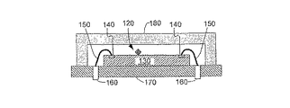
図1は、半導体のダイ(チップ)130の上に形成された、そのような構造体120の一例を示している。ダイ130は、電気回路(図示せず)や、構造体120とコンタクトパッド140とを接続する相互接続線を有している。ダイ130は、半導体ウエハ上に、他の複数のダイと同時にバッチ処理により製造される。ダイシングにより、ウエハからダイを分割(切り出した)後、ボンドワイヤ150により、コンタクトパッド140とリードフレームピン160とを接続する。そして、リードフレームは、ピン160が基板170の裏面から突出した状態で、セラミックの基板170内に封入される。ダイ130と構造体120とを保護するために、別の基板180が、基板170に接合されている。なお、構造体120が光学デバイス(例えば、ミラーや、光学センサー)の場合は、基板180は例えばガラスなどの適切な透明材料から作られる。
【0004】
前記したようなデバイスに適した製造技術及び構造体の改善が望まれる。また、非電子的に機能する部品の有無を問わず、デバイスの機械的強度を向上させることが望まれる。
【発明の開示】
【発明の概要】
【0005】
本発明のいくつかの実施形態は、微小電気機械及び微小電気光学構造体の技術と、垂直統合に用いられるPCT番号WO 98/19337(TruSi Technologies,LLC, May 7,1998)に記載されている裏面側接触の作成技術を結びつけるものである。
【0006】
本発明は、これらの実施形態に限定されるものではない。ある実施形態では、製造方法は、1つ又は複数の基板を備えた構造体を形成する過程を有し、前記1つ又は複数の基板は、単一の基板又は複数の基板を互いに結合したものからなり、前記構造体は、前記1つ又は複数の基板の少なくとも一部を含む、及び/又は前記1つ又は複数の基板に取り付けられた非電子機能部品を有し、前記1つ又は複数の基板は、第1面、前記第1面側に設けられた開口、開口内に設けられた導体を備える第1の基板を含み、当該方法が更に、前記第1の基板における第2面において前記導体が露出するように、前記構造体から材料を除去する過程を含むことを特徴とする。
【0007】
また、ある実施形態では、前記第2面は、前記第1の基板の裏側であり、露出された導体がコンタクトパットとなる。前記第1の基板の表面は、その他の基板、又は結合工程中(導体を露出させる工程を含む)に前記非電子機能部品を保護する基板と結合される。前記非電子機能部品は、ダイシング中も保護される。
【0008】
前記他の基板又は基板は、光学部品の場合は、必用に応じて透明にすることができる。その場合、前記他の基板は又は基板は、光学ひずみを減少させるために、前記非電子機能部品の近くに位置することが望ましい。また、このことにより、システムエリアを小型化することができる。
【0009】
また、ある実施形態では、製造方法は、第1面、前記第1面に設けられた開口、前記開口内に設けられた導体を含む第1の基板を有する構造体を製造した後、前記第1の基板における第2面において前記導体を露出させるために材料を除去する。このとき、前記第1の基板の前記第2面における第1部分から材料を除去することにより、前記第1部分を前記第1の基板の前記第2面における第1部分よりも凹設する。
【0010】
作成された構造体は、非電子機能部品を有していてもよいし、有していなくともよい。ある実施形態では、前記第1の基板は、前記第2部分において、前記第1部分よりも厚い。前記第2部分を厚くすることにより、前記構造体の機械強度を向上させることができる。
【0011】
本発明の他の特徴及び利点は、以下に説明する。
【発明を実施するための最良の形態】
【0012】
図2−Aは、ウエハ210上及び/又は内部に作成された、小型の構造体120を示す。構造体120は、光学的、機械的、磁気的、及び/又はその他の種類の非電子的に機能する部品(非電子機能部品)を含む。非電子機能部品は、電子回路(例えばトランジスタ)を備えていてもよいし、備えていなくてもよい。だが、非電子機能部品の動作は、従来の電子回路には無い機能を有している。例えば、非電子機能部品は、動作中に、動く又は変形する必要がある。このような非電子機能部品の例としては、マイクロポンプのダイアフラムや、微小機械スイッチの作動部分がある。
【0013】
また、非電子機能部品には、可視又は不可視の光(電磁放射線)を放射及び/又は検出するものもある。「J. E. Gulliksen, "MST vs. MEMS: WHERE ARE WE ", Semiconductor Magazine, Oct. 2000, Vol. 1, No. 10」を参照されたい。このような非電子機能部品としては、ミラーやレンズがある。このような非電子機能部品は、指紋認識装置、光ディスクリーダ、バーコードリーダ、その他の微小機械システム(MEMS)やMST構造体内に設けられているものであってよい。
【0014】
また、非電子機能部品には、外部の磁場に対して、互いに作用し合うものもある。なお、本発明は、特定の種類の部品に限定されるものではない。また、本発明は、既存の部品以外に適用することも可能である。
【0015】
構造体120の非電子機能部品には、基板210の一部を含むものもある。また、非電子機能部品には、他の基板(図示しない)上で作成された後、その基板から切り離された部品を含むものもある。例えば、米国特許第6,076,256号(released mirrors)を参照されたい。
【0016】
構造体120は、基板210上及び/又は内部に作成された回路220に接続されている。回路220は、非電子機能部品の動作のために使用される。この回路220は、非電子機能部品をコントロールする、又は非電子機能部品の状態を示す信号を受信する。このような回路220としては、アンプ、フイルタ、又はその他の電子回路がある。基板210は、例えばシリコンなどの、適宜な半導体材料から作成することができる。また、ある実施形態では、回路220は接続線のみからなる。これらの実施形態では、基板210は、例えば誘電性ポリマやガラスなどの半導体以外の材料から作成される場合もある。
【0017】
回路220及び/又は構造体120は、接続用構造体230に接続されている。接続構造体230の一つを、図2−Bに拡大して示す。接続構造体230は、例えば、PCT番号第WO 98/19337号(Tru Si Technologies, LLC, May 7, 1998)、2001年2月6日出願の米国特許出願第6,184,060号、2001年11月27日出願の米国特許出願第6,322,903号に記載されている方法により作成することができる。これらの方法は、言及することをもって、本願明細書の一部とする。
【0018】
接続構造体230の作成方法について簡単に説明すると、バイア260は、基板210内にエッチングされる。絶縁体270は、バイア260内に形成される。導体280(例えば金属)は、絶縁体270上に形成される。また、所望に応じて、バイア260を充填するために、導体280上に他の材料290を形成することもできる。
【0019】
なお、ウエハ210が絶縁性材料から作成される場合は、絶縁体270を省略することができる。また、バイア260を導体280によって充填することもできる。
【0020】
構造体120、回路220、及び接続構造体230は、どの順序で作成してもよい。例えば、最初に回路220を作成し、次に接続構造体230を作成し、最後に構造体120を作成することもできる。また、要素230、220、120を作成するステップは、交互に行うことができる。そして、これらの要素の一つ以上を作成するのに同じステップを用いることができる。
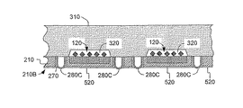
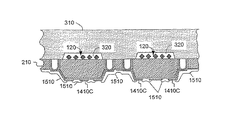
【0021】
図3は、ウエハ210に結合されるウエハ310を示す。ウエハ310には、複数のキャビティ320が形成されている。基板310には、キャビティ320と同じ側又は反対側に、位置合わせ用の印(図示しない)を形成することができる。ある実施形態では、ウエハ310は、上面及び下面に、ガラス磨きがされている。また、ある実施形態では、ウエハ310とウエハ210は、両者の熱膨張率を一致させるため、同一種類の材料(例えばシリコン)から作成される。
【0022】
キャビティ320と、位置合わせ用の印は、従来の方法により形成することができる。例えば、米国特許番号第6,097,140号(glass etch)を参照されたい。
【0023】
ウエハ310,210は互いに結合される(図4参照)。このとき、構造体120は、キャビティ320内に位置する。ウエハ310,210は、例えば接着剤や真空中でのガラス・フリットなどの、従来の方法により結合させることができる。また、接着剤を塗布する前や、構造体120がウエハ210に取り付けられる前に、ウエハ210を接着剤から隔離するために、ウエハ210の一部を隔離用の材料により覆うこともできる。
【0024】
また、ウエハ310,210は、ハンダ付け、共晶接合、エポキシ樹脂による熱圧着、その他の公知又はこれから発明されるであろう方法によっても結合させることができる。
【0025】
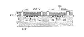
そして、ウエハ210の下面210B(ウエハ310に結合される側の反対側)は、バイア260の底部に形成された導体280からなる接続部280Cが露出するように処理される。この処理は、米国特許出願第6,322,903号や、PCT番号第WO 98/19337号に記載されている方法により行うことができる。そのような方法の一つによれば、基板210と絶縁体270は、接続部280Cを露出させるために、常圧プラズマエッチング法によりエッチングされる。そして、絶縁層520(図6参照)は、シリコン210上に、導体280上を避けて選択的に形成される。
【0026】
他の方法では、基板210と絶縁体280をエッチングして、導体280を露出させた後に、基板210を逆さまにする(図7参照)。そして、絶縁層520がスピンオン又はスプレー工程により形成された後、硬化される。絶縁層520としては、ポリイミド、ガラス、その他の流動性を有する材料(例えば、流動性熱硬化性重合体)を用いることができる。層520の表面は略平面状に形成されており、少なくとも、接続構造体230上では、層520は他の部分よりも薄く形成されている。
【0027】
ある実施形態では、層520は、接続部280Cを覆ってはいない。絶縁層520が接続部280Cを覆っている場合は、必要ならば、接続部280Cを十分に露出させるために、層520をブランケットエッチング法によりエッチングすればよい。ウエハ基板210の結果は、図5に示すようになる。
【0028】
また、他の方法では、構造体210のエッチングは、導体280ではなく絶縁体270を露出させる。図8を参照して、絶縁体270は、基板210の表面から突出している。ウエハ基板210は、逆さまにされており(図8参照)、絶縁層520は、前記した図7のような方法で形成される。層520は、接続構造体230上では、他の部分よりも薄い。
【0029】
ある実施形態では、層520は、接続部280Cを覆ってはいない。また、必要ならば、絶縁体270を十分に露出させるために、層520をブランケットエッチング法によりエッチングすればよい(図9参照)。そして、導体280を露出させるために、絶縁体270は、絶縁層520から選択的にエッチングされる。ある実施形態では、絶縁体270は二酸化珪素からなり、絶縁層520はポリイミドからなる。ウエハ基板210の結果は、図6に示すようになる。
【0030】
図5〜9に示した処理における利点の一つとしては、リソグラフィを行う必要がない。なお、リソグラフィを含む技術に含まれる他の技術も同様に使用することができる。
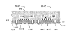
【0031】
ウエハ基板210は、個々のチップ1010にダイシングされる(図10参照)。ダイシング中は、構造体210は、基板210,310により保護される。
【0032】
チップ1010は、例えばプリント基板(PCB)などの配線用基板(図示せず)に取り付けられる。接続部280Cは、フリップ・チップ技術を用いて、配線用基板に直接取り付けられる。前記した米国特許出願第6,322,903号を参照されたい。
【0033】
また、チップ1010は、接続部280Cが上を向くように、逆さまにされた後、リードフレームにワイヤボンディングされ、そして、従来の方法により、パッケージされることもできる。ボールグリッドアレイ(Ball grid arrays)、チップスケールパッケージ(chip scale packages)、その他の公知又はこれから発明されるであろうパッケージ技術を用いることができる。
【0034】
また、他の有利な点としては、ウエハ210,310を結合した後、基板210と回路220を両ウエハにより保護することができる。基板310は、図1のように、基板210の周りに広がっていないので、基板210と回路220を保護する空間は小さくて済む。基板310が構造体120の近くに位置するように、キャビティ320は浅く形成されることが好ましい。このようにすると、光学的ひずみを減少させることができるので、光学的な用途に用いる場合に好適である。さらに、基板310は基板210上に直接載置されるので、基板120に対して基板310を正確に位置決めすることが容易となる。
【0035】
光学的な用途に用いる場合は、基板310は非反射コーティングによって覆うことが好ましい。また、キャビティ320には、適宜な屈折率の材料が充填されることが好ましい。基板310には、レンズをエッチングすることができる。
【0036】
基板310は、構造体120及び/又は回路220と接続される電子回路を有していてもよい。基板310は、絶縁体や半導体材料から作成してもよい。米国特許出願第6,322,903号には、基板310の回路を回路220に接続するために用いられる技術が記載されている。
【0037】
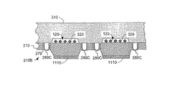
図11は、エリアに適合したパッケージを得るために、ウエハ210の裏側210Bに沿って、裏側の接続部が再配分された実施形態を示す。図4の工程の後、マスク1110が基板210の裏側210Bに形成され、リソグラフィによってパターンが形成される。所望に応じて、マスクが形成される前に、基板210は裏側210Bから薄くすることができる。ただし、このとき、絶縁体270を露出させる必要はない。薄くすることは、機械的研磨、プラズマエッチング、その他の公知又はこれから発明されるであろう方法により行うことができる。
【0038】
裏側210B上の導体280の接続部280Cを露出させるため、基板210と絶縁体270は、マスク1110から選択的にエッチングされる(図12参照)。適宜なエッチング処理は、前記した図5のような方法で行われる。そして、マスク1110が取り除かれた後、基板120の裏側210Bにおける導体280上以外に、絶縁層520(図13参照)が選択的に形成される。前記した図6のような方法を参照されたい。
【0039】
導電層1410(図14参照)、例えば集積回路を結合したパッドに適宜な金属は、導電パッド1410Cと、それらのパッドを導体280に接続する導電線とを形成するために、ウエハ210の裏側に形成されパターンされる。そして、適宜な絶縁層1510(図15参照)は、導電パッド1410Cを露出させるために形成されパターンされる。
【0040】
そして、ウエハ基板120はダイシングされる(図16参照)。結果として得られるチップ1010のパッド1410Cは、例えばPCBなどの配線用基板に直接取り付けられる。一つのチップ1010の底面図を図17に示す。また、図17は、図11に示したマスク1110の輪郭も示している。
【0041】
図11〜17に示した実施形態における利点は、下記の点である。
【0042】
接続構造体230の位置が、回路220と基板120との配置により規制される。例えば、接続構造体230は、チップ1010の表面において規制される。
【0043】
また、接続部280Cが、配線用基板に直接取り付けられないので、そのサイズを小型化することができる。
【0044】
また、導電パッド1410Cのサイズは、配線用基板に直接取り付けられるだけ十分に大きいが、導電パッド1410Cの位置は回路220や基板120により規制されない。そのため、チップ面積をより小型化することができる。
【0045】
図18では、マスク1110は、その境界(例えば隅部)において、4つの延出部(extensions)1110Eを有している。これらの延出部1110Eは、チップ1010の機械的強度を高める。延出部1110Eは、接続部280Cの境界の近く、又はすぐ近くに位置してもよい。ある実施形態では、延出部は、チップの境界に達し、隣接するチップの延出部と結合している。また、延出部は、接続部280間に延びていてもよい。なお、延出部は、4つ以上又は4つ以下設けることもできる。
【0046】
また、延出部は、非電子機能部品を有しない基板に形成することもできる。
【0047】
他の実施形態では、ウエハ基板210は、前記した図5〜9のどの方法によっても、図6の工程まで処理される。そして、コンタクトパッド1410Cと、コンタクトパッド1410Cを導体280に接続するための導電線とを形成するために、導電層1410(図19参照)が、前記した図14の方法により、ウエハ210の裏側210Bの絶縁層520上に、形成され、パターンされる。このとき、マスクは使用しない。そして、コンタクトパッド1410Cを露出させるために、前記した図15の方法により、絶縁層1510が形成され、パターンされる。
【0048】
そして、ウエハ基板は、テストされた後、個々のチップ1010を作成するためにダイシングされる(図20参照)。
【0049】
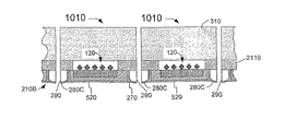
図21は、ウエハ310の他の処理方法を示している。ウエハ310には、キャビティがエッチングされていない。離隔部材(stand-off features)2110は、ウエハ310の下面に形成されている。離隔部材2110は、適宜な材料を積層させて、その材料をリソグラフィによりパターンングすることや、シルクスクリーン印刷や、材料を針により処理することや、その他の公知又はこれから発明されるであろう方法により形成することができる。適宜な材料としては、エポキシ樹脂や、熱硬化性重合体や、ガラス・フリットなどがある。
【0050】
ウエハ210は、図3のように処理される。そして、ウエハ310,210は、位置合わせがなされた後、図22のように結合される。このとき、離隔部材2110は、ウエハ210に結合される。ウエハ210,310が結合された際は、構造体120は、離隔部材2110,2110間に位置する。そして、ウエハ基板は、前記した図5〜20のどの方法によっても処理される。
【0051】
図22に示す実施形態では、材料2110は、バイア260を充填するのに使用される。この場合、図22では、図2−Bにおいてバイア260を充填するのに使用された材料290は存在しない。或いは、材料290は、バイア260を部分的に充填するのにしか使用されない。材料2110は、ウエハ210,310が結合されたときは、完全には固まらない。材料2110は、ウエハ210,310の結合中、バイア260を充填する。ウエハ210,310の結合は、バイア260に材料2110を充填するのを容易にするために、真空中で行われる。
【0052】
材料2110が固まる前にウエハ210,310の結合が始まる場合は、ウエハ310とウエハ210間における構造体210損傷を防止するために必用な最小限の間隔を保つために、ウエハ310及び/又はウエハ210上には、スペーサが設けられる。
【0053】
スペーサとしては、ウエハ上に固定された硬い部材を用いることができる。また、スペーサとしては、材料2110内に埋め込まれた硬い球状部材2120(図22参照)を用いることもできる。球状部材は、ガラス、樹脂、その他の適宜な材料(できれば導電体)から作成することができる。
【0054】
球状部材2120は、ウエハ310,210が結合された際に、ウエハ310,210間の最小限の間隔を保つ。球状部材の好ましい直径は、10〜30μmである。なお、球状部材の直径は、ウエハ310,210間の保つべき間隔に基づいて決定される。2000年7月25日に交付された米国特許番号第6,094,244号を参照されたい。
【0055】
ある実施形態では、離隔部材2110が構造体120を完全に取り囲み、構造体120が位置する範囲を真空に保っている。真空にすることにより、構造体120の周囲の気圧が大気圧まで高まったときに、構造体120を密閉して周囲から隔離するのに役立つ。また、真空にすることにより、ウエハ310,210間の結合の強度も向上する。
【0056】
ある実施形態では、材料2110は、ウエハ310上ではなく、ウエハ210上に形成される。
【0057】
また、ある実施形態では、材料2110は、構造体120を覆う、かつ接触する。
【0058】
また、ある実施形態では、材料2110は、ウエハ310,210が結合される前に固められる。この場合、材料2110は、バイア260を充填するのには使用されない。
【0059】
図23に示す実施形態では、構造体120は基板120の表面から突出していない。また、ウエハ310には、キャビティや離間部材は設けられていない。このことにより、基板310と構造体120間の間隔を狭くすることができる。これは、構造体120が光学部品を有している場合は、特に利点となる。
【0060】
図24〜26に示す実施形態では、少なくとも接続構造体230のいくつかがチップ同士の境界(ダイシングライン上)に配置されている。その他の点では、ウエハ310,210の処理は、前記した図5〜23のどの方法によっても続行することができる。図24は、図4のように加工されたウエハ基板を示している。また、図25は、ダイシングされた後の基板を示している。また、図26は作成されたチップ1010の底面図である。
【0061】
接続構造体230をチップ同士の境界に配置することの利点の一つは、面積を減らすことができるということである。また、特に、材料290が導電性の場合や、材料290が省略されている場合は、接続構造体230が、チップの側面に接触することができるという利点もある。また、もし、ウエハ基板210が図16や図20のように処理された場合は、接続構造体230が側面において接続している間は、接続部140Cはウエハ基板210の裏側で使用可能である。
【0062】
また、図24に示すように、バイア260の幅を広く形成することにより、バイアを等方性エッチング(isotropic etching)により形成することが可能になる。なお、等方性エッチングは、異方性エッチング(anisotropic etching)よりも安上がりである。
【0063】
また、バイア260は、図22のように、材料2110で充填することもできる。
【0064】
なお、図24〜26に示す実施形態では、ウエハ310は図21のように処理されている。また、接続構造体230がチップの境界に配置されている場合の他の実施形態では、ウエハ310は、図3や図23のように処理されている。
【0065】
図27に示す実施形態では、キャビティ2710が、ウエハ310の上面に、ダイシングラインに沿って形成されている。キャビティ2710は、ウエハ310,210の結合前でも結合後でも形成することができる。また、キャビティ2710は、ダイシングラインの全長に、又はダイシングラインに沿って分散して、どのような形状でも形成することができる。
【0066】
図28は、ダイシング後の基板を示している。キャビティ2710は、ダイシング中に、基板にかかる圧力や、基板に圧力がかかる時間を減少させる。そのため、ダイシングによる損傷は少なくなる。このことは、基板310が光学的な目的に用いられる透明な基板である場合には、特に有利である。なぜならば、基板310の損傷は、光学的ひずみの原因となるからである。
【0067】
キャビティ2710は、前記した図2〜26の基板や処理において、どれにでも適用することができる。
【0068】
基板290は、多層ウエハ(multiple wafers)を用いて作成することができる。図29に示す例では、構造体120は、ウエハ210と、ウエハ210の上面側に結合された複数のウエハ2904との一部分を含んでいる。このような構造体120としては、例えばマイクロポンプがある。例として、2000年11月12日に交付された米国特許番号第6,116,863号の「Electromagnetically Driven Microactuated Device and Method of Making the Same」を参照されたい。図29では、ウエハ310に形成された通路2910が、マイクロポンプにおける出入口に相当する。
【0069】
作成中は、ウエハ2904と、ウエハ210の上面側は、構造体120が作成できるように処理される。そして、ウエハ210,ウエハ2904は結合される。また、ウエハ310は、必要に応じて、例えば、図3のようなキャビティ320や、図24のような離隔部材2110を形成できるように処理される。そして、ウエハ310は、ウエハ2904の上面に結合される。その後、前記した図4〜28のような作成工程が続けられる。ウエハ210の下側は接続構造体230を露出させるように処理される。図29に示したウエハ210の裏側は、図19のように処理される。ただし、前記した他の処理でもよい。図29は、ダイシングされた後の 構造を示している。
【0070】
前記した実施形態は、本発明を限定するものではない。また、本発明は、特定の材料、処理、形状、配置、構造体120の特定の種類によって限定されるものではない。また、構造体120は、動作中に動く機械部品を有していてもよい。また、他の実施形態や変形例は、〔特許請求の範囲〕において規定された範囲に含まれる。
【図面の簡単な説明】
【0071】
【図1】従来の微小電子機械部品又は微小電子光学構造体を有するデバイスを示す縦断面図である。
【図2−A】本発明の一実施形態に係る非電子機能部品を有するデバイスを示す縦断面図である。
【図2−B】図2−Aに示した接続構造体230の拡大図である。
【図3】図2−Aに示したウエハ210に結合されるウエハ310を示す縦断面図である。
【図4】デバイスの製造工程を示す図であり、ウエハ210,310を結合させた状態を示す。
【図5】図4に続く工程であり、ウエハ210の下面210Bを処理した状態を示す。
【図6】図5に続く工程であり、ウエハ210の下面210Bに絶縁層520を形成した状態を示す。
【図7】デバイスの他の製造方法を示す図であり、ウエハ310に逆さまにした基板210を結合させた状態を示す。
【図8】図7に続く工程であり、絶縁体270を露出させた状態を示す。
【図9】図8に続く工程であり、絶縁層520を形成した状態を示す。
【図10】図6に続く工程であり、基板210,310をダイシングした状態を示す。
【図11】デバイスの他の製造方法を示す図であり、図4の工程の後、基板210の裏側210Bにマスク1110を形成した状態を示す。
【図12】図11に続く工程であり、導体280の接続部280Cを露出させた状態を示す。
【図13】図12に続く工程であり、絶縁層520を形成した状態を示す。
【図14】図13に続く工程であり、導電層1410を形成した状態を示す。
【図15】図14に続く工程であり、絶縁層1510を形成した状態を示す。
【図16】図15に続く工程であり、基板210,310をダイシングした状態を示す。
【図17】図15の工程で作成されたチップ1010の底面図である。
【図18】図15の工程で作成されたチップ1010の底面図であり、チップ1010が延出部1110Eを有している場合を示す。
【図19】デバイスの他の製造方法を示す図であり、図6の工程の後、絶縁層520上に導電層1410を形成した状態を示す。
【図20】図19に続く工程であり、基板210,310をダイシングした状態を示す。
【図21】ウエハ310の他の処理方法を示す図であり、ウエハ310の下面に離隔部材2110を形成した状態を示す。
【図22】図21に続く工程であり、ウエハ210,310を結合させた状態を示す。
【図23】デバイスの他の製造方法を示す図であり、構造体120がウエハ120内に配置されている様子を示す。
【図24】デバイスの他の製造方法を示す図であり、接続構造体230をダイシングライン上に配置されている様子を示す。
【図25】図24に続く工程であり、基板210,310をダイシングした状態を示す。
【図26】図25の工程で作成されたチップ1010の底面図である。
【図27】デバイスの他の製造方法を示す図であり、ウエハ310の上面にキャビティ2710を形成した状態を示す。
【図28】図27に続く工程であり、基板210,310をダイシングした状態を示す。
【図29】デバイスの他の製造方法を示す図であり、複合ウエハを用いて作成したチップ1010を示す。【Technical field】
[0001]
TECHNICAL FIELD The present invention relates to a device having an opening penetrating a substrate and having a conductor provided in the opening. The invention also relates to a method for manufacturing the device. Devices according to the invention include components that function non-electronically. Examples of such devices include micro-electro-mechanical systems (MEMS) and other micro-structure-technology (MST) structures.
[Background Art]
[0002]
Integrated circuit manufacturing techniques have been used to create micro-electro-mechanical structures and micro-electro-optical structures. Examples of such structures include relays, micropumps, optical devices for fingerprint verification, and the like.
[0003]
FIG. 1 shows an example of such a
[0004]
Improvements in manufacturing techniques and structures suitable for such devices are desired. It is also desirable to improve the mechanical strength of the device, regardless of the presence or absence of non-electronically functioning components.
DISCLOSURE OF THE INVENTION
Summary of the Invention
[0005]
Some embodiments of the present invention are described in PCT No. WO 98/19337 (TruSi Technologies, LLC, May 7, 1998) used for micro-electro-mechanical and micro-electro-optical structure technology and vertical integration. This is to combine the technology for creating backside contacts.
[0006]
The present invention is not limited to these embodiments. In certain embodiments, the method includes forming a structure comprising one or more substrates, the one or more substrates comprising a single substrate or a plurality of substrates bonded together. Wherein said structure comprises at least a portion of said one or more substrates and / or has non-electronic functional components attached to said one or more substrates, and wherein said one or more The substrate includes a first substrate having a first surface, an opening provided on the first surface side, and a conductor provided in the opening, the method further comprising: providing the first substrate with a second surface on the second surface of the first substrate. Removing the material from the structure so that the conductor is exposed.
[0007]
In one embodiment, the second surface is a back side of the first substrate, and the exposed conductor serves as a contact pad. The surface of the first substrate is bonded to another substrate or a substrate that protects the non-electronic functional component during a bonding step (including a step of exposing a conductor). The non-electronic functional component is protected during dicing.
[0008]
In the case of an optical component, the other substrate or the substrate can be made transparent as necessary. In that case, it is desirable that the other substrate or the substrate is located near the non-electronic functional component in order to reduce optical distortion. In addition, this makes it possible to reduce the size of the system area.
[0009]
In one embodiment, the manufacturing method includes manufacturing a structure having a first substrate including a first surface, an opening provided in the first surface, and a conductor provided in the opening. The material is removed to expose the conductor on the second surface of the one substrate. At this time, by removing material from the first portion on the second surface of the first substrate, the first portion is recessed from the first portion on the second surface of the first substrate.
[0010]
The created structure may or may not have a non-electronic functional component. In one embodiment, the first substrate is thicker in the second portion than in the first portion. By increasing the thickness of the second portion, the mechanical strength of the structure can be improved.
[0011]
Other features and advantages of the invention are described below.
BEST MODE FOR CARRYING OUT THE INVENTION
[0012]
FIG. 2-A shows a
[0013]
Some non-electronic functional components emit and / or detect visible or invisible light (electromagnetic radiation). See "JE Gulliksen," MST vs. MEMS: WHERE ARE WE ", Semiconductor Magazine, Oct. 2000, Vol. 1, No. 10. Such non-electronic functional parts include mirrors and lenses. Such non-electronic functional components may be provided in a fingerprint recognition device, an optical disk reader, a bar code reader, other micro mechanical systems (MEMS) or an MST structure.
[0014]
Some non-electronic functional components interact with each other against an external magnetic field. The invention is not limited to a particular type of component. Further, the present invention can be applied to components other than existing components.
[0015]
Some non-electronic functional components of the
[0016]
The
[0017]
The
[0018]
Briefly describing the method of making the
[0019]
When the
[0020]
The
[0021]
FIG. 3 shows
[0022]
The
[0023]
[0024]
The
[0025]
Then,
[0026]
In another method, the
[0027]
In some embodiments,
[0028]
In another method, the etching of the
[0029]
In some embodiments,
[0030]
One of the advantages of the processing shown in FIGS. 5-9 is that lithography need not be performed. Note that other technologies included in the technology including lithography can be used as well.
[0031]
The
[0032]
The
[0033]
Alternatively, the
[0034]
Another advantage is that after bonding the
[0035]
For optical applications, the
[0036]
The
[0037]
FIG. 11 shows an embodiment in which the backside connections have been redistributed along the
[0038]
[0039]
A metal suitable for the conductive layer 1410 (see FIG. 14), for example, the pads to which the integrated circuits are bonded, is formed on the back side of the
[0040]
Then, the
[0041]
The advantages of the embodiment shown in FIGS. 11 to 17 are as follows.
[0042]
The position of the
[0043]
In addition, since the
[0044]
The size of the
[0045]
In FIG. 18, the
[0046]
Further, the extension portion can be formed on a substrate having no non-electronic functional component.
[0047]
In another embodiment, the
[0048]
Then, after being tested, the wafer substrate is diced to create individual chips 1010 (see FIG. 20).
[0049]
FIG. 21 shows another processing method of the
[0050]
The
[0051]
In the embodiment shown in FIG. 22,
[0052]
If the bonding of the
[0053]
A hard member fixed on the wafer can be used as the spacer. Further, a hard spherical member 2120 (see FIG. 22) embedded in a
[0054]
The
[0055]
In some embodiments, the
[0056]
In some embodiments,
[0057]
Also, in some embodiments,
[0058]
Also, in some embodiments, the
[0059]
In the embodiment shown in FIG. 23, the
[0060]
In the embodiment shown in FIGS. 24 to 26, at least some of the
[0061]
One of the advantages of arranging the
[0062]
Also, as shown in FIG. 24, forming the width of the via 260 wide allows the via to be formed by isotropic etching. It should be noted that isotropic etching is cheaper than anisotropic etching.
[0063]
The via 260 can also be filled with a
[0064]
In the embodiment shown in FIGS. 24 to 26, the
[0065]
In the embodiment shown in FIG. 27, the
[0066]
FIG. 28 shows the substrate after dicing. The
[0067]
The
[0068]
[0069]
During fabrication, the
[0070]
The embodiments described above do not limit the present invention. Also, the invention is not limited by a particular material, process, shape, arrangement, or particular type of
[Brief description of the drawings]
[0071]
FIG. 1 is a longitudinal sectional view showing a device having a conventional microelectromechanical component or microelectronic optical structure.
FIG. 2A is a longitudinal sectional view showing a device having a non-electronic functional component according to one embodiment of the present invention.
FIG. 2-B is an enlarged view of the
FIG. 3 is a longitudinal sectional view showing a
FIG. 4 is a diagram showing a device manufacturing process, showing a state where
FIG. 5 is a process subsequent to FIG. 4 and shows a state where the
FIG. 6 is a process subsequent to FIG. 5 and shows a state in which an insulating
FIG. 7 is a view showing another method of manufacturing the device, and shows a state in which an
FIG. 8 is a step subsequent to FIG. 7 and shows a state in which an
FIG. 9 is a step subsequent to FIG. 8 and shows a state in which an insulating
FIG. 10 is a process subsequent to FIG. 6, and shows a state where the
11 is a view showing another method of manufacturing the device, and shows a state where a
FIG. 12 is a process subsequent to FIG. 11 and shows a state in which a
FIG. 13 is a process subsequent to FIG. 12 and shows a state where an insulating
FIG. 14 is a step subsequent to FIG. 13 and shows a state where a
FIG. 15 is a step subsequent to FIG. 14 and shows a state in which an insulating
FIG. 16 is a process subsequent to FIG. 15 and shows a state where the
FIG. 17 is a bottom view of the
FIG. 18 is a bottom view of the
19 is a view illustrating another method of manufacturing the device, and shows a state where a
FIG. 20 is a process subsequent to FIG. 19 and shows a state where the
21 is a view showing another processing method of the
FIG. 22 is a process subsequent to FIG. 21 and shows a state where the
FIG. 23 is a diagram illustrating another method of manufacturing the device, and illustrates a state where the
FIG. 24 is a view showing another method of manufacturing the device, and shows a state where the
FIG. 25 is a process subsequent to FIG. 24 and shows a state where the
FIG. 26 is a bottom view of the
FIG. 27 is a diagram illustrating another method of manufacturing the device, and shows a state where a
FIG. 28 is a process subsequent to FIG. 27 and shows a state where the
FIG. 29 is a diagram illustrating another method of manufacturing the device, and illustrates a
Claims (57)
前記1つ又は複数の基板は、単一の基板又は複数の基板を互いに結合したものからなり、
前記構造体は、前記1つ又は複数の基板の少なくとも一部を含む、及び/又は前記1つ又は複数の基板に取り付けられた非電子機能部品を有し、
前記1つ又は複数の基板は、第1面、前記第1面側に設けられた開口、開口内に設けられた導体を備える第1の基板を含み、
当該方法が更に、前記第1の基板における第2面において前記導体が露出するように、前記構造体から材料を除去する過程を含むことを特徴とする製造方法。Forming a structure comprising one or more substrates,
The one or more substrates comprise a single substrate or a plurality of substrates joined together;
The structure includes at least a portion of the one or more substrates and / or has non-electronic functional components attached to the one or more substrates;
The one or more substrates include a first substrate having a first surface, an opening provided on the first surface side, and a conductor provided in the opening.
The method of claim 1, further comprising removing material from the structure such that the conductor is exposed on a second surface of the first substrate.
前記複数の基板の一つをなす基板S1上に、周囲よりも突出した離隔部材を設ける過程と、
前記離隔部材が、前記基板S1と、前記複数の基板の一つをなす別の基板S2との間に位置するように、前記基板を互いに結合する過程とを有し、
前記第1の基板が、前記両基板S1、S2の一方からなることを特徴とする請求項3に記載の製造方法。The structure forming process,
Providing a separating member protruding from the surroundings on a substrate S1 which constitutes one of the plurality of substrates;
Bonding the substrates to each other so that the separation member is located between the substrate S1 and another substrate S2 forming one of the plurality of substrates.
4. The method according to claim 3, wherein the first substrate is formed of one of the two substrates S1 and S2.
前記1つ又は複数の基板は、単一の基板又は複数の基板を互いに結合したものからなり、
前記1つ又は複数の基板は、第1面、第2面、前記第1面から前記第2面に貫通する開口、及び前記開口内に設けられた導体を含み、
前記導体は前記第2面側に露出し、
前記構造体は、前記第1の基板側における前記第1面の少なくとも一部を含む、及び/又は前記第1の基板における前記第1面に取り付けられた非電子機能部品を有することを特徴とするデバイス。A device having a structure with one or more substrates, comprising:
The one or more substrates comprise a single substrate or a plurality of substrates joined together;
The one or more substrates include a first surface, a second surface, an opening penetrating from the first surface to the second surface, and a conductor provided in the opening,
The conductor is exposed on the second surface side,
The structure includes at least a part of the first surface on the first substrate side and / or has a non-electronic functional component attached to the first surface on the first substrate. Device to do.
前記第1の基板が、前記両基板S1、S2の一方からなることを特徴とする請求項20に記載のデバイス。The structure has a separating member between the substrate S1 and the substrate S2 that form the one or more substrates,
The device according to claim 20, wherein the first substrate comprises one of the two substrates S1, S2.
前記第1の基板における前記第2面において前記導体を露出させるために前記基板から材料を除去し、
前記第1の基板における前記第2面の第1部分から材料を除去することにより、前記第1の部分を前記第1の基板における前記第2面の第2部分に対して凹設することを特徴とする製造方法。Forming a structure having a first surface, an opening provided in the first surface, and a first substrate including a conductor provided in the opening;
Removing material from the substrate to expose the conductor on the second surface of the first substrate;
Removing the material from the first portion of the second surface of the first substrate so that the first portion is recessed with respect to the second portion of the second surface of the first substrate. Characteristic manufacturing method.
前記開口は前記チップの境界付近に位置し、前記第2部分は前記チップの境界に向かって延出する延出部を有していることを特徴とする請求項9又は請求項31に記載の製造方法。The structure constitutes a chip,
The said opening is located near the boundary of the said chip | tip, The said 2nd part has an extension part extended toward the boundary of the said chip | tip, The Claims 9 or 31 characterized by the above-mentioned. Production method.
前記延出部は、各開口間において前記境界に向かって延出することを特徴とする請求項32に記載の製造方法。The first substrate has a plurality of openings on the first surface side, a conductor is provided on each opening, and the second substrate is provided on each of the second openings by removing the material on the second surface side. Exposed conductor,
33. The method according to claim 32, wherein the extension portion extends toward the boundary between the openings.
前記第2面上に、前記第2部分において接続部を露出させた状態で、前記導体を覆う絶縁体を形成する過程とを含み、
前記接続部は前記1つ又は複数の相互接続線によって前記導体と電気的に接続することを特徴とする請求項9又は請求項31に記載の製造方法。Forming one or more interconnect lines on the second surface extending from the exposed conductor to the second portion;
Forming an insulator covering the conductor on the second surface in a state where the connection portion is exposed in the second portion,
32. The method according to claim 9, wherein the connection portion is electrically connected to the conductor by the one or more interconnection lines.
(A)前記第1の絶縁体を露出させるために、前記第2面から半導体材料を除去する過程と、
(B)前記導体を露出させるために、前記第2面上の前記第1の絶縁体を除去する過程とを含むことを特徴とする請求項14又は請求項40に記載の製造方法。The opening has a first insulator that isolates the conductor from a sidewall of the opening;
(A) removing semiconductor material from the second surface to expose the first insulator;
41. The method according to claim 14, further comprising the step of: (B) removing the first insulator on the second surface to expose the conductor.
前記半導体材料及び導体上に前記第2の絶縁体を形成する過程と、
前記半導体材料上の前記第2の絶縁体を完全に除去することなく、少なくとも前記導体の一部を覆う前記第2の絶縁体を完全に除去するため、前記第2の絶縁体をブランケットエッチング法によりエッチングする過程とを含むことを特徴とする請求項42に記載の製造方法。The step of forming the second insulator includes:
Forming the second insulator on the semiconductor material and the conductor;
Blanket etching the second insulator to completely remove the second insulator over at least a portion of the conductor without completely removing the second insulator on the semiconductor material 43. The method according to claim 42, further comprising the step of:
前記第1の基板は、第1面、第2面、前記第1面から前記第2面に貫通する開口、及び前記開口内に設けられ、前記第2面側に露出する導体を含み、
前記導体は、前記第2面における第1部分において露出し、
前記第2面は、該第2面から前記第1部分よりも突出している第2部分を有することを特徴とするデバイス。A device having a structure including a first substrate,
The first substrate includes a first surface, a second surface, an opening penetrating from the first surface to the second surface, and a conductor provided in the opening and exposed to the second surface side,
The conductor is exposed at a first portion of the second surface;
The device of claim 2, wherein the second surface has a second portion protruding from the second surface beyond the first portion.
前記第2面上で、前記第2部分において接続部を露出させた状態で、前記導体を覆う絶縁体とを有し、
前記接続部は前記1つ又は複数の相互接続線によって前記導体と電気的に接続することを特徴とする請求項47に記載のデバイス。One or more interconnect lines extending from the conductor exposed on the second surface to the second portion;
An insulator covering the conductor on the second surface in a state where the connection portion is exposed in the second portion;
48. The device of claim 47, wherein the connection is electrically connected to the conductor by the one or more interconnect lines.
Applications Claiming Priority (2)
| Application Number | Priority Date | Filing Date | Title |
|---|---|---|---|
| US09/791,977 US6717254B2 (en) | 2001-02-22 | 2001-02-22 | Devices having substrates with opening passing through the substrates and conductors in the openings, and methods of manufacture |
| PCT/US2002/005175 WO2002068320A2 (en) | 2001-02-22 | 2002-02-20 | Devices having substrates with openings passing through the substrates and conductors in the openings, and methods of manufacture |
Publications (2)
| Publication Number | Publication Date |
|---|---|
| JP2004525778A true JP2004525778A (en) | 2004-08-26 |
| JP2004525778A5 JP2004525778A5 (en) | 2005-06-02 |
Family
ID=25155420
Family Applications (1)
| Application Number | Title | Priority Date | Filing Date |
|---|---|---|---|
| JP2002567846A Pending JP2004525778A (en) | 2001-02-22 | 2002-02-20 | A device comprising a substrate having an opening therethrough and the method of manufacturing. |
Country Status (5)
| Country | Link |
|---|---|
| US (2) | US6717254B2 (en) |
| EP (1) | EP1412283A2 (en) |
| JP (1) | JP2004525778A (en) |
| AU (1) | AU2002306557A1 (en) |
| WO (1) | WO2002068320A2 (en) |
Cited By (2)
| Publication number | Priority date | Publication date | Assignee | Title |
|---|---|---|---|---|
| JP2007059769A (en) * | 2005-08-26 | 2007-03-08 | Honda Motor Co Ltd | Method of manufacturing semiconductor device, semiconductor device and wafer |
| JP2008538810A (en) * | 2005-03-03 | 2008-11-06 | キモンダ アクチエンゲゼルシャフト | Manufacturing method of thin layer structure |
Families Citing this family (92)
| Publication number | Priority date | Publication date | Assignee | Title |
|---|---|---|---|---|
| SG106050A1 (en) * | 2000-03-13 | 2004-09-30 | Megic Corp | Method of manufacture and identification of semiconductor chip marked for identification with internal marking indicia and protection thereof by non-black layer and device produced thereby |
| US6631935B1 (en) * | 2000-08-04 | 2003-10-14 | Tru-Si Technologies, Inc. | Detection and handling of semiconductor wafer and wafer-like objects |
| US20020117753A1 (en) * | 2001-02-23 | 2002-08-29 | Lee Michael G. | Three dimensional packaging |
| JP3788268B2 (en) * | 2001-05-14 | 2006-06-21 | ソニー株式会社 | Manufacturing method of semiconductor device |
| US6935830B2 (en) * | 2001-07-13 | 2005-08-30 | Tru-Si Technologies, Inc. | Alignment of semiconductor wafers and other articles |
| US6615113B2 (en) | 2001-07-13 | 2003-09-02 | Tru-Si Technologies, Inc. | Articles holders with sensors detecting a type of article held by the holder |
| CN1545484A (en) * | 2001-08-24 | 2004-11-10 | Ф�ء�����˹��˾ | Process for producing microelectromechanical components |
| US6856007B2 (en) * | 2001-08-28 | 2005-02-15 | Tessera, Inc. | High-frequency chip packages |
| US6787916B2 (en) * | 2001-09-13 | 2004-09-07 | Tru-Si Technologies, Inc. | Structures having a substrate with a cavity and having an integrated circuit bonded to a contact pad located in the cavity |
| WO2003054927A2 (en) * | 2001-11-07 | 2003-07-03 | The Board Of Trustees Of The University Of Arkansas | Structure and process for packaging rf mems and other devices |
| JP4110390B2 (en) * | 2002-03-19 | 2008-07-02 | セイコーエプソン株式会社 | Manufacturing method of semiconductor device |
| US6835589B2 (en) * | 2002-11-14 | 2004-12-28 | International Business Machines Corporation | Three-dimensional integrated CMOS-MEMS device and process for making the same |
| US6888233B2 (en) * | 2003-03-10 | 2005-05-03 | Honeywell International Inc. | Systems for buried electrical feedthroughs in a glass-silicon MEMS process |
| US6897148B2 (en) | 2003-04-09 | 2005-05-24 | Tru-Si Technologies, Inc. | Electroplating and electroless plating of conductive materials into openings, and structures obtained thereby |
| DE10331322A1 (en) * | 2003-07-10 | 2005-02-03 | Epcos Ag | Electronic component and method of manufacture |
| US20050067681A1 (en) * | 2003-09-26 | 2005-03-31 | Tessera, Inc. | Package having integral lens and wafer-scale fabrication method therefor |
| WO2005031861A1 (en) * | 2003-09-26 | 2005-04-07 | Tessera, Inc. | Structure and method of making capped chips including a flowable conductive medium |
| US20050116344A1 (en) * | 2003-10-29 | 2005-06-02 | Tessera, Inc. | Microelectronic element having trace formed after bond layer |
| DE10351028B4 (en) * | 2003-10-31 | 2005-09-08 | Infineon Technologies Ag | Semiconductor component and suitable manufacturing / assembly process |
| DE10356885B4 (en) * | 2003-12-03 | 2005-11-03 | Schott Ag | Method of housing components and housed component |
| DE10361521A1 (en) | 2003-12-03 | 2005-07-07 | Pac Tech - Packaging Technologies Gmbh | Method of alternate contacting of two wafers especially a semiconductor and a functional component wafer uses selected laser wavelength to fuse contact metallization only |
| EP1697966B1 (en) * | 2003-12-03 | 2013-02-13 | Pac Tech - Packaging Technologies GmbH | Method for the mutual contacting of two wafers |
| US20050139984A1 (en) * | 2003-12-19 | 2005-06-30 | Tessera, Inc. | Package element and packaged chip having severable electrically conductive ties |
| US20050189635A1 (en) * | 2004-03-01 | 2005-09-01 | Tessera, Inc. | Packaged acoustic and electromagnetic transducer chips |
| US7087134B2 (en) * | 2004-03-31 | 2006-08-08 | Hewlett-Packard Development Company, L.P. | System and method for direct-bonding of substrates |
| US7416984B2 (en) * | 2004-08-09 | 2008-08-26 | Analog Devices, Inc. | Method of producing a MEMS device |
| US7521363B2 (en) * | 2004-08-09 | 2009-04-21 | Analog Devices, Inc. | MEMS device with non-standard profile |
| US7288489B2 (en) * | 2004-08-20 | 2007-10-30 | Semitool, Inc. | Process for thinning a semiconductor workpiece |
| US20060040111A1 (en) * | 2004-08-20 | 2006-02-23 | Dolechek Kert L | Process chamber and system for thinning a semiconductor workpiece |
| US7193295B2 (en) * | 2004-08-20 | 2007-03-20 | Semitool, Inc. | Process and apparatus for thinning a semiconductor workpiece |
| US20060046499A1 (en) * | 2004-08-20 | 2006-03-02 | Dolechek Kert L | Apparatus for use in thinning a semiconductor workpiece |
| US7354649B2 (en) | 2004-08-20 | 2008-04-08 | Semitool, Inc. | Semiconductor workpiece |
| TWI245431B (en) * | 2004-09-10 | 2005-12-11 | Advanced Semiconductor Eng | Package structure and method for optoelectric products |
| US7300812B2 (en) | 2004-10-29 | 2007-11-27 | Hewlett-Packard Development Coompany, L.P. | Micro electrical mechanical system |
| US20060183270A1 (en) * | 2005-02-14 | 2006-08-17 | Tessera, Inc. | Tools and methods for forming conductive bumps on microelectronic elements |
| US8143095B2 (en) * | 2005-03-22 | 2012-03-27 | Tessera, Inc. | Sequential fabrication of vertical conductive interconnects in capped chips |
| JP2006278610A (en) * | 2005-03-29 | 2006-10-12 | Sanyo Electric Co Ltd | Semiconductor device and manufacturing method thereof |
| DE102005016751B3 (en) * | 2005-04-11 | 2006-12-14 | Schott Ag | Method for producing packaged electronic components |
| JP4889974B2 (en) * | 2005-08-01 | 2012-03-07 | 新光電気工業株式会社 | Electronic component mounting structure and manufacturing method thereof |
| US7488680B2 (en) * | 2005-08-30 | 2009-02-10 | International Business Machines Corporation | Conductive through via process for electronic device carriers |
| US7393758B2 (en) * | 2005-11-03 | 2008-07-01 | Maxim Integrated Products, Inc. | Wafer level packaging process |
| US20070138644A1 (en) * | 2005-12-15 | 2007-06-21 | Tessera, Inc. | Structure and method of making capped chip having discrete article assembled into vertical interconnect |
| US20070190747A1 (en) * | 2006-01-23 | 2007-08-16 | Tessera Technologies Hungary Kft. | Wafer level packaging to lidded chips |
| US7936062B2 (en) | 2006-01-23 | 2011-05-03 | Tessera Technologies Ireland Limited | Wafer level chip packaging |
| US20080029879A1 (en) * | 2006-03-01 | 2008-02-07 | Tessera, Inc. | Structure and method of making lidded chips |
| TW200737506A (en) * | 2006-03-07 | 2007-10-01 | Sanyo Electric Co | Semiconductor device and manufacturing method of the same |
| TWI299552B (en) * | 2006-03-24 | 2008-08-01 | Advanced Semiconductor Eng | Package structure |
| US7402866B2 (en) * | 2006-06-27 | 2008-07-22 | Taiwan Semiconductor Manufacturing Company, Ltd. | Backside contacts for MOS devices |
| US20080006850A1 (en) * | 2006-07-10 | 2008-01-10 | Innovative Micro Technology | System and method for forming through wafer vias using reverse pulse plating |
| US8102039B2 (en) * | 2006-08-11 | 2012-01-24 | Sanyo Semiconductor Co., Ltd. | Semiconductor device and manufacturing method thereof |
| US7901989B2 (en) | 2006-10-10 | 2011-03-08 | Tessera, Inc. | Reconstituted wafer level stacking |
| US7829438B2 (en) * | 2006-10-10 | 2010-11-09 | Tessera, Inc. | Edge connect wafer level stacking |
| US8513789B2 (en) | 2006-10-10 | 2013-08-20 | Tessera, Inc. | Edge connect wafer level stacking with leads extending along edges |
| JP5010247B2 (en) * | 2006-11-20 | 2012-08-29 | オンセミコンダクター・トレーディング・リミテッド | Semiconductor device and manufacturing method thereof |
| US20080136038A1 (en) * | 2006-12-06 | 2008-06-12 | Sergey Savastiouk | Integrated circuits with conductive features in through holes passing through other conductive features and through a semiconductor substrate |
| US7952195B2 (en) * | 2006-12-28 | 2011-05-31 | Tessera, Inc. | Stacked packages with bridging traces |
| US8604605B2 (en) | 2007-01-05 | 2013-12-10 | Invensas Corp. | Microelectronic assembly with multi-layer support structure |
| CN101809739B (en) | 2007-07-27 | 2014-08-20 | 泰塞拉公司 | Reconstituted wafer stack packaging with after-applied pad extensions |
| US8551815B2 (en) | 2007-08-03 | 2013-10-08 | Tessera, Inc. | Stack packages using reconstituted wafers |
| US8043895B2 (en) * | 2007-08-09 | 2011-10-25 | Tessera, Inc. | Method of fabricating stacked assembly including plurality of stacked microelectronic elements |
| CN102067310B (en) * | 2008-06-16 | 2013-08-21 | 泰塞拉公司 | Stacking of wafer-level chip scale packages having edge contacts and manufacture method thereof |
| US8080460B2 (en) * | 2008-11-26 | 2011-12-20 | Micron Technology, Inc. | Methods of forming diodes |
| US8168470B2 (en) * | 2008-12-08 | 2012-05-01 | Stats Chippac, Ltd. | Semiconductor device and method of forming vertical interconnect structure in substrate for IPD and baseband circuit separated by high-resistivity molding compound |
| US8513119B2 (en) * | 2008-12-10 | 2013-08-20 | Taiwan Semiconductor Manufacturing Company, Ltd. | Method of forming bump structure having tapered sidewalls for stacked dies |
| US20100171197A1 (en) * | 2009-01-05 | 2010-07-08 | Hung-Pin Chang | Isolation Structure for Stacked Dies |
| US8466542B2 (en) | 2009-03-13 | 2013-06-18 | Tessera, Inc. | Stacked microelectronic assemblies having vias extending through bond pads |
| US20100270668A1 (en) * | 2009-04-28 | 2010-10-28 | Wafer-Level Packaging Portfolio Llc | Dual Interconnection in Stacked Memory and Controller Module |
| US8164153B2 (en) * | 2009-05-27 | 2012-04-24 | Continental Automotive Systems, Inc. | Thin semiconductor device having embedded die support and methods of making the same |
| US8791549B2 (en) | 2009-09-22 | 2014-07-29 | Taiwan Semiconductor Manufacturing Company, Ltd. | Wafer backside interconnect structure connected to TSVs |
| US8466059B2 (en) | 2010-03-30 | 2013-06-18 | Taiwan Semiconductor Manufacturing Company, Ltd. | Multi-layer interconnect structure for stacked dies |
| US8598695B2 (en) | 2010-07-23 | 2013-12-03 | Tessera, Inc. | Active chip on carrier or laminated chip having microelectronic element embedded therein |
| US9018094B2 (en) | 2011-03-07 | 2015-04-28 | Invensas Corporation | Substrates with through vias with conductive features for connection to integrated circuit elements, and methods for forming through vias in substrates |
| US8900994B2 (en) | 2011-06-09 | 2014-12-02 | Taiwan Semiconductor Manufacturing Company, Ltd. | Method for producing a protective structure |
| WO2013006167A1 (en) * | 2011-07-06 | 2013-01-10 | Foster Ron B | Sensor die |
| US8431431B2 (en) | 2011-07-12 | 2013-04-30 | Invensas Corporation | Structures with through vias passing through a substrate comprising a planar insulating layer between semiconductor layers |
| US8757897B2 (en) | 2012-01-10 | 2014-06-24 | Invensas Corporation | Optical interposer |
| US9323010B2 (en) | 2012-01-10 | 2016-04-26 | Invensas Corporation | Structures formed using monocrystalline silicon and/or other materials for optical and other applications |
| US8749029B2 (en) | 2012-02-15 | 2014-06-10 | Infineon Technologies Ag | Method of manufacturing a semiconductor device |
| US8790996B2 (en) * | 2012-07-16 | 2014-07-29 | Invensas Corporation | Method of processing a device substrate |
| US9346671B2 (en) * | 2014-02-04 | 2016-05-24 | Freescale Semiconductor, Inc. | Shielding MEMS structures during wafer dicing |
| US9355997B2 (en) | 2014-03-12 | 2016-05-31 | Invensas Corporation | Integrated circuit assemblies with reinforcement frames, and methods of manufacture |
| US20150262902A1 (en) | 2014-03-12 | 2015-09-17 | Invensas Corporation | Integrated circuits protected by substrates with cavities, and methods of manufacture |
| US9165793B1 (en) | 2014-05-02 | 2015-10-20 | Invensas Corporation | Making electrical components in handle wafers of integrated circuit packages |
| US9402312B2 (en) | 2014-05-12 | 2016-07-26 | Invensas Corporation | Circuit assemblies with multiple interposer substrates, and methods of fabrication |
| US9741649B2 (en) | 2014-06-04 | 2017-08-22 | Invensas Corporation | Integrated interposer solutions for 2D and 3D IC packaging |
| US9412806B2 (en) | 2014-06-13 | 2016-08-09 | Invensas Corporation | Making multilayer 3D capacitors using arrays of upstanding rods or ridges |
| US9252127B1 (en) | 2014-07-10 | 2016-02-02 | Invensas Corporation | Microelectronic assemblies with integrated circuits and interposers with cavities, and methods of manufacture |
| US9496154B2 (en) | 2014-09-16 | 2016-11-15 | Invensas Corporation | Use of underfill tape in microelectronic components, and microelectronic components with cavities coupled to through-substrate vias |
| US9478504B1 (en) | 2015-06-19 | 2016-10-25 | Invensas Corporation | Microelectronic assemblies with cavities, and methods of fabrication |
| US9741620B2 (en) | 2015-06-24 | 2017-08-22 | Invensas Corporation | Structures and methods for reliable packages |
| US9748106B2 (en) * | 2016-01-21 | 2017-08-29 | Micron Technology, Inc. | Method for fabricating semiconductor package |
| TWI595572B (en) * | 2016-06-29 | 2017-08-11 | 摩爾創新科技股份有限公司 | Manufacturing method of three-dimensional electronic components |
Family Cites Families (119)
| Publication number | Priority date | Publication date | Assignee | Title |
|---|---|---|---|---|
| US4139401A (en) | 1963-12-04 | 1979-02-13 | Rockwell International Corporation | Method of producing electrically isolated semiconductor devices on common crystalline substrate |
| US3761782A (en) | 1971-05-19 | 1973-09-25 | Signetics Corp | Semiconductor structure, assembly and method |
| US3739463A (en) | 1971-10-18 | 1973-06-19 | Gen Electric | Method for lead attachment to pellets mounted in wafer alignment |
| US3810129A (en) | 1972-10-19 | 1974-05-07 | Ibm | Memory system restoration |
| US3881884A (en) | 1973-10-12 | 1975-05-06 | Ibm | Method for the formation of corrosion resistant electronic interconnections |
| JPS5157283A (en) | 1974-11-15 | 1976-05-19 | Nippon Electric Co | Handotaikibanno bunkatsuhoho |
| US3993917A (en) | 1975-05-29 | 1976-11-23 | International Business Machines Corporation | Parameter independent FET sense amplifier |
| FR2328286A1 (en) | 1975-10-14 | 1977-05-13 | Thomson Csf | PROCESS FOR MANUFACTURING SEMICONDUCTOR DEVICES WITH VERY LOW THERMAL RESISTANCE, AND DEVICES OBTAINED BY THIS PROCEDURE |
| US4368106A (en) | 1980-10-27 | 1983-01-11 | General Electric Company | Implantation of electrical feed-through conductors |
| US4394712A (en) | 1981-03-18 | 1983-07-19 | General Electric Company | Alignment-enhancing feed-through conductors for stackable silicon-on-sapphire wafers |
| US4467518A (en) | 1981-05-19 | 1984-08-28 | Ibm Corporation | Process for fabrication of stacked, complementary MOS field effect transistor circuits |
| US4463336A (en) | 1981-12-28 | 1984-07-31 | United Technologies Corporation | Ultra-thin microelectronic pressure sensors |
| US4954458A (en) | 1982-06-03 | 1990-09-04 | Texas Instruments Incorporated | Method of forming a three dimensional integrated circuit structure |
| US4603341A (en) | 1983-09-08 | 1986-07-29 | International Business Machines Corporation | Stacked double dense read only memory |
| JPS6130059A (en) | 1984-07-20 | 1986-02-12 | Nec Corp | Manufacture of semiconductor device |
| US4628174A (en) | 1984-09-17 | 1986-12-09 | General Electric Company | Forming electrical conductors in long microdiameter holes |
| JPS61112345A (en) | 1984-11-07 | 1986-05-30 | Toshiba Corp | Manufacture of semiconductor device |
| US4807021A (en) | 1986-03-10 | 1989-02-21 | Kabushiki Kaisha Toshiba | Semiconductor device having stacking structure |
| KR900008647B1 (en) | 1986-03-20 | 1990-11-26 | 후지쓰 가부시끼가이샤 | A method for manufacturing three demensional i.c. |
| US4733290A (en) | 1986-04-18 | 1988-03-22 | M/A-Com, Inc. | Semiconductor device and method of fabrication |
| US4897708A (en) | 1986-07-17 | 1990-01-30 | Laser Dynamics, Inc. | Semiconductor wafer array |
| JPS63149531A (en) | 1986-12-12 | 1988-06-22 | Fuji Electric Co Ltd | Electrostatic capacity type pressure sensor |
| US4870745A (en) | 1987-12-23 | 1989-10-03 | Siemens-Bendix Automotive Electronics L.P. | Methods of making silicon-based sensors |
| US4842699A (en) | 1988-05-10 | 1989-06-27 | Avantek, Inc. | Method of selective via-hole and heat sink plating using a metal mask |
| US5323035A (en) | 1992-10-13 | 1994-06-21 | Glenn Leedy | Interconnection structure for integrated circuits and method for making same |
| US5225771A (en) | 1988-05-16 | 1993-07-06 | Dri Technology Corp. | Making and testing an integrated circuit using high density probe points |
| US5191405A (en) | 1988-12-23 | 1993-03-02 | Matsushita Electric Industrial Co., Ltd. | Three-dimensional stacked lsi |
| US5463246A (en) | 1988-12-29 | 1995-10-31 | Sharp Kabushiki Kaisha | Large scale high density semiconductor apparatus |
| US4978639A (en) | 1989-01-10 | 1990-12-18 | Avantek, Inc. | Method for the simultaneous formation of via-holes and wraparound plating on semiconductor chips |
| DE3911711A1 (en) | 1989-04-10 | 1990-10-11 | Ibm | MODULE STRUCTURE WITH INTEGRATED SEMICONDUCTOR CHIP AND CHIP CARRIER |
| US5071792A (en) | 1990-11-05 | 1991-12-10 | Harris Corporation | Process for forming extremely thin integrated circuit dice |
| US5399898A (en) | 1992-07-17 | 1995-03-21 | Lsi Logic Corporation | Multi-chip semiconductor arrangements using flip chip dies |
| US5160987A (en) | 1989-10-26 | 1992-11-03 | International Business Machines Corporation | Three-dimensional semiconductor structures formed from planar layers |
| US5064771A (en) | 1990-04-13 | 1991-11-12 | Grumman Aerospace Corporation | Method of forming crystal array |
| GB9018766D0 (en) | 1990-08-28 | 1990-10-10 | Lsi Logic Europ | Stacking of integrated circuits |
| US5166097A (en) | 1990-11-26 | 1992-11-24 | The Boeing Company | Silicon wafers containing conductive feedthroughs |
| JPH04276645A (en) | 1991-03-04 | 1992-10-01 | Toshiba Corp | Dicing method of compound semiconductor wafer |
| US5229647A (en) | 1991-03-27 | 1993-07-20 | Micron Technology, Inc. | High density data storage using stacked wafers |
| US5270261A (en) | 1991-09-13 | 1993-12-14 | International Business Machines Corporation | Three dimensional multichip package methods of fabrication |
| JPH0715969B2 (en) | 1991-09-30 | 1995-02-22 | インターナショナル・ビジネス・マシーンズ・コーポレイション | Multi-chip integrated circuit package and system thereof |
| FR2684513B1 (en) | 1991-11-29 | 1994-01-07 | Alcatel Cit | BUILDING ELECTRONIC EQUIPMENT, ESPECIALLY TELECOMMUNICATIONS. |
| US5467305A (en) | 1992-03-12 | 1995-11-14 | International Business Machines Corporation | Three-dimensional direct-write EEPROM arrays and fabrication methods |
| US5259924A (en) | 1992-04-08 | 1993-11-09 | Micron Technology, Inc. | Integrated circuit fabrication process to reduce critical dimension loss during etching |
| JPH0779144B2 (en) | 1992-04-21 | 1995-08-23 | インターナショナル・ビジネス・マシーンズ・コーポレイション | Heat-resistant semiconductor chip package |
| US5414637A (en) | 1992-06-24 | 1995-05-09 | International Business Machines Corporation | Intra-module spare routing for high density electronic packages |
| US5489554A (en) | 1992-07-21 | 1996-02-06 | Hughes Aircraft Company | Method of making a 3-dimensional circuit assembly having electrical contacts that extend through the IC layer |
| US5268326A (en) | 1992-09-28 | 1993-12-07 | Motorola, Inc. | Method of making dielectric and conductive isolated island |
| US5313097A (en) | 1992-11-16 | 1994-05-17 | International Business Machines, Corp. | High density memory module |
| US5322816A (en) | 1993-01-19 | 1994-06-21 | Hughes Aircraft Company | Method for forming deep conductive feedthroughs |
| US5340771A (en) | 1993-03-18 | 1994-08-23 | Lsi Logic Corporation | Techniques for providing high I/O count connections to semiconductor dies |
| DE4310206C2 (en) | 1993-03-29 | 1995-03-09 | Siemens Ag | Method for producing a solar cell from a substrate wafer |
| DE4314913C1 (en) | 1993-05-05 | 1994-08-25 | Siemens Ag | Method for producing a semiconductor component having a contact structure for vertical contact-making with other semiconductor components |
| DE4314907C1 (en) | 1993-05-05 | 1994-08-25 | Siemens Ag | Method for producing semiconductor components making electrically conducting contact with one another vertically |
| US6149190A (en) | 1993-05-26 | 2000-11-21 | Kionix, Inc. | Micromechanical accelerometer for automotive applications |
| CA2118994A1 (en) | 1993-06-21 | 1994-12-22 | Claude L. Bertin | Polyimide-insulated cube package of stacked semiconductor device chips |
| US5561622A (en) | 1993-09-13 | 1996-10-01 | International Business Machines Corporation | Integrated memory cube structure |
| US5502667A (en) | 1993-09-13 | 1996-03-26 | International Business Machines Corporation | Integrated multichip memory module structure |
| US5475318A (en) | 1993-10-29 | 1995-12-12 | Robert B. Marcus | Microprobe |
| US5380681A (en) | 1994-03-21 | 1995-01-10 | United Microelectronics Corporation | Three-dimensional multichip package and methods of fabricating |
| US5502333A (en) | 1994-03-30 | 1996-03-26 | International Business Machines Corporation | Semiconductor stack structures and fabrication/sparing methods utilizing programmable spare circuit |
| US5979475A (en) | 1994-04-28 | 1999-11-09 | Hitachi, Ltd. | Specimen holding method and fluid treatment method of specimen surface and systems therefor |
| US5627106A (en) | 1994-05-06 | 1997-05-06 | United Microelectronics Corporation | Trench method for three dimensional chip connecting during IC fabrication |
| BE1008384A3 (en) | 1994-05-24 | 1996-04-02 | Koninkl Philips Electronics Nv | METHOD FOR MANUFACTURING SEMICONDUCTOR DEVICES WITH SEMICONDUCTOR ELEMENTS MADE IN A LAYER SEMICONDUCTOR MATERIAL APPLIED ON A BEARING PLATE. |
| US5517754A (en) | 1994-06-02 | 1996-05-21 | International Business Machines Corporation | Fabrication processes for monolithic electronic modules |
| US5472539A (en) | 1994-06-06 | 1995-12-05 | General Electric Company | Methods for forming and positioning moldable permanent magnets on electromagnetically actuated microfabricated components |
| DE19580604T1 (en) | 1994-06-09 | 1997-05-07 | Chipscale Inc | Resistance fabrication |
| US5472914A (en) | 1994-07-14 | 1995-12-05 | The United States Of America As Represented By The Secretary Of The Air Force | Wafer joined optoelectronic integrated circuits and method |
| US5550942A (en) | 1994-07-18 | 1996-08-27 | Sheem; Sang K. | Micromachined holes for optical fiber connection |
| MY114888A (en) | 1994-08-22 | 2003-02-28 | Ibm | Method for forming a monolithic electronic module by stacking planar arrays of integrated circuit chips |
| US5596226A (en) | 1994-09-06 | 1997-01-21 | International Business Machines Corporation | Semiconductor chip having a chip metal layer and a transfer metal and corresponding electronic module |
| US5567653A (en) | 1994-09-14 | 1996-10-22 | International Business Machines Corporation | Process for aligning etch masks on an integrated circuit surface using electromagnetic energy |
| US5506753A (en) | 1994-09-26 | 1996-04-09 | International Business Machines Corporation | Method and apparatus for a stress relieved electronic module |
| US5567654A (en) | 1994-09-28 | 1996-10-22 | International Business Machines Corporation | Method and workpiece for connecting a thin layer to a monolithic electronic module's surface and associated module packaging |
| US5466634A (en) | 1994-12-20 | 1995-11-14 | International Business Machines Corporation | Electronic modules with interconnected surface metallization layers and fabrication methods therefore |
| RU2075135C1 (en) | 1995-01-13 | 1997-03-10 | Акционерное общество Научно-производственная фирма "А3" | Device for plasma flow processing of plates |
| JPH08201432A (en) | 1995-01-25 | 1996-08-09 | Matsushita Electric Ind Co Ltd | Probe sheet and its manufacture |
| US5628917A (en) | 1995-02-03 | 1997-05-13 | Cornell Research Foundation, Inc. | Masking process for fabricating ultra-high aspect ratio, wafer-free micro-opto-electromechanical structures |
| JP3197788B2 (en) | 1995-05-18 | 2001-08-13 | 株式会社日立製作所 | Method for manufacturing semiconductor device |
| US5646067A (en) | 1995-06-05 | 1997-07-08 | Harris Corporation | Method of bonding wafers having vias including conductive material |
| US5659195A (en) | 1995-06-08 | 1997-08-19 | The Regents Of The University Of California | CMOS integrated microsensor with a precision measurement circuit |
| US5648684A (en) | 1995-07-26 | 1997-07-15 | International Business Machines Corporation | Endcap chip with conductive, monolithic L-connect for multichip stack |
| TW374211B (en) | 1995-08-03 | 1999-11-11 | Ibm | Machine structures fabricated of multiple microstructure layers |
| KR100397714B1 (en) | 1995-08-14 | 2003-10-17 | 이.아이,듀우판드네모아앤드캄파니 | Display Panels Using Fibrous Field Emitters |
| US5963788A (en) | 1995-09-06 | 1999-10-05 | Sandia Corporation | Method for integrating microelectromechanical devices with electronic circuitry |
| US5798283A (en) | 1995-09-06 | 1998-08-25 | Sandia Corporation | Method for integrating microelectromechanical devices with electronic circuitry |
| US6012336A (en) | 1995-09-06 | 2000-01-11 | Sandia Corporation | Capacitance pressure sensor |
| EP0771656A3 (en) * | 1995-10-30 | 1997-11-05 | Eastman Kodak Company | Nozzle dispersion for reduced electrostatic interaction between simultaneously printed droplets |
| US5851845A (en) | 1995-12-18 | 1998-12-22 | Micron Technology, Inc. | Process for packaging a semiconductor die using dicing and testing |
| US5707485A (en) | 1995-12-20 | 1998-01-13 | Micron Technology, Inc. | Method and apparatus for facilitating removal of material from the backside of wafers via a plasma etch |
| US6094244A (en) * | 1995-12-27 | 2000-07-25 | Kabushiki Kaisha Toshiba | Reflective liquid crystal display device |
| US6083811A (en) | 1996-02-07 | 2000-07-04 | Northrop Grumman Corporation | Method for producing thin dice from fragile materials |
| DE19613561C2 (en) | 1996-04-04 | 2002-04-11 | Micronas Gmbh | Method for separating electrically tested electronic elements connected to one another in a body |
| US6099056A (en) | 1996-05-31 | 2000-08-08 | Ipec Precision, Inc. | Non-contact holder for wafer-like articles |
| WO1997045856A1 (en) | 1996-05-31 | 1997-12-04 | Ipec Precision, Inc. | Method for treating articles with a plasma jet |
| US5932940A (en) | 1996-07-16 | 1999-08-03 | Massachusetts Institute Of Technology | Microturbomachinery |
| US5959747A (en) | 1996-09-11 | 1999-09-28 | California Institute Of Technology | Compact architecture for holographic systems |
| US5919548A (en) | 1996-10-11 | 1999-07-06 | Sandia Corporation | Chemical-mechanical polishing of recessed microelectromechanical devices |
| WO1998019337A1 (en) | 1996-10-29 | 1998-05-07 | Trusi Technologies, Llc | Integrated circuits and methods for their fabrication |
| FR2754979B1 (en) * | 1996-10-31 | 1999-01-22 | Gervais Danone Co | SOLID FOOD COMPOSITION FORMED FROM A FERMENTED FORAGE BASED ON FERMENTED FRESH DAIRY PRODUCT AND A PROTECTIVE LAYER, PROCESS FOR PREPARING SUCH A COMPOSITION |
| KR100222299B1 (en) | 1996-12-16 | 1999-10-01 | 윤종용 | Wafer level chip scale package and method of manufacturing the same |
| US5904496A (en) | 1997-01-24 | 1999-05-18 | Chipscale, Inc. | Wafer fabrication of inside-wrapped contacts for electronic devices |
| DE19707887C2 (en) | 1997-02-27 | 2002-07-11 | Micronas Semiconductor Holding | Process for producing and separating electronic elements with conductive contact connections |
| US6076256A (en) | 1997-04-18 | 2000-06-20 | Seagate Technology, Inc. | Method for manufacturing magneto-optical data storage system |
| US6084777A (en) | 1997-04-23 | 2000-07-04 | Texas Instruments Incorporated | Ball grid array package |
| US5880921A (en) | 1997-04-28 | 1999-03-09 | Rockwell Science Center, Llc | Monolithically integrated switched capacitor bank using micro electro mechanical system (MEMS) technology |
| US6116863A (en) | 1997-05-30 | 2000-09-12 | University Of Cincinnati | Electromagnetically driven microactuated device and method of making the same |
| US6142358A (en) | 1997-05-31 | 2000-11-07 | The Regents Of The University Of California | Wafer-to-wafer transfer of microstructures using break-away tethers |
| JP3955659B2 (en) | 1997-06-12 | 2007-08-08 | リンテック株式会社 | Electronic component die bonding method and die bonding apparatus used therefor |
| JPH1140520A (en) | 1997-07-23 | 1999-02-12 | Toshiba Corp | Method of dividing wafer and manufacture of semiconductor device |
| US6075239A (en) | 1997-09-10 | 2000-06-13 | Lucent Technologies, Inc. | Article comprising a light-actuated micromechanical photonic switch |
| US5998292A (en) | 1997-11-12 | 1999-12-07 | International Business Machines Corporation | Method for making three dimensional circuit integration |
| US6071426A (en) | 1997-12-08 | 2000-06-06 | The Regents Of The University Of California | Micro benchtop optics by bulk silicon micromachining |
| US6054335A (en) | 1997-12-12 | 2000-04-25 | Xerox Corporation | Fabrication of scanning III-V compound light emitters integrated with Si-based actuators |
| US6116756A (en) | 1997-12-12 | 2000-09-12 | Xerox Corporation | Monolithic scanning light emitting devices |
| US5944537A (en) | 1997-12-15 | 1999-08-31 | Xerox Corporation | Photolithographically patterned spring contact and apparatus and methods for electrically contacting devices |
| ATE241811T1 (en) | 1998-03-26 | 2003-06-15 | Digital Optics Corp | INTEGRATED MICROOPTIC SYSTEMS |
| US6037667A (en) | 1998-08-24 | 2000-03-14 | Micron Technology, Inc. | Socket assembly for use with solder ball |
| US6322903B1 (en) * | 1999-12-06 | 2001-11-27 | Tru-Si Technologies, Inc. | Package of integrated circuits and vertical integration |
| US6147397A (en) | 1999-12-28 | 2000-11-14 | Maxim Integrated Products | Stress isolated integrated circuit and method for making |
-
2001
- 2001-02-22 US US09/791,977 patent/US6717254B2/en not_active Expired - Lifetime
-
2002
- 2002-02-20 WO PCT/US2002/005175 patent/WO2002068320A2/en active Application Filing
- 2002-02-20 EP EP02780735A patent/EP1412283A2/en not_active Withdrawn
- 2002-02-20 AU AU2002306557A patent/AU2002306557A1/en not_active Abandoned
- 2002-02-20 JP JP2002567846A patent/JP2004525778A/en active Pending
- 2002-03-27 US US10/109,233 patent/US6958285B2/en not_active Expired - Lifetime
Cited By (2)
| Publication number | Priority date | Publication date | Assignee | Title |
|---|---|---|---|---|
| JP2008538810A (en) * | 2005-03-03 | 2008-11-06 | キモンダ アクチエンゲゼルシャフト | Manufacturing method of thin layer structure |
| JP2007059769A (en) * | 2005-08-26 | 2007-03-08 | Honda Motor Co Ltd | Method of manufacturing semiconductor device, semiconductor device and wafer |
Also Published As
| Publication number | Publication date |
|---|---|
| AU2002306557A1 (en) | 2002-09-12 |
| US20020115234A1 (en) | 2002-08-22 |
| US6958285B2 (en) | 2005-10-25 |
| WO2002068320A2 (en) | 2002-09-06 |
| US6717254B2 (en) | 2004-04-06 |
| EP1412283A2 (en) | 2004-04-28 |
| WO2002068320A3 (en) | 2004-02-19 |
| US20020113321A1 (en) | 2002-08-22 |
Similar Documents
| Publication | Publication Date | Title |
|---|---|---|
| JP2004525778A (en) | A device comprising a substrate having an opening therethrough and the method of manufacturing. | |
| EP1662564B1 (en) | Semiconductor package and manufacturing method thereof | |
| US7656023B2 (en) | Electronic parts packaging structure and method of manufacturing the same | |
| US6469909B2 (en) | MEMS package with flexible circuit interconnect | |
| US8569090B2 (en) | Wafer level structures and methods for fabricating and packaging MEMS | |
| US7419853B2 (en) | Method of fabrication for chip scale package for a micro component | |
| TW536522B (en) | Hermetic MEMS package with interlocking layers | |
| US8508039B1 (en) | Wafer scale chip scale packaging of vertically integrated MEMS sensors with electronics | |
| EP1643819A2 (en) | Method of manufacturing a substrate with through electrodes | |
| US20180297834A1 (en) | MEMS Package | |
| JP2005503270A (en) | Process for manufacturing microelectromechanical components | |
| US20020090749A1 (en) | Hermetic package for mems devices with integrated carrier | |
| JP2016054289A (en) | Wire bond sensor package and method | |
| US20050117271A1 (en) | Electronic device and method of manufacturing same | |
| US8878357B2 (en) | Electronic component device, method of manufacturing the same and wiring substrate | |
| JP2006351590A (en) | Substrate with built-in microdevice, and its manufacturing method | |
| JP2007227596A (en) | Semiconductor module and its manufacturing method | |
| US7791183B1 (en) | Universal low cost MEM package | |
| KR20070015861A (en) | Electronic parts packaging structure and method of manufacturing the same | |
| CN113138040A (en) | Gel-free pressure sensor package | |
| KR20210072722A (en) | Electronic devices and methods of manufacturing electronic devices | |
| JP2008073818A (en) | Electronic component and composite electronic component |
Legal Events
| Date | Code | Title | Description |
|---|---|---|---|
| A621 | Written request for application examination |
Free format text: JAPANESE INTERMEDIATE CODE: A621 Effective date: 20050128 |
|
| A131 | Notification of reasons for refusal |
Free format text: JAPANESE INTERMEDIATE CODE: A131 Effective date: 20080115 |
|
| A02 | Decision of refusal |
Free format text: JAPANESE INTERMEDIATE CODE: A02 Effective date: 20080624 |