JP2004363455A - Wafer inspection equipment - Google Patents
Wafer inspection equipment Download PDFInfo
- Publication number
- JP2004363455A JP2004363455A JP2003162121A JP2003162121A JP2004363455A JP 2004363455 A JP2004363455 A JP 2004363455A JP 2003162121 A JP2003162121 A JP 2003162121A JP 2003162121 A JP2003162121 A JP 2003162121A JP 2004363455 A JP2004363455 A JP 2004363455A
- Authority
- JP
- Japan
- Prior art keywords
- wafer
- stage
- semiconductor wafer
- rotary table
- inspection
- Prior art date
- Legal status (The legal status is an assumption and is not a legal conclusion. Google has not performed a legal analysis and makes no representation as to the accuracy of the status listed.)
- Granted
Links
Images

Abstract
Description
【0001】
【発明の属する技術分野】
本発明は、半導体ウエハを検査するウエハ検査装置に関する。
【0002】
【従来の技術】
一般的にウエハ検査装置は、カセットから直動アームによりウエハを取り出してアライナに搬送し、アライメントをした後に、このウエハを揺動ステージに載せ換えてマクロ検査し、さらに回転アームにより顕微鏡装置のステージへ受け渡してミクロ検査する方式が取られている。このウエハ検査装置では、カセットと顕微鏡装置のステージとの間にアライナやマクロ検査用の揺動ステージを配置しなければならず、検査装置が大型化する。近年、半導体ウエハのサイズはますます大きくなり、最近では8インチサイズから12インチサイズへと移行しつつあり、検査装置の小型化が要求されている。
【0003】
検査装置の小型化を図るものとして特許文献1が知られている。図2は、この検査装置の構成を示す斜視図である。搬出搬入手段101は、凹字形搬送アーム102と凸字形載換台103とを備えている。凹字形搬送アーム102は、カセット104から基板105を取り出し可能であるとともに、カセット104内に基板を収納可能である。凸字形載換台103は、搬送アーム102から基板を受け取ってXステージ106上に載置可能であるとともに、Xステージ106上に載置されている基板を搬送アーム102に載換可能である。
【0004】
【特許文献1】
特開平6−229934号公報
【0005】
【発明が解決しようとする課題】
しかし、上述した特許文献1の検査装置では、凹字形搬送アーム102によりカセット104内からウエハを取り出し、凸字形載換台103を上昇させて凹字形搬送アーム102よりウエハを受け取った後、顕微鏡検査用ステージ106が移動してウエハを受け取りに行くため、カセット104と顕微鏡検査用ステージ106との間にマクロ検査用の揺動ステージを設けることができない。
【0006】
仮に、カセット104と顕微鏡検査用ステージ106との間にマクロ検査用揺動ステージを設けると、前述のウエハ検査装置と同様に大型化する。さらに、ウエハの受け渡し回数が増えると、ウエハの搬送過程において、ウエハを破損させる原因となるばかりか、ウエハ搬送時のタクトタイムが長くなる問題が生じる。
【0007】
本発明の目的は、装置全体の小型化を図るとともにウエハの受け渡し回数を削減するウエハ検査装置を提供することにある。
【0008】
【課題を解決するための手段】
課題を解決し目的を達成するために、本発明のウエハ検査装置は以下の如く構成されている。
【0009】
本発明のウエハ検査装置は、半導体ウエハの検査を行なうウエハ検査装置において、前記半導体ウエハを検査領域内でXY方向に移動する下ステージと上ステージからなるXYステージと、前記上ステージ上に設けられ前記半導体ウエハを吸着保持する回転テーブルと、前記上ステージの移動延長線上に配置され、かつ前記XYステージに近接して配置される前記半導体ウエハを収納するカセットと、前記カセット前方のウエハ受渡し位置において該カセット内から前記半導体ウエハを取り出し、前記回転ステージの上方を通過して前記回転ステージに搬送する搬送アームと、を備えている。
【0010】
【発明の実施の形態】
以下、本発明の実施の形態を図面を参照して説明する。
【0011】
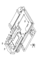
図1は、本発明の実施の形態に係るウエハ検査装置の構成を示す斜視図である。このウエハ検査装置に備えられたウエハ検査用ステージは、ウエハ搬送機能、ウエハアライメント機能、及び外観マクロ検査機能を有する。
【0012】
図1に示すように、基台1には、エレベータユニット2、二本のガイドレール3,3、及び送り機構4が設けられている。また、基台1の上方には図示しないミクロ観察用の顕微鏡装置が設けられている。エレベータユニット2は、図示しない昇降可能なカセット台に、複数の半導体ウエハが収納されたカセット2aが設置されている。
【0013】
二本のガイドレール3,3上には、下ステージとしてYステージ5が載せられている。Yステージ5は、送りねじ41とモータ42とを用いた送り機構4の駆動により、ガイドレール3,3に沿ってY方向へ移動可能である。また、Yステージ5上に二本のガイドレール6,6及び送り機構7が設けられている。二本のガイドレール6,6上には、上ステージとしてXステージ8が載せられている。Xステージ8は、送りねじ71とモータ72を用いた送り機構7の駆動により、ガイドレール6,6に沿ってX方向へ移動可能である。
【0014】
上ステージであるXステージ8上には、二本のガイドレール9,9、回転テーブル10、及びE字形状のマクロ検査用アーム11が設けられている。二本のガイドレール9,9上には、コ字形状の搬送アーム12が載せられている。搬送アーム12は、リニアモータなどの送り機構の駆動により、ガイドレール9,9に沿ってX方向へ移動可能で、図示しないシリンダ機構により昇降可能である。また搬送アーム12は、回転テーブル10、マクロ検査用アーム11の上方を通過してカセット2a内に移動し、カセット2a内から取り出した半導体ウエハを回転テーブル10上に受け渡すために、回転テーブル10及びマクロ検査用アーム11と干渉せずにZ方向へ昇降する構造のものであれば、上ステージと別体に設けることも可能である。
【0015】
回転テーブル10は、図示しない回転機構によりX−Y平面上で回転可能で、Z方向に昇降可能である。マクロ検査用アーム11は、一方の側部111が揺動機構であるモータ13の回転軸により軸支されており、前記回転軸を中心としてX軸周りに揺動可能である。またマクロ検査用アーム11は、図1に示すように回転テーブル10を挟んで搬送アーム12と対峙した状態で図示しない昇降機構により、回転テーブル10及び搬送アーム12と干渉せずにZ方向へ昇降可能である。
【0016】
なお、エレベータユニット2、Yステージ5、Xステージ8、搬送アーム12、回転テーブル10、及びマクロ検査用アーム11は、図示しない制御部の制御により駆動する。
【0017】
次に、以上のように構成されたウエハ検査装置における制御部の制御による動作について説明する。ウエハ搬送時に、マクロ検査用アーム11は水平な状態で、搬送アーム12と回転テーブル10よりも下方に位置している。この状態で、エレベータユニット2のカセット台が所定ピッチでZ方向へ移動することにより、カセットに収納されている検査用のウエハが、搬送アーム12の挿入位置に位置決めされる。
【0018】
次に、搬送アーム12がX方向へ移動してカセット2a内からウエハを取り出し、回転テーブル10の上方まで搬送する。そして、回転テーブル10は上下機構により上昇し、ウエハを搬送アーム12から受け取る。その後、回転テーブル10が回転し、アライメントセンサ14によりウエハのエッジが検出され、このウエハのエッジデータに基づいてウエハに対してアライメントが行なわれる。
【0019】
次に、マクロ検査用アーム11は昇降機構により上昇し、回転テーブル10上のウエハを受け取り、自身の表面にウエハを吸着保持する。その後、マクロ検査用アーム11は揺動機構により、X軸周りに揺動する。これにより、検査者は目視によりマクロ照明下においてウエハの外観マクロ検査を行なうことができる。マクロ検査が終了すると、マクロ検査用アーム11は揺動機構により水平な状態となる。
【0020】
続いて、マクロ検査用アーム11は昇降機構により下降し、回転テーブル10にウエハを受け渡し、さらに下降して初期位置に停止する。回転テーブル10は、マクロ検査用アーム11からウエハを受け取り吸着保持する。その後、Xステージ8が送り機構7によりX方向へ移動するとともに、Yステージ5が送り機構4によりY方向へ移動することにより、検査者は回転テーブル10上に吸着保持されたウエハ上の任意の箇所を顕微鏡装置で検査することができる。アライメント動作は、マクロ検査後に半導体ウエハを回転テーブル10に受け渡した後で行なってもよい。
【0021】
検査が終了すると、Xステージ8が送り機構7によりX方向へ移動するとともに、Yステージ5が送り機構4によりY方向へ移動し、回転テーブル10をカセット2aの前方の受け渡し位置に戻す。そして、回転テーブル10はウエハの吸着を解除するとともに昇降機構により下降し、ウエハを搬送アーム12に受け渡す。その後、搬送アーム12はウエハを吸着保持し、ガイドレール9,9に沿ってX方向に移動し、ウエハをカセットに収納する。
【0022】
続いて、エレベータユニット2のカセット台が所定ピッチZ方向へ移動することにより、カセットに収納されている次の検査用のウエハが、搬送アーム12の挿入位置に位置決めされ、以降、上記と同様の動作が行なわれる。
【0023】
本実施の形態によれば、カセットからウエハを取り出し収納するための搬送アーム12と、回転テーブル10とを顕微鏡検査用のXYステージの上ステージ(Xステージ8)に設けている。これにより、カセットに顕微鏡検査用のXYステージ(5,8)を近接して設けることが可能となり、装置全体の小型化が図れる。また、外観マクロ検査機能を付加させても、E字形状に形成されたマクロ検査用アーム11を回転テーブル10を挟んで搬送アーム12に対向させて配置することにより、カセットと顕微鏡検査用のXYステージ(5,8)との間隔が大きくならず、装置全体の小型化が図れる。また、搬送アーム12によりカセット内に収納された半導体ウエハをミクロ検査用ステージに搬送することができるため、ウエハの受け渡し回数が減少し、受け渡し時のウエハの破損を防ぐことができるとともに、ウエハ搬送時のタクトタイムを短縮できる。また、顕微鏡装置への受け渡しアームが無くなりレイアウト的に余裕ができるため、アーム形状の制約が減り、ウエハを確実に保持できるアーム形状にすることができる。
【0024】
なお、本発明は上記実施の形態のみに限定されず、要旨を変更しない範囲で適宜変形して実施できる。例えば、ウエハがダイシングフレーム(テープフレーム)に貼り付けられた状態の標本であっても、適用できる。
【0025】
【発明の効果】
本発明によれば、装置全体の小型化を図るとともにウエハの受け渡し回数を削減するウエハ検査装置を提供できる。
【図面の簡単な説明】
【図1】本発明の実施の形態に係るウエハ検査用ステージの構成を示す斜視図。
【図2】従来例に係る検査装置の構成を示す斜視図。
【符号の説明】
1…基台 2…エレベータユニット 2a…カセット 3…ガイドレール 4…送り機構 41…送りねじ 42…モータ 5…Yステージ 6…ガイドレール 7…送り機構 71…送りねじ 72…モータ 8…Xステージ 9…ガイドレール 10…回転テーブル 11…マクロ検査用アーム 12…搬送アーム13…モータ 14…アライメントセンサ[0001]
TECHNICAL FIELD OF THE INVENTION
The present invention relates to a wafer inspection device for inspecting a semiconductor wafer.
[0002]
[Prior art]
In general, a wafer inspection apparatus takes out a wafer from a cassette by a linear motion arm, transports the wafer to an aligner, aligns the wafer, mounts the wafer on a swinging stage, performs macro inspection, and further uses a rotating arm to perform a stage of a microscope apparatus. The system is handed over to a micro inspection. In this wafer inspection apparatus, an aligner and a swing stage for macro inspection must be arranged between the cassette and the stage of the microscope apparatus, so that the inspection apparatus becomes large. 2. Description of the Related Art In recent years, the size of semiconductor wafers has become larger and larger, and recently the size has been shifted from an 8-inch size to a 12-inch size.
[0003]
Patent Document 1 is known as a device for reducing the size of an inspection device. FIG. 2 is a perspective view showing the configuration of the inspection device. The loading / unloading means 101 includes a concave-
[0004]
[Patent Document 1]
JP-A-6-229934
[Problems to be solved by the invention]
However, in the inspection apparatus of Patent Document 1 described above, the wafer is taken out of the
[0006]
If a swing stage for macro inspection is provided between the
[0007]
SUMMARY OF THE INVENTION It is an object of the present invention to provide a wafer inspection apparatus capable of reducing the size of the entire apparatus and reducing the number of times of transferring wafers.
[0008]
[Means for Solving the Problems]
In order to solve the problem and achieve the object, a wafer inspection apparatus according to the present invention is configured as follows.
[0009]
The wafer inspection apparatus of the present invention is a wafer inspection apparatus for inspecting a semiconductor wafer, wherein the XY stage includes a lower stage and an upper stage for moving the semiconductor wafer in an XY direction within an inspection area, and is provided on the upper stage. A rotary table that holds the semiconductor wafer by suction, a cassette that stores the semiconductor wafer that is disposed on a movement extension line of the upper stage, and that is disposed close to the XY stage, and a wafer transfer position in front of the cassette. A transfer arm that takes out the semiconductor wafer from inside the cassette and transfers the semiconductor wafer to a position above the rotary stage and transfers the semiconductor wafer to the rotary stage.
[0010]
BEST MODE FOR CARRYING OUT THE INVENTION
Hereinafter, embodiments of the present invention will be described with reference to the drawings.
[0011]
FIG. 1 is a perspective view showing a configuration of a wafer inspection apparatus according to an embodiment of the present invention. The wafer inspection stage provided in the wafer inspection apparatus has a wafer transfer function, a wafer alignment function, and an appearance macro inspection function.
[0012]
As shown in FIG. 1, the base 1 is provided with an
[0013]
On the two
[0014]
On an X stage 8, which is an upper stage, two
[0015]
The
[0016]
The
[0017]
Next, an operation of the wafer inspection apparatus configured as described above under the control of the control unit will be described. During wafer transfer, the
[0018]
Next, the transfer arm 12 moves in the X direction, takes out the wafer from the
[0019]
Next, the
[0020]
Subsequently, the
[0021]
When the inspection is completed, the X stage 8 is moved in the X direction by the feed mechanism 7, and the Y stage 5 is moved in the Y direction by the feed mechanism 4, returning the rotary table 10 to the transfer position in front of the
[0022]
Subsequently, by moving the cassette table of the
[0023]
According to the present embodiment, the transfer arm 12 for taking out and storing a wafer from the cassette and the rotary table 10 are provided on the upper stage (X stage 8) of the XY stage for microscopic inspection. Thus, the XY stage (5, 8) for microscopic inspection can be provided close to the cassette, and the size of the entire apparatus can be reduced. Even when the appearance macro inspection function is added, the cassette and the XY for microscopic inspection can be provided by disposing the
[0024]
The present invention is not limited to the above-described embodiment, and can be appropriately modified and implemented without changing the gist. For example, the present invention can be applied to a specimen in which a wafer is attached to a dicing frame (tape frame).
[0025]
【The invention's effect】
According to the present invention, it is possible to provide a wafer inspection apparatus that can reduce the size of the entire apparatus and reduce the number of times of transferring wafers.
[Brief description of the drawings]
FIG. 1 is a perspective view showing a configuration of a wafer inspection stage according to an embodiment of the present invention.
FIG. 2 is a perspective view showing a configuration of an inspection apparatus according to a conventional example.
[Explanation of symbols]
Reference Signs List 1
Claims (10)
前記半導体ウエハを検査領域内でXY方向に移動する下ステージと上ステージからなるXYステージと、
前記上ステージ上に設けられ前記半導体ウエハを吸着保持する回転テーブルと、
前記上ステージの移動延長線上に配置され、かつ前記XYステージに近接して配置される前記半導体ウエハを収納するカセットと、
前記カセット前方のウエハ受渡し位置において該カセット内から前記半導体ウエハを取り出し、前記回転ステージの上方を通過して前記回転ステージに搬送する搬送アームと、
を備えたことを特徴とするウエハ検査装置。In a wafer inspection apparatus for inspecting a semiconductor wafer,
An XY stage comprising a lower stage and an upper stage for moving the semiconductor wafer in the XY directions within the inspection area;
A rotary table provided on the upper stage and holding the semiconductor wafer by suction,
A cassette that accommodates the semiconductor wafer, which is arranged on a movement extension line of the upper stage, and is arranged close to the XY stage;
A transfer arm that takes out the semiconductor wafer from within the cassette at a wafer transfer position in front of the cassette, and transfers the semiconductor wafer to the rotary stage by passing above the rotary stage;
A wafer inspection device comprising:
Priority Applications (2)
| Application Number | Priority Date | Filing Date | Title |
|---|---|---|---|
| JP2003162121A JP4282379B2 (en) | 2003-06-06 | 2003-06-06 | Wafer inspection equipment |
| CNB2003101165592A CN100472743C (en) | 2002-11-21 | 2003-11-20 | Chip check apparatus |
Applications Claiming Priority (1)
| Application Number | Priority Date | Filing Date | Title |
|---|---|---|---|
| JP2003162121A JP4282379B2 (en) | 2003-06-06 | 2003-06-06 | Wafer inspection equipment |
Publications (3)
| Publication Number | Publication Date |
|---|---|
| JP2004363455A true JP2004363455A (en) | 2004-12-24 |
| JP2004363455A5 JP2004363455A5 (en) | 2006-07-20 |
| JP4282379B2 JP4282379B2 (en) | 2009-06-17 |
Family
ID=34054358
Family Applications (1)
| Application Number | Title | Priority Date | Filing Date |
|---|---|---|---|
| JP2003162121A Expired - Fee Related JP4282379B2 (en) | 2002-11-21 | 2003-06-06 | Wafer inspection equipment |
Country Status (1)
| Country | Link |
|---|---|
| JP (1) | JP4282379B2 (en) |
Cited By (3)
| Publication number | Priority date | Publication date | Assignee | Title |
|---|---|---|---|---|
| CN102445573A (en) * | 2010-09-13 | 2012-05-09 | 东京毅力科创株式会社 | Wafer inspection apparatus and method for pre-heating probe card |
| KR101236286B1 (en) | 2012-09-24 | 2013-02-26 | (주)대상이엔지 | Apparatus for inspecting defect of panel |
| JP2014150109A (en) * | 2013-01-31 | 2014-08-21 | Disco Abrasive Syst Ltd | Decompression processing apparatus |
Families Citing this family (1)
| Publication number | Priority date | Publication date | Assignee | Title |
|---|---|---|---|---|
| CN102275869B (en) * | 2011-08-03 | 2014-04-09 | 苏州大学 | Equipment and method for bonding single chip and wafer |
-
2003
- 2003-06-06 JP JP2003162121A patent/JP4282379B2/en not_active Expired - Fee Related
Cited By (3)
| Publication number | Priority date | Publication date | Assignee | Title |
|---|---|---|---|---|
| CN102445573A (en) * | 2010-09-13 | 2012-05-09 | 东京毅力科创株式会社 | Wafer inspection apparatus and method for pre-heating probe card |
| KR101236286B1 (en) | 2012-09-24 | 2013-02-26 | (주)대상이엔지 | Apparatus for inspecting defect of panel |
| JP2014150109A (en) * | 2013-01-31 | 2014-08-21 | Disco Abrasive Syst Ltd | Decompression processing apparatus |
Also Published As
| Publication number | Publication date |
|---|---|
| JP4282379B2 (en) | 2009-06-17 |
Similar Documents
| Publication | Publication Date | Title |
|---|---|---|
| JP5322822B2 (en) | Wafer prober for semiconductor inspection and inspection method | |
| JP5381118B2 (en) | Probe device | |
| JP5189370B2 (en) | Substrate exchange apparatus, substrate processing apparatus, and substrate inspection apparatus | |
| JP2010067940A (en) | Foup opening/closing device and probe apparatus | |
| JP6300136B2 (en) | Prober | |
| KR101424017B1 (en) | Substrate inspection apparatus | |
| JP3933524B2 (en) | Substrate processing equipment | |
| JP2013214676A (en) | Peeling system, peeling method, program, and computer storage medium | |
| JP4166813B2 (en) | Inspection apparatus and inspection method | |
| US8674712B2 (en) | Apparatus for driving placing table | |
| KR101147787B1 (en) | Probe apparatus and substrate transfer method | |
| JP2002043395A (en) | Wafer transfer system and transfer method thereby | |
| JP4282379B2 (en) | Wafer inspection equipment | |
| JPH02126648A (en) | Treatment apparatus | |
| EP2346073B1 (en) | Prealigner | |
| JP3282787B2 (en) | Wafer transfer mechanism | |
| JP4910033B2 (en) | Probe device | |
| KR20150135920A (en) | Apparatus for inspecting a wafer | |
| JP2013079847A (en) | Substrate inspection apparatus and substrate inspection method | |
| JPH11238767A (en) | Aligner for wafer and contactor | |
| US11894256B2 (en) | Substrate holding mechanism, substrate mounting method, and substrate detaching method | |
| JPH09226987A (en) | Substrate carrier device | |
| JP4949454B2 (en) | Probe device | |
| JP4913201B2 (en) | Substrate transfer method | |
| TW202301538A (en) | Processing apparatus and positioning method |
Legal Events
| Date | Code | Title | Description |
|---|---|---|---|
| A521 | Written amendment |
Free format text: JAPANESE INTERMEDIATE CODE: A523 Effective date: 20060602 |
|
| A621 | Written request for application examination |
Effective date: 20060602 Free format text: JAPANESE INTERMEDIATE CODE: A621 |
|
| A977 | Report on retrieval |
Free format text: JAPANESE INTERMEDIATE CODE: A971007 Effective date: 20061214 |
|
| A131 | Notification of reasons for refusal |
Effective date: 20081216 Free format text: JAPANESE INTERMEDIATE CODE: A131 |
|
| A521 | Written amendment |
Free format text: JAPANESE INTERMEDIATE CODE: A523 Effective date: 20090202 |
|
| TRDD | Decision of grant or rejection written | ||
| A01 | Written decision to grant a patent or to grant a registration (utility model) |
Free format text: JAPANESE INTERMEDIATE CODE: A01 Effective date: 20090224 |
|
| A01 | Written decision to grant a patent or to grant a registration (utility model) |
Free format text: JAPANESE INTERMEDIATE CODE: A01 |
|
| A61 | First payment of annual fees (during grant procedure) |
Free format text: JAPANESE INTERMEDIATE CODE: A61 Effective date: 20090317 |
|
| FPAY | Renewal fee payment (prs date is renewal date of database) |
Free format text: PAYMENT UNTIL: 20120327 Year of fee payment: 3 |
|
| LAPS | Cancellation because of no payment of annual fees |