JP2004358559A - Method of manufacturing article with fine surface structure, and die and method of manufacturing the same - Google Patents
Method of manufacturing article with fine surface structure, and die and method of manufacturing the same Download PDFInfo
- Publication number
- JP2004358559A JP2004358559A JP2003156094A JP2003156094A JP2004358559A JP 2004358559 A JP2004358559 A JP 2004358559A JP 2003156094 A JP2003156094 A JP 2003156094A JP 2003156094 A JP2003156094 A JP 2003156094A JP 2004358559 A JP2004358559 A JP 2004358559A
- Authority
- JP
- Japan
- Prior art keywords
- mold
- resin
- shape
- final product
- dry etching
- Prior art date
- Legal status (The legal status is an assumption and is not a legal conclusion. Google has not performed a legal analysis and makes no representation as to the accuracy of the status listed.)
- Pending
Links
Images


Abstract
Description
【0001】
【発明の属する技術分野】
本発明は、表面に微細加工を施すことによって、光学的機能、機械的機能又は物理的機能を発現する製品の製造や加工に関するものである。このような微細加工は、例えばMLA(マイクロレンズアレイ)、回折光学素子、偏向光学素子、屈折光学系素子、複屈折光学素子、光ファイバー系光学素子、ビームスプリッター等の光学素子の製造に利用することができ、特に外形寸法が10mm以下の光学素子の製造に利用するのに適する。また、この方法は、マイクロマシニング、機械摺動部品(自動車用エンジン、エアコン用コンプレッサーなど)の表面処理方法など、幅広い産業分野に応用・利用可能である。
【0002】
【従来の技術】
A)リソグラフィー技術を用いたマルチレベル素子の作製方法として、M枚のマスクを使って(M−1)回のプロセスでN=2Mレベルのステップ状の位相分布を持つ素子を作製する方法が提案されている(非特許文献1参照)。
【0003】
B)電子ビーム、レーザービームやイオンブーム等を用いた直接描画法と光リソグラフィーとドライエッチング技術を組み合わせた方法も提案されている(非特許文献2参照)。
【0004】
C)濃度分布マスク法によって感光性材料層上に目的の三次元構造を製作し、この形状を最終製品材料にドライエッチングで転写することが提案されている(特許文献1参照)。濃度分布マスクとは、面内のパターンだけでなく、膜厚方向にも透過率分布をもったマスクである。
【0005】
D)あらかじめ金型を製作しこの形状を樹脂転写によって製品材料表面に転写すること、及びその転写後の樹脂形状を最終製品材料にドライエッチングで転写することが提案されている(特許文献2参照)。
【0006】
【非特許文献1】
「光技術コンタクト」誌、Vol.38, No.5 (2000) P.42〜51、特にP.45
【非特許文献2】
「応用物理」誌、第68巻第6号(1999)、P.633〜638
【特許文献1】
特開2001−356470号公報
【特許文献2】
特開2002−192500号公報
【0007】
【発明が解決しようとする課題】
Aの方法では、マスク枚数が多く必要であること、アライメント回数が多くその誤差が無視できないこと、深さ方向のエッチング誤差が無視できないこと、最小ライン幅は1μm程度が限界であること、等が問題である。
【0008】
Bの方法では、高精度な制御技術を有する装置が必要で、装置が高価であること、描画に時間が非常にかかり(500μm×500μmの正方形で10〜15時間程度)、量産性が全くない、再現性に乏しい、等の問題があり、実用化された例はない。
【0009】
高精度の表面3次元構造を再現性よく製作するという課題に対しては、上記のCの方法とDの方法はよくその課題を達成することができる。また、金型を使用して転写するDの方法は、製造コストを低下させる利点も備えている。
【0010】
本発明は、上のDの方法の改良に係り、三次元構造物の高さを高くすることを容易にすることを目的とするものである。三次元構造物の高さを高くすることは、光学レンズの場合であればその開口数(NA)を大きくして、レンズを明るくすることを意味している。
本発明はまた、金型の寿命を長くすることも目的としている。
【0011】
【課題を解決するための手段】
本発明は、以下の工程(A)から(F)を備えて表面に凸状又は凹状の微細構造をもつ物品を製造する製造方法である。
(A)最終目的とする前記微細構造の大きさを縮小した構造を表面に有するプレ構造を最終製品材料に製作する工程、
(B)最終目的とする前記微細構造にほぼ一致した大きさで、前記微細構造とは凹凸を反転した微細形状を表面に有する金型の表面に離型処理を施す工程、
(C)離型処理の施された前記金型の表面と前記プレ構造を製作した最終製品材料の表面との間に硬化可能な樹脂を介して前記金型に最終製品材料を押し当て、前記金型の表面形状の反転形状をその樹脂に転写する工程、
(D)工程(C)における転写後の前記樹脂を硬化させる工程、
(E)工程(D)で硬化した後の前記樹脂を最終製品材料に接合させた状態でその樹脂を前記金型から剥離させる工程、及び
(F)工程(E)の後に前記最終製品材料上に存在する前記樹脂に転写された形状をドライエッチング法によって前記最終製品材料に転写する工程であって、前記プレ構造を最終目的構造の大きさに拡大するドライエッチング条件で転写する工程。
【0012】
目的基板上に微細形状を製作する方法は種々あるが、ドライエッチング法で製作する場合、目的とする形状の高さが高いほど製作は難しくなる。その理由は、高さが高くなるほどエッチング量が多くなり、これに伴って加工時間が長くなり高精度形状製作が加工時間に指数関数的に比例して難しくなる為である。そこで、本発明では、目的とする形状にほぼ近い構造を有する微細形状をもつプレ構造を予め製作し、ドライエッチングの加工時間を相対的に短縮する。
【0013】
また金型を製作する方法は種々あるが、これも目的とする形状の高さが高いほど製作は難しくなる。そこで、本発明では、目的とする形状にほぼ近い構造を有する微細形状をもつ金型を製作する。そして、その後のドライエッチングによる転写工程で高さを高くするように条件を設定することにより、最終目的構造の形状の高さは金型の形状よりも高くなる。
【0014】
本発明で樹脂に転写するために用いる金型は、基になる金型から樹脂転写を経て形成された中間金型も含んでいる。
本発明では、金型又は中間金型の表面を離型処理するので、樹脂が金型又は中間金型から容易に剥離する。また、これにより、金型及び中間金型の寿命が伸び、かつ転写性が向上する。
また、プレ構造と金型とは、予め初期に設けられた位置合わせ用のトンボと称されるマークで位置合わせし、光学軸が合致するように製作する。
【0015】
【発明の実施の形態】
プレ構造は最終的な製品に比べて微細構造の精度は要求されない。そのため、種々の方法により形成することができる。その方法を例示すれば、次の通りである。▲1▼サンドブラスト法、▲2▼ドライエッチング法、▲3▼ウエットエッチング法、▲4▼ダイシング法、▲5▼研削法、▲6▼切削法、▲7▼成膜法(真空蒸着、スパッタリング、CVDなど)、▲8▼ゾル−ゲル法、▲9▼ガラス接合法などである。このうち、サンドブラスト法とウエットエッチング法は実施例で詳述する。ドライエッチング法はリソグラフィーとドライエッチングにより基板表面にプレ形状を形成する方法である。ダイシング法、研削法及び切削法は基板表面を機械的に加工してプレ形状を形成する方法である。成膜法は基板から離した位置にマスクを配置することにより、基板上に凸形状のプレ形状を形成する方法である。ゾル−ゲル法は、テトラアルキルオルソシリケートを用い、加水分解と重縮合によって調製された溶液をプレ形状のパターンに塗布し、乾燥して溶媒を取り除いた後、熱処理を行ないシロキサン結合を完全にすることでシリカガラスによりプレ形状を形成する方法である。ガラス接合法は、別途パターンを形成したガラス基板のパターン面をHF溶液又は水により最終目的基板表面に接合し、真空中で放置した後、250℃で10分間又はそれ以上加熱して接合させ、その後その接合したガラス基板を裏面側から研磨してパターンを露出させることにより、そのパターンによりプレ形状を形成する方法である。
金型の表面形状の反転形状を転写する樹脂としては、紫外線硬化型樹脂や熱硬化型樹脂を用いることができる。
【0016】
その転写用樹脂として紫外線硬化型樹脂を用いる場合には、次のような利点がある。
▲1▼常温での硬化が可能である。
▲2▼液体状で塗布できるので、流動性がよく、泡などの発生を防ぐことができる。
▲3▼紫外光を均一に照射して硬化させることができるので、均一に硬化させることができる。
▲4▼短時間に硬化させることができる。
▲5▼紫外線硬化型樹脂は、収縮量の小さい樹脂が多く開発され、採用の範囲が広い。
▲6▼「耐プラズマ性を有する分子設計」の自由度が高い。
【0017】
その結果、紫外線硬化型樹脂を用いると、金型の表面形状をより正確に容易に転写することができるようになる。
また、その転写用樹脂として熱硬化型樹脂を用いる場合でも、均一に硬化させることによって、紫外線硬化型樹脂と同様に金型や中間金型の表面形状を正確に転写することができる。熱硬化型樹脂としては、プラスチック眼鏡レンズや、コンタクトレンズの製造に使用されている樹脂を用いることができる。そのような熱硬化型樹脂を用いた成型方法は注型法と呼ばれており、金型に液体状の熱硬化型樹脂を流し込み、徐々に加熱して24時間程度の時間をかけて硬化させる。
【0018】
金型製作に関し、金型表面の微細形状が1mmより大きい寸法であれば、通常市販されている高精度機械加工(NC旋盤、NC超精密加工機等)によって加工することも可能である。
また、金型表面の微細形状が1mm以下の寸法であれば、発明者らが提案している方法(特許文献1参照。)で製作することができ、あるいは、ガラスや金属材料をリソグラフィーとウエットエッチングにより製作することも可能である。
【0019】
金型表面の微細形状が10μm以下というようなごく微細な寸法であれば、発明者らが既に提案している方法(特許文献2参照。)により、金型母材料に形成されたレジスト(感光性材料)に電子線(EB)又はレーザービームにより所望の形状を描画し現像して微細構造を形成し、その微細構造をドライエッチングにより金型母材料に転写することにより製作することが可能である。
【0020】
この方法は以下の工程(a)から(c)を含む。
(a)金型母材料表面上に感光性材料を塗布する工程、
(b)前記感光性材料に濃度分布マスクを使用して露光し、次いで現像して前記感光性材料に所望形状を形成する工程、及び
(c)前記感光性材料の形状をドライエッチング法によって前記金型母材料に転写する工程。
このように、レジストの形状をドライエッチング法によって金型母材料に転写するようにすれば、軟質材料であるレジストの形状を硬質金型材料に転写できる。
【0021】
また、本発明で使用する金型には中間金型も含むが、中間金型は以下の工程(a)から(e)を含んで製作することができる。
(a)基になる他の金型の表面に離型処理を施す工程、
(b)離型処理の施された前記金型の表面と金型母材料の表面との間に硬化可能な樹脂を介して前記金型に金型母材料を押し当て、前記金型の表面形状の反転形状をその樹脂に転写する工程、
(c)工程(b)における転写後の前記樹脂を硬化させる工程、
(d)工程(c)で硬化した後の前記樹脂を前記金型母材料に接合させた状態でその樹脂を前記金型から剥離させる工程、及び
(e)工程(d)の後に前記金型母材料上に存在する前記樹脂に転写された形状をドライエッチング法によって前記金型母材料に転写する工程。
【0022】
ドライエッチング法により金型を製作する場合、金型母材料はドライエッチング可能な材料であることが必要であり、そのような材料として金属材料、ガラス材料、セラミックス材料、プラスチック材料、硬質ゴム材料などを用いることができる。
【0023】
硬化型樹脂として紫外線硬化型樹脂を使用し、金型を介して紫外線を樹脂に照射する場合には、金型を形成する材料としては、合成石英や耐熱ガラスなど、耐熱性で、紫外線硬化型樹脂を硬化させるための波長に対して光透過性の性質をもつものが好ましい。耐熱ガラスとしては、パイレックス(登録商標)やネオセラム(登録商標)などを使用することができる。
【0024】
金型を製作する際、感光性材料の形状をドライエッチング法によって金型母材料に転写する工程におけるドライエッチング工程で、所望の形状を転写するために、選択比を段階的又は連続的に変化させることが好ましい。このように、選択比を段階的又は連続的に変化させることにより、転写時に所望の形状を得ることができるようになる。
【0025】
金型表面の離型処理の一例は、金型や中間金型の表面に金属薄膜を成膜することであり、その金属薄膜はNi,Cr,Fe,Al,Co,Cu,Mo,Pt,Au,Nb、Tiなどの単一金属又は複合材料からなるものとすることができる。この離型処理により、金型の形状転写性が飛躍的に増し、正確な転写が行なえると同時に、剥離性が容易となり金型や中間金型の寿命が飛躍的に向上する。
【0026】
離型処理として、さらにその金属薄膜上に微細な構造のフッ素樹脂を含む層によって表面処理を施すことが好ましい。この表面処理はフッ素樹脂を含む層をメッキ方法や蒸着方法によって形成することにより行なうことができる。
金型表面への他の離型処理方法として、金型や中間金型の表面にフッ素官能基を有する有機化合物層を形成する方法も好ましい。
【0027】
金型表面形状の反転形状を転写する樹脂として紫外線硬化型樹脂を使用する場合、紫外線硬化型樹脂を硬化させる方法として、金型と最終製品材料の2材料のうち少なくとも一方はその紫外線硬化型樹脂を硬化させうる波長域の光に対して光透過性である材料を使用する。そして、その紫外線硬化型樹脂の硬化工程では、一方の材料のみが光透過性材料である場合にはその光透過性材料を通して、両方の材料が光透過性材料である場合には一方又は両方の光透過性材を通してその紫外線硬化型樹脂に光照射してその紫外線硬化型樹脂を均一に硬化させるようにするのが好ましい。紫外線硬化型樹脂を均一に硬化させることにより、金型の形状転写性が飛躍的に増し、正確な転写が行なえる。
【0028】
金型の表面形状の反転形状を転写する樹脂として熱硬化型樹脂を使用する場合、熱硬化型樹脂を硬化させる方法として、金型と最終製品材料を位置決めした状態で固定し、樹脂注入口を別途設けて、その樹脂注入口から熱硬化型樹脂を金型と最終製品材料との間に注入する。熱硬化型樹脂の硬化工程では徐々に加熱しながら熱硬化型樹脂を挟み込んでいる金型と最終製品材料の全体に均一に熱が行きわたるようにして加熱硬化させるのが望ましい。
【0029】
一般に、樹脂は硬化の際に収縮するものである。そこで、樹脂の収縮量を予め求めておき、その樹脂に形状を転写する金型の製作工程では、その収縮量を見込んで金型の形状が深くなるように補正して加工するのが好ましい。これにより、硬化収縮量の補正が可能となる。
【0030】
離型処理の施された金型の表面に樹脂を介して最終製品材料を押し当てる際、樹脂と最終製品材料表面との間に両者の密着性を向上させるためのシランカップリング剤処理等のプライマー表面処理を施しておくことが好ましい。これにより、剥離工程で金型側から選択的に剥離が行われ、樹脂のクワレ(剥離の際に樹脂の一部が金型に残ること)が急激に減少する。
【0031】
その結果、次工程での形状転写性が向上する。また、金型の表面に樹脂を介して最終製品材料を押し当てる際、金型の表面と最終製品材料との間にギャップ(スペース)を設けることが重要である。このギャップは、樹脂が硬化する際の収縮分を周りから供給する流路として使用することができる。その方法として、金型には、対向して張り合わされる材料面との間に樹脂の収縮に伴う体積減少分を周囲の樹脂から供給するための流路を形成する複数の凸部を目的構造の周囲に形成するのが好ましい。
【0032】
樹脂に転写された形状をドライエッチング法によって最終製品材料に転写する際、最終製品材料に所望の形状を形成するためにそのドライエッチングにおける樹脂と最終製品材料とのエッチングの選択比を段階的又は連続的に変化させることが好ましい。この選択比の調整により形状の補正が可能となり、所望の形状に転写できるようになる。
【0033】
この最終製品材料への転写では、樹脂層の最大厚さ量を最終製品材料に転写する。最終製品材料にはプレ構造が形成されているため、樹脂層の最大厚さ量は最終製品材料の凹凸の高さに比べると小さく、そのために必要なエッチング時間は短かくてすむ。
【0034】
【実施例】
(実施例1)
図1に示す対向ファイバー結合光学素子2を製作した。この結合光学素子2は合成石英材の両面に形成された直径Φ0が約0.784mm、高さH0が40μmのレンズで、同心円状に非球面形状を配列したものである。(A)はこの結合光学素子2を光源側に配置した状態を示すものであり、光ファイバ4aからの光をこの結合光学素子2が集光して受ける。(B)はこの結合光学素子2を受光側に配置した状態を示すものであり、この結合光学素子2で受光した光を集光して光ファイバ4bに導く。6a,6bはそれぞれ光ファイバ4a,4bの先端に配置された石英平板である。
【0035】
光通信用光学素子の最終目的構造は合成石英材の両面上にそれぞれ210個(=15×14)形成された直径が0.784μmのレンズである。その曲率半径は、1.8897mm、高さは40.0μmである。
この結合光学素子2は図2に示されるようなマイクロレンズアレイ8として形成されている。図2で、(A)は平面図、(B)はそのX−X線位置での断面図である。このマイクロレンズアレイ8は、有効レンズ数が12行×13列=156個で、レンズ配置のピッチPが1.1mmである。なお、最外周のレンズは、光学性能調整用レンズとして配置しているのみで、実際には使用しない。
【0036】
次にこの光学素子の製作手順を示す。
先ず、プレ形状を製作した。
図3はプレ形状を製作するためのレジストパターンを形成する工程を示したものである。
予め図2のレンズ配置に合致する部分を遮光する露光用マスクを用意する。ここで用意するマスクの遮光部分の直径は、最終目的レンズ形状とほぼ同径である。
【0037】
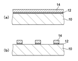
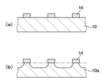
(a)石英基板10上に200nm厚さのCr金属膜をスパッタリング法で成膜する。さらに、そのCr金属膜上に感光性レジスト材料(東京応化製 OFPR−5000−500)14を5μmの厚さで均一にスピンコーターで塗布し、所定の条件でプリベーク(ホットプレート上で130℃×100秒)した。
【0038】
(b)その後、上記マスクで露光した後、現像とリンスを行なった後、オーブンでポストベーク(150℃×60分)して、レジストパターン14を形成した。
ついで、そのレジストパターン14をマスクとしてCr金属膜12をウエットエッチング液でエッチングしてレジスト部以外の部分を除去した。この際、Cr金属膜12の断面は、ウエットエッチング時のアンダーカットによって断面が斜めにエッチングされている。
【0039】
図4はサンドブラスト法によりプレ形状を形成する工程を示したものである。
(a)上記のようにレジストパターン14とCr金属膜パターン12が形成された石英基板10上に市販のサンドブラスト装置を使用して粒径(メッシュ#500)のサンドブラスト材を垂直方向上方から空気圧を利用しながら吹き付ける。
【0040】
(b)これによって、石英基板材料10は物理的な衝撃によってサンドブラスト材料と共に次第に削られていく。ただし、▲1▼垂直上方から進入してくるブラスト材料と下方から上方に取り除かれる「ブラスト材料及び石英紛」の衝突が生じる。この現象によって、深く掘られる程に凸部11の先端部が狭く(細く)なる現象が生じる。また、▲2▼基板10上面のレジスト材料14は、サンドブラスト材料の衝撃に次第に耐えられず削れて行く。同様にCr金属膜12も次第に削れて行く。Cr金属膜12の断面は、ウエットエッチング時のアンダーカットによって断面が斜めにエッチングされているのでサンドブラストによる削られ方も斜めに進行し、しかもテーパーが増長されるように斜面が現れる。上記方法によって、形成されるプレ形状は、凸部11の先端部が直径0.2mmの平坦面を有し、基部の直径Φ1が約0.76mm、高さH1が約30μmのぼぼ球面形状を有する凸アレイ形状の石英基板10aを得ることができた。この凸部11は、最終目的のレンズの直径Φ0、高さH0に比べて縮小されたサイズになっている。
サンドブラスト法で製作したプレ構造は、表面が荒れているためそのままでは光学的には使用できない。
【0041】
金型は図5に示す進め方で製作した。
本実施例では凹金型を使用する。その凹金型としてネオセラム製の金型を製作し使用した。以下に製作手順の概要を示す。
先ず、本件製品の製作に当たっては、次の進め方で製作した。
(1)目的高さ:40.0μmの20.5/40.0の高さ(0.5125倍の縮小構造。すなわち、n=1.951)の凸形状金型をシリコン基板上に製作することにした。
【0042】
金型母材料20として直径が6インチ、厚さが0.625mmのシリコン基板を用意した。この金型母材料20の表面上に感光性材料(レジスト)(東京応化社製:TGMR−950)をスピンナーにて、1000rpmで塗布した。このときのレジスト膜厚は、25.0μmであった。次いで、ホットプレート上で100℃にてベーク時間180秒でプリベークした。
【0043】
次に予め用意した濃度分布マスク(目的の構造で、かつ高さが20.5μmになるように予め設計している。塗布後のレジスト厚さは、露光・現像。リンス工程を経ると、露光されなかった箇所も膜べりし、膜厚が薄くなる。)を使用してステッパーで2000mJ照射した。
シリコン基板に形状を転写する際は、選択比は1.2とする。シリコン基板に形状を転写した後は、高さが24.6μmとなった。
【0044】
(2)次いで、シリコン基板に形状を転写した後に、別途用意したネオセラム中間材料に金型を転写して凹形状中間金型を得る。この際の、ドライエッチング時の選択比は1.4で転写した(ここで、樹脂の収縮率が4%であるので、シリコン金型の高さ24.6μmが樹脂に転写されて24.6μm×0.96=23.6μmとなり、それが選択比1.4でネオセラム中間材料に転写されるので、転写後の高さは、23.6μm×1.4=33.0μmとなる。)。このときの形状は、反転し、凹形状である。
【0045】
(3)最後に、最終製品材料である石英材料に上記中間金型形状を転写する。この際のドライエッチング時の選択比は1.29で転写した(ここで、樹脂の収縮率が4%であるので、ネオセラム中間金型の高さ33.0μmが樹脂に転写されて33.0μm×0.96=31.7μmとなり、それが選択比1.29で最終製品材料に転写されるので、転写後の高さは、31.7μm×1.29=40.9μmとなる。)。このときの形状は、正転して凸形状である(中間金型に対しては、反転している)。
【0046】
図6、図7の(A)から(H)の図を用いて、この光学素子の製作手順をより詳細に説明する。なお、図6、図7では説明簡略化のために、独立のレンズを2個製作する例を示しているが、156個のレンズを製作する場合も事情は全く同一である。
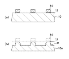
(A)金型母材料411として直径が6インチ、厚さが0.625mmのシリコン基板を用意した。金型母材料411の上にCr膜414をスパッタリング法で800Åの厚さに成膜し、フォトリソグラフィー法とエッチングにより、目的光学レンズを形成する領域の周囲のCr膜を円形に沿って部分的に抜いた部分415を、例えば、円形の外周に沿って6点形成する。
【0047】
この部分415が、中間金型から最終製品材料に形状転写する工程での樹脂の流路のためのスペーサとなる。すなわち、この部分415は後で説明する工程(E)の図でのスペーサ用凸部455に対応して、この部分415が周囲よりも高い凸状態となる。
【0048】
Cr膜414をもつ金型母材料411の表面上に感光性材料(レジスト)(東京応化社製:TGMR―950)をスピンナーにて塗布した。このときのレジスト膜厚は、25.0μmであった。次いで、100℃にてベーク時間180秒でプリベークした。
【0049】
次に、濃度分布マスク(目的の構造で、かつ高さが20.5μmになるようにあらかじめ設計している)を使用してステッパーで2000mJ照射した。
その後、現像、リンス後、UVハードニング処理を施してレジストパターン412,413を形成した。その状態が図6(A)である。413はシリコン金型から中間金型に形状転写する工程での樹脂の流路確保用のスペーサのためのレジストパターンである。目的の光学素子用レジストパターン412(1/nに縮小)の高さは、その流路確保用スペーサのためのレジストパターン413よりも0.2μmほど低くなっている。
【0050】
(B)次に、そのレジストパターン412,413及びCr膜パターン414をドライエッチング法によって金型母材料411に転写した。このときのドライエッチングは、TCP(誘導結合型プラズマ)エッチング装置を用い、CHF3:5.0sccm、CF4:10.0sccmのガスを導入しながら、基盤バイアス電圧:500W、上部電極パワー:1250W、真空度1.5×10⁻³Torr(すなわち1.5mTorr)で21分間エッチングを行なった。このときのエッチング速度は、0.8μm/分であった。僅かにオーバーエッチングで終了させた。エッチングの選択比(金型母材料であるシリコンのエッチング速度/レジストのエッチング速度)は1.4で、エッチング後の光学レンズ部422の高さは28.7μm(=20.5×1.4)であった。表面粗さは、Ra=0.001μm以下で良好であった。この形状高さは、次工程での樹脂の収縮を見込んでいない。ここでは、次工程での樹脂用流路を確保するために、マスク露光の際に光学レンズ部422の外周側にシリコン金型411aに凸形状のスペーサ423を形成し、十分な樹脂流路を確保したためである。
【0051】
425はシリコン金型411aに形成された凹部であり、工程(A)でCr膜が除去されていた部分415に該当している。凹部425は最下点部となっており、(シリコン/レジスト)の選択比よりも(シリコン/Cr膜)の選択比の方が大きいので、その凹部425はCr膜厚さ:800Åの約3倍の0.2μm程度に深くエッチングされている。
【0052】
このときのシリコン金型411aの光学レンズ部422の形状は、露光上がりのレジストパターン412の形状と同様の形状であった。
このシリコン金型411aの表面を離型処理するために、実施例1と同様にフッ素官能基を有するトリアジンチオール有機化合物を1000Å成膜して表面処理した。
【0053】
(C)次に、離型処理したシリコン金型411aを光学レンズ部422が形成された面が上側を向くようにセットして、この上に紫外線硬化型樹脂としてアクリル系樹脂434(大日本インキ社製:GRANDIC RC−8720)を3cc塗布した。
【0054】
このシリコン金型411aを専用の接合機にセットし、予め別の工程でシランカップリング処理(密着性向上処理)を施した、平板状中間材料431(日本板硝子製:ネオセラム(登録商標))の平面をゆっくりと押し当てる。このとき、紫外線硬化型樹脂434の中に泡が発生しないように降下速度を制御した自動接合機で接合した。
【0055】
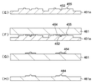
次に、シリコン金型411a側からゆっくりと中間材料431側に押し上げて、形状転写時に余分となる紫外線硬化型樹脂434を基板外周部から除去した。更に、中間材料431の裏面側から均一な紫外線光を4000mJ照射して紫外線硬化型樹脂層434を硬化させた。紫外線照射は、光学素子中心部分から行なった。このとき、樹脂434は体積収縮するが、スペーサ423で中間材料431が押えられている(下方に低下するのを防いでいる)ため、樹脂収縮による体積減少を周りの樹脂が補うように移動する。したがって、体積の収縮、高さの差は生じない。硬化後の紫外線硬化型樹脂層434の厚さは、0.1μm以下であった。紫外線硬化型樹脂層434の最大厚さは、「パターン深さ28.7」+「トップ層間隔0.1」=28.8μmである。
【0056】
(D)次に、紫外線硬化型樹脂層434を中間材料431に接合したままシリコン金型411a表面から剥離するために、治具を使って、剛性の低いシリコン基板(シリコン金型411a)をやや凸形状に変形させながら剥離させた。シリコン金型411aを樹脂434から剥がすと、中間材料431上に残った樹脂434にシリコン金型411aの表面形状が反転して転写されている。シリコン金型の光学レンズ部422は凹部442となり、シリコン金型の凹部425はスペーサ用凸部445となっている。
【0057】
中間材料431表面上の樹脂層434の転写形状を測定したところ、光学素子部442の深さ(凹形状)は、27.6μmに小さくなっていた。これは、樹脂層434が硬化収縮した為であった(ここで、樹脂の収縮率が4%であるので、28.7μm×0.96=27.6μmである。)。
【0058】
(E)次に中間材料431上の樹脂層434の形状を上記と同様にドライエッチング法により中間材料431に転写した。ドライエッチング条件は、TCPエッチング装置を用い、CHF3:15.0sccm、CF4:15.0sccm、Ar:10.0sccmのガスを導入しながら基盤バイアス電圧:500W、上部電極パワー:1250W、真空度1.5×10⁻³Torr(すなわち1.5mTorr)で、51分間エッチングを行なった。この時のエッチング速度は0.80μm/分であった。
【0059】
エッチングの後半ではCHF3ガス量を4.0sccm増加させて選択比を若干大きくしてエッチングした。選択比を段階的に変更することによって、転写時に所望の形状を得ることができた。エッチングの選択比は平均で1.5であり、エッチング後の形状の高さは、40.0μmであった。表面粗さは、Ra=0.001μm以下で良好であった。
【0060】
これにより、レンズ用凹部452と、次の形状転写工程の際に樹脂の流路を確保するスペーサ用凸部455とを備えた中間金型431aが得られた。このときの中間金型431aの形状は、シリコン金型411aに比較して、ピッチが一定で、高さだけが1.95倍(40.0μm/20.5μm)になっていた。
【0061】
この中間金型431aの表面を離型処理するために、中間金型431aの表面をフッ素官能基を有するトリアジンチオール有機化合物で表面処理した。これは、有機鍍金法と言われる方法で行なった。具体的には、フッ素化SFTTの末端機に−OH基を有する化合物を溶媒に溶かした溶液中で電解重合処理して、中間金型431a表面にフッ素系の有機薄膜を形成した。この条件で1000Å成膜した。中間金型431aのネオセラムと石英は、材料の主成分がともにSiO2であるため、同様の離型処理で対応可能である。
【0062】
(F)次に、離型処理した中間金型431aを、その形状を持つ面が上側を向くようにおき、その上に紫外線硬化型樹脂464としてアクリル系樹脂(大日本インキ社製:GRANDIC RC−8720)を3cc塗布した。紫外線硬化型樹脂464はレンズ部に多めに塗布する。
【0063】
この中間金型431aを専用の接合機にセットし、その樹脂の上から、図3で説明したようにプレ構造を形成し別の工程でシランカップリング処理(密着性向上処理)を施した最終製品用の石英材料基板(信越石英社製:合成石英)461をゆっくりと押し当てる。このとき、紫外線硬化型樹脂464の中に泡が発生しないように降下速度を制御した自動接合機で接合した。これにより、中間金型431aと平面基板461間に紫外線硬化型樹脂464が挟持された状態となる。
【0064】
次に、中間金型431a側からゆっくりと最終製品材料(石英)461側に押し上げて、形状転写時に余分となる紫外線硬化型樹脂464を基板外周部から除去した。
次に、最終製品材料461の裏面側から均一な紫外線光を3000mJ照射して紫外線硬化型樹脂層464を硬化させた。この場合も紫外線照射は、光学素子中心部分から行なう。このとき、樹脂464は体積収縮するが、スペーサ455で最終製品材料461が押えられている(下方に低下するのを防いでいる)ため、樹脂収縮による体積減少を周りの樹脂が補うように移動する(図ではスペーサ455が樹脂を密封しているように見えるが、スペーサ455は部分的にのみ形成されており、樹脂は移動が可能な構造となっている。したがって、体積の収縮、高さの差は生じない。
硬化後の紫外線硬化型樹脂層464の厚さ(光学素子部以外の部分)は、0.1μm以下であった。紫外線硬化型樹脂層464の最大厚さは、「パターン深さ38.4」+「トップ層間隔0.1」=38.5μmである。
【0065】
(G)次に、紫外線硬化型樹脂層464を最終製品材料461に接合したまま中間金型431aの表面から剥離するために、治具を使って剥離させた。
最終製品材料461表面上の樹脂層464の形状を測定したところ、光学素子部の高さ(凸形状)は、9.8μmに小さくなっていた。
【0066】
(H)次に最終製品材料461上の樹脂層464の形状を上記と同様にドライエッチング法により最終製品材料461に転写した。ドライエッチング条件は、TCPエッチング装置を用い、CHF3:10.0sccm、CF4:24sccm、Ar:5.0sccmのガスを導入しながら、基盤バイアス電圧:500W、上部電極パワー:1250W、真空度1.5×10⁻³Torr(すなわち1.5mTorr)で13.5分間エッチングを行なった。この時のエッチング速度は、0.78μm/分であった。
【0067】
エッチングの後半ではオートプレッシャーコントローラ(APC)装置を使用し、全圧力を3mTorrから1.0mTorrまで連続して低下させて選択比を経時的に大きくしてエッチングした。選択比を段階的に変更することによって、転写時に所望の形状を得ることができた。エッチングの選択比は平均で1.04であり、エッチング後の形状の高さは、40.0μmであった。表面粗さは、Ra=0.001μm以下で良好であった。
【0068】
このようにして図1,2に示した光学素子2が基板の片面に形成される。
他方の面の光学素子2は、一方の面の光学素子2が形成された後、その形成済みの光学素子2を治具やマスクで保護した状態で、基板の他方の面に上記と同じ手順により光学素子2を形成する。
このとき、両面の光学素子2,2の位置決めは、予め設けた位置決めマークを基づいて行なう。
【0069】
(実施例2)
実施例1と同様に、図1,2に示す対向ファイバー結合素子を製作した。
【0070】
この実施例では、プレ形状を図9の方法により製作した。以下に、まずプレ形状の製作方法を説明する。
(a)予め図2のレンズ配置に合致する部分を遮光する露光用マスクを用意する。ここで用意するマスクの遮光部分の直径は、最終目的レンズ形状の目的形状とほぼ同径である。
【0071】
石英基板10上に感光性レジスト材料(東京応化製 OFPR−5000−500)14を5μmの厚さで均一にスピンコーターで塗布し、所定の条件でプリベーク(ホットプレート上で130℃×100秒)した。
その後、上記マスクを使用して露光した後、現像とリンスを行なってレジストパターン14を形成した後、オーブンでポストベーク(150℃×60分)した。
次いで、石英基板10を専用治具に固定する。この固定の目的は、▲1▼専用装置でエッチングするためと、▲2▼石英基板10の裏面保護のためである。
【0072】
(b)次いで、専用のウエットエッチング装置でエッチング(HF)液で石英基板10をウエットエッチングしてレジスト部14以外の部分をエッチングした。このウエットエッチング装置では、石英基板10は、回転機構により回転させられ、▲2▼エッチング液は一定濃度に濃度管理され、十分な流速を有するノズルから噴射される。
【0073】
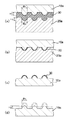
このエッチングによりプレ形状基板10aが得られるが、そのプレ形状基板10aのエッチングされた部分の断面は、図9(b)に示すように、エッチングによるアンダーカットによってできる斜面と、十分攪拌されていたことによる底面の平坦面とから構成されている。
【0074】
上記方法によって、形成されるプレ形状基板10aは、先端部が直径0.2mmの平坦面を有し、基端部が直径約0.5mm、高さが約30μmの概略球面形状を有するアンダーカット形状の凸アレイ形状のものを得ることができた。ただし、実施例1のサンドブラスト法で製作したプレ構造よりもアンダーカット量の分だけ目的形状からは外れている。また、表面が荒れているため、そのままでは光学的には使用できない。
金型は実施例1で使用したのと同じ金型を使用した。
【0075】
光学素子の最終製作手順は、実施例1と同様に、図8に示された手順で行なった。
(a)紫外線硬化型樹脂30としては、実施例1と同様にアクリル系樹脂(大日本インキ社製:GRANDIC RC−8720)を3cc塗布した。
【0076】
(b)紫外線硬化型樹脂30の硬化工程では、これも実施例1と同様に、石英材料10aの裏面側から均一な紫外線光を5分かけて3000mJ(300秒×10mW)照射して紫外線硬化型樹脂層30を硬化させた。
硬化後の紫外線硬化型樹脂層30の3次元構造のトップ位置での厚さ、すなわち紫外線硬化型樹脂層30の3次元構造のトップと石英材料10a間の距離は、約10μmであった。またこのときの紫外線硬化型樹脂層30の3次元構造の斜面での厚さ、すなわち紫外線硬化型樹脂層30の3次元構造の斜面と石英材料10aの凸部との距離は最大値で約12.2μmであった。したがって、紫外線硬化型樹脂層30の最も厚い部分は、プレ構造石英材料10aの斜面部分(約12μm)である。
【0077】
(c)次に、紫外線硬化型樹脂層30を石英材料10aに接合したまま金型20aの表面から剥離するために、治具を使って、剛性の低いシリコン金型20aをやや凸形状に変形させながら剥離させた。
次に、石英材料表面上の樹脂層30の転写形状を測定したところ、光学素子部の高さ(凸形状)は、11.60μmに小さくなっていた。これは、樹脂層30が硬化収縮した為であり、その硬化収縮率は平均で約5%であった。ゆっくりと長時間照射したことにより収縮率が低減できた。このときの高さを光学式(非接触)形状測定機で正確に測定し、後の(d)工程での選択比、及びエッチング条件(経時的な選択比の変更)を適切に設定することが重要である。しかし、実施例1に比較して、斜面部分の樹脂が収縮したことにより目的形状とのズレ量が大きくなった。
【0078】
(d)次に石英材料10a上の樹脂30の転写形状を、実施例1と同様にドライエッチング法により石英材料10aに転写して最終製品を得た。そのドライエッチング条件は、TCPエッチング装置を用い、CHF3:12.0sccm、CF4:4sccmのガスを導入しながら基板バイアス電圧:500W、上部電極パワー:1250W、真空度1.0×10⁻³Torr(すなわち1.0mTorr)で30.0分間エッチングを行なった。この時のエッチング深さは、13μmで、エッチング速度は、0.43μm/分の条件でゆっくり加工した。
【0079】
エッチングの後半ではCHF3ガス量を2.0sccm増加させて選択比を若干大きくしてエッチングした。選択比を4段階的に変更することによって、転写時に所望の形状を得ることができた。エッチングの選択比(石英材料のエッチング速度/樹脂層のエッチング速度)は平均で1.05であり、エッチング後の最終製品の表面形状の高さは、40.0μmであった。表面粗さ(Ra)は、Ra=0.001μm以下で良好であった。尚、光学面は非球面形状を有していた。
【0080】
このときの最終製品の形状は、樹脂転写後の形状に比較して、ピッチが一定で、高さだけが1.05倍になっていた。目標形状が達成できた。
実施例1と同様に、基板10の両面に上記の工程を繰り返して光学素子を形成することにより、図1,2に示された最終製品を得た。
【0081】
(実施例3)
以下に、図8を参照して光学素子の最終製作手順を示す。
プレ形状製作方法として、ドライエッチング法を用いて粗加工を行ない初めに概略形状を製作した。概略形状は、予め濃度分布マスクを本実施例用に設計したマスクを用いた。具体的には、感光性材料(東京応化社製レジスト:TGMR−950)を25μm塗布し、上記マスクを使用して露光し、現像、リンスを行なった。ポストベークの後、ドライエッチングによって平均選択比を1.47に設定して加工した。こうして、最終製品材料である石英基板に形状を転写した。このときの最終高さは、約30.1μmであった。
【0082】
上記の方法で製作したプレ形状基板10aと、実施例1で製作した金型20aを使用する。
(a)離型処理した凹金型20aを下にセットして、この上に紫外線硬化型樹脂30としてアクリル系樹脂(大日本インキ社製:GRANDIC RC−8720)を3cc塗布した。
【0083】
(b)この金型20aを専用の接合機にセットし、予め別の工程でシランカップリング処理(密着性向上処理)を施したプレ構造材料(最終製品材料)の凸基板(信越石英社製:合成石英)10aをゆっくりと上方向から押し当てる。この時、紫外線硬化型樹脂30の中に泡が発生しないように降下速度を制御した自動接合機で接合した。また、予めプレ構造製作石英基板10aとシリコン製金型20aの表面には、お互いに反対の形状を有するトンボパターンを金属膜で形成しておく。基板10aを上方から押し当てる際に、トンボパターンを確認しながら位置合わせを行ない、ゆっくりと降下させる。
次に、金型20a側からゆっくりと石英材料10a側に押し上げて、形状転写時に余分となる紫外線硬化型樹脂30を基板外周部から除去した。
【0084】
次に、石英材料10aの裏面側から均一な紫外線光を5分かけて3000mJ(300秒×10mW)照射して紫外線硬化型樹脂層30を硬化させた。このときの紫外線硬化型樹脂層30の3次元構造のトップ位置での厚さ、すなわち紫外線硬化型樹脂層30の3次元構造のトップと石英材料10a間の距離は、約10μmであった。またこのときの紫外線硬化型樹脂層30の3次元構造の斜面での厚さ、すなわち紫外線硬化型樹脂層30の3次元構造の斜面と石英材料10aの凸部との距離は最大値で約9.0μmであった。したがって、紫外線硬化型樹脂層30の最も厚い部分は、プレ構造石英材料10aのトップの部分(約10μm)である。
【0085】
(c)次に、紫外線硬化型樹脂層30を石英材料10aに接合したまま金型20aの表面から剥離するために、治具を使って、剛性の低いシリコン金型20aをやや凸形状に変形させながら剥離させた。
次に、石英材料10a表面上の樹脂層30の転写形状を測定したところ、光学素子部の高さ(凸形状)は、9.60μmに小さくなっていた。これは、樹脂層30が硬化収縮した為であり、その硬化収縮率は平均で約4%であった。ゆっくりと長時間照射したことにより収縮率が低減できた。このときの高さを光学式(非接触)形状測定機で正確に測定し、後の(a)工程でのドライエッチング選択比、及びエッチング条件(経時的な選択比の変更)を適切に設定することが重要である。
【0086】
(d)次に石英材料10a上の樹脂30の転写形状をドライエッチング法により石英材料に転写して最終製品を得た。そのドライエッチング条件は、TCPエッチング装置を用い、CHF3:12.0sccm、CF4:4sccmのガスを導入しながら基板バイアス電圧:500W、上部電極パワー:1250W、真空度1.0×10⁻³Torr(すなわち1.0mTorr)で25.0分間エッチングを行なった。この時のエッチング深さは、11μmで、エッチング速度は、0.44μm/分の条件でゆっくり加工した。
【0087】
エッチングの後半では、APC装置を使用し、全圧力を3mTorrから1.0mTorrまで連続して低下させて経時的に大きくしてエッチングした。選択比を3段階的に変化させることによって、転写時に所望の形状を得ることができた。エッチングの選択比(石英材料10aのエッチング速度/樹脂層30のエッチング速度)は平均で1.05であり、エッチング後の最終製品の表面形状の高さは、40.0μmであった。表面粗さ(Ra)は、Ra=0.001μm以下で良好であった。尚、光学面は非球面形状を有していた。
このときの最終製品の形状は、樹脂30への転写後の形状に比較して、ピッチが一定で、高さだけが1.05倍になっていた。目標形状が達成できた。
【0088】
このようにして図1,2に示した光学素子2が基板の片面に形成される。
他方の面の光学素子2は、一方の面の光学素子2が形成された後、その形成済みの光学素子2を治具やマスクで保護した状態で、基板の他方の面に上記と同じ手順により光学素子2を形成する。
このとき、両面の光学素子2,2の位置決めは、予め設けた位置決めマークに基づいて行なう。
【0089】
【発明の効果】
本発明では、表面に微細形状をもつ金型の表面に離型処理を施し、その金型表面に硬化可能な樹脂を介してプレ構造をもち最終材料を押し当てて、金型の表面形状の反転形状をその樹脂に転写し、その樹脂を硬化させ、最終製品材料に形状をドライエッチング法により転写することにより、微細表面構造をもつ物品を製造するようにしたので、プレ構造により予め凹凸を形成し手おくことにより、ドライエッチング工程で微細構造の高さを高くすることが容易になり、所望の高さをもつ微細構造(高精度の表面3次元構造)を高精度に、大量に生産可能となった。
また、金型に離型処理を施すことにより、金型の寿命をより長くすることができるようになった。
【図面の簡単な説明】
【図1】本発明により製造される光学素子の一例を示す要部断面図であり、(A)は光源側、(B)は受光側を表わす。
【図2】(A)は同光学素子の平面図、(B)はそのX―X線位置での断面図である。
【図3】一実施例においてプレ構造を形成するためのフォトリソグラフー工程を示す工程断面図である。
【図4】同実施例においてプレ構造を形成するためのサンドプラスト工程を示す工程断面図である。
【図5】同実施例において金型を形成する工程を示す工程断面図である。
【図6】同実施例の前半部を示す工程フロー断面図である。
【図7】同実施例の後半部を示す工程フロー断面図である。
【図8】同実施例において最終製品を製作する工程を示す工程断面図である。
【図9】他の実施例においてプレ構造を形成するためのウエットエッチング工程を示す工程断面図である。
【符号の説明】
2 対向ファイバー結合光学素子
8 マイクロレンズアレイ
10 石英基板
10a プレ構造基板
12 Cr金属膜
14,22 感光性レジスト材料
20 金型母材料
20a 金型
30,434,464 紫外線硬化型樹脂
411 金型母材料(シリコン基板)
431a 中間金型[0001]
TECHNICAL FIELD OF THE INVENTION
The present invention relates to the manufacture and processing of products that exhibit an optical function, a mechanical function, or a physical function by performing fine processing on a surface. Such microfabrication is used for manufacturing optical elements such as MLA (micro lens array), diffractive optical element, deflecting optical element, refractive optical element, birefringent optical element, optical fiber optical element, beam splitter and the like. It is particularly suitable for use in manufacturing an optical element having an outer dimension of 10 mm or less. In addition, this method can be applied and used in a wide range of industrial fields such as micromachining, surface treatment methods for mechanical sliding parts (automotive engines, air conditioner compressors, etc.).
[0002]
[Prior art]
A) As a method of manufacturing a multilevel element using a lithography technique, N = 2 in (M−1) processes using M masks. M A method for manufacturing an element having a level step-like phase distribution has been proposed (see Non-Patent Document 1).
[0003]
B) A method in which a direct writing method using an electron beam, a laser beam, an ion boom, or the like, a method combining optical lithography, and a dry etching technique has been proposed (see Non-Patent Document 2).
[0004]
C) Producing a target three-dimensional structure on a photosensitive material layer by a concentration distribution mask method and transferring the shape to a final product material by dry etching has been proposed (see Patent Document 1). The density distribution mask is a mask having a transmittance distribution not only in an in-plane pattern but also in a film thickness direction.
[0005]
D) Proposing a mold in advance and transferring this shape to the surface of the product material by resin transfer, and transferring the resin shape after the transfer to the final product material by dry etching have been proposed (see Patent Document 2). ).
[0006]
[Non-patent document 1]
"Optical Technology Contact," Vol. 38, no. 5 (2000) p. 42-51, especially P.I. 45
[Non-patent document 2]
Applied Physics, Vol. 68, No. 6, (1999); 633-638
[Patent Document 1]
JP 2001-356470A
[Patent Document 2]
JP-A-2002-192500
[0007]
[Problems to be solved by the invention]
The method A requires that a large number of masks be required, that the number of alignments is so large that the error cannot be ignored, that the etching error in the depth direction cannot be ignored, that the minimum line width is limited to about 1 μm, and the like. It is a problem.
[0008]
In the method B, a device having a high-precision control technique is required, the device is expensive, drawing takes a very long time (about 10 to 15 hours for a 500 μm × 500 μm square), and there is no mass productivity. , Poor reproducibility, etc., and there are no practical examples.
[0009]
With respect to the problem of producing a highly accurate surface three-dimensional structure with good reproducibility, the above methods C and D can achieve the problem well. In addition, the method D of transferring using a mold also has an advantage of reducing the manufacturing cost.
[0010]
An object of the present invention is to improve the method of the above D, and to make it easy to increase the height of the three-dimensional structure. Increasing the height of the three-dimensional structure means increasing the numerical aperture (NA) of an optical lens to make the lens brighter.
The present invention also aims to extend the life of the mold.
[0011]
[Means for Solving the Problems]
The present invention is a method for producing an article having a convex or concave microstructure on the surface, comprising the following steps (A) to (F).
(A) a step of fabricating a pre-structure having a structure in which the size of the fine structure as the final target is reduced on the surface as a final product material;
(B) a step of subjecting the surface of a mold having a fine shape having a size substantially corresponding to the final target fine structure and having a fine shape in which concavities and convexities are inverted to the fine structure to a surface of a mold,
(C) pressing the final product material to the mold via a curable resin between the surface of the mold subjected to the mold release treatment and the surface of the final product material in which the pre-structure is manufactured; A step of transferring an inverted shape of the mold surface shape to the resin,
(D) a step of curing the resin after the transfer in the step (C),
(E) removing the resin from the mold with the resin cured in step (D) bonded to a final product material; and
(F) transferring the shape transferred to the resin present on the final product material after the step (E) to the final product material by a dry etching method, wherein the pre-structure has a size of a final target structure; The process of transferring under the dry etching condition which is enlarged.
[0012]
There are various methods for manufacturing a fine shape on a target substrate, but when manufacturing by a dry etching method, the higher the height of the target shape is, the more difficult it is to manufacture. The reason for this is that the higher the height, the greater the amount of etching, the longer the processing time, and the more difficult it becomes to make a high-precision shape in exponential proportion to the processing time. Therefore, in the present invention, a pre-structure having a fine shape having a structure substantially similar to a target shape is manufactured in advance, and the processing time of dry etching is relatively shortened.
[0013]
In addition, there are various methods for manufacturing a mold. However, the higher the height of a target shape is, the more difficult it is to manufacture. Therefore, in the present invention, a metal mold having a fine shape having a structure substantially similar to a desired shape is manufactured. Then, by setting conditions so that the height is increased in a subsequent transfer step by dry etching, the height of the shape of the final target structure becomes higher than the shape of the mold.
[0014]
The mold used for transferring to the resin in the present invention also includes an intermediate mold formed by transferring a resin from a base mold.
In the present invention, since the surface of the mold or the intermediate mold is subjected to the mold release treatment, the resin is easily separated from the mold or the intermediate mold. This also extends the life of the mold and the intermediate mold, and improves transferability.
Further, the pre-structure and the die are aligned with a mark called a registration mark for alignment provided in advance in the initial stage, and manufactured so that the optical axes are aligned.
[0015]
BEST MODE FOR CARRYING OUT THE INVENTION
The pre-structure does not require the fine structure accuracy compared to the final product. Therefore, it can be formed by various methods. An example of the method is as follows. (1) Sand blast method, (2) Dry etching method, (3) Wet etching method, (4) Dicing method, (5) Grinding method, (6) Cutting method, (7) Film forming method (vacuum deposition, sputtering, (8) sol-gel method, (9) glass bonding method and the like. Among them, the sandblast method and the wet etching method will be described in detail in Examples. The dry etching method is a method of forming a pre-shape on a substrate surface by lithography and dry etching. The dicing method, the grinding method, and the cutting method are methods for mechanically processing the substrate surface to form a pre-shape. The film formation method is a method in which a mask is arranged at a position away from the substrate to form a convex pre-form on the substrate. The sol-gel method uses a tetraalkyl orthosilicate, applies a solution prepared by hydrolysis and polycondensation to a pre-shaped pattern, removes the solvent by drying, and performs a heat treatment to complete the siloxane bond. This is a method of forming a pre-shape from silica glass. The glass bonding method is to bond a pattern surface of a glass substrate on which a pattern is separately formed to a final target substrate surface with an HF solution or water, leave it in a vacuum, and then bond by heating at 250 ° C. for 10 minutes or more, Thereafter, the bonded glass substrate is polished from the back side to expose a pattern, thereby forming a pre-shape by the pattern.
As the resin for transferring the inverted shape of the surface shape of the mold, an ultraviolet curable resin or a thermosetting resin can be used.
[0016]
The use of an ultraviolet curable resin as the transfer resin has the following advantages.
(1) Curing at room temperature is possible.
(2) Since it can be applied in liquid form, it has good fluidity and can prevent the generation of bubbles and the like.
{Circle around (3)} Since the curing can be performed by uniformly irradiating the ultraviolet light, the curing can be performed uniformly.
(4) Can be cured in a short time.
{Circle over (5)} Many ultraviolet curable resins have been developed with a small amount of shrinkage, and the range of adoption is wide.
(6) High degree of freedom in “molecular design with plasma resistance”.
[0017]
As a result, the use of the ultraviolet curable resin makes it possible to transfer the surface shape of the mold more accurately and easily.
Further, even when a thermosetting resin is used as the transfer resin, the surface shape of a mold or an intermediate mold can be accurately transferred as in the case of the ultraviolet-curable resin by curing uniformly. As the thermosetting resin, a resin used for manufacturing a plastic spectacle lens or a contact lens can be used. A molding method using such a thermosetting resin is called a casting method, in which a liquid thermosetting resin is poured into a mold, gradually heated, and cured for about 24 hours. .
[0018]
With respect to mold production, if the fine shape of the mold surface is larger than 1 mm, it can be processed by high-precision machining (NC lathe, NC ultra-precision machining machine, etc.) which is usually commercially available.
If the fine shape of the mold surface is 1 mm or less, it can be manufactured by the method proposed by the inventors (see Patent Document 1), or lithography and wet processing of a glass or metal material. It can also be manufactured by etching.
[0019]
If the fine shape of the mold surface is extremely fine, such as 10 μm or less, the resist (photosensitive) formed on the mold base material by the method already proposed by the inventors (see Patent Document 2). A desired shape with an electron beam (EB) or a laser beam on a conductive material) and develop it to form a fine structure, and then transfer the fine structure to a mold base material by dry etching. is there.
[0020]
The method includes the following steps (a) to (c).
(A) a step of applying a photosensitive material on a mold base material surface,
(B) exposing the photosensitive material using a concentration distribution mask, and then developing to form a desired shape on the photosensitive material;
(C) a step of transferring the shape of the photosensitive material to the mold base material by a dry etching method.
In this way, if the shape of the resist is transferred to the mold base material by the dry etching method, the shape of the resist, which is a soft material, can be transferred to the hard mold material.
[0021]
Although the mold used in the present invention includes an intermediate mold, the intermediate mold can be manufactured by including the following steps (a) to (e).
(A) a step of subjecting the surface of another base mold to a release treatment;
(B) pressing the mold base material against the mold via a curable resin between the surface of the mold subjected to the mold release treatment and the surface of the mold base material, and the surface of the mold; Transferring the inverted shape of the shape to the resin,
(C) a step of curing the resin after the transfer in the step (b),
(D) removing the resin from the mold while the resin cured in step (c) is joined to the mold base material; and
(E) a step of transferring the shape transferred to the resin present on the mold base material after the step (d) to the mold base material by a dry etching method.
[0022]
When a mold is manufactured by a dry etching method, the mold base material needs to be a material that can be dry-etched, such as a metal material, a glass material, a ceramic material, a plastic material, and a hard rubber material. Can be used.
[0023]
When using an ultraviolet-curing resin as the curing resin and irradiating the resin with ultraviolet rays through a mold, the material for forming the mold is a heat-resistant, ultraviolet-curing resin such as synthetic quartz or heat-resistant glass. Those having a property of transmitting light at a wavelength for curing the resin are preferable. Pyrex (registered trademark), Neoceram (registered trademark), or the like can be used as the heat-resistant glass.
[0024]
When manufacturing a mold, the selectivity is changed stepwise or continuously in order to transfer a desired shape in a dry etching process in a process of transferring a shape of a photosensitive material to a mold base material by a dry etching method. Preferably. Thus, by changing the selection ratio stepwise or continuously, a desired shape can be obtained at the time of transfer.
[0025]
An example of the mold release treatment of the mold surface is to form a metal thin film on the surface of a mold or an intermediate mold, and the metal thin film is formed of Ni, Cr, Fe, Al, Co, Cu, Mo, Pt, It can be made of a single metal such as Au, Nb, Ti or a composite material. By this mold release treatment, the shape transferability of the mold is remarkably increased, and accurate transfer can be performed, and at the same time, the releasability is facilitated and the life of the mold and the intermediate mold is drastically improved.
[0026]
As the release treatment, it is preferable to further perform a surface treatment on the metal thin film with a layer containing a finely structured fluororesin. This surface treatment can be performed by forming a layer containing a fluorine resin by a plating method or a vapor deposition method.
As another release treatment method for the mold surface, a method of forming an organic compound layer having a fluorine functional group on the surface of a mold or an intermediate mold is also preferable.
[0027]
When an ultraviolet-curable resin is used as the resin for transferring the inverted shape of the mold surface shape, at least one of the mold and the final product material is used as a method of curing the ultraviolet-curable resin. Use a material that is light transmissive to light in a wavelength range that can cure the material. Then, in the curing step of the ultraviolet-curable resin, when only one material is a light-transmitting material, it passes through the light-transmitting material, and when both materials are light-transmitting materials, one or both of the materials are light-transmitting materials. It is preferable that the UV-curable resin is irradiated with light through a light-transmitting material so that the UV-curable resin is uniformly cured. By uniformly curing the ultraviolet curing resin, the shape transferability of the mold is dramatically increased, and accurate transfer can be performed.
[0028]
When a thermosetting resin is used as the resin to transfer the inverted shape of the mold surface shape, as a method of curing the thermosetting resin, the mold and the final product material are fixed while being positioned, and the resin injection port is set. Separately provided, a thermosetting resin is injected between the mold and the final product material from the resin injection port. In the curing step of the thermosetting resin, it is preferable to heat and cure the resin while gradually heating so that the heat is uniformly distributed to the entire mold and the final product material sandwiching the thermosetting resin.
[0029]
Generally, the resin shrinks upon curing. Therefore, it is preferable that the amount of shrinkage of the resin is determined in advance, and in the process of manufacturing a mold for transferring the shape to the resin, the shape of the mold is corrected so as to be deeper in consideration of the amount of shrinkage. This makes it possible to correct the curing shrinkage amount.
[0030]
When pressing the final product material through the resin on the surface of the mold that has been subjected to the mold release treatment, a silane coupling agent treatment or the like to improve the adhesion between the resin and the surface of the final product material. It is preferable to perform primer surface treatment. Thereby, in the peeling step, the peeling is selectively performed from the mold side, and the resin cracking (a part of the resin remains in the mold at the time of peeling) is sharply reduced.
[0031]
As a result, shape transferability in the next step is improved. When the final product material is pressed against the surface of the mold via a resin, it is important to provide a gap (space) between the surface of the mold and the final product material. This gap can be used as a flow path for supplying the amount of contraction when the resin cures from the surroundings. As a method, the mold has a plurality of convex portions that form a flow path for supplying a volume decrease due to the shrinkage of the resin from the surrounding resin to a material surface that is opposed to and bonded to the mold. Is preferably formed around the periphery.
[0032]
When transferring the shape transferred to the resin to the final product material by dry etching, the etching selectivity between the resin and the final product material in the dry etching is stepwise or stepwise in order to form a desired shape in the final product material. Preferably, it is changed continuously. By adjusting the selection ratio, the shape can be corrected, and the image can be transferred to a desired shape.
[0033]
In the transfer to the final product material, the maximum thickness of the resin layer is transferred to the final product material. Since the pre-structure is formed in the final product material, the maximum thickness of the resin layer is smaller than the height of the unevenness of the final product material, and the etching time required for that is short.
[0034]
【Example】
(Example 1)
The opposing fiber-coupled
[0035]
The final target structure of the optical element for optical communication is a lens having a diameter of 0.784 μm formed of 210 pieces (= 15 × 14) on both sides of a synthetic quartz material. The radius of curvature is 1.8897 mm and the height is 40.0 μm.
This coupling
[0036]
Next, a manufacturing procedure of this optical element will be described.
First, a pre-shape was manufactured.
FIG. 3 shows a step of forming a resist pattern for producing a pre-shape.
An exposure mask for shielding a portion corresponding to the lens arrangement in FIG. 2 from light is prepared in advance. The diameter of the light shielding portion of the mask prepared here is substantially the same as the shape of the final target lens.
[0037]
(A) A 200 nm thick Cr metal film is formed on a
[0038]
(B) Thereafter, after exposure with the above-mentioned mask, development and rinsing were performed, post-baking (150 ° C. × 60 minutes) was performed in an oven to form a resist
Then, using the resist
[0039]
FIG. 4 shows a step of forming a pre-shape by a sandblast method.
(A) On a
[0040]
(B) As a result, the
The pre-structure manufactured by the sand blast method cannot be used optically as it is because the surface is rough.
[0041]
The mold was manufactured in the manner shown in FIG.
In this embodiment, a concave mold is used. A neoceram mold was manufactured and used as the concave mold. The outline of the manufacturing procedure is shown below.
First, the product was manufactured in the following procedure.
(1) Target height: A convex mold having a height of 20.5 / 40.0 of 40.0 μm (a reduced structure of 0.5125 times, that is, n = 1.951) is manufactured on a silicon substrate. It was to be.
[0042]
A silicon substrate having a diameter of 6 inches and a thickness of 0.625 mm was prepared as the
[0043]
Next, a concentration distribution mask prepared in advance (designed so as to have a target structure and a height of 20.5 μm. The resist thickness after coating is exposed and developed. Irradiation of 2,000 mJ was carried out with a stepper using a film thinner at a portion which was not formed.
When transferring the shape to the silicon substrate, the selectivity is set to 1.2. After the shape was transferred to the silicon substrate, the height became 24.6 μm.
[0044]
(2) Next, after transferring the shape to the silicon substrate, the mold is transferred to a separately prepared neoceram intermediate material to obtain a concave intermediate mold. At this time, the selectivity at the time of dry etching was transferred to 1.4 (here, since the shrinkage ratio of the resin was 4%, the height of the silicon mold of 24.6 μm was transferred to the resin to 24.6 μm). × 0.96 = 23.6 μm, which is transferred to the neoceram intermediate material with a selectivity of 1.4, so that the height after the transfer is 23.6 μm × 1.4 = 33.0 μm.) The shape at this time is inverted and concave.
[0045]
(3) Finally, the intermediate mold shape is transferred to a quartz material which is a final product material. At this time, the selectivity at the time of dry etching was transferred at 1.29 (here, since the shrinkage ratio of the resin was 4%, the height of the neoceram intermediate mold of 33.0 μm was transferred to the resin to 33.0 μm. × 0.96 = 31.7 μm, which is transferred to the final product material with a selectivity of 1.29, so that the height after the transfer is 31.7 μm × 1.29 = 40.9 μm.) The shape at this time is forward and convex (the middle mold is inverted).
[0046]
The manufacturing procedure of this optical element will be described in more detail with reference to FIGS. 6 and 7A to 7H. FIGS. 6 and 7 show an example in which two independent lenses are manufactured for simplification of description, but the situation is exactly the same when manufacturing 156 lenses.
(A) A silicon substrate having a diameter of 6 inches and a thickness of 0.625 mm was prepared as a
[0047]
This
[0048]
A photosensitive material (resist) (TGMR-950, manufactured by Tokyo Ohka Co., Ltd.) was applied on the surface of the
[0049]
Next, 2,000 mJ irradiation was performed with a stepper using a concentration distribution mask (having a target structure and designed in advance so as to have a height of 20.5 μm).
Thereafter, after development and rinsing, UV hardening treatment was performed to form resist
[0050]
(B) Next, the resist
[0051]
[0052]
At this time, the shape of the
In order to release the surface of the
[0053]
(C) Next, the
[0054]
This
[0055]
Next, the resin was slowly pushed up from the
[0056]
(D) Next, in order to peel off the ultraviolet-
[0057]
When the transfer shape of the
[0058]
(E) Next, the shape of the
[0059]
CHF in the second half of etching 3 Etching was performed with the gas amount increased by 4.0 sccm and the selectivity slightly increased. By changing the selection ratio stepwise, a desired shape could be obtained at the time of transfer. The etching selectivity was 1.5 on average, and the height of the shape after etching was 40.0 μm. The surface roughness was good when Ra = 0.001 μm or less.
[0060]
As a result, an
[0061]
In order to release the surface of the
[0062]
(F) Next, the release mold-processed
[0063]
The
[0064]
Next, the resin was slowly pushed up from the
Next, 3000 mJ of uniform ultraviolet light was irradiated from the back side of the
The thickness (portion other than the optical element portion) of the cured ultraviolet-
[0065]
(G) Next, in order to peel off the ultraviolet-
When the shape of the
[0066]
(H) Next, the shape of the
[0067]
In the latter half of the etching, an automatic pressure controller (APC) was used to continuously lower the total pressure from 3 mTorr to 1.0 mTorr to increase the selectivity over time, thereby performing etching. By changing the selection ratio stepwise, a desired shape could be obtained at the time of transfer. The etching selectivity was 1.04 on average, and the height of the shape after etching was 40.0 μm. The surface roughness was good when Ra = 0.001 μm or less.
[0068]
Thus, the
After the
At this time, the positioning of the
[0069]
(Example 2)
In the same manner as in Example 1, the opposed fiber coupling element shown in FIGS.
[0070]
In this example, the pre-shape was manufactured by the method of FIG. Hereinafter, a method of manufacturing a pre-shape will be described first.
(A) An exposure mask is prepared in advance to shield a portion corresponding to the lens arrangement in FIG. The diameter of the light shielding portion of the mask prepared here is substantially the same as the target shape of the final target lens shape.
[0071]
A photosensitive resist material (OFPR-5000-500, manufactured by Tokyo Ohka) 14 is uniformly applied to the
Then, after exposure using the above mask, development and rinsing were performed to form a resist
Next, the
[0072]
(B) Next, the
[0073]
The
[0074]
The
The same mold as that used in Example 1 was used.
[0075]
The final manufacturing procedure of the optical element was performed by the procedure shown in FIG.
(A) As the UV-
[0076]
(B) In the curing step of the UV-
The thickness at the top position of the three-dimensional structure of the UV-
[0077]
(C) Next, in order to peel off the ultraviolet
Next, when the transfer shape of the
[0078]
(D) Next, the transferred shape of the
[0079]
CHF in the second half of etching 3 Etching was performed by increasing the gas amount by 2.0 sccm and slightly increasing the selectivity. By changing the selection ratio in four steps, a desired shape could be obtained at the time of transfer. The etching selectivity (etching rate of quartz material / etching rate of resin layer) was 1.05 on average, and the height of the surface shape of the final product after etching was 40.0 μm. The surface roughness (Ra) was good when Ra = 0.001 μm or less. Note that the optical surface had an aspherical shape.
[0080]
At this time, the shape of the final product had a constant pitch and only a height of 1.05 times the shape after resin transfer. The target shape was achieved.
As in Example 1, the above steps were repeated on both surfaces of the
[0081]
(Example 3)
Hereinafter, a final manufacturing procedure of the optical element will be described with reference to FIG.
As a pre-shape manufacturing method, rough processing was performed using a dry etching method, and a rough shape was first manufactured. As the schematic shape, a mask in which a density distribution mask was designed in advance for this embodiment was used. Specifically, a photosensitive material (resist: TGMR-950, manufactured by Tokyo Ohka Co., Ltd.) was applied in a thickness of 25 μm, exposed using the above mask, developed, and rinsed. After post-baking, processing was performed by dry etching with the average selectivity set at 1.47. Thus, the shape was transferred to the quartz substrate, which is the final product material. The final height at this time was about 30.1 μm.
[0082]
The
(A) The
[0083]
(B) The
Next, the resin was slowly pushed up from the
[0084]
Next, uniform ultraviolet light was irradiated from the back side of the
[0085]
(C) Next, in order to peel off the ultraviolet
Next, when the transfer shape of the
[0086]
(D) Next, the transferred shape of the
[0087]
In the latter half of the etching, the etching was performed using an APC apparatus while continuously reducing the total pressure from 3 mTorr to 1.0 mTorr and increasing it with time. By changing the selection ratio in three steps, a desired shape could be obtained at the time of transfer. The etching selectivity (etching rate of the
At this time, the shape of the final product had a constant pitch and only a height of 1.05 times the shape after transfer to the
[0088]
Thus, the
After the
At this time, the positioning of the
[0089]
【The invention's effect】
In the present invention, the surface of a mold having a fine shape on the surface is subjected to a mold release treatment, and the final material is pressed against the mold surface with a pre-structure via a curable resin, thereby forming the surface shape of the mold. The inverted shape is transferred to the resin, the resin is cured, and the shape is transferred to the final product material by dry etching to manufacture an article with a fine surface structure. By forming and taking care of it, it becomes easy to increase the height of the fine structure in the dry etching process, and the fine structure (high-precision surface three-dimensional structure) having the desired height can be mass-produced with high precision. It has become possible.
In addition, by performing the mold release treatment on the mold, the life of the mold can be further extended.
[Brief description of the drawings]
FIG. 1 is a cross-sectional view of a main part showing an example of an optical element manufactured according to the present invention, wherein (A) shows a light source side and (B) shows a light receiving side.
FIG. 2A is a plan view of the optical element, and FIG. 2B is a cross-sectional view taken along the line XX.
FIG. 3 is a process cross-sectional view illustrating a photolithography process for forming a pre-structure in one embodiment.
FIG. 4 is a process cross-sectional view showing a sand blast process for forming a pre-structure in the same example.
FIG. 5 is a process sectional view showing a process of forming a mold in the example.
FIG. 6 is a process flow sectional view showing a first half of the example.
FIG. 7 is a process flow sectional view showing the latter half of the example.
FIG. 8 is a process sectional view showing a process of manufacturing a final product in the example.
FIG. 9 is a process cross-sectional view showing a wet etching process for forming a pre-structure in another embodiment.
[Explanation of symbols]
2 Opposed fiber coupling optical element
8 Micro lens array
10 Quartz substrate
10a Pre-structured substrate
12 Cr metal film
14,22 Photosensitive resist material
20 Mold base material
20a mold
30,434,464 UV curable resin
411 Mold base material (silicon substrate)
431a Intermediate mold
Claims (13)
(A)最終目的とする前記微細構造の大きさを縮小した構造を表面に有するプレ構造を最終製品材料に製作する工程、
(B)最終目的とする前記微細構造にほぼ一致した大きさで、前記微細構造とは凹凸を反転した微細形状を表面に有する金型の表面に離型処理を施す工程、
(C)離型処理の施された前記金型の表面と前記プレ構造を製作した最終製品材料の表面との間に硬化可能な樹脂を介して前記金型に最終製品材料を押し当て、前記金型の表面形状の反転形状をその樹脂に転写する工程、
(D)工程(C)における転写後の前記樹脂を硬化させる工程、
(E)工程(D)で硬化した後の前記樹脂を最終製品材料に接合させた状態でその樹脂を前記金型から剥離させる工程、及び
(F)工程(E)の後に前記最終製品材料上に存在する前記樹脂に転写された形状をドライエッチング法によって前記最終製品材料に転写する工程であって、前記プレ構造を最終目的構造の大きさに拡大するドライエッチング条件で転写する工程。A method for producing an article having a convex or concave microstructure on the surface, comprising the following steps (A) to (F).
(A) a step of fabricating a pre-structure having a structure in which the size of the fine structure as the final target is reduced on the surface as a final product material;
(B) a step of subjecting the surface of a mold having a fine shape having a size substantially corresponding to the final target fine structure and having a fine shape in which concavities and convexities are inverted to the fine structure to a surface of a mold,
(C) pressing the final product material to the mold via a curable resin between the surface of the mold subjected to the mold release treatment and the surface of the final product material in which the pre-structure is manufactured; A step of transferring an inverted shape of the mold surface shape to the resin,
(D) a step of curing the resin after the transfer in the step (C),
(E) removing the resin from the mold in a state where the resin cured in step (D) is bonded to a final product material, and (F) on the final product material after the step (E). Transferring the shape transferred to the resin existing in the above to the final product material by a dry etching method, wherein the step of transferring the pre-structure under dry etching conditions to enlarge the size of the pre-structure to the size of the final target structure.
前記工程(F)の転写工程で最終製品材料にドライエッチングにより微細形状を転写する際にはその収縮量を見込んで微細形状を深く形成するように補正するようにドライエッチング条件を設定する請求項1から7のいずれかに記載の製造方法。The amount of shrinkage when the resin is cured is determined in advance,
When transferring a fine shape to a final product material by dry etching in the transferring step of the step (F), dry etching conditions are set so that the fine shape is corrected to be formed deeper in consideration of the amount of shrinkage. 8. The production method according to any one of 1 to 7.
▲1▼サンドブラスト法、▲2▼ドライエッチング法、▲3▼ウエットエッチング法、▲4▼ダイシング法、▲5▼研削法、▲6▼切削法、▲7▼成膜法(真空蒸着、スパッタリング、CVD など)、▲8▼ゾルーゲル法、及び▲9▼ガラス接合法。The manufacturing method according to any one of claims 1 to 9, wherein the production of the pre-structure in the step (A) is any of the following methods.
(1) Sand blast method, (2) Dry etching method, (3) Wet etching method, (4) Dicing method, (5) Grinding method, (6) Cutting method, (7) Film forming method (vacuum deposition, sputtering, (8) sol-gel method, and (9) glass bonding method.
(a)金型母材料表面上に感光性材料を塗布する工程、
(b)前記感光性材料に濃度分布マスクを使用して露光し、次いで現像して前記感光性材料に所望形状を形成する工程、及び
(c)前記感光性材料の形状をドライエッチング法によって前記金型母材料に転写する工程。A method for manufacturing a transfer mold including the following steps (a) to (c).
(A) a step of applying a photosensitive material on a mold base material surface,
(B) exposing the photosensitive material using a concentration distribution mask and then developing to form a desired shape on the photosensitive material; and (c) forming the shape of the photosensitive material by a dry etching method. The process of transferring to a mold base material.
(a)他の金型の表面に離型処理を施す工程、
(b)離型処理の施された前記金型の表面と金型母材料の表面との間に硬化可能な樹脂を介して前記金型に金型母材料を押し当て、前記金型の表面形状の反転形状をその樹脂に転写する工程、
(c)工程(b)における転写後の前記樹脂を硬化させる工程、
(d)工程(c)で硬化した後の前記樹脂を前記金型母材料に接合させた状態でその樹脂を前記金型から剥離させる工程、及び
(e)工程(d)の後に前記金型母材料上に存在する前記樹脂に転写された形状をドライエッチング法によって前記金型母材料に転写する工程。A method for manufacturing a transfer mold including the following steps (a) to (e).
(A) a step of performing a mold release treatment on the surface of another mold;
(B) pressing the mold base material against the mold via a curable resin between the surface of the mold subjected to the mold release treatment and the surface of the mold base material, and the surface of the mold; Transferring the inverted shape of the shape to the resin,
(C) a step of curing the resin after the transfer in the step (b),
(D) removing the resin from the mold while the resin cured in step (c) is bonded to the mold base material; and (e) removing the resin from the mold after the step (d). Transferring the shape transferred to the resin present on the base material to the mold base material by a dry etching method.
前記樹脂が硬化する際の収縮に伴う体積減少分を周囲の樹脂から供給するための流路を形成するための凸部を備えていることを特徴とする金型。It has a size almost matching the final target microstructure, has a fine shape in which the fine structure is inverted from the fine structure on the surface, and is bonded to the surface of the final product material via a curable resin. Mold
A mold having a convex portion for forming a flow path for supplying a volume decrease accompanying shrinkage when the resin is cured from surrounding resin.
Priority Applications (2)
| Application Number | Priority Date | Filing Date | Title |
|---|---|---|---|
| JP2003156094A JP2004358559A (en) | 2003-06-02 | 2003-06-02 | Method of manufacturing article with fine surface structure, and die and method of manufacturing the same |
| US10/666,257 US7195732B2 (en) | 2002-09-18 | 2003-09-22 | Method and mold for fabricating article having fine surface structure |
Applications Claiming Priority (1)
| Application Number | Priority Date | Filing Date | Title |
|---|---|---|---|
| JP2003156094A JP2004358559A (en) | 2003-06-02 | 2003-06-02 | Method of manufacturing article with fine surface structure, and die and method of manufacturing the same |
Publications (1)
| Publication Number | Publication Date |
|---|---|
| JP2004358559A true JP2004358559A (en) | 2004-12-24 |
Family
ID=34050277
Family Applications (1)
| Application Number | Title | Priority Date | Filing Date |
|---|---|---|---|
| JP2003156094A Pending JP2004358559A (en) | 2002-09-18 | 2003-06-02 | Method of manufacturing article with fine surface structure, and die and method of manufacturing the same |
Country Status (1)
| Country | Link |
|---|---|
| JP (1) | JP2004358559A (en) |
Cited By (3)
| Publication number | Priority date | Publication date | Assignee | Title |
|---|---|---|---|---|
| JP2006261265A (en) * | 2005-03-16 | 2006-09-28 | Ricoh Opt Ind Co Ltd | Phase shifter optical element, manufacturing method thereof, and element obtained with the same method |
| JP2007067413A (en) * | 2005-08-31 | 2007-03-15 | Stmicroelectronics Sa | Method of forming variable capacitor |
| WO2008010330A1 (en) * | 2006-07-21 | 2008-01-24 | Nippon Sheet Glass Company, Limited | Transfer mold, method for manufacturing transfer mold, and method for manufacturing transferred product using the transfer mold |
-
2003
- 2003-06-02 JP JP2003156094A patent/JP2004358559A/en active Pending
Cited By (4)
| Publication number | Priority date | Publication date | Assignee | Title |
|---|---|---|---|---|
| JP2006261265A (en) * | 2005-03-16 | 2006-09-28 | Ricoh Opt Ind Co Ltd | Phase shifter optical element, manufacturing method thereof, and element obtained with the same method |
| JP4641835B2 (en) * | 2005-03-16 | 2011-03-02 | リコー光学株式会社 | Method of manufacturing phase shifter optical element and element obtained |
| JP2007067413A (en) * | 2005-08-31 | 2007-03-15 | Stmicroelectronics Sa | Method of forming variable capacitor |
| WO2008010330A1 (en) * | 2006-07-21 | 2008-01-24 | Nippon Sheet Glass Company, Limited | Transfer mold, method for manufacturing transfer mold, and method for manufacturing transferred product using the transfer mold |
Similar Documents
| Publication | Publication Date | Title |
|---|---|---|
| US7195732B2 (en) | Method and mold for fabricating article having fine surface structure | |
| US6432328B2 (en) | Method for forming planar microlens and planar microlens obtained thereby | |
| KR100624414B1 (en) | Manufacturing Method of Diffractive Lens Array and UV Dispenser | |
| KR100638826B1 (en) | Method of manufacturing a high sag lens | |
| JP4307040B2 (en) | Method for manufacturing an article having a fine surface structure | |
| WO2007043383A1 (en) | Fine structure body and method for manufacturing same | |
| JP2005043897A (en) | Method of manufacturing microlens | |
| US20050093210A1 (en) | Method for producing optical element having antireflection structure, and optical element having antireflection structure produced by the method | |
| JP5182097B2 (en) | Manufacturing method of optical waveguide module | |
| JP3547467B2 (en) | Micro lens array and method of manufacturing the same | |
| JP2002192500A (en) | Manufacturing method for article having micro surface structure | |
| JP4641835B2 (en) | Method of manufacturing phase shifter optical element and element obtained | |
| JP4371777B2 (en) | Resin curing method and resin molded product manufacturing method | |
| JP3731017B2 (en) | Optical device manufacturing method | |
| JP2006310678A (en) | Substrate for forming micro surface structure, method of manufacturing article having micro surface structure, and article having micro surface structure manufactured by the method | |
| JP2004358559A (en) | Method of manufacturing article with fine surface structure, and die and method of manufacturing the same | |
| CN113740942B (en) | Micro-lens array grating and preparation method and application thereof | |
| JP3165167B2 (en) | Micro lens and manufacturing method thereof | |
| KR100647283B1 (en) | Manufacturing method of micro-lens | |
| KR100455088B1 (en) | Production method of lightwave guide | |
| JPH0527104A (en) | Production of microlens | |
| JPH0815504A (en) | Optical device and production of optical device | |
| JP4798925B2 (en) | Method for manufacturing three-dimensional structure article, method using the article, and article manufactured by the method | |
| TWI398670B (en) | Method for making lens array | |
| JP2002321243A (en) | Element having fine shape on its surface and method for manufacturing the same |
Legal Events
| Date | Code | Title | Description |
|---|---|---|---|
| A621 | Written request for application examination |
Effective date: 20060529 Free format text: JAPANESE INTERMEDIATE CODE: A621 |
|
| A977 | Report on retrieval |
Effective date: 20090312 Free format text: JAPANESE INTERMEDIATE CODE: A971007 |
|
| A131 | Notification of reasons for refusal |
Free format text: JAPANESE INTERMEDIATE CODE: A131 Effective date: 20090324 |
|
| A521 | Written amendment |
Free format text: JAPANESE INTERMEDIATE CODE: A523 Effective date: 20090522 |
|
| A02 | Decision of refusal |
Effective date: 20100105 Free format text: JAPANESE INTERMEDIATE CODE: A02 |