【0001】
【発明の属する技術分野】
本発明は、耐摩耗性、耐熱性、電気絶縁性、及び熱伝導性に優れた窒化ホウ素により被覆された切削インサート及びその切削インサートを備えた工具ユニットに関するものであり、例えば切削工具、研削工具などに用いられる切削インサート及び工具ユニットに関する。
【0002】
【従来の技術】
従来より、立方晶窒化ホウ素(Cubic Boron Nitride:以下cBNとも記す)は、電気絶縁性及び熱伝導性に優れていることから、ICのヒートシンク材料やパッシベーション膜として有用であることが知られている。
【0003】
また、cBNは、ダイアモンドに次ぐ高硬度を持つ物質で、しかも、ダイアモンドより熱的に安定であり、その上、鉄との反応性が低いため、切削工具、研削工具、耐摩耗部品等に広く使用されている。
このcBNは、高温・高圧下で人工的に合成されており、その合成には、1700℃以上、5万気圧以上という極めて高い圧力と温度が必要とされ、高価な超高圧発生装置を使用しなければならなかった。
【0004】
また、超高圧装置で形成できるのは、小型円盤形状の製品に限られ、通常用いられる切削工具形状に加工するのは極めて困難である。そのため、cBNを刃先部分にろう付けした製品が一般的であるが、どちらにしても大変高価なものである。
【0005】
これとは別に、近年では、気相合成法により、cBN薄膜を減圧下で基板表面に形成する方法が研究されている。この方法は、様々な問題点はあるものの、物理蒸着法(PVD)並びに化学蒸着法(CVD)により、cBNが合成可能となっている。
【0006】
前記気相合成法により、cBNを切削工具の表面に形成することができれば、cBNが、その硬さ、耐熱性、耐酸化性、摩擦係数、鉄との反応性などの点で、優れた特長を持つことから、寿命や性能に関して大きな改善が期待できる。
ところが、気相合成法を用いたcBN合成法は、いずれも、励起もしくは加速されたイオンの衝撃作用によって立方晶相(Cubic Phase)を形成するものであるため、cBN膜が形成されても、内部応力が大きく、工具のベースとなる基板である(超硬合金を含めた)金属基板やセラミックス基板との密着性が極めて乏しい。その結果、cBNの被覆後、直ちに又は数日以内に基板から剥離してしまう。
【0007】
そのため、cBNを被覆した切削工具などの実用化には、特にcBN膜と基板材料との接合強度の改善が必要とされる。
この対策として、近年では、下記▲1▼〜▲4▼の各種の方法が提案されている。
▲1▼基体とcBN層との間に中間層を設け、その中間層をTi層と(BとNの)傾斜組成層とから構成する方法(特許文献1参照)。
【0008】
▲2▼基体とcBN膜との間に、Ti膜とB−αBN膜とを設ける方法(特許文献2参照)。
▲3▼基体とcBN層との間に、Si層とSi3N4層とを設ける方法(特許文献3参照)。
【0009】
▲4▼基体とcBN層との間に、Ti層とTiB層とTiBN層とを設ける方法(特許文献4参照)。
【0010】
【特許文献1】
特開平3−260054号公報 (第2頁、第1図)
【特許文献2】
特開平4−168263号公報 (第2頁、第1図)
【特許文献3】
特開平3−257154号公報 (第3頁)
【特許文献4】
特開平10−204618号公報 (第2頁、第2図)
【0011】
【発明が解決しようとする課題】
しかしながら、上述した従来の方法では、依然としてcBN膜の密着性が低く、切削工具などとして用いるには十分ではなく、一層の改善が求められていた。本発明は上記問題点を解決するものであり、その目的は、従来の様に、cBNを含む表面層の被覆後に、表面層が短い期間で基体から剥離することがなく、表面層の密着性が高い切削インサート及び工具ユニットを提供することである。
【0012】
【課題を解決するための手段及び発明の効果】
(1)請求項1の発明は、基体と、該基体表面に設けられた窒化チタンを主成分とするベース層と、該ベース層の外表面に設けられた中間層と、該中間層の外表面に設けられた窒化ホウ素を主成分とする表面層と、を備えた切削インサートに関するものであり、特に本発明では、前記中間層が、ホウ素、チタン、及び窒素を含むとともに、前記表面層中の全窒化ホウ素に対する立方晶窒化ホウ素の割合が、10〜70mol%であり、更に、前記表面層の厚みが、0.5〜1.5μmであることを特徴とする。
【0013】
本発明では、ベース層は主として窒化チタンから構成されているので、基体との密着性に優れている。また、ベース層と表面層との間に、ホウ素、チタン、及び窒素を含む中間層が配置されているので、表面層に生じる応力を緩和できる。特に本発明では、表面層中の全窒化ホウ素(BN)に対する立方晶窒化ホウ素(cBN)の割合が、10mol%以上であるので、cBNを含むことによる効果、即ち、耐摩耗性、耐熱性、電気絶縁性、及び熱伝導性に関する優れた効果を発揮できる。更に、全BNに対するcBNの割合が、70mol%以下であるので、形成された表面層の応力が過大にならず、高い密着性を確保することができる。
【0014】
その上、本発明では、表面層の厚みが0.5μm以上であり、十分な厚みを備えているので、cBNによる効果、即ち、耐摩耗性、耐熱性、電気絶縁性、及び熱伝導性に関する優れた効果を発揮できる。更に、表面層の厚みが1.5μm以下であるので、形成された表面層の応力が過大にならず、高い密着性を確保することができる。
【0015】
これにより、本発明の切削インサートは、従来の様に、表面層の被覆後直ちに又は数日以内の様な短期間で基体から剥離することがなく、実用に耐えるものである。
(2)請求項2の発明は、 前記表面層中の全窒化ホウ素に対する立方晶窒化ホウ素の割合が、10〜50mol%であることを特徴とする。
【0016】
本発明は、cBNの割合の好ましい範囲を例示したものであり、cBNの割合が、50mol%以下の場合には、一層密着性が高いという利点がある。
(3)請求項3の発明は、前記ベース層の厚みが、0.1〜0.5μmであることを特徴とする。
【0017】
本発明では、ベース層の厚みが0.1μm以上であるので、基体との密着性が高い。更に、ベース層の厚みが0.5μmより厚くなると、表面層の密着性維持のために、表面層の厚みを薄くするかcBNの含有率を低くする必要があり、耐摩耗性等の所望の性能を得られないので、0.5μm以下が好適である。
【0018】
(4)請求項4の発明は、前記中間層は、前記表面層に向かって、前記ホウ素の含有量が漸近的に増加するとともに、前記チタンの含有量が漸近的に減少する構成を有することを特徴とする。
本発明は、中間層の構成を例示したものであり、表面層に向かって、ホウ素の含有量が漸近的に増加するとともにチタンの含有量が漸近的に減少する構成を有することにより、応力緩和の能力に優れている。
【0019】
(5)請求項5の発明は、前記請求項1〜4のいずれかに記載の切削インサートと、該切削インサートを保持するホルダと、を備えたことを特徴とする工具ユニットを特徴とする。
本発明は、上述した切削インサートをホルダに取り付けた工具ユニットを例示したものである。
【0020】
尚、切削インサートとは、鋳鉄や鋼等の金属材料の加工に使用される工具であり、ホルダ等に機械的に装着して使用され交換可能なチップのことである。
また、前記表面層や中間層を構成する物質のうち、cBN以外の構成相としては、例えば六方晶窒化ホウ素(HBN)、ウルツ鉱型窒化ホウ素(wBN)、非晶質のアモルファスBN等が挙げられる。
【0021】
更に、基体を構成する材料としては、超硬合金、セラミックス、サーメット、ハイス等が挙げられる。
【0022】
【発明の実施の形態】
以下に、本発明の切削インサート及び工具ユニットの実施の形態の例(実施例)について説明する。
(実施例)
a)まず、本実施例の切削インサートについて説明する。
【0023】
図1に示す様に、本実施例の切削インサート(切削工具)1は、例えばJIS規格のK10種相当の超硬合金(WC−Co系の超硬合金)の硬質材料からなる基体3(図2参照)を、ISO規格SNGA120408の形状に研磨加工し、その表面に複数の層構造を有する被覆膜5を形成したチップである。
【0024】
図2に切削インサート1を破断し拡大して示す様に、前記被覆膜5は、基体3側より、基体表面に設けられた窒化チタン(TiN)からなるベース層7と、該ベース層7の外表面に設けられたチタン(Ti)、ホウ素(B)、及び窒素(N)からなる中間層9と、該中間層9の外表面に設けられた窒化ホウ素(BN)からなる表面層11とから構成されている。
【0025】
このうち、前記ベース層7は、その厚みが、0.1〜0.5μmの範囲である。
また、前記中間層9は、表面層11に向かって、Bの含有量が漸近的に増加するとともに、Tiの含有量が漸近的に減少する構成を有している。
【0026】
更に、前記表面層11は、その厚みが、0.5〜1.5μmであり、表面層11中の全BNに対する立方晶窒化ホウ素(cBN)の割合が、10〜70mol%(好ましくは10〜50mol%)である。
従って、上述した構成を備えた本実施例の切削インサート1は、耐摩耗性、耐熱性、電気絶縁性、及び熱伝導性に関する優れた効果を発揮でき、しかも、表面層11の密着性が高いという特長がある。
【0027】
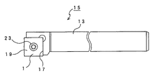
b)次に、本実施例の切削インサート1を装着した工具ユニットについて説明する。
図3に示す様に、前記切削インサート1は、鉄製の柱状のチップホルダ13に、着脱可能に取り付けて使用される。尚、切削インサート1を装着したチップホルダ13を工具ユニット15と称する。
【0028】
具体的には、切削インサート1を、チップホルダ13の先端に設けられた凹状の取付部17に、切削インサート1の外周面が支持されるように嵌め込む。そして、その際に同図の紙面側となった切削インサート1の上面19から、切削インサート1の貫通孔21(図1参照)に固定ネジ23を嵌め込んで、ネジ止めすることにより、切削インサート1をチップホルダ13に固定する。これにより、チップホルダ13に切削インサート1が装着された工具ユニット15が得られる。
【0029】
c)次に、前記切削インサート1の製造方法を説明する。
・まず、基体3の材料である炭化タングステン(WC)粉末とコバルト(Co)粉末とを所定量秤量した後に、湿式にて混合粉砕を行う。
・次に、粉砕した材料に、パラフィンを2重量%添加し、乾燥・造粒を行い、成型用粉末を得る。
【0030】
・次に、得られた粉末を、所定の切削インサート形状に金型成形し、真空中で焼成する。
・次に、この焼成物を研磨して、所定の寸法公差の範囲内の基体3とする。
・次に、この基体3に対して、PVDコーティング、具体的にはアークイオン式物理蒸着法によるコーティングを実施する。
【0031】
・ここで、前記アークイオン式物理蒸着法について説明する。
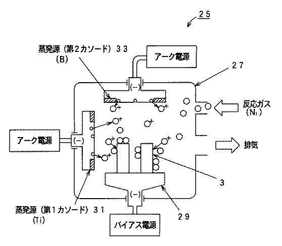
図4に示す様な、アークイオンプレーティング装置(アークイオン式PVD装置)25を用い、その真空チャンバ27内のターンテーブル29上に基体3を配置する。
【0032】
次に、真空チャンバ27内を1.33×10⁻⁴Pa以下まで真空排気した状態で、反応ガス(例えばN2)を供給し、加熱ヒータ(図示せず)によって基体3を加熱する。
そして、高周波電源(図示せず)によって基体3に200Wの出力で電力を供給し、ターンテーブル29を介して基体3にバイアス電源(−)を印加するとともに、被覆膜5のベース層7を構成する金属材料(Ti)を備えた第1蒸発源(第1カソード)31にアーク電源(−)を印加する。
【0033】
これにより、第1カソード31からのTiの金属イオンが、基体3の表面に衝突して蒸着するとともに、供給された反応ガス(N2)が反応し、基体3表面に、TiNのベース層7が形成される。
尚、本実施例では、下記の被覆条件(PVD条件1)で物理蒸着を行うが、その際には、被覆時間(コーティング時間)を調整することにより、被覆膜5の各層の膜厚を調整する。
【0034】
<PVD条件1>
金属材料 :Ti
反応ガス圧 :1.20Pa
基体温度 :500℃
バイアス電圧:−300V
アーク電流 :100A
高周波電源 :200W
・次に、真空チャンバ27内の別の位置(第2カソード)33に配置されたBに対し、第2カソード33に印加するアーク電流値を増加させる方法で制御することにより、その蒸発量を漸近的に増加させる一方、第1カソード31に印加するアーク電流値を減少させる方法で制御することにより、Tiの蒸発量を漸近的に減少させる。これにより、ベース層7の上に、B−Tiの組成が傾斜した中間層9を形成する。
【0035】
尚、被覆条件(PVD条件2)は、下記の通りである。
<PVD条件2>
金属材料 :Ti、B
反応ガス圧 :1.20Pa
基体温度 :500℃
バイアス電圧:−300V
アーク電流 :100A
高周波電源 :200W
・その後、下記PVD条件3により、表面層11を形成する。つまり、Tiの第1カソード31への電圧の印加を止め、基体3に高周波電源より500Wの出力で電力を供給し、−600Vのバイアス電圧を発生させ、Bの第2カソード33のみに電圧を印加し、cBNを含有する所定厚さの表面層11を形成する。
【0036】
<PVD条件3>
金属材料 :B
反応ガス圧 :1.20Pa
基体温度 :500℃
バイアス電圧:−600V
アーク電流 :100〜150A
高周波電源 :500W
尚、cBNの含有量は、Bに印加するアーク電流により制御する。
【0037】
つまり、上述したアークイオン式物理蒸着法により、基体3表面に、順次、ベース層7、中間層9、表面層11を形成して被覆膜5を設け、切削インサート1を完成する。
d)次に、上述した製造方法にて得られた切削インサートの特性を確認した実験例について説明する。
(実験例)
ここでは、上述した製造方法により、下記表1に示す本発明例の試料No.2〜4、6、7、10〜13の切削インサートを製造するとともに、本発明の範囲外の比較例の試料No.1、5、8、9、14の切削インサートを製造した。
【0038】
そして、各試料に対して、被覆膜を構成するベース層、中間層、表面層の厚みを測定した。具体的には、各試料を破断し、その断面の走査型電子顕微鏡(SEM)の写真から、各層の厚みを測定した。その結果を同じく下記表1に記す。
また、各試料の表面層におけるcBNの含有率を求めた。具体的には、X線回折により、cBNの含有率を測定した。その結果を同じく下記表1に記す。
【0039】
更に、各試料を用い、以下の条件で切削性能試験を実施し、その逃げ面摩耗量を測定した。その結果を同じく下記表1に記す。
【0040】
【表1】
【0041】
この表1に示すように、本発明例の試料(請求項1〜4の発明のいずれか)では、被覆膜に剥離が無く、密着性に優れており、また、逃げ面摩耗量が0.25mm以下と小さいので、耐摩耗性に優れており、切削工具として好適である。
それに対して、比較例の試料では、剥離が発生したり、(剥離が無いものでも)逃げ面摩耗量が0.42mm以上と大きいので、密着性が低く、また、耐摩耗性が十分でなく、好ましくない。
【0042】
この様に、本発明の範囲の実施例の切削インサートは、優れた密着性を有し、しかも、cBNによる優れた性能が発揮されるため、切削工具として使用した場合、優れた耐摩耗性を発揮し、安定した加工を長時間にわたり実施することができるという顕著な効果を奏する。
【0043】
尚、本発明は前記実施例になんら限定されるものではなく、本発明の要旨を逸脱しない範囲において種々の態様で実施しうることはいうまでもない。
(1)例えば本発明の切削インサートは、フライス工具やドリル等の他の工具ユニットに適用することができる。
【0044】
尚、本発明の切削インサートと同様な、基体、ベース層、中間層、表面層を備えた構成品は、耐摩耗部品(例えばベアリング、軸受け、セラミックス成形用金型)としても利用できる。
(2)また、前記被覆層は、アークイオン式物理蒸着により形成することが好ましいが、他の周知の方法(例えばARE法等)を採用することも可能である。
【図面の簡単な説明】
【図1】実施例の切削インサートを示す斜視図である。
【図2】実施例の切削インサートの一部破断し拡大して示す断面図である。
【図3】実施例の切削インサートをホルダに取り付けた工具ユニットを示す上面図である。
【図4】アークイオン式PVD装置を示す説明図である。
【符号の説明】
1…切削インサート(切削工具)
3…基体
5…被覆膜
7…ベース層
9…中間膜
11…表面層
13…ホルダ
15…工具ユニット[0001]
TECHNICAL FIELD OF THE INVENTION
The present invention relates to a cutting insert coated with boron nitride having excellent wear resistance, heat resistance, electrical insulation, and thermal conductivity, and a tool unit including the cutting insert. The present invention relates to a cutting insert and a tool unit used for a tool.
[0002]
[Prior art]
BACKGROUND ART Conventionally, cubic boron nitride (hereinafter, also referred to as cBN) has been known to be useful as a heat sink material or a passivation film of an IC because of its excellent electrical insulation and thermal conductivity. .
[0003]
In addition, cBN is a material having the second highest hardness next to diamond, and is more thermally stable than diamond, and has low reactivity with iron, so it is widely used in cutting tools, grinding tools, wear-resistant parts, etc. It is used.
This cBN is artificially synthesized under a high temperature and a high pressure. The synthesis requires an extremely high pressure and temperature of 1700 ° C. or more and 50,000 atm or more, and uses an expensive ultra-high pressure generator. I had to.
[0004]
In addition, what can be formed by an ultra-high pressure device is limited to a small disk-shaped product, and it is extremely difficult to machine into a commonly used cutting tool shape. Therefore, a product in which cBN is brazed to the cutting edge is generally used, but in any case, it is very expensive.
[0005]
Apart from this, in recent years, a method of forming a cBN thin film on a substrate surface under reduced pressure by a gas phase synthesis method has been studied. Although this method has various problems, cBN can be synthesized by physical vapor deposition (PVD) and chemical vapor deposition (CVD).
[0006]
If cBN can be formed on the surface of a cutting tool by the gas phase synthesis method, cBN has excellent features in terms of its hardness, heat resistance, oxidation resistance, coefficient of friction, reactivity with iron, and the like. Therefore, significant improvements in life and performance can be expected.
However, in any of the cBN synthesis methods using the gas phase synthesis method, a cubic phase (Cubic Phase) is formed by the bombardment of excited or accelerated ions. The internal stress is large, and the adhesion to a metal substrate (including a cemented carbide) or a ceramic substrate which is a base of a tool is extremely poor. As a result, the cBN is peeled off from the substrate immediately or within several days after coating.
[0007]
Therefore, for practical use of a cutting tool or the like coated with cBN, it is particularly necessary to improve the bonding strength between the cBN film and the substrate material.
In recent years, the following various methods (1) to (4) have been proposed as countermeasures.
(1) A method in which an intermediate layer is provided between a base and a cBN layer, and the intermediate layer is composed of a Ti layer and a gradient composition layer (of B and N) (see Patent Document 1).
[0008]
(2) A method in which a Ti film and a B-αBN film are provided between the base and the cBN film (see Patent Document 2).
{Circle around (3)} A method of providing a Si layer and a Si 3 N 4 layer between the base and the cBN layer (see Patent Document 3).
[0009]
(4) A method in which a Ti layer, a TiB layer, and a TiBN layer are provided between the base and the cBN layer (see Patent Document 4).
[0010]
[Patent Document 1]
JP-A-3-260054 (page 2, FIG. 1)
[Patent Document 2]
JP-A-4-168263 (page 2, FIG. 1)
[Patent Document 3]
JP-A-3-257154 (page 3)
[Patent Document 4]
JP-A-10-204618 (page 2, FIG. 2)
[0011]
[Problems to be solved by the invention]
However, in the above-mentioned conventional method, the adhesion of the cBN film is still low, which is not sufficient for use as a cutting tool or the like, and further improvement is required. The present invention has been made to solve the above problems, and an object of the present invention is to prevent the surface layer from being peeled off from the substrate in a short period of time after coating the surface layer containing cBN as in the related art. To provide a high cutting insert and tool unit.
[0012]
Means for Solving the Problems and Effects of the Invention
(1) The invention according to claim 1 includes a base, a base layer mainly composed of titanium nitride provided on the surface of the base, an intermediate layer provided on an outer surface of the base layer, and an outer layer of the intermediate layer. A surface layer mainly composed of boron nitride provided on the surface, and in particular, in the present invention, the intermediate layer contains boron, titanium, and nitrogen, and in the surface layer Wherein the ratio of cubic boron nitride to the total boron nitride is 10 to 70 mol%, and the thickness of the surface layer is 0.5 to 1.5 μm.
[0013]
In the present invention, since the base layer is mainly composed of titanium nitride, it has excellent adhesion to the base. Further, since the intermediate layer containing boron, titanium, and nitrogen is disposed between the base layer and the surface layer, the stress generated in the surface layer can be reduced. In particular, in the present invention, since the ratio of cubic boron nitride (cBN) to total boron nitride (BN) in the surface layer is 10 mol% or more, the effect of including cBN, that is, wear resistance, heat resistance, Excellent effects regarding electrical insulation and thermal conductivity can be exhibited. Furthermore, since the ratio of cBN to all BN is 70 mol% or less, the stress of the formed surface layer does not become excessive, and high adhesion can be secured.
[0014]
In addition, in the present invention, since the thickness of the surface layer is 0.5 μm or more and has a sufficient thickness, the effect of cBN, that is, the abrasion resistance, heat resistance, electrical insulation, and thermal conductivity is related. Excellent effect can be demonstrated. Furthermore, since the thickness of the surface layer is 1.5 μm or less, the stress of the formed surface layer does not become excessive, and high adhesion can be secured.
[0015]
As a result, the cutting insert of the present invention does not peel off from the substrate immediately after coating of the surface layer or in a short period of time, such as within several days, as in the related art, and can be put to practical use.
(2) The invention of claim 2 is characterized in that the ratio of cubic boron nitride to total boron nitride in the surface layer is 10 to 50 mol%.
[0016]
The present invention exemplifies a preferred range of the ratio of cBN, and when the ratio of cBN is 50 mol% or less, there is an advantage that the adhesion is higher.
(3) The invention of claim 3 is characterized in that the thickness of the base layer is 0.1 to 0.5 μm.
[0017]
In the present invention, since the thickness of the base layer is 0.1 μm or more, the adhesion to the substrate is high. Further, when the thickness of the base layer is more than 0.5 μm, it is necessary to reduce the thickness of the surface layer or reduce the content of cBN in order to maintain the adhesion of the surface layer. Since no performance can be obtained, the thickness is preferably 0.5 μm or less.
[0018]
(4) The invention according to claim 4, wherein the intermediate layer has a configuration in which the content of the boron asymptotically increases and the content of the titanium asymptotically decreases toward the surface layer. It is characterized by.
The present invention exemplifies the configuration of the intermediate layer, and has a configuration in which the content of boron is asymptotically increased and the content of titanium is asymptotically reduced toward the surface layer, whereby stress relaxation is achieved. Excellent ability.
[0019]
(5) A fifth aspect of the present invention is a tool unit comprising the cutting insert according to any one of the first to fourth aspects, and a holder for holding the cutting insert.
The present invention exemplifies a tool unit in which the above-mentioned cutting insert is attached to a holder.
[0020]
The cutting insert is a tool used for processing a metal material such as cast iron or steel, and is a replaceable tip that is used by being mechanically mounted on a holder or the like.
Among the materials constituting the surface layer and the intermediate layer, examples of the constituent phases other than cBN include hexagonal boron nitride (HBN), wurtzite boron nitride (wBN), and amorphous amorphous BN. Can be
[0021]
Further, examples of the material constituting the base include cemented carbide, ceramics, cermet, and high speed steel.
[0022]
BEST MODE FOR CARRYING OUT THE INVENTION
Hereinafter, an example (example) of an embodiment of a cutting insert and a tool unit of the present invention will be described.
(Example)
a) First, the cutting insert of the present embodiment will be described.
[0023]
As shown in FIG. 1, a cutting insert (cutting tool) 1 of the present embodiment is made of a base material 3 (see FIG. 1) made of a hard material of a cemented carbide (WC-Co-based cemented carbide) equivalent to, for example, JIS K10. 2) is polished into the shape of the ISO standard SNGA120408, and a coating film 5 having a plurality of layer structures is formed on the surface thereof.
[0024]
As shown in FIG. 2 in which the cutting insert 1 is cut away and enlarged, the coating film 5 includes, from the base 3 side, a base layer 7 made of titanium nitride (TiN) provided on the surface of the base, and the base layer 7. An intermediate layer 9 made of titanium (Ti), boron (B), and nitrogen (N) provided on the outer surface of the substrate, and a surface layer 11 made of boron nitride (BN) provided on the outer surface of the intermediate layer 9 It is composed of
[0025]
The thickness of the base layer 7 is in the range of 0.1 to 0.5 μm.
Further, the intermediate layer 9 has a configuration in which the content of B asymptotically increases and the content of Ti asymptotically decreases toward the surface layer 11.
[0026]
Further, the surface layer 11 has a thickness of 0.5 to 1.5 μm, and a ratio of cubic boron nitride (cBN) to all BN in the surface layer 11 is 10 to 70 mol% (preferably 10 to 70 mol%). 50 mol%).
Therefore, the cutting insert 1 of the present embodiment having the above-described configuration can exhibit excellent effects regarding wear resistance, heat resistance, electrical insulation, and thermal conductivity, and has high adhesion of the surface layer 11. There is a feature.
[0027]
b) Next, a tool unit equipped with the cutting insert 1 of the present embodiment will be described.
As shown in FIG. 3, the cutting insert 1 is used by being detachably attached to an iron columnar tip holder 13. Note that the tip holder 13 on which the cutting insert 1 is mounted is referred to as a tool unit 15.
[0028]
Specifically, the cutting insert 1 is fitted into a concave mounting portion 17 provided at the tip of the tip holder 13 so that the outer peripheral surface of the cutting insert 1 is supported. At this time, a fixing screw 23 is fitted into the through hole 21 (see FIG. 1) of the cutting insert 1 from the upper surface 19 of the cutting insert 1 on the paper surface side in FIG. 1 is fixed to the tip holder 13. Thereby, the tool unit 15 in which the cutting insert 1 is mounted on the tip holder 13 is obtained.
[0029]
c) Next, a method for manufacturing the cutting insert 1 will be described.
First, a predetermined amount of tungsten carbide (WC) powder and cobalt (Co) powder, which are materials of the base 3, is weighed and then mixed and pulverized by a wet method.
Next, 2% by weight of paraffin is added to the pulverized material, followed by drying and granulation to obtain a molding powder.
[0030]
Next, the obtained powder is molded into a predetermined cutting insert shape and fired in a vacuum.
Next, the fired product is polished to obtain a substrate 3 within a predetermined dimensional tolerance.
Next, the substrate 3 is subjected to PVD coating, specifically, coating by arc ion physical vapor deposition.
[0031]
Here, the arc ion physical vapor deposition method will be described.
An arc ion plating apparatus (arc ion PVD apparatus) 25 as shown in FIG. 4 is used, and the base 3 is placed on a turntable 29 in a vacuum chamber 27.
[0032]
Next, a reaction gas (for example, N 2 ) is supplied while the inside of the vacuum chamber 27 is evacuated to 1.33 × 10 −4 Pa or less, and the base 3 is heated by a heater (not shown).
Then, power is supplied to the base 3 with an output of 200 W from a high-frequency power supply (not shown), a bias power supply (−) is applied to the base 3 via the turntable 29, and the base layer 7 of the coating film 5 is removed. An arc power supply (-) is applied to a first evaporation source (first cathode) 31 including the constituent metal material (Ti).
[0033]
As a result, the metal ions of Ti from the first cathode 31 collide with the surface of the base 3 and are deposited, and the supplied reaction gas (N 2 ) reacts, so that the base layer 7 of TiN is formed on the surface of the base 3. Is formed.
In this embodiment, physical vapor deposition is performed under the following coating conditions (PVD condition 1). In this case, the coating time (coating time) is adjusted to adjust the film thickness of each layer of the coating film 5. adjust.
[0034]
<PVD condition 1>
Metal material: Ti
Reaction gas pressure: 1.20 Pa
Substrate temperature: 500 ° C
Bias voltage: -300V
Arc current: 100A
High frequency power supply: 200W
Next, the amount of evaporation of B arranged at another position (second cathode) 33 in the vacuum chamber 27 is controlled by increasing the arc current value applied to the second cathode 33. The amount of Ti vaporized is reduced asymptotically by controlling it in such a way as to asymptotically increase the value of the arc current applied to the first cathode 31. Thereby, the intermediate layer 9 in which the composition of B-Ti is inclined is formed on the base layer 7.
[0035]
The coating conditions (PVD condition 2) are as follows.
<PVD condition 2>
Metal material: Ti, B
Reaction gas pressure: 1.20 Pa
Substrate temperature: 500 ° C
Bias voltage: -300V
Arc current: 100A
High frequency power supply: 200W
-Thereafter, the surface layer 11 is formed under the following PVD condition 3. In other words, the application of the voltage of the Ti to the first cathode 31 is stopped, the power is supplied to the base 3 from the high-frequency power supply at an output of 500 W, a bias voltage of −600 V is generated, and the voltage is applied only to the second cathode 33 of the B. This is applied to form a surface layer 11 having a predetermined thickness containing cBN.
[0036]
<PVD condition 3>
Metal material: B
Reaction gas pressure: 1.20 Pa
Substrate temperature: 500 ° C
Bias voltage: -600V
Arc current: 100-150A
High frequency power supply: 500W
The content of cBN is controlled by the arc current applied to B.
[0037]
That is, the base layer 7, the intermediate layer 9, and the surface layer 11 are sequentially formed on the surface of the substrate 3 by the above-described arc ion physical vapor deposition method to provide the coating film 5, and the cutting insert 1 is completed.
d) Next, an experimental example in which the characteristics of the cutting insert obtained by the above-described manufacturing method were confirmed will be described.
(Experimental example)
Here, the sample No. of the present invention example shown in Table 1 below was manufactured by the above-described manufacturing method. Sample Nos. 2 to 4, 6, 7, and 10 to 13 were manufactured, and Sample Nos. Of Comparative Examples outside the scope of the present invention were manufactured. 1, 5, 8, 9, 14 cutting inserts were produced.
[0038]
Then, the thickness of the base layer, the intermediate layer, and the surface layer constituting the coating film was measured for each sample. Specifically, each sample was broken, and the thickness of each layer was measured from a photograph of a cross section of the sample taken with a scanning electron microscope (SEM). The results are also shown in Table 1 below.
The cBN content in the surface layer of each sample was determined. Specifically, the cBN content was measured by X-ray diffraction. The results are also shown in Table 1 below.
[0039]
Further, a cutting performance test was performed on each sample under the following conditions, and the flank wear amount was measured. The results are also shown in Table 1 below.
[0040]
[Table 1]
[0041]
As shown in Table 1, in the sample of the present invention (any one of the inventions of claims 1 to 4), the coating film did not peel off, had excellent adhesion, and had a flank wear amount of 0. Since it is as small as 0.25 mm or less, it has excellent wear resistance and is suitable as a cutting tool.
On the other hand, in the sample of the comparative example, peeling occurs or the flank wear amount (even if there is no peeling) is as large as 0.42 mm or more, so that the adhesion is low and the abrasion resistance is not sufficient. Is not preferred.
[0042]
As described above, the cutting inserts of Examples within the scope of the present invention have excellent adhesion, and also exhibit excellent performance due to cBN. Therefore, when used as a cutting tool, they exhibit excellent wear resistance. It exerts a remarkable effect that it is possible to perform stable processing for a long time.
[0043]
It should be noted that the present invention is not limited to the above-described embodiment at all, and it goes without saying that the present invention can be implemented in various modes without departing from the gist of the present invention.
(1) For example, the cutting insert of the present invention can be applied to other tool units such as a milling tool and a drill.
[0044]
In addition, the component provided with the base, the base layer, the intermediate layer, and the surface layer similar to the cutting insert of the present invention can also be used as a wear-resistant part (for example, a bearing, a bearing, a ceramic molding die).
(2) Further, the coating layer is preferably formed by arc ion physical vapor deposition, but other well-known methods (for example, the ARE method) can also be adopted.
[Brief description of the drawings]
FIG. 1 is a perspective view showing a cutting insert according to an embodiment.
FIG. 2 is a cross-sectional view showing a cutting insert of an embodiment in a partially broken and enlarged view.
FIG. 3 is a top view showing a tool unit in which the cutting insert of the embodiment is mounted on a holder.
FIG. 4 is an explanatory view showing an arc ion type PVD apparatus.
[Explanation of symbols]
1. Cutting insert (cutting tool)
3 ... Base 5 ... Coating film 7 ... Base layer 9 ... Intermediate film 11 ... Surface layer 13 ... Holder 15 ... Tool unit