JP2004319476A - Polymer switch and manufacturing method of polymer switch - Google Patents
Polymer switch and manufacturing method of polymer switch Download PDFInfo
- Publication number
- JP2004319476A JP2004319476A JP2004112425A JP2004112425A JP2004319476A JP 2004319476 A JP2004319476 A JP 2004319476A JP 2004112425 A JP2004112425 A JP 2004112425A JP 2004112425 A JP2004112425 A JP 2004112425A JP 2004319476 A JP2004319476 A JP 2004319476A
- Authority
- JP
- Japan
- Prior art keywords
- switch
- heater
- liquid metal
- polymer
- channel
- Prior art date
- Legal status (The legal status is an assumption and is not a legal conclusion. Google has not performed a legal analysis and makes no representation as to the accuracy of the status listed.)
- Pending
Links
Images

Classifications
-
- H—ELECTRICITY
- H01—ELECTRIC ELEMENTS
- H01H—ELECTRIC SWITCHES; RELAYS; SELECTORS; EMERGENCY PROTECTIVE DEVICES
- H01H29/00—Switches having at least one liquid contact
- H01H29/28—Switches having at least one liquid contact with level of surface of contact liquid displaced by fluid pressure
-
- H—ELECTRICITY
- H01—ELECTRIC ELEMENTS
- H01H—ELECTRIC SWITCHES; RELAYS; SELECTORS; EMERGENCY PROTECTIVE DEVICES
- H01H11/00—Apparatus or processes specially adapted for the manufacture of electric switches
- H01H11/02—Apparatus or processes specially adapted for the manufacture of electric switches for mercury switches
-
- H—ELECTRICITY
- H01—ELECTRIC ELEMENTS
- H01H—ELECTRIC SWITCHES; RELAYS; SELECTORS; EMERGENCY PROTECTIVE DEVICES
- H01H1/00—Contacts
- H01H1/0036—Switches making use of microelectromechanical systems [MEMS]
-
- H—ELECTRICITY
- H01—ELECTRIC ELEMENTS
- H01H—ELECTRIC SWITCHES; RELAYS; SELECTORS; EMERGENCY PROTECTIVE DEVICES
- H01H29/00—Switches having at least one liquid contact
- H01H2029/008—Switches having at least one liquid contact using micromechanics, e.g. micromechanical liquid contact switches or [LIMMS]
Abstract
Description
本発明は光学スイッチング用の超小型電気機械システム(MEMS)に関するものであり、より具体的にはポリマー液体金属スイッチ(以下「ポリマー・スイッチ」とも称する。)に関する。 The present invention relates to micro-electromechanical systems (MEMS) for optical switching, and more particularly to polymer liquid metal switches (hereinafter also referred to as "polymer switches").
気体の加熱を利用して気圧変化を作ることにより、チャネル内に閉じ込めた液体金属の液滴間に(電気コンタクトを開くように)ギャップを作り、また、これらの液滴を(電気コンタクトを閉じるように)移動させてコンタクト間を濡らすことによりスイッチを作動させる液体金属スイッチはこれまでにも考案されている。チャネル構造を製造する為に用いられる現在の方法は、サンドブラスト法を使用してチャネルを形成することから、その分解能及び精度に限界があった。加えて、現在、ヒーター抵抗器はセラミック基板上に形成されている為、熱がセラミック基板へと失われ、エネルギー効率が悪いものである。
したがって、本発明の目的は、ポリマー層を導入して高精度かつエネルギー効率の高い液体金属スイッチを提供することにある。 Accordingly, it is an object of the present invention to provide a highly accurate and energy efficient liquid metal switch by introducing a polymer layer.
本発明は、スイッチング・チャネルがポリマー層内に形成されたポリマー・スイッチに関する。チャネルの形成は、レーザーアブレーション或いはフォトイメージング等のマイクロマシン技術により形成することが出来る。液体金属スイッチは、スイッチング・チャネル内に含まれている。この液体金属スイッチは、液体金属塊を用いて電気コンタクトを形成したり、これを切断したりすることにより作動する。スイッチング・チャネル内のコンタクト・パッドは液体金属に対する濡れ性を持っており、スイッチのラッチング機構を提供するものである。スイッチはマイクロマシン加工により小型に製作することが可能である。 The present invention relates to a polymer switch in which the switching channel is formed in a polymer layer. The channel can be formed by micromachine technology such as laser ablation or photoimaging. A liquid metal switch is included within the switching channel. The liquid metal switch operates by making and breaking electrical contacts using a liquid metal mass. The contact pads in the switching channels are wettable to the liquid metal and provide a latching mechanism for the switch. The switch can be manufactured small by micromachining.
新規性を持つと考えられる本発明の特徴は、具体的に請求項に記載した。しかしながら本発明自体は、添付図を参照しつつ特定の実施例を説明する以下の本発明の詳細な説明を読むことにより、その目的及び利点と共に構成及び作動方法を最も良く理解することが出来る。 The features of the invention believed to be novel are set forth with particularity in the appended claims. However, the invention itself, together with its objects and advantages, will best be understood by reference to the following detailed description of the invention which, when read in conjunction with the accompanying drawings, illustrates certain embodiments.
本発明は多くの異なる形態の実施例に適用することが可能であるが、本願においては図に示した1つ以上の特定の実施例に沿って説明する。しかしながら、本開示はあくまでも本発明の原理の一例にしか過ぎず、本発明を図示及び説明する特定の実施例に制約する意図はない。以下の説明においては、同じ参照数字、符号が複数の図にわたり、同一、同様又は対応する部分を示す為に用いられている。 Although the present invention is applicable to many different embodiments, the present application will be described with reference to one or more specific embodiments shown in the figures. However, this disclosure is merely an example of the principles of the present invention and is not intended to be limited to the particular embodiments illustrated and described. In the following description, the same reference numerals and symbols are used to indicate the same, similar, or corresponding parts in a plurality of drawings.
本発明の一側面は、ポリイミド又はその他のポリマー・フィルム即ちポリマー層のレーザーアブレーションといった、液体金属スイッチにおけるチャネル構造製作におけるマイクロマシン加工技術の利用方法である。この方法は、サンドブラスト法によるものよりも良好な許容差及び分解能を提供するものである。一実施例においては、チャネル層はカプトン(Kapton;商標)(ポリイミドのシート形態のもの)又は他の好適なポリマー・フィルムにレーザーアブレーション法により必要なチャネル造作を形成することで作られる。その後チャネル層は、サイトップ(Cytop;商標)又はカプトンKJ(KJ;商標;接着特性を持つ熱可塑性ポリイミド)のような好適な接着剤を用いてスイッチ基板へと接着される。カプトンは水蒸気に対する透湿性を持っている。完成した組み立て部品から水蒸気を排除しておく必要がある場合、組み立て部品を気密封止パッケージングするか、或いは不浸水性の支持板に重ねてはんだによりスイッチ基板へと封止することにより「自己パッケージング」させることが出来る。この支持板は、例えば、金属、ガラス、シリコン或いはセラミックとすることが出来る。 One aspect of the present invention is the use of micromachining techniques in channel structure fabrication in liquid metal switches, such as laser ablation of polyimide or other polymer films or polymer layers. This method provides better tolerances and resolution than the sandblast method. In one embodiment, the channel layer is made by forming the required channel features by laser ablation on Kapton ™ (in the form of a sheet of polyimide) or other suitable polymer film. Thereafter, the channel layer is adhered to the switch substrate using a suitable adhesive such as Cytop (trademark) or Kapton KJ (thermoplastic polyimide having adhesive properties). Kapton is permeable to water vapor. If water vapor needs to be excluded from the completed assembly, the assembly can be hermetically sealed or packaged, or placed on a non-water impregnated support plate and soldered to the switch substrate for sealing. Packaging. " This support plate can be, for example, metal, glass, silicon or ceramic.
更なる実施例においては、支持板に好適な液体ポリマー(スピンオン・ポリイミド等)を塗布して硬化させ、その後レーザーアブレーションにより所望のチャネル構造を作ることによりポリマー・チャネル層を製作することが出来る。代わりに、材料がフォトイメージング可能なものである場合、材料を硬化させる前に必要なフィーチャを露光及び現像することによりチャネル構造を作ることが出来る。完成したチャネル層はスピンコート又はスプレイコート法により形成された後に例えばフォトイメージング又はレーザーアブレーションされた接着剤の層を含むものであっても良い。サイトップは前者の方法により、KJは後者の方法により処理することが出来る。 In a further embodiment, a polymer channel layer can be fabricated by applying and curing a suitable liquid polymer (such as spin-on polyimide) on a support plate and then creating the desired channel structure by laser ablation. Alternatively, if the material is photoimageable, the channel structure can be created by exposing and developing the required features before curing the material. The completed channel layer may include a layer of adhesive that has been formed by spin coating or spray coating, for example, photo-imaging or laser ablated. Cytop can be processed by the former method, and KJ can be processed by the latter method.
また、抵抗器から基板への熱の損失は出来る限り避けることが望ましい。これは、抵抗器を設ける前に、スイッチ基板の表面にポケットを設け、これらをポリイミド等の低熱伝導性ポリマーで満たすことにより可能となる。抵抗器への駆動信号は、例えばスイッチ基板を貫通するバイア又はスイッチ基板上面又は中を通るトレースにより伝えることが出来る。 It is also desirable to minimize the heat loss from the resistor to the substrate. This is made possible by providing pockets on the surface of the switch substrate before filling the resistors and filling them with a low thermal conductivity polymer such as polyimide. Drive signals to the resistors can be conveyed, for example, by vias through the switch substrate or traces through or through the switch substrate.
更に他の実施例においては、スイッチ基板に低熱伝導率と高温耐性を持つポリイミド等のポリマーを用いることにより抵抗器から基板への熱の損失を小さくすることが出来る。抵抗器は、所望によりポリイミド上へと直接的に、或いは中間層上に設けることが出来る。ヒーター領域の下及び近傍のポリイミドを薄くすることにより、ヒーター領域の熱伝導率及び熱容量を小さくすることが出来る。しかしながらこの手法においては、気密性が求められる場合に別個のパッケージを必要とするという欠点がある。 In still another embodiment, the loss of heat from the resistor to the substrate can be reduced by using a polymer such as polyimide having low thermal conductivity and high temperature resistance for the switch substrate. The resistor can be provided directly on the polyimide or on the interlayer if desired. By reducing the thickness of the polyimide under and near the heater region, the thermal conductivity and heat capacity of the heater region can be reduced. However, this approach has the disadvantage of requiring a separate package when tightness is required.
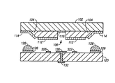
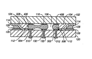
図1は自己パッケージングされた本発明の一実施例に基づくポリマー液体金属スイッチの断面図である。図1に示したスイッチは最終組み立て工程前の、2つの部品として描かれている。上部部品は、ポリマー層104を覆うチャネル支持板102を含んでいる。チャネル支持板102は例えばセラミック又はシリコンから作ることが出来る。ポリマーは、例えば不活性プラスチックで高温耐性を持つポリイミドとすることが出来る。スイッチング・チャネル106はポリマー層内に形成される。接着剤の層112はポリマー層104の下側を覆っている。接着剤は、例えばサイトップ又はKJとすることが出来る。接着剤は代わりに下部部品のスイッチ基板120の上面に塗布しても良い。一実施例においては、接着剤層は約7μm厚である。上部はんだリング114はチャネル支持板102の下面外周及びポリマー層104の側面に取り付けられる。上部はんだリングは溶融はんだに対する濡れ性を持っている。
FIG. 1 is a cross-sectional view of a self-packaged polymer liquid metal switch according to one embodiment of the present invention. The switch shown in FIG. 1 is depicted as two parts before the final assembly process. The upper part includes a
図1に示したスイッチの下部部品は、透明スイッチ基板120を含んでいる。基板は例えばセラミックから作ることが出来る。下部はんだリング126はスイッチ基板120の内面側の外周に設けられている。下部はんだリングは溶融はんだ128に対する濡れ性を持つ。符号130に示したような濡れ性コンタクト・パッドもまた、スイッチ基板120の内面上に形成されており、上下2つの部品が組み立てられた場合にスイッチの上部部品内にあるチャネル106と位置が合うことになる。濡れ性コンタクト・パッド130は水銀等の液体金属に対する濡れ性を持っているが、この液体金属はスイッチ内のラッチング機構を提供する為に用いられるものである。本実施例においては、このコンタクト・パッドは約800nm厚である。コンタクト・パッド130は、スイッチ基板120内のバイアを通じてスイッチ基板の下側にあるはんだパッド132と接続している。更に他の実施例においては、コンタクト・パッドはスイッチ基板の上面上に設けられたトレースを通じて回路基板の端部へと接続している。オプションとして、符号116で示したような追加コンタクト・パッドをチャネル支持板102へと設けることが出来る。電気配線306及び322はヒーターへと結合しているが、ヒーターについては後に説明する。
The lower part of the switch shown in FIG. 1 includes a
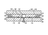
図2は、組み立てられたスイッチの断面図である。接着剤層112はポリマー層104をスイッチ基板120へと接着しており、スイッチ内に空洞106が作られている。濡れ性を持つコンタクト・パッド130は空洞106の一方の側に配置されている。はんだ128は表面張力により引っ張られて上部はんだリング114と下部はんだリング126間のギャップを埋めている。これによりスイッチ内部に高い信頼性を持つ気密封止が提供されることになる。充分なはんだが設けられている限りにおいては、濡れ性を持つはんだリングにより、封止が確実に完全なものとなるのである。
FIG. 2 is a sectional view of the assembled switch. An
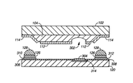
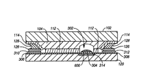
図3は本発明のポリマー・スイッチの他の断面図である。上部部品内のポリマー層104はヒーター空洞302を含んでいる。抵抗器等のヒーター304はスイッチ基板120の内側面上に配置されており、このヒーター空洞302と整列している。2つの部品が組み立てられた場合、ヒーターはヒーター空洞の内部に配置される。電気配線306及び308はヒーターへの電気接続を提供する。動作中は、電圧がヒーターに印加され、ヒーター空洞内にある気体が加熱され、これにより気体の圧力及び体積が増大する。絶縁層310及び312は、電気配線306及び308とはんだリング126間の電気的絶縁性を提供している。これらの層は、例えばスピンオン・ガラス、或いはSiNx又はSiO2のような薄膜パッシベーション層とすることが出来る。これらの層は、はんだリング間のはんだ接合形成を妨げないように充分薄くすることが望ましい。ポリマー層314(ポリイミド層等)はヒーター304をスイッチ基板120から分離しており、基板への熱の損失を低減している。
FIG. 3 is another cross-sectional view of the polymer switch of the present invention.
図4はチャネル支持板102の下面を示す図である。上部はんだリング114はチャネル支持板102の内側表面の外周に設けられている。チャネル402はポリマー層104内にある。この図においては、接着剤112は図示していない。チャネル内にあるのは、ヒーター空洞302及び404と、スイッチング・チャネル106である。スイッチング・チャネル106内には、3つのコンタクト・パッド406、116及び408がある。コンタクト・パッドの表面は液体金属に対する濡れ性を持つ。オプションとして、スイッチ基板120上のコンタクト・パッドへと電気接続を作るかわりに、1つ以上のこれらのコンタクト・パッドへと電気接続を作ることも出来る。1−1断面は、図1における上部部品の断面である。3−3断面は、90°回転させて図3の上部部品として示した。5−5断面は、90°回転させて図5の上部部品として示した。
FIG. 4 is a diagram illustrating the lower surface of the
図5は、組み立てられたポリマー・スイッチを、図4にいて5−5切断した断面図である。スイッチング・チャネル106内には、上部コンタクト・パッド406、116及び408と対応する下部コンタクト・パッド502、130及び504がある。上部及び下部コンタクト・パッドはコンタクト・リングを形成するように結合させることが出来る。スイッチング・チャネル内に更にあるのは、2つの液体金属塊506及び508として示した液体金属塊である。液体金属塊は液体金属の表面張力によってコンタクト・パッドと接触して支持されている。濡れ性のコンタクト・パッド及び液体金属の表面張力により、スイッチのラッチング機構が提供されている。図5に示したように液体金属が分布している場合、コンタクト・パッド130及び504間には電気接続が作られているが、一方でコンタクト・パッド130及び502間には接続がない。ヒーター(図3における304)に電圧が印加されると、ヒーター空洞(図3における302)内の気圧が上昇する。ヒーター空洞はスイッチング・チャネル106と結合している為、図5におけるスイッチング・チャネルの右端における気圧もまた上昇することになる。上昇した気圧は表面張力を上回り、コンタクト・パッド408及び504間、及びコンタクト・パッド116及び130間の液体金属結合を壊す。液体金属の一部はスイッチング・チャネル106に沿って移動し、液体金属塊508と合体する。このように、コンタクト・パッド130及び504間(又は116及び408間)の電気接続は切断される一方で、コンタクト・パッド130及び502間(又は116及び406間)に接続が形成されることになる。この結果得られたスイッチ状態を図6に示す。電圧がヒーター空洞404(図4)内の対応するヒーターに印加された場合、スイッチ状態は逆転することになる。
FIG. 5 is a cross-sectional view of the assembled polymer switch taken along a line 5-5 in FIG. Within the switching
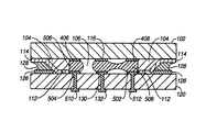
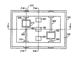
図7はスイッチの下部部分の内側表面(例えばスイッチ基板120の上面)を示すものである。下部はんだリング126はスイッチ基板120の外周を覆っている。はんだ自体は図示していない。ヒーター304は、スイッチが組み立てられるとヒーター空洞302(図3及び図4に図示)と整列するように基板上に配置されている。ヒーター702は、スイッチが組み立てられるとヒーター空洞404(図4に図示)と整列するように基板上に配置されている。電気接続306及び308はヒーター304から基板端部まで延びており、これによりヒーターへ電圧を印加することが出来る。かわりに、ヒーター接続はスイッチ基板内のバイアを通じたものであっても良い。絶縁層310及び312はヒーター接続をはんだリング126から絶縁する。ポリマー層314はヒーター304をスイッチ基板120から分離するものである。対応する接続(320及び322)及び絶縁層が、第2のヒーター702を基板端部まで接続する為に用いられる。コンタクト・パッド502、130及び504は、スイッチング・チャネル内の液体金属に濡れる表面を持っている。線1−1に沿う断面は、図1における下部部品として示した部分である。線3−3に沿う断面は、90°回転させて図3の下部部品として示した。線5−5に沿う断面は、90°回転させて図5の下部部品として示した。
FIG. 7 illustrates the inside surface of the lower portion of the switch (eg, the top surface of switch substrate 120). The
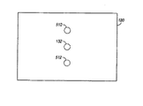
図8は、スイッチ基板120の外部表面を示す図である。はんだパッド又は電気コネクタ510、132及び512は、回路基板内のバイアを通じて信号をスイッチへと接続することが出来る。他の実施例においては、チャネル支持板の外部表面上にこの電気コネクタが1つ以上設けられる。更に他の実施例においては、コネクタはスイッチの端部に設けられ、回路基板内に設けられた導電路を通じてコンタクト・パッドへと結合される。
FIG. 8 is a diagram illustrating an external surface of the
図9は本発明のポリマー・スイッチの他の断面図を示す。ポリマー層104はヒーター空洞302を含んでいる。抵抗器等のヒーター304はスイッチ基板120の内側表面にあるヒーター空洞302内に配置される。相転移液体600はヒーターと濡れ接触している。電気配線306及び308はヒーターへの電気接続を提供する。作動においては、電圧がヒーターへと印加され、相転移液体600が液体状態から気体状態へと変化する。これに付随する体積増加により気圧が上昇し、上述したようにスイッチが起動することになる。ヒーターが冷めると、相転移液体600はヒーター304の表面上へと凝縮する。第2のヒーター空洞(図4の304)内には対応する相転移液体が含まれている。この相転移液体は、例えば不活性無機質液体、或いは液体金属とすることが出来る。
FIG. 9 shows another cross-sectional view of the polymer switch of the present invention.
本発明を特定の実施例に沿って説明してきたが、上述の説明に照らして多数の代替、変更、入れ替え及び改変が可能であることは、当業者であれば明らかである。従って、本発明はそのような代替、変更、入れ替え及び改変形態を全て請求項の範囲に入るものとして包含することを意図したものである。なお、本発明の実施態様の一部を下記して本発明の実施の参考に供する。なお、本発明の理解を容易にするために実施例での参照番号を付記した。 Although the present invention has been described in terms of particular embodiments, it is evident to those skilled in the art that many alternatives, changes, permutations, and modifications are possible in light of the above description. Accordingly, the invention is intended to embrace all such alternatives, changes, permutations and modifications as fall within the scope of the appended claims. A part of the embodiments of the present invention will be described below for reference of the practice of the present invention. It should be noted that reference numerals in the examples have been added to facilitate understanding of the present invention.
(実施態様1):スイッチ基板(120)と、チャネル支持板(102)と、前記チャネル支持板(102)と前記スイッチ基板(120)との間に固定されたポリマー層(104)と、前記ポリマー層(104)内に形成されたスイッチング・チャネル(106)と、第1及び第2の電気コネクタ(510、132)と、前記スイッチング・チャネル(106)内に備えられ、前記第1及び第2の電気コネクタ(510、132)間で電気回路を形成または切断する液体金属スイッチとを具備したポリマー・スイッチ。 (Embodiment 1): a switch substrate (120), a channel support plate (102), a polymer layer (104) fixed between the channel support plate (102) and the switch substrate (120), A switching channel (106) formed in a polymer layer (104); first and second electrical connectors (510, 132); and a first and second electrical connector provided in the switching channel (106). A liquid metal switch for forming or cutting an electrical circuit between the two electrical connectors (510, 132).
(実施態様2):前記チャネル支持板と前記スイッチ基板との間に更に気密封止を具備し、前記気密封止(128)、前記チャネル支持板(102)及び前記スイッチ基板(120)が前記ポリマー層(104)を包囲していることを特徴とし、前記気密封止が、前記チャネル支持板(102)の内側表面外周に取り付けられ、前記ポリマー層(104)を取り囲む、溶融はんだに濡れる第1のはんだリング(114)と、前記スイッチ基板(120)の内側表面外周に取り付けられた、溶融はんだに濡れる第2のはんだリング(126)と、前記第1、第2のはんだリングを接続するはんだ接合(128)とを有することを特徴とする実施態様1に記載のポリマー・スイッチ。 (Embodiment 2): further comprising a hermetic seal between the channel support plate and the switch substrate, wherein the hermetic seal (128), the channel support plate (102) and the switch substrate (120) are Surrounding the polymer layer (104), wherein the hermetic seal is attached to the outer periphery of the inner surface of the channel support plate (102) and surrounds the polymer layer (104) and is wetted by molten solder. A first solder ring (114), a second solder ring (126) attached to the outer peripheral surface of the inside of the switch substrate (120) and wetted by molten solder, and the first and second solder rings are connected. 2. The polymer switch according to claim 1, comprising a solder joint (128).
(実施態様3):前記液体金属スイッチが、(1)前記スイッチング・チャネル(106)内に位置し、前記第1の電気コネクタ(510)へと電気的に接続し、液体金属に濡れる表面を持つ第1の外部コンタクト・パッド(502)と、(2)前記スイッチング・チャネル(106)内に位置し、液体金属に濡れる表面を持つ第2の外部コンタクト・パッド(504)と、(3)前記第1、第2の外部コンタクト・パッド(502、504)の間の前記スイッチング・チャネル(106)内に位置し、前記第2の電気コネクタ(132)へ電気的に接続し、液体金属に濡れる表面を持つ中間コンタクト・パッド(130)と、(4)前記スイッチング・チャネル(106)内に備えられ、前記第1の外部コンタクト・パッド(502)と濡れ接触する第1の液体金属塊(508)と、(5)前記スイッチング・チャネル(106)内に備えられ、前記第2の外部コンタクト・パッド(504)と濡れ接触する第2の液体金属塊(506)と、(6)前記スイッチング・チャネル(106)内に備えられ、前記中間コンタクト・パッド(130)と濡れ接触する第3の液体金属塊とを具備し、(7)前記第3の液体金属塊が、前記第1、第2の液体金属塊(508、506)のいずれか一方に合体するように構成されていることを特徴とする実施態様1に記載のポリマー・スイッチ。 (Embodiment 3): The liquid metal switch is (1) located in the switching channel (106), electrically connected to the first electrical connector (510), and having a liquid metal wet surface. A first external contact pad (502) having (2) a second external contact pad (504) located within said switching channel (106) and having a liquid metal wettable surface; (3) Located in the switching channel (106) between the first and second external contact pads (502, 504), and electrically connected to the second electrical connector (132), and connected to the liquid metal. An intermediate contact pad (130) having a wettable surface; and (4) wetted with the first external contact pad (502) provided in the switching channel (106). A first liquid metal mass (508) in contact with; and (5) a second liquid metal mass (50) provided in the switching channel (106) and in wet contact with the second external contact pad (504). 506) and (6) a third liquid metal mass provided in the switching channel (106) and in wet contact with the intermediate contact pad (130); (7) the third liquid 2. The polymer switch of embodiment 1, wherein a metal mass is configured to coalesce with one of the first and second liquid metal masses (508, 506).
(実施態様4):前記液体金属スイッチが、(1)前記ポリマー層(104)内に形成され、前記スイッチング・チャネル(106)に結合する第1のヒーター空洞(302)と、(2)前記ポリマー層(104)内に形成され、前記スイッチング・チャネル(106)に結合する第2のヒーター空洞(404)と、(3)前記第1のヒーター空洞(302)内に配置され、前記第1の空洞内の流体を加熱するように適合した第1のヒーター(304)と、前記第2のヒーター空洞(404)内に配置され、前記第2の空洞内の流体を加熱するように適合した第2のヒーター(702)とを更に具備し、前記第1のヒーター(304)の作動により、前記第3の液体金属塊が第1の液体金属塊(508)と合体し、前記第2のヒーター(702)の作動により、前記第3の液体金属塊が第2の液体金属塊(506)と合体することを特徴とする実施態様3に記載のポリマー・スイッチ。
(Embodiment 4): The liquid metal switch comprises: (1) a first heater cavity (302) formed in the polymer layer (104) and coupled to the switching channel (106); A second heater cavity (404) formed in the polymer layer (104) and coupled to the switching channel (106); and (3) disposed in the first heater cavity (302) and the first heater cavity (302). A first heater (304) adapted to heat the fluid in the second cavity; and a first heater (304) disposed in the second heater cavity (404) and adapted to heat the fluid in the second cavity. A second heater (702), wherein the operation of the first heater (304) causes the third liquid metal lump to merge with the first liquid metal lump (508); Heater (70 By the operation of) the polymer switch of
(実施態様5):前記第1、第2のヒーター(304、702)の少なくとも一方が、低熱伝導率を持つパッド(314)により前記スイッチ基板から分離されていることを特徴とする実施態様4に記載のポリマー・スイッチ。 (Embodiment 5): Embodiment 4 characterized in that at least one of the first and second heaters (304, 702) is separated from the switch substrate by a pad (314) having a low thermal conductivity. A polymer switch according to claim 1.
(実施態様6):前記第1、第2の外部コンタクト・パッド(502、504)及び前記中間コンタクト・パッド(130)のうちの少なくとも1つが、一方が前記チャネル支持板(102)の内側表面に固定され、他方が前記スイッチ基板(120)の内側表面に固定された一対のコンタクト・パッド(502及び406、504及び408、或いは130及び116)、或いは前記スイッチング・チャネル(106)の壁に取り付けられたコンタクト・リングのいずれかを具備したものであることを特徴とする実施態様3に記載のポリマー・スイッチ。
Embodiment 6: At least one of the first and second external contact pads (502, 504) and the intermediate contact pad (130), one of which is an inner surface of the channel support plate (102). And a pair of contact pads (502 and 406, 504 and 408, or 130 and 116) fixed to the inside surface of the switch substrate (120) or the walls of the switching channel (106). 4. The polymer switch of
(実施態様7):前記第2の外部コンタクト・パッド(504)に結合する第3の電気コネクタ(512)を更に具備し、前記液体金属スイッチが、更に前記第2、第3の電気コネクタ(132、512)間の電気回路を形成又は切断するように作動するものであることを特徴とする実施態様3に記載のポリマー・スイッチ。 (Embodiment 7) The apparatus further comprises a third electrical connector (512) coupled to the second external contact pad (504), wherein the liquid metal switch further comprises the second and third electrical connectors (512). 132, 512), wherein the polymer switch is operable to form or break an electrical circuit between them.
(実施態様8):ポリマー・スイッチの製造方法であって、(イ)スイッチ基板(120)上に複数の電気コンタクト・パッド(502、130、504)を形成するステップと、(ロ)前記スイッチ基板(120)上にヒーター(304)を形成するステップと、(ハ)ポリマー層(104)内に、スイッチング・チャネル(106)及び前記スイッチング・チャネル(106)に結合するヒーター空洞(302)を有するチャネル構造(402)を形成するステップと、(ニ)前記コンタクト・パッド(502、130、504)の少なくとも1つの上に液体金属塊(506、508)を配置するステップと、(ホ)前記ヒーター(304)が前記ヒーター空洞(302)内に入り、前記複数のコンタクト・パッド(502、130、504)が前記スイッチング・チャネル(106)内に入るように、前記スイッチ基板(120)を前記ポリマー層(104)へと取り付けるステップとを有するポリマー・スイッチの製造方法。 Embodiment 8: A method of manufacturing a polymer switch, comprising: (a) forming a plurality of electrical contact pads (502, 130, 504) on a switch substrate (120); and (b) the switch. Forming a heater (304) on the substrate (120); and (c) forming a switching channel (106) and a heater cavity (302) coupled to the switching channel (106) in the polymer layer (104). (D) forming a liquid metal mass (506, 508) on at least one of the contact pads (502, 130, 504); A heater (304) enters the heater cavity (302) and receives the plurality of contact pads (502, 130, 5). 4) As enters the switching channel (106) within the method for producing a polymer-switch and a step of attaching the said switch substrate (120) to the polymer layer (104).
(実施態様9):前記ポリマー層(104)内の前記チャネル構造(402)が、マイクロマシン加工により形成されることを特徴とする実施態様8に記載のポリマー・スイッチの製造方法。 Embodiment 9: The method for manufacturing a polymer switch according to embodiment 8, wherein the channel structure (402) in the polymer layer (104) is formed by micromachining.
(実施態様10):(ヘ)溶融はんだに対する濡れ性を持つ第1のはんだリング(114)を前記チャネル支持板(102)の内側表面の外周へと取り付けるステップと、(ト)溶融はんだに濡れる第2のはんだリング(126)をスイッチ基板(120)の内側表面の外周へと取り付けるステップと、(チ)前記第1のはんだリング(114)を前記第2のはんだリング(126)へはんだ付けし、前記ポリマー層(104)の周囲に封止(128)を形成するステップを更に有する実施態様8に記載のポリマー・スイッチの製造方法。 (Embodiment 10): (f) attaching a first solder ring (114) having wettability to molten solder to the outer periphery of the inner surface of the channel support plate (102); Attaching a second solder ring (126) to the outer periphery of the inside surface of the switch substrate (120); and (h) soldering the first solder ring (114) to the second solder ring (126). 9. The method of claim 8, further comprising forming a seal (128) around the polymer layer (104).
102 チャネル支持板
104 ポリマー層
106 スイッチング・チャネル
114 第1のはんだリング
126 第2のはんだリング
128 気密封止(はんだ接合部)
130 中間コンタクト・パッド
132 第2の電気コネクタ
302 第1のヒーター空洞
304 第1のヒーター
314 低熱伝導率を持つパッド、ポリマー層
402 チャネル構造
404 第2のヒーター空洞
502 第1の外部コンタクト・パッド
504 第2の外部コンタクト・パッド
506 第2の液体金属塊
508 第1の液体金属塊
510 第1の電気コネクタ
512 第3の電気コネクタ
702 第2のヒーター
102
130
Claims (1)
チャネル支持板と、
前記チャネル支持板と前記スイッチ基板との間に固定されたポリマー層と、
前記ポリマー層内に形成されたスイッチング・チャネルと、
第1、第2の電気コネクタと、
前記スイッチング・チャネル内に備えられ、前記第1、第2の電気コネクタ間の電気回路を形成、或いは切断する液体金属スイッチと、
を具備したポリマー・スイッチ。 A switch board,
A channel support plate;
A polymer layer fixed between the channel support plate and the switch substrate;
A switching channel formed in the polymer layer;
First and second electrical connectors;
A liquid metal switch provided in the switching channel for forming or disconnecting an electrical circuit between the first and second electrical connectors;
A polymer switch comprising:
Applications Claiming Priority (1)
| Application Number | Priority Date | Filing Date | Title |
|---|---|---|---|
| US10/413,094 US6743991B1 (en) | 2003-04-14 | 2003-04-14 | Polymeric liquid metal switch |
Publications (2)
| Publication Number | Publication Date |
|---|---|
| JP2004319476A true JP2004319476A (en) | 2004-11-11 |
| JP2004319476A5 JP2004319476A5 (en) | 2007-04-05 |
Family
ID=32298258
Family Applications (1)
| Application Number | Title | Priority Date | Filing Date |
|---|---|---|---|
| JP2004112425A Pending JP2004319476A (en) | 2003-04-14 | 2004-04-06 | Polymer switch and manufacturing method of polymer switch |
Country Status (5)
| Country | Link |
|---|---|
| US (1) | US6743991B1 (en) |
| JP (1) | JP2004319476A (en) |
| DE (1) | DE10360994A1 (en) |
| GB (1) | GB2400735B (en) |
| TW (1) | TW200425197A (en) |
Cited By (1)
| Publication number | Priority date | Publication date | Assignee | Title |
|---|---|---|---|---|
| JP2007042636A (en) * | 2005-08-01 | 2007-02-15 | Avago Technologies Ecbu Ip (Singapore) Pte Ltd | Fluid switch, and method of manufacturing the same |
Families Citing this family (18)
| Publication number | Priority date | Publication date | Assignee | Title |
|---|---|---|---|---|
| JP2004079288A (en) * | 2002-08-13 | 2004-03-11 | Agilent Technol Inc | Electrical contact switching device using liquid metal |
| US6888977B2 (en) * | 2003-04-14 | 2005-05-03 | Agilent Technologies, Inc. | Polymeric liquid metal optical switch |
| US6798937B1 (en) * | 2003-04-14 | 2004-09-28 | Agilent Technologies, Inc. | Pressure actuated solid slug optical latching relay |
| US7189934B2 (en) * | 2003-11-13 | 2007-03-13 | Honeywell International Inc. | Self-healing liquid contact switch |
| US6822176B1 (en) * | 2004-04-16 | 2004-11-23 | Agilent Technologies, Inc. | Liquid metal switch and method of manufacture therefor |
| US7164090B2 (en) * | 2005-02-28 | 2007-01-16 | Agilent Technologies, Inc. | Liquid metal switch employing a single volume of liquid metal |
| US20060211233A1 (en) * | 2005-03-21 | 2006-09-21 | Skyworks Solutions, Inc. | Method for fabricating a wafer level package having through wafer vias for external package connectivity and related structure |
| US7576426B2 (en) * | 2005-04-01 | 2009-08-18 | Skyworks Solutions, Inc. | Wafer level package including a device wafer integrated with a passive component |
| US20060289607A1 (en) * | 2005-06-28 | 2006-12-28 | Buchwalter Stephen L | Composite solder transfer moldplate structure and method of making same |
| US7358452B2 (en) * | 2005-06-30 | 2008-04-15 | Agilent Technlolgies, Inc. | Architecture and method of fabrication for a liquid metal microswitch (LIMMS) |
| US7358833B2 (en) * | 2006-03-14 | 2008-04-15 | Lucent Technologies Inc. | Method and apparatus for signal processing using electrowetting |
| US7449649B2 (en) * | 2006-05-23 | 2008-11-11 | Lucent Technologies Inc. | Liquid switch |
| US7635606B2 (en) * | 2006-08-02 | 2009-12-22 | Skyworks Solutions, Inc. | Wafer level package with cavities for active devices |
| US20080217708A1 (en) * | 2007-03-09 | 2008-09-11 | Skyworks Solutions, Inc. | Integrated passive cap in a system-in-package |
| US20090001576A1 (en) * | 2007-06-29 | 2009-01-01 | Surinder Tuli | Interconnect using liquid metal |
| KR20100115735A (en) | 2007-11-30 | 2010-10-28 | 스카이워크스 솔루션즈, 인코포레이티드 | Wafer level packaging using flip chip mounting |
| US8900931B2 (en) * | 2007-12-26 | 2014-12-02 | Skyworks Solutions, Inc. | In-situ cavity integrated circuit package |
| US7939945B2 (en) | 2008-04-30 | 2011-05-10 | Intel Corporation | Electrically conductive fluid interconnects for integrated circuit devices |
Family Cites Families (5)
| Publication number | Priority date | Publication date | Assignee | Title |
|---|---|---|---|---|
| KR0174871B1 (en) | 1995-12-13 | 1999-02-01 | 양승택 | Thermally driven micro relay device with latching characteristics |
| US6323447B1 (en) | 1998-12-30 | 2001-11-27 | Agilent Technologies, Inc. | Electrical contact breaker switch, integrated electrical contact breaker switch, and electrical contact switching method |
| US6373356B1 (en) | 1999-05-21 | 2002-04-16 | Interscience, Inc. | Microelectromechanical liquid metal current carrying system, apparatus and method |
| US6512322B1 (en) | 2001-10-31 | 2003-01-28 | Agilent Technologies, Inc. | Longitudinal piezoelectric latching relay |
| US6515404B1 (en) | 2002-02-14 | 2003-02-04 | Agilent Technologies, Inc. | Bending piezoelectrically actuated liquid metal switch |
-
2003
- 2003-04-14 US US10/413,094 patent/US6743991B1/en not_active Expired - Fee Related
- 2003-10-28 TW TW092129941A patent/TW200425197A/en unknown
- 2003-12-23 DE DE10360994A patent/DE10360994A1/en not_active Withdrawn
-
2004
- 2004-03-30 GB GB0407165A patent/GB2400735B/en not_active Expired - Fee Related
- 2004-04-06 JP JP2004112425A patent/JP2004319476A/en active Pending
Cited By (2)
| Publication number | Priority date | Publication date | Assignee | Title |
|---|---|---|---|---|
| JP2007042636A (en) * | 2005-08-01 | 2007-02-15 | Avago Technologies Ecbu Ip (Singapore) Pte Ltd | Fluid switch, and method of manufacturing the same |
| JP4701136B2 (en) * | 2005-08-01 | 2011-06-15 | アバゴ・テクノロジーズ・イーシービーユー・アイピー(シンガポール)プライベート・リミテッド | Fluid switch and manufacturing method thereof |
Also Published As
| Publication number | Publication date |
|---|---|
| GB0407165D0 (en) | 2004-05-05 |
| US6743991B1 (en) | 2004-06-01 |
| GB2400735A (en) | 2004-10-20 |
| DE10360994A1 (en) | 2004-11-25 |
| TW200425197A (en) | 2004-11-16 |
| GB2400735B (en) | 2006-05-24 |
Similar Documents
| Publication | Publication Date | Title |
|---|---|---|
| JP2004319476A (en) | Polymer switch and manufacturing method of polymer switch | |
| CA2637414C (en) | Miniaturized high conductivity thermal/electrical switch | |
| KR20090038379A (en) | Sealed wafer packaging of microelectromechanical systems | |
| JP2011175893A (en) | Resistance temperature fuse package and resistance temperature fuse | |
| JP2004319476A5 (en) | ||
| US6806431B2 (en) | Liquid metal micro-relay with suspended heaters and multilayer wiring | |
| JP2004318136A (en) | Polymer optical switch and method of manufacturing the same | |
| JP2004342598A (en) | Electric relay array | |
| JP2004335456A (en) | Electric switching assembly | |
| JP2004319477A (en) | Structure for electric switch and switching method | |
| US7137412B2 (en) | Relay | |
| JP2009224387A (en) | Semiconductor device and method of manufacturing the same | |
| JP2004319501A (en) | Electric relay | |
| SE533459C2 (en) | Method of encapsulating solar cells | |
| JP4964505B2 (en) | Semiconductor device, manufacturing method thereof, and electronic component | |
| JP2004318136A5 (en) | ||
| JP2004319488A (en) | Electric relay | |
| JP2004319497A (en) | High-frequency liquid metal latching relay having plane contact | |
| JP2005158717A (en) | Fluid-based switch and method for manufacturing and sealing fluid-based switch | |
| EP1391903A1 (en) | Micro-relay device | |
| TW200421638A (en) | Latching relay with switch bar | |
| JP5349024B2 (en) | Optical device and method of manufacturing optical device | |
| JP2004193133A (en) | Switch, and assembling method for switch | |
| JP2004319481A (en) | Electric relay array | |
| JP2004319479A (en) | High-frequency inflection type latching relay |
Legal Events
| Date | Code | Title | Description |
|---|---|---|---|
| A521 | Request for written amendment filed |
Free format text: JAPANESE INTERMEDIATE CODE: A523 Effective date: 20070216 |
|
| A621 | Written request for application examination |
Free format text: JAPANESE INTERMEDIATE CODE: A621 Effective date: 20070216 |
|
| RD02 | Notification of acceptance of power of attorney |
Free format text: JAPANESE INTERMEDIATE CODE: A7422 Effective date: 20070508 |
|
| RD04 | Notification of resignation of power of attorney |
Free format text: JAPANESE INTERMEDIATE CODE: A7424 Effective date: 20070514 |
|
| A131 | Notification of reasons for refusal |
Free format text: JAPANESE INTERMEDIATE CODE: A131 Effective date: 20090821 |
|
| A02 | Decision of refusal |
Free format text: JAPANESE INTERMEDIATE CODE: A02 Effective date: 20100202 |