JP2004319477A - Structure for electric switch and switching method - Google Patents
Structure for electric switch and switching method Download PDFInfo
- Publication number
- JP2004319477A JP2004319477A JP2004112465A JP2004112465A JP2004319477A JP 2004319477 A JP2004319477 A JP 2004319477A JP 2004112465 A JP2004112465 A JP 2004112465A JP 2004112465 A JP2004112465 A JP 2004112465A JP 2004319477 A JP2004319477 A JP 2004319477A
- Authority
- JP
- Japan
- Prior art keywords
- liquid metal
- switch
- coupled
- layer
- contacts
- Prior art date
- Legal status (The legal status is an assumption and is not a legal conclusion. Google has not performed a legal analysis and makes no representation as to the accuracy of the status listed.)
- Pending
Links
Images


Classifications
-
- H—ELECTRICITY
- H01—ELECTRIC ELEMENTS
- H01H—ELECTRIC SWITCHES; RELAYS; SELECTORS; EMERGENCY PROTECTIVE DEVICES
- H01H57/00—Electrostrictive relays; Piezo-electric relays
-
- H—ELECTRICITY
- H01—ELECTRIC ELEMENTS
- H01H—ELECTRIC SWITCHES; RELAYS; SELECTORS; EMERGENCY PROTECTIVE DEVICES
- H01H29/00—Switches having at least one liquid contact
- H01H29/28—Switches having at least one liquid contact with level of surface of contact liquid displaced by fluid pressure
-
- H—ELECTRICITY
- H01—ELECTRIC ELEMENTS
- H01H—ELECTRIC SWITCHES; RELAYS; SELECTORS; EMERGENCY PROTECTIVE DEVICES
- H01H29/00—Switches having at least one liquid contact
- H01H2029/008—Switches having at least one liquid contact using micromechanics, e.g. micromechanical liquid contact switches or [LIMMS]
-
- H—ELECTRICITY
- H01—ELECTRIC ELEMENTS
- H01H—ELECTRIC SWITCHES; RELAYS; SELECTORS; EMERGENCY PROTECTIVE DEVICES
- H01H57/00—Electrostrictive relays; Piezo-electric relays
- H01H2057/006—Micromechanical piezoelectric relay
Abstract
Description
本発明は、概して電子装置及びシステムの分野に関し、更に詳しくは、電気、電子スイッチング技術に関するものである。 The present invention relates generally to the field of electronic devices and systems, and more particularly to electrical and electronic switching technology.
リレイやスイッチを使用することにより、電気信号を第1状態から第2状態に変化させることができる。一般的には、2状態より多い。小型スイッチや小さな領域内に多数のスイッチを必要とする用例では、超小型電子部品製造法を使用し、占有面積の小さなスイッチを製造することができる。半導体スイッチは、産業機器、通信機器、及びインクジェットプリンタのような電子機械装置の制御などの様々な用例で使用可能である。 By using a relay or a switch, the electric signal can be changed from the first state to the second state. Generally, there are more than two states. In applications requiring small switches or a large number of switches in a small area, a microelectronic component manufacturing method can be used to produce a switch with a small footprint. Semiconductor switches can be used in various applications, such as industrial equipment, communication equipment, and control of electromechanical devices such as inkjet printers.
スイッチング用例では、圧電技術を使用してスイッチを作動させることができる。圧電材料は、いくつかの固有の特徴を有しており、印加電圧に応答して圧電材料を伸張又は短縮させることができる。これは、間接的圧電効果と呼ばれるものである。この伸張又は短縮の量、伸張又は短縮によって生成される力、及び連続的な短縮間の時間間隔は、特定の用例における圧電材料の適用法に影響を与える重要な材料特性である。又、圧電材料は、直接的な圧電効果をも有しており、これは、印加した力に応答して電界を生成する現象である。圧電材料にコンタクトを適切に接続すれば、この電界を電圧に変換することができる。間接的圧電効果は、スイッチング素子内においてコンタクトを形成又は切断するのに有用であり、直接的圧電効果は、印加した力に応答してスイッチング信号を生成するのに有用である。
本発明の目的は、圧電駆動による液体金属スイッチ、特に押し出し素子を備えるスイッチの提供にある。 It is an object of the present invention to provide a piezoelectrically driven liquid metal switch, in particular a switch with a push-out element.
電気スイッチ用の構造及びスイッチング方法を開示する。本発明の構造によれば、液体充填チャンバが固体材料内に収容されている。液体充填チャンバ内のスイッチ・コンタクトが固体材料に結合しており、圧電素子が複数の薄膜に結合している。複数の薄膜は、液体充填チャンバに結合している。そして、複数のスイッチ・コンタクトが複数の液体金属小滴に結合している。本発明の方法によれば、圧電素子を作動させ、薄膜素子を偏向させる。この薄膜素子の偏向により、駆動流体である駆動液体の圧力が上昇し、この駆動液体の圧力の上昇により、電気スイッチの第1コンタクトと第2コンタクト間における液体金属の接続が切断される。 A structure and a switching method for an electrical switch are disclosed. According to the structure of the invention, the liquid filling chamber is contained in a solid material. A switch contact in the liquid-filled chamber is bonded to a solid material, and the piezoelectric element is bonded to a plurality of thin films. A plurality of membranes are coupled to the liquid filling chamber. A plurality of switch contacts are coupled to the plurality of liquid metal droplets. According to the method of the present invention, the piezoelectric element is actuated to deflect the thin-film element. Due to the deflection of the thin film element, the pressure of the driving liquid, which is the driving fluid, increases, and the connection of the liquid metal between the first contact and the second contact of the electric switch is cut off due to the increase in the pressure of the driving liquid.
新規性を有すると考えられる本発明の特徴については、添付の特許請求の範囲に具体的に記述されている。しかしながら、以下の添付図面との関連で、本発明の特定の模範的な実施例について記述する本明細書の本発明に関する詳細な説明を参照することにより、本発明の目的及び効果、並びに、その構成及び動作方法の両方の観点から、本発明自体について十分に理解することができよう。 The features of the invention believed to be novel are set forth with particularity in the appended claims. However, by reference to the detailed description of the invention herein which describes particular exemplary embodiments of the invention in connection with the accompanying drawings, the objects and advantages of the invention, and its The invention itself can be fully understood from both a configuration and a method of operation.
本発明によれば、多数の異なる態様の実施例が可能であり、図面及び本明細書においては、特定の実施例について図示並びに詳述しているが、この開示内容は、本発明の原理の一例と見なすべきであって、図示及び説明するこれら特定の実施例に本発明を限定することを意図するものではない。尚、以下の説明においては、同じ参照符号を使用し、添付図面のいくつかの図において同一、類似、又は対応する部分を示している。 While many different embodiments of the invention are possible in accordance with the present invention and which are shown and described in detail in the drawings and specification, the disclosure is not to be construed as limiting the principles of the invention. It should be considered as an example, and is not intended to limit the invention to these particular embodiments shown and described. In the following description, the same reference numerals are used, and the same, similar, or corresponding parts are shown in some of the accompanying drawings.
液体金属スイッチは、複数の層を使用して表現することが可能であり、これら複数の層は、液体金属スイッチの製造の際に生成される層を表している。 The liquid metal switch can be represented using a plurality of layers, which represent the layers created during the manufacture of the liquid metal switch.
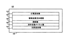
まず、図1を参照すれば、本発明の特定の実施例による押し出し式液体金属スイッチ105の側面図100が示されている。この押し出し式液体金属スイッチ105は、複数の別個の層から構成可能であり、これら複数の層は、複数の機能を提供している。圧電基板層110は、駆動装置流体槽層120に結合している。この駆動装置流体槽層120は、薄膜層130に結合しており、薄膜層130は、液体金属チャネル層140に結合している。そして、液体金属チャネル層140は、回路基板層150に更に結合している。尚、回路基板層150は、複数の回路トレースを更に有することが可能であり、図1には、これら複数の回路トレースが示されていないことに留意されたい。又、図1に示されている1つ又は複数の層は、本発明の精神と範囲を逸脱することなく、組み合わせて別の名称を付与することも可能であることに留意されたい。一例として、薄膜とチャネルを有するチャネル層として、薄膜層130と液体金属チャネル層140を組み合わせることが可能である。又、本発明の精神と範囲を逸脱することなく、1つ又は複数の更なる層を設けることも可能であることに留意されたい。本発明の特定の実施例においては、これらの圧電基板層110、駆動装置流体槽層120、薄膜層130、液体金属チャネル層140、及び回路基板層150は、ガラス、セラミック、複合材料、及びセラミック被覆材料の1つ又は複数のから構成可能である。
Referring first to FIG. 1, there is shown a
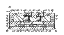
次に図2を参照すれば、本発明の特定の実施例による押し出し式液体金属スイッチ105の断面図200が示されている。この断面図200は、複数のコンタクト210に結合する圧電基板層110を示しており、これら複数のコンタクト210は、複数のビア225に結合している。この複数のビア225により、対応する複数の圧電素子215に電位を印加することができる。電位は、複数のコンタクト210の中の2つのコンタクトを使用して印加可能である。これらの2つのコンタクトは、複数の絶縁体220の1つによって絶縁されている。図2に示されているように、この複数の絶縁体220のそれぞれは、複数のコンタクト210のそれぞれのコンタクト対に結合している。本発明の特定の実施例においては、複数の絶縁体220、複数の圧電素子215、及び複数のコンタクト210のそれぞれのコンタクトのセグメントは、駆動装置流体槽層120内に配置されている。本発明の特定の実施例においては、押し出し素子227は、複数の圧電素子215の中の1つの圧電素子、複数の絶縁体220の中の1つの絶縁体、複数のコンタクト210の中の1対のコンタクトのセグメントから構成されている。
Referring now to FIG. 2, there is shown a
押し出し素子227は、駆動装置流体槽層120内に存在している。押し出し素子227は、隣接する押し出し素子から駆動流体205によって分離されている。本発明の特定の実施例においては、駆動装置流体槽層120内のそれぞれの押し出し素子は、駆動流体205によって分離されている。本発明の特定の実施例においては、駆動流体205は、「3M フロリナート(商標)」などの、不活性であって、粘度が低く、沸点の高い流体から構成されている。正の電位は、複数の圧電素子215の中の1つの圧電素子を伸長させるように作用し、負の電位は、複数の圧電素子215の中の1つの圧電素子を短縮させるように作用させることができる。尚、本発明の精神と範囲を逸脱することなく、正の電位を使用して圧電素子を短縮させ、負の電位を使用して圧電素子を伸長させることも可能であることに留意されたい。図2に示されているように、押し出し素子227は、薄膜層130に結合しており、この結果、押し出し素子227の伸長により、薄膜層130が押圧され、これにより、スイッチング流体230が薄膜層130から液体金属チャネル層140のチャネル240内に伸張することになる。
The
チャネル240は、複数の液体金属235、複数のスイッチ・コンタクト245、及びスイッチング流体230を有している。水銀やガリウム合金などの液体金属235は、摩擦軽減潤滑材として機能する。複数の液体金属235は、複数のスイッチ・コンタクト245に結合しており、複数の液体金属235の中の1つは、複数のスイッチ・コンタクト245の中の2つに結合している。これらの複数のスイッチ・コンタクト245は、回路基板層150に更に結合している。
Channel 240 has a plurality of
押し出し式液体金属スイッチ105は、複数のコンタクト210の中の2つに電位を印加することによって動作する。この印加電位により、複数の圧電素子の中の1つが伸長する。この伸長により、スイッチング流体230の圧力が上昇する。この結果、スイッチング流体230がチャンバ240内に押しやられる。チャンバ240における対応するスイッチング流体230の圧力上昇により、複数の液体金属235の中で現在複数のスイッチ・コンタクト245の中の第1スイッチ・コンタクトと第2スイッチ・コンタクトに結合している1つの液体金属が、2つの別個の領域に分離する。そして、この2つの別個の領域の中の第1の領域は、第1のスイッチ・コンタクトに結合しており、第2の領域は、第2のスイッチ・コンタクトに結合している。本発明の特定の実施例においては、液体金属は、第2領域が複数のスイッチ・コンタクト245の中の第2スイッチ・コンタクトと第3スイッチ・コンタクトに結合するように分離する。この複数の液体金属235の中の1つの液体金属の分離は、押し出し式液体金属スイッチ105の値を第1状態から第2状態に変化させるべく動作可能である。尚、本発明の特定の実施例においては、この液体金属の分離は、第3スイッチ・コンタクトを使用することなしに押し出し式液体金属スイッチ105の状態を変化させるのに使用するよう動作可能である。液体金属は、液体金属と第2スイッチ・コンタクト及び第3スイッチ・コンタクトの対応する表面間の表面張力により、第2スイッチ・コンタクト及び第3スイッチ・コンタクトに結合した状態に維持される。
The push-out
又、第1押し出し素子により、第1スイッチ・コンタクト及び第2スイッチ・コンタクトに結合した複数の液体金属235の中の1つの液体金属を分離させ、液体金属が第2スイッチ・コンタクト及び第3スイッチ・コンタクトに結合するように、2つの押し出し素子を使用することも可能であることに留意されたい。次いで、第2押し出し素子を使用し、第2スイッチ・コンタクト及び第3スイッチ・コンタクトに結合している液体金属を分離することができる。本発明の特定の実施例においては、第1押し出し素子に押し出し(プッシュ;伸長)させると共に、第2押し出し素子に引っ込み(プル;短縮)させ、この結果、第1押し出し素子によって液体金属が押圧されると同時に、第2押し出し素子が液体金属を引き離す負圧を生成するようにすることができる。
Also, the first push element separates one of the plurality of
次に図3を参照すれば、本発明の特定の実施例による押し出し式液体金属スイッチ105の回路基板層110の第1平面図300が示されている。この第1平面図300は、複数のコンタクト210の配列を示している。尚、これら複数のコンタクト210は、正方形の上部形状を有するものとして示されているが、本発明の精神と範囲を逸脱することなく、円形などのその他の形状を使用することも可能である。
Referring now to FIG. 3, there is shown a
次に図4を参照すれば、本発明の特定の実施例による押し出し式液体金属スイッチ105の液体金属チャネル層140の平面図400が示されている。この平面図400は、複数の貫通孔405を示すチャネル240の平面図415を示しており、複数の貫通孔405は、スイッチング流体230が強力にチャネル240内に進入することを可能にするべく作用する。これらの複数の貫通孔405は、スイッチング流体230の圧力が上昇し、この結果、複数の液体金属235の中の1つの液体金属の分離が良好に行われるようなサイズになっている。又、液体金属チャネル層140の断面図410もあわせて示されている。この断面図410は、チャネル240の幅に対する複数の貫通孔405の幅を示している。尚、図4には2つの貫通孔が示されているが、本発明の精神と範囲を逸脱することなく、更に多くの数の貫通孔を使用することも可能であることに留意されたい。又、複数の貫通孔405は、複数の別個の幅を有するように実施可能であることにも留意されたい。これら複数の別個の幅は、スイッチング流体230の量と複数の圧電素子215の伸長又は短縮の量に整合するように選択可能である。
Referring now to FIG. 4, a
次に図5を参照すれば、本発明の特定の実施例による押し出し式液体金属スイッチ105の薄膜層130の平面図500が示されている。この平面図500は、流体流制限部510の図を含む薄膜層130の向きを示している。流体流制限部510は、駆動装置流体槽層120内に流入するスイッチング流体230の量を制御するべく作用可能である。流体流制限部510は、十分な圧力が複数の液体金属235の中の1つの液体金属に伝達されると共に、十分な量のスイッチング流体230が提供されるようなサイズになっている。あわせて示す薄膜層130の断面図505は、複数の薄膜515に対する流体流制限部510の配置を示している。
Referring now to FIG. 5, a
次に図6を参照すれば、本発明の特定の実施例による押し出し式液体金属スイッチ105の駆動装置流体槽層120の平面図600が示されている。この平面図600は、駆動流体230を格納する槽610のサイズを示している。あわせて示す駆動装置流体槽層120の断面図605には、槽610の幾何学形状が更に示されている。
Referring now to FIG. 6, a
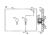
次に図7を参照すれば、本発明の特定の実施例による押し出し式液体金属スイッチ105の圧電基板層110の底面図700が示されている。この底面図700は、複数の駆動装置227の配置を示している。断面図705には、複数のコンタクト210の中の1つのコンタクトの配置が更に示されている。又、図7には、注入口710も示されている。注入口710は、槽610に駆動流体205を充填するのに使用するべく実施可能である。本発明の特定の実施例においては、駆動流体205は、押し出し式液体金属スイッチ105の組み立ての際に充填され、その後、注入口710は密閉される。
Referring now to FIG. 7, a
以上、特定の実施例との関連で本発明について説明したが、当業者には、以上の説明から、多数の代替、変更、置換、変形が明らかになるであろうことが明白である。従って、本発明は、添付の特許請求の範囲に属するそれらの代替、変更、及び変形をも包含するものである。なお、本発明の実施態様の一部を下記して本発明の実施の参考に供する。なお、本発明の理解を容易にするために実施例での参照番号を付記した。 While the present invention has been described in relation to particular embodiments, it is evident to those skilled in the art that numerous alternatives, modifications, substitutions, and variations will be apparent from the foregoing description. Accordingly, the invention is intended to cover such alternatives, modifications and variations as fall within the scope of the appended claims. A part of the embodiments of the present invention will be described below for reference of the practice of the present invention. It should be noted that reference numerals in the examples have been added to facilitate understanding of the present invention.
(実施態様1):電気スイッチ(105)用の構造において、固体材料(130、140、150)内に収容され、駆動液体(230)が充填されたチャンバ(240)と、前記チャンバ内で前記固体材料に結合している複数のスイッチ・コンタクト(245)と、前記複数のスイッチ・コンタクトと前記チャンバとに結合した複数の液体金属小滴(235)と、前記チャンバに結合した複数の薄膜(515)に結合する複数の圧電素子(215)と、を有する電気スイッチ用構造。 (Embodiment 1): In a structure for an electric switch (105), a chamber (240) housed in a solid material (130, 140, 150) and filled with a driving liquid (230); A plurality of switch contacts coupled to a solid material; a plurality of liquid metal droplets coupled to the plurality of switch contacts and the chamber; and a plurality of thin films coupled to the chamber. And 515) coupled to the piezoelectric element (215).
(実施態様2):前記複数の薄膜は、対応する複数の開口部(510)に結合しており、前記複数の開口部の1つは、前記駆動液体の流速を増大させるべく動作可能なことを特徴とする実施態様1に記載の電気スイッチ用構造。 (Embodiment 2): The plurality of thin films are coupled to a corresponding plurality of openings (510), and one of the plurality of openings is operable to increase a flow rate of the driving liquid. 2. The structure for an electric switch according to embodiment 1, wherein
(実施態様3):電気スイッチ(105)用の構造において、圧電基板層(110)と、前記圧電基板層に結合し、1つ又は複数の圧電駆動型押し出し素子(227)を有する駆動装置流体槽層(120)と、前記駆動装置流体槽層に結合し、前記1つ又は複数の圧電駆動型押し出し素子に結合する1つ又は複数の薄膜(515)を有する薄膜層(130)と、
前記薄膜層に結合する液体金属チャネル層(140)と、前記液体金属チャネル層に結合する回路基板層(150)と、前記液体金属チャネル層内に収容され、1つ又は複数のスイッチ・コンタクト(245)に結合する1つ又は複数の液体金属小滴(235)を有し、前記1つ又は複数の薄膜に結合している駆動液体充填チャンバ(240)と、を有することを特徴とする電気スイッチ用構造。
(Embodiment 3): In a structure for an electric switch (105), a driving fluid having a piezoelectric substrate layer (110) and one or more piezoelectric driven extrusion elements (227) coupled to the piezoelectric substrate layer. A tank layer (120); a thin film layer (130) having one or more thin films (515) coupled to the driver fluid tank layer and coupled to the one or more piezoelectrically driven extrusion elements;
A liquid metal channel layer coupled to the thin film layer; a circuit board layer coupled to the liquid metal channel layer; and one or more switch contacts contained within the liquid metal channel layer. 245) having one or more liquid metal droplets (235) coupled thereto, and a driving liquid filling chamber (240) coupled to said one or more thin films. Structure for switch.
(実施態様4):前記駆動装置流体槽層、圧電基板層、薄膜層、回路基板層、及び液体金属チャネル層は、ガラス、セラミック、複合材料、及びセミラック被覆材料の1つ又は複数から構成可能であることを特徴とする実施態様3に記載の電気スイッチ用構造。 (Embodiment 4): The driving device fluid bath layer, the piezoelectric substrate layer, the thin film layer, the circuit board layer, and the liquid metal channel layer can be composed of one or more of glass, ceramic, composite material, and semi-rack coating material. 4. The structure for an electric switch according to embodiment 3, wherein
(実施態様5):前記駆動装置流体槽層は、該駆動装置流体槽層の槽(610)への駆動流体の充填に使用するべく動作可能な注入口(710)を更に有することを特徴とする実施態様3に記載の電気スイッチ用構造。 (Embodiment 5): The driving device fluid reservoir layer further includes an inlet (710) operable to be used to fill a driving fluid into the reservoir (610) of the driving device fluid reservoir layer. 4. The structure for an electric switch according to claim 3, wherein
(実施態様6):前記回路基板層は、前記1つ又は複数の圧電駆動型押し出し素子の中の1つ又は複数の作動によって生成された1つ又は複数の信号をルーティングするべく動作可能な複数の回路トレースと複数のパッドを更に有することを特徴とする実施態様3に記載の電気スイッチ用構造。 Embodiment 6: The circuit board layer is operable to route one or more signals generated by one or more actuations of the one or more piezoelectrically driven extrusion elements. 3. The structure for an electrical switch according to claim 3, further comprising a circuit trace and a plurality of pads.
(実施態様7):液体金属スイッチ(105)を使用して1つ又は複数の電気信号を電気的にスイッチングする方法において、圧電素子(215)を作動させる段階と、前記圧電素子の作動によって薄膜素子(515)を偏向させる段階と、前記薄膜素子の偏向によって駆動液体(230)の圧力を上昇させる段階と、前記駆動液体の圧力の上昇により、前記液体金属スイッチの第1コンタクト(245)と第2コンタクト(245)間の液体金属(235)による接続を切断する段階と、を有するスイッチング方法。 Embodiment 7: A method of electrically switching one or more electrical signals using a liquid metal switch (105), wherein actuating a piezoelectric element (215) and actuating the piezoelectric element to form a thin film. Deflecting the element (515), increasing the pressure of the driving liquid (230) by deflecting the thin-film element, and increasing the pressure of the driving liquid to contact the first contact (245) of the liquid metal switch. Disconnecting the liquid metal (235) connection between the second contacts (245).
(実施態様8):前記圧電素子は、該圧電素子の第1側部と、該第1側部の反対側に位置する第2側部と、に印加される電位の印加によって作動することを特徴とする実施態様7に記載のスイッチング方法。 (Embodiment 8): The piezoelectric element operates by applying an electric potential applied to a first side of the piezoelectric element and a second side opposite to the first side. A switching method according to claim 7, wherein the switching method is characterized in that:
(実施態様9):前記液体金属による接続は、液体金属(235)と前記第1コンタクト及び前記第2コンタクト間の表面張力によって維持されることを特徴とする実施態様7に記載のスイッチング方法。 (Embodiment 9): The switching method according to embodiment 7, wherein the connection by the liquid metal is maintained by surface tension between the liquid metal (235) and the first contact and the second contact.
(実施態様10):開口部(510)を使用し、前記圧力の上昇によって発生する駆動液体の流速を増大させ、前記増大した流速が、前記液体金属による接続をより迅速に切断するべく動作可能であることを特徴とする実施態様7に記載のスイッチング方法。 (Embodiment 10): The opening (510) is used to increase the flow rate of the driving liquid generated by the increase in the pressure, and the increased flow rate is operable to disconnect the liquid metal connection more quickly. The switching method according to embodiment 7, wherein:
105 液体金属スイッチ,電気スイッチ
110 圧電基板層
120 駆動装置流体槽層
130 薄膜層
140 液体金属チャネル層
150 回路基板層
215 圧電素子
227 圧電駆動型押し出し素子
230 駆動液体
235 液体金属小滴
240 駆動液体充填チャンバ
245 スイッチ・コンタクト
510 開口部、流体流制限部
515 薄膜
610 槽
710 注入口
Claims (1)
固体材料内に収容され、駆動液体が充填されたチャンバと、
前記チャンバ内で前記固体材料に結合している複数のスイッチ・コンタクトと、
前記複数のスイッチ・コンタクトと前記チャンバとに結合した複数の液体金属小滴と、
前記チャンバに結合した複数の薄膜に結合する複数の圧電素子と、
を有する電気スイッチ用構造。 In a structure for an electric switch,
A chamber housed in a solid material and filled with a driving liquid;
A plurality of switch contacts coupled to the solid material in the chamber;
A plurality of liquid metal droplets coupled to the plurality of switch contacts and the chamber;
A plurality of piezoelectric elements coupled to a plurality of thin films coupled to the chamber;
A structure for an electric switch, comprising:
Applications Claiming Priority (1)
| Application Number | Priority Date | Filing Date | Title |
|---|---|---|---|
| US10/413,098 US7012354B2 (en) | 2003-04-14 | 2003-04-14 | Method and structure for a pusher-mode piezoelectrically actuated liquid metal switch |
Publications (2)
| Publication Number | Publication Date |
|---|---|
| JP2004319477A true JP2004319477A (en) | 2004-11-11 |
| JP2004319477A5 JP2004319477A5 (en) | 2007-04-05 |
Family
ID=32298259
Family Applications (1)
| Application Number | Title | Priority Date | Filing Date |
|---|---|---|---|
| JP2004112465A Pending JP2004319477A (en) | 2003-04-14 | 2004-04-06 | Structure for electric switch and switching method |
Country Status (5)
| Country | Link |
|---|---|
| US (1) | US7012354B2 (en) |
| JP (1) | JP2004319477A (en) |
| DE (1) | DE10359279A1 (en) |
| GB (1) | GB2400747B (en) |
| TW (1) | TW200421381A (en) |
Families Citing this family (10)
| Publication number | Priority date | Publication date | Assignee | Title |
|---|---|---|---|---|
| US6946775B2 (en) * | 2003-04-14 | 2005-09-20 | Agilent Technologies, Inc. | Method and structure for a slug assisted longitudinal piezoelectrically actuated liquid metal optical switch |
| US7012354B2 (en) * | 2003-04-14 | 2006-03-14 | Agilent Technologies, Inc. | Method and structure for a pusher-mode piezoelectrically actuated liquid metal switch |
| US6876130B2 (en) * | 2003-04-14 | 2005-04-05 | Agilent Technologies, Inc. | Damped longitudinal mode latching relay |
| US20080150659A1 (en) * | 2005-08-31 | 2008-06-26 | Matsushita Electric Works, Ltd. | Relay Device Using Conductive Fluid |
| KR101092536B1 (en) * | 2005-11-30 | 2011-12-13 | 삼성전자주식회사 | Piezoelectric RF MEMS Device and the Method for Producing the Same |
| US20070289853A1 (en) * | 2006-06-14 | 2007-12-20 | Timothy Beerling | Tailoring of switch bubble formation for LIMMS devices |
| DE102007035020A1 (en) * | 2007-07-26 | 2009-01-29 | Qimonda Ag | Contact device for use in chip test arrangement, for contacting electrical contact, has opening through which electrically conductive liquid produces contact for electrical contact |
| EP2416313B1 (en) * | 2010-08-05 | 2013-11-06 | BlackBerry Limited | Electronic device including actuator for providing tactile output |
| US8855705B2 (en) | 2010-08-05 | 2014-10-07 | Blackberry Limited | Electronic device including actuator for providing tactile output |
| US8914075B2 (en) | 2010-09-17 | 2014-12-16 | Blackberry Limited | Electronic device including actuator and method of controlling same for providing tactile output |
Family Cites Families (87)
| Publication number | Priority date | Publication date | Assignee | Title |
|---|---|---|---|---|
| US2312672A (en) * | 1941-05-09 | 1943-03-02 | Bell Telephone Labor Inc | Switching device |
| US2564081A (en) * | 1946-05-23 | 1951-08-14 | Babson Bros Co | Mercury switch |
| GB1143822A (en) * | 1965-08-20 | |||
| DE1614671B2 (en) * | 1967-12-04 | 1971-09-30 | Siemens AG, 1000 Berlin u. 8000 München | INDEPENDENT MERCURY RELAY |
| US3639165A (en) * | 1968-06-20 | 1972-02-01 | Gen Electric | Resistor thin films formed by low-pressure deposition of molybdenum and tungsten |
| US3600537A (en) * | 1969-04-15 | 1971-08-17 | Mechanical Enterprises Inc | Switch |
| US3657647A (en) * | 1970-02-10 | 1972-04-18 | Curtis Instr | Variable bore mercury microcoulometer |
| US4103135A (en) * | 1976-07-01 | 1978-07-25 | International Business Machines Corporation | Gas operated switches |
| FR2392485A1 (en) * | 1977-05-27 | 1978-12-22 | Orega Circuits & Commutation | SWITCH WITH WET CONTACTS, AND MAGNETIC CONTROL |
| SU714533A2 (en) * | 1977-09-06 | 1980-02-05 | Московский Ордена Трудового Красного Знамени Инженерно-Физический Институт | Switching device |
| FR2418539A1 (en) | 1978-02-24 | 1979-09-21 | Orega Circuits & Commutation | Liquid contact relays driven by piezoelectric membrane - pref. of polyvinylidene fluoride film for high sensitivity at low power |
| FR2458138A1 (en) | 1979-06-01 | 1980-12-26 | Socapex | RELAYS WITH WET CONTACTS AND PLANAR CIRCUIT COMPRISING SUCH A RELAY |
| US4419650A (en) * | 1979-08-23 | 1983-12-06 | Georgina Chrystall Hirtle | Liquid contact relay incorporating gas-containing finely reticular solid motor element for moving conductive liquid |
| US4245886A (en) * | 1979-09-10 | 1981-01-20 | International Business Machines Corporation | Fiber optics light switch |
| US4336570A (en) * | 1980-05-09 | 1982-06-22 | Gte Products Corporation | Radiation switch for photoflash unit |
| DE8016981U1 (en) * | 1980-06-26 | 1980-11-06 | W. Guenther Gmbh, 8500 Nuernberg | Mercury electrode switch |
| DE3138968A1 (en) * | 1981-09-30 | 1983-04-14 | Siemens AG, 1000 Berlin und 8000 München | OPTICAL CONTROL DEVICE FOR CONTROLLING THE RADIATION GUIDED IN AN OPTICAL WAVE GUIDE, IN PARTICULAR OPTICAL SWITCHES |
| DE3206919A1 (en) * | 1982-02-26 | 1983-09-15 | Philips Patentverwaltung Gmbh, 2000 Hamburg | DEVICE FOR OPTICALLY DISCONNECTING AND CONNECTING LIGHT GUIDES |
| US4475033A (en) * | 1982-03-08 | 1984-10-02 | Northern Telecom Limited | Positioning device for optical system element |
| FR2524658A1 (en) * | 1982-03-30 | 1983-10-07 | Socapex | OPTICAL SWITCH AND SWITCHING MATRIX COMPRISING SUCH SWITCHES |
| US4628161A (en) * | 1985-05-15 | 1986-12-09 | Thackrey James D | Distorted-pool mercury switch |
| GB8513542D0 (en) * | 1985-05-29 | 1985-07-03 | Gen Electric Co Plc | Fibre optic coupler |
| US4652710A (en) * | 1986-04-09 | 1987-03-24 | The United States Of America As Represented By The United States Department Of Energy | Mercury switch with non-wettable electrodes |
| US4742263A (en) * | 1986-08-15 | 1988-05-03 | Pacific Bell | Piezoelectric switch |
| US4804932A (en) * | 1986-08-22 | 1989-02-14 | Nec Corporation | Mercury wetted contact switch |
| US4797519A (en) * | 1987-04-17 | 1989-01-10 | Elenbaas George H | Mercury tilt switch and method of manufacture |
| JPS63276838A (en) | 1987-05-06 | 1988-11-15 | Nec Corp | Conductive liquid contact relay |
| JPH01294317A (en) | 1988-05-20 | 1989-11-28 | Nec Corp | Conductive liquid contact switch |
| US5278012A (en) * | 1989-03-29 | 1994-01-11 | Hitachi, Ltd. | Method for producing thin film multilayer substrate, and method and apparatus for detecting circuit conductor pattern of the substrate |
| US4988157A (en) * | 1990-03-08 | 1991-01-29 | Bell Communications Research, Inc. | Optical switch using bubbles |
| FR2667396A1 (en) | 1990-09-27 | 1992-04-03 | Inst Nat Sante Rech Med | Sensor for pressure measurement in a liquid medium |
| US5415026A (en) * | 1992-02-27 | 1995-05-16 | Ford; David | Vibration warning device including mercury wetted reed gauge switches |
| DE69220951T2 (en) | 1992-10-22 | 1998-01-15 | Ibm | Near field phatone tunnel devices |
| US5886407A (en) * | 1993-04-14 | 1999-03-23 | Frank J. Polese | Heat-dissipating package for microcircuit devices |
| US5972737A (en) * | 1993-04-14 | 1999-10-26 | Frank J. Polese | Heat-dissipating package for microcircuit devices and process for manufacture |
| GB9309327D0 (en) * | 1993-05-06 | 1993-06-23 | Smith Charles G | Bi-stable memory element |
| JP2682392B2 (en) * | 1993-09-01 | 1997-11-26 | 日本電気株式会社 | Thin film capacitor and method of manufacturing the same |
| GB9403122D0 (en) * | 1994-02-18 | 1994-04-06 | Univ Southampton | Acousto-optic device |
| JPH08125487A (en) | 1994-06-21 | 1996-05-17 | Kinseki Ltd | Piezoelectric vibrator |
| FI110727B (en) * | 1994-06-23 | 2003-03-14 | Vaisala Oyj | Electrically adjustable thermal radiation source |
| JP3182301B2 (en) * | 1994-11-07 | 2001-07-03 | キヤノン株式会社 | Microstructure and method for forming the same |
| US5675310A (en) * | 1994-12-05 | 1997-10-07 | General Electric Company | Thin film resistors on organic surfaces |
| US5502781A (en) * | 1995-01-25 | 1996-03-26 | At&T Corp. | Integrated optical devices utilizing magnetostrictively, electrostrictively or photostrictively induced stress |
| DE69603331T2 (en) * | 1995-03-27 | 2000-02-17 | Koninkl Philips Electronics Nv | MANUFACTURING METHOD OF A MULTI-LAYER ELECTRONIC COMPONENT |
| DE69603664T2 (en) * | 1995-05-30 | 2000-03-16 | Motorola Inc | Hybrid multichip module and method for its manufacture |
| US5751074A (en) * | 1995-09-08 | 1998-05-12 | Edward B. Prior & Associates | Non-metallic liquid tilt switch and circuitry |
| US5732168A (en) * | 1995-10-31 | 1998-03-24 | Hewlett Packard Company | Thermal optical switches for light |
| KR0174871B1 (en) | 1995-12-13 | 1999-02-01 | 양승택 | Thermally driven micro relay device with latching characteristics |
| US6023408A (en) * | 1996-04-09 | 2000-02-08 | The Board Of Trustees Of The University Of Arkansas | Floating plate capacitor with extremely wide band low impedance |
| JP2817717B2 (en) * | 1996-07-25 | 1998-10-30 | 日本電気株式会社 | Semiconductor device and manufacturing method thereof |
| US5874770A (en) * | 1996-10-10 | 1999-02-23 | General Electric Company | Flexible interconnect film including resistor and capacitor layers |
| US5841686A (en) * | 1996-11-22 | 1998-11-24 | Ma Laboratories, Inc. | Dual-bank memory module with shared capacitors and R-C elements integrated into the module substrate |
| GB2321114B (en) * | 1997-01-10 | 2001-02-21 | Lasor Ltd | An optical modulator |
| US6180873B1 (en) * | 1997-10-02 | 2001-01-30 | Polaron Engineering Limited | Current conducting devices employing mesoscopically conductive liquids |
| TW405129B (en) * | 1997-12-19 | 2000-09-11 | Koninkl Philips Electronics Nv | Thin-film component |
| US6021048A (en) * | 1998-02-17 | 2000-02-01 | Smith; Gary W. | High speed memory module |
| US6351579B1 (en) * | 1998-02-27 | 2002-02-26 | The Regents Of The University Of California | Optical fiber switch |
| AU3409699A (en) * | 1998-03-09 | 1999-09-27 | Bartels Mikrotechnik Gmbh | Optical switch and modular switch system consisting of optical switching elements |
| US6207234B1 (en) * | 1998-06-24 | 2001-03-27 | Vishay Vitramon Incorporated | Via formation for multilayer inductive devices and other devices |
| US6212308B1 (en) * | 1998-08-03 | 2001-04-03 | Agilent Technologies Inc. | Thermal optical switches for light |
| US5912606A (en) * | 1998-08-18 | 1999-06-15 | Northrop Grumman Corporation | Mercury wetted switch |
| US6323447B1 (en) * | 1998-12-30 | 2001-11-27 | Agilent Technologies, Inc. | Electrical contact breaker switch, integrated electrical contact breaker switch, and electrical contact switching method |
| EP1050773A1 (en) * | 1999-05-04 | 2000-11-08 | Corning Incorporated | Piezoelectric optical switch device |
| US6373356B1 (en) * | 1999-05-21 | 2002-04-16 | Interscience, Inc. | Microelectromechanical liquid metal current carrying system, apparatus and method |
| US6396012B1 (en) * | 1999-06-14 | 2002-05-28 | Rodger E. Bloomfield | Attitude sensing electrical switch |
| US6304450B1 (en) * | 1999-07-15 | 2001-10-16 | Incep Technologies, Inc. | Inter-circuit encapsulated packaging |
| US6487333B2 (en) * | 1999-12-22 | 2002-11-26 | Agilent Technologies, Inc. | Total internal reflection optical switch |
| US6320994B1 (en) * | 1999-12-22 | 2001-11-20 | Agilent Technolgies, Inc. | Total internal reflection optical switch |
| IL150969A0 (en) * | 2000-02-02 | 2003-02-12 | Raytheon Co | Microelectromechanical micro-relay with liquid metal contacts |
| US6356679B1 (en) * | 2000-03-30 | 2002-03-12 | K2 Optronics, Inc. | Optical routing element for use in fiber optic systems |
| US6446317B1 (en) * | 2000-03-31 | 2002-09-10 | Intel Corporation | Hybrid capacitor and method of fabrication therefor |
| NL1015131C1 (en) * | 2000-04-16 | 2001-10-19 | Tmp Total Micro Products B V | Apparatus and method for switching electromagnetic signals or beams. |
| US6470106B2 (en) * | 2001-01-05 | 2002-10-22 | Hewlett-Packard Company | Thermally induced pressure pulse operated bi-stable optical switch |
| JP2002207181A (en) * | 2001-01-09 | 2002-07-26 | Minolta Co Ltd | Optical switch |
| US6490384B2 (en) * | 2001-04-04 | 2002-12-03 | Yoon-Joong Yong | Light modulating system using deformable mirror arrays |
| JP4420581B2 (en) * | 2001-05-09 | 2010-02-24 | 三菱電機株式会社 | Optical switch and optical waveguide device |
| US20030035611A1 (en) * | 2001-08-15 | 2003-02-20 | Youchun Shi | Piezoelectric-optic switch and method of fabrication |
| US6512322B1 (en) * | 2001-10-31 | 2003-01-28 | Agilent Technologies, Inc. | Longitudinal piezoelectric latching relay |
| JP2005139901A (en) * | 2001-11-19 | 2005-06-02 | Ngk Insulators Ltd | Circuit changeover switch |
| US6515404B1 (en) | 2002-02-14 | 2003-02-04 | Agilent Technologies, Inc. | Bending piezoelectrically actuated liquid metal switch |
| US6633213B1 (en) * | 2002-04-24 | 2003-10-14 | Agilent Technologies, Inc. | Double sided liquid metal micro switch |
| US6559420B1 (en) * | 2002-07-10 | 2003-05-06 | Agilent Technologies, Inc. | Micro-switch heater with varying gas sub-channel cross-section |
| US20040037708A1 (en) * | 2002-07-26 | 2004-02-26 | Ngk Insulators, Ltd. | Working-fluid moving device |
| US7012354B2 (en) * | 2003-04-14 | 2006-03-14 | Agilent Technologies, Inc. | Method and structure for a pusher-mode piezoelectrically actuated liquid metal switch |
| US6768068B1 (en) * | 2003-04-14 | 2004-07-27 | Agilent Technologies, Inc. | Method and structure for a slug pusher-mode piezoelectrically actuated liquid metal switch |
| US7048519B2 (en) * | 2003-04-14 | 2006-05-23 | Agilent Technologies, Inc. | Closed-loop piezoelectric pump |
| US6946776B2 (en) * | 2003-04-14 | 2005-09-20 | Agilent Technologies, Inc. | Method and apparatus for maintaining a liquid metal switch in a ready-to-switch condition |
-
2003
- 2003-04-14 US US10/413,098 patent/US7012354B2/en not_active Expired - Fee Related
- 2003-10-21 TW TW092129137A patent/TW200421381A/en unknown
- 2003-12-17 DE DE10359279A patent/DE10359279A1/en not_active Withdrawn
-
2004
- 2004-03-30 GB GB0407189A patent/GB2400747B/en not_active Expired - Fee Related
- 2004-04-06 JP JP2004112465A patent/JP2004319477A/en active Pending
Also Published As
| Publication number | Publication date |
|---|---|
| GB2400747B (en) | 2006-08-09 |
| DE10359279A1 (en) | 2004-11-18 |
| US7012354B2 (en) | 2006-03-14 |
| GB0407189D0 (en) | 2004-05-05 |
| US20040201317A1 (en) | 2004-10-14 |
| TW200421381A (en) | 2004-10-16 |
| GB2400747A (en) | 2004-10-20 |
Similar Documents
| Publication | Publication Date | Title |
|---|---|---|
| JP2004055549A (en) | Liquid separator in liquid metal microswitch | |
| JP2004319477A (en) | Structure for electric switch and switching method | |
| US6768068B1 (en) | Method and structure for a slug pusher-mode piezoelectrically actuated liquid metal switch | |
| US6730866B1 (en) | High-frequency, liquid metal, latching relay array | |
| US6777630B1 (en) | Liquid metal micro switches using as channels and heater cavities matching patterned thick film dielectric layers on opposing thin ceramic plates | |
| JP2004319477A5 (en) | ||
| US6900578B2 (en) | High frequency latching relay with bending switch bar | |
| JP2004318135A (en) | Structure for light switch and switching method | |
| JP2004319480A (en) | Braking latching relay of longitudinal mode | |
| JP2004319501A (en) | Electric relay | |
| US6750413B1 (en) | Liquid metal micro switches using patterned thick film dielectric as channels and a thin ceramic or glass cover plate | |
| US6879088B2 (en) | Insertion-type liquid metal latching relay array | |
| US6762378B1 (en) | Liquid metal, latching relay with face contact | |
| TW200421638A (en) | Latching relay with switch bar | |
| GB2400743A (en) | Latching relay | |
| US6961487B2 (en) | Method and structure for a pusher-mode piezoelectrically actuated liquid metal optical switch | |
| JP2004318135A5 (en) | ||
| US20230335355A1 (en) | Liquid metal mems switch | |
| KR100416262B1 (en) | MEMS switching device capable of switching RF signal using capacitance | |
| US6876132B2 (en) | Method and structure for a solid slug caterpillar piezoelectric relay | |
| KR20060002994A (en) | Method and structure for a solid slug caterpillar piezoelectric optical relay | |
| JP2004318143A (en) | Structure of optical switch |
Legal Events
| Date | Code | Title | Description |
|---|---|---|---|
| A521 | Request for written amendment filed |
Free format text: JAPANESE INTERMEDIATE CODE: A523 Effective date: 20070216 |
|
| A621 | Written request for application examination |
Free format text: JAPANESE INTERMEDIATE CODE: A621 Effective date: 20070216 |
|
| RD02 | Notification of acceptance of power of attorney |
Free format text: JAPANESE INTERMEDIATE CODE: A7422 Effective date: 20070508 |
|
| RD04 | Notification of resignation of power of attorney |
Free format text: JAPANESE INTERMEDIATE CODE: A7424 Effective date: 20070514 |
|
| A131 | Notification of reasons for refusal |
Free format text: JAPANESE INTERMEDIATE CODE: A131 Effective date: 20090602 |
|
| A02 | Decision of refusal |
Free format text: JAPANESE INTERMEDIATE CODE: A02 Effective date: 20091030 |