JP2004303618A - Terminal structure and secondary battery protection circuit - Google Patents
Terminal structure and secondary battery protection circuit Download PDFInfo
- Publication number
- JP2004303618A JP2004303618A JP2003096345A JP2003096345A JP2004303618A JP 2004303618 A JP2004303618 A JP 2004303618A JP 2003096345 A JP2003096345 A JP 2003096345A JP 2003096345 A JP2003096345 A JP 2003096345A JP 2004303618 A JP2004303618 A JP 2004303618A
- Authority
- JP
- Japan
- Prior art keywords
- terminal
- solder
- protection circuit
- fillet
- circuit board
- Prior art date
- Legal status (The legal status is an assumption and is not a legal conclusion. Google has not performed a legal analysis and makes no representation as to the accuracy of the status listed.)
- Pending
Links
Images


Classifications
-
- Y—GENERAL TAGGING OF NEW TECHNOLOGICAL DEVELOPMENTS; GENERAL TAGGING OF CROSS-SECTIONAL TECHNOLOGIES SPANNING OVER SEVERAL SECTIONS OF THE IPC; TECHNICAL SUBJECTS COVERED BY FORMER USPC CROSS-REFERENCE ART COLLECTIONS [XRACs] AND DIGESTS
- Y02—TECHNOLOGIES OR APPLICATIONS FOR MITIGATION OR ADAPTATION AGAINST CLIMATE CHANGE
- Y02E—REDUCTION OF GREENHOUSE GAS [GHG] EMISSIONS, RELATED TO ENERGY GENERATION, TRANSMISSION OR DISTRIBUTION
- Y02E60/00—Enabling technologies; Technologies with a potential or indirect contribution to GHG emissions mitigation
- Y02E60/10—Energy storage using batteries
Abstract
Description
【0001】
【発明の属する技術分野】
この発明は、回路基板の端子構造及び二次電池保護回路に係り、特に基板に半田付けされる端子の取り付け強度の向上に関するものである。
【0002】
【従来の技術】
近年の、携帯電話をはじめとする携帯端末装置は、その駆動源として電池パックを搭載している。
【0003】
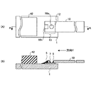
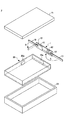
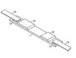
図7は電池パックの分解斜視図を示す。
【0004】
電池パック2は主に、電池本体20、保護回路基板1、ケース蓋21、ケース23から構成されている。
【0005】
電池本体20は、例えば、リチウムイオン蓄電池から構成されている。保護回路基板1は、電池本体20とここでは図示しない外部端子との間に接続されており、充電時及び放電時の電池本体20の電圧を監視して、電池本体20の充放電を制御し、電池本体20の保護を行うための回路が搭載され、電池本体20とは端子板10により接続されている。端子板10の一端は、電池本体20にスポット溶接され、他端は保護回路基板1に半田付けされている。
【0006】
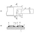
保護回路基板1は、例えば、多層プリント配線基板から構成されており、封止されたIC(integrated circuit)チップなどの電子部品42を搭載し、端子板10が半田付けされている。保護回路基板1はこの状態で、電池パック2の組み立て先に提供される。
【0007】
組み立て先では、提供された保護回路基板1と電池本体20との接続を行うための端子板10の一端をスポット溶接する。端子板10の一端は、矢印A、B方向に示すように折曲されつつ、多端が電池本体20にスポット溶接される。
【0008】
従来の保護回路基板における端子板、例えばニッケル板の取付け機構の一例を図8、9に示す。同図中、図7と同一構成部分には同一符号を付しその説明は省略する。
【0009】
図9は、接着前の保護回路基板1及び端子10を示す。保護回路基板1の長手方向端側の略中央に、銅箔(以下ランドという)12、該ランド12の表面にあらかじめ塗布された半田クリーム15、こちらもあらかじめ端子10の表面に施された半田めっき14、端子10の順で積層されている。
【0010】
端子板10と前記ランド12に挟まれた半田めっき及び半田クリームはリフローによって溶融され前記端子10の端面になじみ、広がりに断面形略三角形状を呈して付着する。この三角形状の半田が冷却されて後述するフィレットとなる。
【0011】
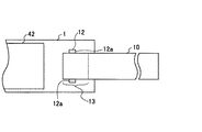
図10(A)は硬化後の保護回路基板1及び端子板10の平面図を、図10(B)は同図(A)のC−C線断面図を、図11は図10(A)のD−D線断面図を示す。他端については同一の取り付け機構であるため図を省略した。
【0012】
端子板10の一端10gは保護回路基板1の長手方向と垂直な端面の略中央と半田により固定されており、端子板10の他端は電池本体20と接続されるため自由端となっている。前記半田は、リフローによる加熱後、保護回路基板側端面になじみ、冷却工程により硬化して、端面10gにフィレット5を形成する。剥離強度を向上させるためには、該フィレット5を形成することが有効であるとされている。
【0013】
図12は図10の変形例であり、凹状の端面形状としたものを示す。図12(B)は、同図(A)のE‐E線断面図を示す。保護回路基板側端面に凹状の端面10hを有する端子10が、保護回路基板の長手方向と垂直な端面の略中央と半田により固定されており、端子板10の他端は電池本体20と接続されるため自由端となっている。
【0014】
端子板10の端面10hを凹状に形成したことに伴い、リフローにより加熱された半田が、保護回路基板側端面10hになじみ、冷却工程により硬化して、凹状部分にフィレット5が形成される。端面を凹状とすることでフィレット5が形成される部分が増大し、端面10gよりも剥離強度が増している。また、図13に示すように、ランド12に突起部12aを形成して、フィレットが形成される部分を増すことが考えられた(例えば、特許文献1参照)。
【0015】
【特許文献】
特開平2002−26498(図1)
【0016】
【発明が解決しようとする課題】
前記図7における上記従来の保護回路基板1における端子10の取り付け機構は、保護回路基板1と電池本体20との接続を行うために端子板10の一端を、矢印A、B方向に示すように折曲される際、端子板10が半田付け部13から剥離することがあった。
【0017】
前述のとおり、剥離強度を向上させるためには、端子10の保護回路基板側端面にフィレット5を形成することが有効であるとされていたため、図12に示す例えば凹状の端面形状の端子10hや、図13に示すようにランドに突起部12aを用い、形成されるフィレット部を増大することが考えられた。しかしながら、フィレット5を形成する部分の増大により剥離強度が増すものの、なお、端子板10の折曲等により、半田付け部が剥離するという問題があった。これは、図10において、フィレット5の形成面が端子10の保護回路基板側端面に向かっている(方向X)ため、図10(B)において、端子10の自由端を上方へ動かした場合(C)、ランド12及び端子10が剥離するためである。
【0018】
なお、端子10の保護回路基板側の端側を上方に動かして端子10を剥離させる力(D)は、フィレット5が存在するため働かない。
【0019】
また、前記半田めっき及び半田クリームがリフローによって溶融され前記端子10の端面になじみ広がる過程において、凹状の端面10hを取り囲む液状化した半田による不均一な圧力や、半田の冷却、硬化時に前記端子の位置がずれる可能性があり、より位置ずれしにくい端子の取り付け機構が求められていた。
【0020】
本発明は上記の点に鑑みてなされたもので、取付け強度の高い端子構造及び回路保護基板、位置ずれしにくい端子の取り付け機構を提供することができる。
【0021】
【課題を解決するための手段】
本発明は、基板(1)と半田付けされる端子(10)の端子構造において、前記回路保護基板(1)と半田付けされる半田付け部(13)に、穴部(10a)又は切り欠き部(10b)を有することを特徴とする。
【0022】
本発明によれば、該穴部(10a)又は切り欠き部(10d)の内側にフィレット(5)が形成され、端子(10)の自由端に向く側にフィレット(7)が形成される。この方向にフィレットが形成されると、基板側端面(10g)に形成されるフィレット(5)よりも、端子の屈曲、変形などに関し剥離強度が向上する。
【0023】
また、前記半田めっき(14)及び半田クリーム(15)がリフローによって溶融されなじみ広がる過程において、溶融した半田が穴部(10a)又は切り欠き部(10d)に流れ込むため、半田付け部(13)を囲む溶融した半田からうける不均一な圧力が吸収され、端子(10)の位置ずれが縮小する。
【0024】
前記凹状端面10hと同時に、穴部(10a)又は切り欠き部(10b)を有することでフィレット(5)が増大するため、端子の屈曲、変形などに関し剥離強度が向上する。
【0025】
また、端子(10)の半田付け部(13)に切り欠き部(10d)を設けると、切り欠き部に応力が集中しやすくなるため端子の屈曲等に対し切り欠き部(10d)で屈曲しやすくなり、結果剥離しにくくなる。
【0026】
なお、上記参照符号はあくまでも参考であり、これによって、特許請求の範囲が限定されるものではない。
【0027】
【発明の実施の形態】
〔第1実施例〕
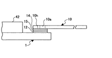
図1(A)は、本発明の第1実施例の形態として半田付け部(13)に円形の穴部(くりぬき部)を設けた基板及び端子の平面図を示す。なお、図12と同一構成部分には同一符号を付し、その説明は省略する。
本実施例の端子10は、保護回路基板側の半田付け部の略中央に円形の穴部10aを備える。
【0028】
図2は、接着前のプリント基板1及び端子10の側面図を、図1(B)は接着後の図1(A)のA−A線断面図を示す。なお、図1(B)においては硬化後に端子10とランド12間に介在し残留する半田は省略した。また、同図中、図9及び図10と同一構成部分には同一符号を付し、その説明は省略する。
【0029】
本実施例では、リフロー炉による加熱によって溶融した半田めっき14及び半田クリーム15が端子10の端面10h及び円形の穴部10aの内側になじみ、広がり断面形略三角形状を呈して付着する。更に、該半田は、前記加熱後の冷却工程により硬化してフィレット5及び7を形成する。
【0030】
本実施例では、前記端子10の自由端に向く端面にフィレット7が形成される点に特徴がある。これにより、端子10の自由端を上方へ動かすときに発生する剥離に対して強度を増すことができる。
【0031】
なお、フィレット7は正確に端子10の自由端に向く端面に形成されていなくても剥離強度の向上が期待できる。
【0032】
また、本実施例によれば、前記半田めっき14及び半田クリーム15がリフローによって溶融されなじみ広がる過程において、溶融した半田が穴部10aに流れ込むため、半田付け部13を囲む溶融した半田からうける不均一な圧力が吸収され、端子10の位置ずれが縮小する。
【0033】
本実施例に関しては、種々の変形例が考案できる。
【0034】
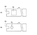
図3(A)は、保護回路基板側に長方形の穴部10bを備えた端子10である。
【0035】
本変形例では、前記端子10の自由端に向く側にフィレット7が形成される。自由端に向くフィレット7は、端子10を上方へ動かすことにより発生する剥離に対し強度を増加させる。
【0036】
図3(B)は、保護回路基板側に楕円形状の穴部10cを備えた端子10の平面図を示す。
【0037】
本変形例では、前記端子10の自由端に向く側にフィレット7が形成される。自由端に向く側のフィレットは剥離強度を向上させることができる。また、長方形状とした穴部10bでは、端子の屈曲、変形などに関し、長方形が有する4つの角部に応力が集中する恐れがあるが、本変形例の楕円形状の穴部10cでは応力の集中が軽減できる。
【0038】
なお、本変形例は、穴部の形状として長方形状、楕円形状に限られるものではなく、多角形状、星型形状などでも良い。
【0039】
〔第2実施例〕
図4(A)は、本発明の第2実施例の平面図、同(B)は本発明の第2実施例の図4(A)におけるB−B線断面図を示す。なお、図4(B)においては硬化後に端子10とランド12間に介在し残留する半田は省略した。同図中、図1と同一構成部分には同一符号を付し、その説明は省略する。
【0040】
本実施例では、端子10が保護回路基板側の半田付け部13に切り欠き部10dを備える点で第1実施例と異なる。
【0041】
リフロー炉による加熱によって溶融した半田めっき14及び半田クリーム15が端子10の切り欠き部10dの内側になじみ、広がり断面形略三角形状を呈して付着する。更に、該半田は、前記加熱後の冷却工程により硬化してフィレット7を形成する。
【0042】
第1実施例で前述したとおり、端子10の自由端に向く方向にフィレット7が形成されると、保護回路基板側端面10gに形成されるフィレット5よりも、端子の屈曲、変形などに関し、剥離強度が確保される。なお、フィレット7が正確に端子10の自由端に向く方向でなくても剥離強度の向上が期待できる。
【0043】
また、本実施例によれば、前記半田めっき14及び半田クリーム15がリフローによって溶融されなじみ広がる過程において、溶融した半田が切り欠き部10dに流れ込むため、半田付け部13を囲む溶融した半田からうける不均一な圧力が吸収され、端子10の位置ずれが縮小する。
【0044】
また、該実施例では切り欠き部に応力が集中しやすくなるため端子の屈曲等に対し切り欠き部で屈曲しやすくなり、その結果、剥離しにくくなるという特徴がある。
【0045】
本実施例に関しては、種々の変形例が考案できる。
【0046】
図5(A)は、保護回路基板側の半田付け部13に矩形の切り欠き部10eを備えた端子10の平面図である。
【0047】
本変形例では、前記端子10の自由端に向く側にフィレット7が形成されるが、自由端に向くフィレット7は、剥離強度を向上させることができる。
【0048】
図5(B)は、保護回路基板側の半田付け部13にU字形乃至半楕円形状の切り欠き部10fを備えた端子10の平面図である。
【0049】
本変形例では、前記端子10の自由端に向く側にフィレット7が形成されるが、自由端に向く側のフィレットは、剥離強度を向上させることができる。また、矩形状とした切り欠き部10eでは、端子の屈曲、変形などに関し、矩形が有する角部に応力が集中する恐れがあるが、本変形例では応力の集中が軽減できるため、端子10の破断の恐れが軽減できる。
【0050】
図5(C)は、保護回路基板側の半田付け部13に切り欠き部を二対備えた端子10の平面図である。
【0051】
本変形例では、前記端子10の自由端に向く側にフィレット7が形成されるとともに、形成されるフィレット部分が増大し剥離強度が増す。同時に屈曲性が向上するという特徴がある。また二対の切り欠き部のうち、基板側端面に近い切り欠き部にフィレット7を形成しもう一方の切り欠き部を簡略化した形状、例えば切り込みにするなどの変形例も考えられる。該実施例では製造行程を簡易化する効果がある。
【0052】
なお、本変形例は、切り欠き部の形状としてV字乃至三角形状、U字乃至半楕円形状に限られるものではなく、多角形状などでも良い。
【0053】
〔第3実施例〕
図6は、本発明の第3実施例の平面図を示す。なお、同図中、図5と同一構成部分には同一符号を付し、その説明は省略する。
【0054】
本実施例では、保護回路基板側の半田付け部13に穴部10aとともに切り欠き部10bを備える点で第1、2実施例と異なる。
【0055】
前述の通り、端子10の自由端に向く側にフィレット7が形成されることで、保護回路基板側端面10gに形成されるフィレット5よりも、端子の屈曲、変形などに関し、剥離強度が確保される。また、穴部のみ又は切り欠き部のみの形状よりも形成されるフィレット5及び7を増大できるので、第1、2実施例よりも剥離強度を向上させることができる。
【0056】
また、本実施例によれば、前記半田めっき14及び半田クリーム15がリフローによって溶融されなじみ広がる過程において、溶融した半田が穴部及び切り欠き部に流れ込むため、半田付け部13を囲む溶融した半田からうける不均一な圧力が吸収され、端子10の位置ずれが縮小する。
【0057】
また、本実施例では切り欠き部に応力が集中しやすくなるため端子の屈曲等に対し切り欠き部で屈曲しやすくなり、結果剥離しにくくなるという特徴がある。
【0058】
なお、本実施例においても、穴部の形状として、長方形状、楕円形状、多角形状、星型形状などでも良く、切り欠き部の形状として、V字乃至三角形状、U字乃至半楕円形状、多角形状などでも良い。
【0059】
而して、本発明は、本発明の精神を逸脱しない限り種々の改変を為すことができ、そして本発明が該改変されたものに及ぶことは当然である。
【発明の効果】
以上詳細に説明したように、本発明は、取り付け強度の高い端子構造及び二次電池保護回路を提供する。
【図面の簡単な説明】
【図1】本発明の第1実施例の平面図及び断面図である。
【図2】本発明の第1実施例の側面図である。
【図3】本発明の第1実施例の変形例である端子10の平面図である。
【図4】本発明の第2実施例の平面図及び断面図である。
【図5】本発明の第2実施例の変形例である端子10の平面図である。
【図6】本発明の第3実施例である端子10の平面図である。
【図7】電池パックの分解斜視図である。
【図8】保護回路基板の斜視図である。
【図9】従来発明の側面図である。
【図10】従来技術の平面図及び断面図である。
【図11】図10(A)のD−D線断面図である。
【図12】従来技術の平面図及び断面図である。
【図13】従来技術の平面図である。
【符号の説明】
1 プリント基板
2 電池パック
5 半田付けされる端面に形成されたフィレット
7 自由端に向く端面に形成されたフィレット
端子
10a 円形状の穴部
10b 四角形状の穴部
10c 楕円形状の穴部
10d 三角形状の切り欠き部
10e 矩形状の切り欠き部
10f 半楕円形状の切り欠き部
10g 端面
10h 凹状の端面
12 ランド
12a ランドの突起部
13 半田付け部
半田めっき
クリーム半田
20 2次電池本体
20a 2次電池の電極
21 電池ケースの蓋
23 電池ケース
42 封止されたICチップ[0001]
TECHNICAL FIELD OF THE INVENTION
The present invention relates to a terminal structure of a circuit board and a secondary battery protection circuit, and more particularly to an improvement in mounting strength of a terminal to be soldered to the board.
[0002]
[Prior art]
2. Description of the Related Art In recent years, mobile terminal devices such as mobile phones are equipped with a battery pack as a driving source.
[0003]
FIG. 7 is an exploded perspective view of the battery pack.
[0004]
The
[0005]
The battery
[0006]
The
[0007]
At the assembly destination, one end of the
[0008]
FIGS. 8 and 9 show an example of a mounting mechanism of a terminal plate, for example, a nickel plate in a conventional protection circuit board. 7, the same components as those of FIG. 7 are denoted by the same reference numerals, and the description thereof will be omitted.
[0009]
FIG. 9 shows the
[0010]
The solder plating and the solder cream sandwiched between the
[0011]
10A is a plan view of the
[0012]
One
[0013]
FIG. 12 shows a modified example of FIG. 10 in which a concave end surface is formed. FIG. 12B is a sectional view taken along line EE of FIG. A
[0014]
With the
[0015]
[Patent Document]
JP-A-2002-26498 (FIG. 1)
[0016]
[Problems to be solved by the invention]
In the conventional
[0017]
As described above, it has been considered effective to form the
[0018]
The force (D) for moving the end of the terminal 10 on the side of the protection circuit board upward to detach the terminal 10 does not work because the
[0019]
Further, in the process in which the solder plating and the solder cream are melted by reflow and spread over the end face of the terminal 10, uneven pressure due to liquefied solder surrounding the
[0020]
The present invention has been made in view of the above points, and can provide a terminal structure with high mounting strength, a circuit protection board, and a terminal mounting mechanism that is less likely to be displaced.
[0021]
[Means for Solving the Problems]
According to the present invention, in a terminal structure of a terminal (10) to be soldered to a substrate (1), a hole (10a) or a notch is formed in a soldering portion (13) to be soldered to the circuit protection substrate (1). (10b).
[0022]
According to the present invention, the fillet (5) is formed inside the hole (10a) or the notch (10d), and the fillet (7) is formed on the side facing the free end of the terminal (10). When the fillet is formed in this direction, the peel strength with respect to the bending and deformation of the terminal is improved as compared with the fillet (5) formed on the substrate side end surface (10g).
[0023]
Further, in a process in which the solder plating (14) and the solder cream (15) are melted and spread by reflow, the melted solder flows into the hole (10a) or the cutout (10d). The uneven pressure received from the molten solder surrounding the terminal is absorbed, and the displacement of the terminal (10) is reduced.
[0024]
Since the fillet (5) is increased by having the hole (10a) or the cutout (10b) at the same time as the
[0025]
Further, when the notch portion (10d) is provided in the soldering portion (13) of the terminal (10), stress tends to concentrate on the notch portion, so that the terminal bends at the notch portion (10d) against bending or the like. It is easy to peel off as a result.
[0026]
Note that the above reference numerals are for reference only, and do not limit the scope of the claims.
[0027]
BEST MODE FOR CARRYING OUT THE INVENTION
[First embodiment]
FIG. 1A is a plan view of a substrate and a terminal in which a circular hole (opening) is provided in a soldering portion (13) as an embodiment of the first embodiment of the present invention. The same components as those in FIG. 12 are denoted by the same reference numerals, and description thereof will be omitted.
The terminal 10 of this embodiment has a
[0028]
FIG. 2 is a side view of the printed
[0029]
In the present embodiment, the solder plating 14 and the
[0030]
The present embodiment is characterized in that a
[0031]
Note that even if the
[0032]
Further, according to the present embodiment, in a process in which the solder plating 14 and the
[0033]
Regarding the present embodiment, various modifications can be devised.
[0034]
FIG. 3A shows a terminal 10 having a
[0035]
In this modification, a
[0036]
FIG. 3B is a plan view of the terminal 10 having the
[0037]
In this modification, a
[0038]
In this modification, the shape of the hole is not limited to a rectangle or an ellipse, but may be a polygon, a star, or the like.
[0039]
[Second embodiment]
FIG. 4A is a plan view of a second embodiment of the present invention, and FIG. 4B is a cross-sectional view taken along the line BB of FIG. 4A of the second embodiment of the present invention. In FIG. 4B, the solder remaining between the terminal 10 and the
[0040]
This embodiment is different from the first embodiment in that the terminal 10 has a
[0041]
The solder plating 14 and the
[0042]
As described above in the first embodiment, when the
[0043]
Further, according to the present embodiment, in a process in which the solder plating 14 and the
[0044]
Further, in this embodiment, the stress is easily concentrated on the notch, so that the terminal is easily bent at the notch with respect to the bending of the terminal and the like, and as a result, it is difficult to peel off.
[0045]
Regarding the present embodiment, various modifications can be devised.
[0046]
FIG. 5A is a plan view of the terminal 10 having the
[0047]
In the present modification, the
[0048]
FIG. 5B is a plan view of the terminal 10 having the U-shaped or
[0049]
In this modification, the
[0050]
FIG. 5C is a plan view of the terminal 10 having two notches in the
[0051]
In the present modified example, the
[0052]
In this modification, the shape of the cutout portion is not limited to the V-shaped or triangular shape, the U-shaped or semi-elliptical shape, and may be a polygonal shape.
[0053]
[Third embodiment]
FIG. 6 shows a plan view of a third embodiment of the present invention. 5, the same components as those of FIG. 5 are denoted by the same reference numerals, and the description thereof will be omitted.
[0054]
This embodiment is different from the first and second embodiments in that a
[0055]
As described above, since the
[0056]
Further, according to the present embodiment, in the process where the solder plating 14 and the
[0057]
Further, in the present embodiment, the stress is easily concentrated on the notch, so that the terminal is easily bent at the notch with respect to the bending of the terminal and the like, and as a result, it is difficult to peel off.
[0058]
In the present embodiment, the hole may have a rectangular shape, an elliptical shape, a polygonal shape, a star shape, or the like. A polygonal shape may be used.
[0059]
Thus, the present invention can be variously modified without departing from the spirit of the present invention, and it goes without saying that the present invention extends to the modifications.
【The invention's effect】
As described in detail above, the present invention provides a terminal structure and a secondary battery protection circuit with high mounting strength.
[Brief description of the drawings]
FIG. 1 is a plan view and a sectional view of a first embodiment of the present invention.
FIG. 2 is a side view of the first embodiment of the present invention.
FIG. 3 is a plan view of a terminal 10 which is a modification of the first embodiment of the present invention.
FIG. 4 is a plan view and a sectional view of a second embodiment of the present invention.
FIG. 5 is a plan view of a terminal 10 which is a modification of the second embodiment of the present invention.
FIG. 6 is a plan view of a terminal 10 according to a third embodiment of the present invention.
FIG. 7 is an exploded perspective view of the battery pack.
FIG. 8 is a perspective view of a protection circuit board.
FIG. 9 is a side view of a conventional invention.
FIG. 10 is a plan view and a sectional view of a conventional technique.
FIG. 11 is a sectional view taken along line DD of FIG.
FIG. 12 is a plan view and a cross-sectional view of a conventional technique.
FIG. 13 is a plan view of the prior art.
[Explanation of symbols]
DESCRIPTION OF
Claims (3)
前記基板と半田付けされる半田付け部に、穴部又は切り欠き部を有することを特徴とする端子構造。In the terminal structure of the terminal soldered to the board,
A terminal structure having a hole or a notch in a soldering portion to be soldered to the substrate.
Priority Applications (1)
| Application Number | Priority Date | Filing Date | Title |
|---|---|---|---|
| JP2003096345A JP2004303618A (en) | 2003-03-31 | 2003-03-31 | Terminal structure and secondary battery protection circuit |
Applications Claiming Priority (1)
| Application Number | Priority Date | Filing Date | Title |
|---|---|---|---|
| JP2003096345A JP2004303618A (en) | 2003-03-31 | 2003-03-31 | Terminal structure and secondary battery protection circuit |
Publications (1)
| Publication Number | Publication Date |
|---|---|
| JP2004303618A true JP2004303618A (en) | 2004-10-28 |
Family
ID=33408444
Family Applications (1)
| Application Number | Title | Priority Date | Filing Date |
|---|---|---|---|
| JP2003096345A Pending JP2004303618A (en) | 2003-03-31 | 2003-03-31 | Terminal structure and secondary battery protection circuit |
Country Status (1)
| Country | Link |
|---|---|
| JP (1) | JP2004303618A (en) |
Cited By (13)
| Publication number | Priority date | Publication date | Assignee | Title |
|---|---|---|---|---|
| JP2007026813A (en) * | 2005-07-14 | 2007-02-01 | Nichicon Corp | Terminal board, and protective circuit unit of secondary battery equipped with it |
| JP2009146600A (en) * | 2007-12-11 | 2009-07-02 | Nec Tokin Corp | Protection circuit module |
| KR100965683B1 (en) | 2008-03-31 | 2010-06-24 | 삼성에스디아이 주식회사 | Battery pack |
| KR101023879B1 (en) * | 2008-12-18 | 2011-03-22 | 삼성에스디아이 주식회사 | Secondary battery with protection circuit module |
| CN102315407A (en) * | 2010-07-01 | 2012-01-11 | 通用汽车环球科技运作有限责任公司 | The battery fin connects and manufacturing approach |
| US8369095B2 (en) | 2007-09-28 | 2013-02-05 | Samsung Sdi Co., Ltd. | Protection circuit board for secondary battery and secondary battery using the protection circuit board |
| KR101315949B1 (en) * | 2012-04-09 | 2013-10-08 | 지에스피 주식회사 | Soldering method for nickel-terminal of battery protection circuit board and soldering jig thereof |
| US8632900B2 (en) | 2008-09-22 | 2014-01-21 | Samsung Sdi Co., Ltd. | Secondary battery |
| CN103531741A (en) * | 2013-09-24 | 2014-01-22 | 北京鼎能开源电池科技股份有限公司 | Lithium ion battery negative electrode tab component, manufacturing method thereof and lithium ion battery |
| US8703327B2 (en) | 2008-06-20 | 2014-04-22 | Samsung Sdi Co., Ltd. | Rechargeable battery and manufacturing method thereof |
| US9065083B2 (en) | 2008-06-03 | 2015-06-23 | Samsung Sdi Co., Ltd. | Lithium polymer battery |
| JP6297199B1 (en) * | 2017-01-12 | 2018-03-20 | 日本碍子株式会社 | End current collecting member and cell stack device |
| KR20210070127A (en) * | 2019-12-04 | 2021-06-14 | 주식회사 파워로직스 | Protect circuit module and method of manufacturing the same |
-
2003
- 2003-03-31 JP JP2003096345A patent/JP2004303618A/en active Pending
Cited By (16)
| Publication number | Priority date | Publication date | Assignee | Title |
|---|---|---|---|---|
| JP2007026813A (en) * | 2005-07-14 | 2007-02-01 | Nichicon Corp | Terminal board, and protective circuit unit of secondary battery equipped with it |
| US8369095B2 (en) | 2007-09-28 | 2013-02-05 | Samsung Sdi Co., Ltd. | Protection circuit board for secondary battery and secondary battery using the protection circuit board |
| JP2009146600A (en) * | 2007-12-11 | 2009-07-02 | Nec Tokin Corp | Protection circuit module |
| KR100965683B1 (en) | 2008-03-31 | 2010-06-24 | 삼성에스디아이 주식회사 | Battery pack |
| US8795865B2 (en) | 2008-03-31 | 2014-08-05 | Samsung Sdi Co., Ltd. | Battery pack |
| US9065083B2 (en) | 2008-06-03 | 2015-06-23 | Samsung Sdi Co., Ltd. | Lithium polymer battery |
| US8703327B2 (en) | 2008-06-20 | 2014-04-22 | Samsung Sdi Co., Ltd. | Rechargeable battery and manufacturing method thereof |
| US8632900B2 (en) | 2008-09-22 | 2014-01-21 | Samsung Sdi Co., Ltd. | Secondary battery |
| KR101023879B1 (en) * | 2008-12-18 | 2011-03-22 | 삼성에스디아이 주식회사 | Secondary battery with protection circuit module |
| US8685552B2 (en) | 2008-12-18 | 2014-04-01 | Samsung Sdi Co., Ltd. | Secondary battery including protection circuit module |
| CN102315407A (en) * | 2010-07-01 | 2012-01-11 | 通用汽车环球科技运作有限责任公司 | The battery fin connects and manufacturing approach |
| KR101315949B1 (en) * | 2012-04-09 | 2013-10-08 | 지에스피 주식회사 | Soldering method for nickel-terminal of battery protection circuit board and soldering jig thereof |
| CN103531741A (en) * | 2013-09-24 | 2014-01-22 | 北京鼎能开源电池科技股份有限公司 | Lithium ion battery negative electrode tab component, manufacturing method thereof and lithium ion battery |
| JP6297199B1 (en) * | 2017-01-12 | 2018-03-20 | 日本碍子株式会社 | End current collecting member and cell stack device |
| KR20210070127A (en) * | 2019-12-04 | 2021-06-14 | 주식회사 파워로직스 | Protect circuit module and method of manufacturing the same |
| KR102378294B1 (en) * | 2019-12-04 | 2022-03-25 | 주식회사 파워로직스 | Protect circuit module and method of manufacturing the same |
Similar Documents
| Publication | Publication Date | Title |
|---|---|---|
| US8199527B2 (en) | Electronic component and manufacturing method therefor | |
| JP2004303618A (en) | Terminal structure and secondary battery protection circuit | |
| JP2001148594A (en) | Electronic device with shield case | |
| JP4098556B2 (en) | Terminal board, circuit board provided with the terminal board, and method for connecting the terminal board | |
| JP2000124588A (en) | Electronic circuit unit and manufacture of it | |
| US8727810B2 (en) | Connector | |
| JP2010252538A (en) | Battery protection module and lead thermistor mounting method | |
| JP2001110925A (en) | Conductive cap, electronic component, and method of forming insulating film on conductive cap | |
| JP5869282B2 (en) | Electrical connector | |
| KR20060069509A (en) | Circuit board | |
| US20110155450A1 (en) | Printed circuit board and electronic apparatus | |
| JP2003078278A (en) | Electronic component with shield case | |
| KR19980024072A (en) | Semiconductor device and mounting method thereof | |
| JP2001148595A (en) | Electronic device with shield case | |
| EP3419393A1 (en) | Electronic device and manufacturing method therefor | |
| US9414492B2 (en) | Printed wiring board and electric tool switch provided therewith | |
| JP4016197B2 (en) | Circuit board, method of connecting terminals to circuit board, and method of manufacturing battery pack | |
| TWM643074U (en) | Circuit board structure | |
| JP3807874B2 (en) | Electronic circuit unit | |
| JP4844260B2 (en) | Electronic component and manufacturing method thereof | |
| JP2008198887A (en) | Shield case mounting structure and shield case fitting method | |
| JP2687899B2 (en) | Surface mount type terminal | |
| WO2020003908A1 (en) | Wiring board and electronic component mounted substrate | |
| JP4877455B2 (en) | Secondary battery protection module and lead mounting method | |
| JP2004014721A (en) | Surface mounting electronic component and printed circuit board |
Legal Events
| Date | Code | Title | Description |
|---|---|---|---|
| A621 | Written request for application examination |
Free format text: JAPANESE INTERMEDIATE CODE: A621 Effective date: 20050624 |
|
| A977 | Report on retrieval |
Free format text: JAPANESE INTERMEDIATE CODE: A971007 Effective date: 20070620 |
|
| A131 | Notification of reasons for refusal |
Free format text: JAPANESE INTERMEDIATE CODE: A131 Effective date: 20090113 |
|
| A521 | Request for written amendment filed |
Free format text: JAPANESE INTERMEDIATE CODE: A523 Effective date: 20090219 |
|
| A131 | Notification of reasons for refusal |
Free format text: JAPANESE INTERMEDIATE CODE: A131 Effective date: 20090407 |
|
| A02 | Decision of refusal |
Free format text: JAPANESE INTERMEDIATE CODE: A02 Effective date: 20090804 |