JP2004294841A - Antireflection film - Google Patents
Antireflection film Download PDFInfo
- Publication number
- JP2004294841A JP2004294841A JP2003087864A JP2003087864A JP2004294841A JP 2004294841 A JP2004294841 A JP 2004294841A JP 2003087864 A JP2003087864 A JP 2003087864A JP 2003087864 A JP2003087864 A JP 2003087864A JP 2004294841 A JP2004294841 A JP 2004294841A
- Authority
- JP
- Japan
- Prior art keywords
- layer
- film
- antireflection
- refractive index
- films
- Prior art date
- Legal status (The legal status is an assumption and is not a legal conclusion. Google has not performed a legal analysis and makes no representation as to the accuracy of the status listed.)
- Granted
Links
Images


Landscapes
- Surface Treatment Of Optical Elements (AREA)
- Laminated Bodies (AREA)
Abstract
Description
【0001】
【発明の属する技術分野】
この発明は、入射光の反射を防止する反射防止膜に関し、特に、近赤外領域において、広波長帯域の光の反射を防止する反射防止膜に関する。
【0002】
【従来の技術】
光が屈折率の異なる2つの媒質を伝播する場合、この境界面に入射した光の一部(例えば、空気とガラスとの境界の場合、入射光の約4%)は反射する。そして、光学部品において、反射ロスや戻り光の影響がある場合、最適な特性が得られないことがある。
そのため、現在広く使用されている光学部品では、光の入射又は出射が行われる媒質境界面に反射防止膜(ARコート)が成膜されることが一般的である。ここで「反射防止膜」とは、物質の表面での光の反射を防止する光学的に透明な膜をいい、従来、屈折率の異なる複数の膜を2層から4層程度積層したものが一般的であった。
【0003】
しかし、従来の反射防止膜では、使用される波長帯域の中心波長に対して±50nm程度の帯域幅でしか十分な反射防止特性を得ることができないという問題点がある。
特に、近年、1.3μm帯や1.5μm帯を利用した光通信網の普及が進んでおり、これらの用途では100nm程度の波長帯域幅が使用されることが一般的である。そのため、従来の反射防止膜では、反射防止帯域に余裕がなく、製造誤差や使用環境等によっては、最適な特性を得ることができない場合もある。また、複数の波長帯域で共用して利用する光学部品の場合、それに使用される反射防止膜には、利用されるすべての波長帯域での反射防止特性が要求される。しかし、中心波長に対して±50nm程度の帯域幅でしか十分な反射防止特性を得ることができない従来の反射防止膜では、到底、このような用途に用いることはできない。
【0004】
これに対し、特許文献1では、複数種の屈折率の異なる材料からなる薄膜を積層形成した多層構造の反射防止膜であって、所要波長帯域において反射率の低い2つの谷と、その間に反射率ピークを有する広帯域な低反射率特性を有する多層反射防止膜が提唱され、これにより広帯域の反射防止特性が実現されている。
【0005】
【特許文献1】
特開平10−186104号公報
【0006】
【発明が解決しようとする課題】
しかし、特許文献1の反射防止膜では、広帯域かつ平坦な(リップルが小さい)反射防止特性を得ることが不可能であるという問題点がある。
すなわち、特許文献1の反射防止膜は、反射率の低い2つの谷と、その間に反射率ピークを有する反射率特性を有し、この反射率ピーク点を目標反射率以下に抑えることにより、その両側に位置する反射率の低い2つの谷を含む波長帯域での反射率を目標反射率以下に抑えている。従って、この反射防止膜の反射防止特性には、必ず、反射率ピーク点と反射率の低い2つの谷との間に反射特性差が生じることになる。
この発明は、以上のような点に鑑みてなされたものであり、広い帯域での反射防止特性を得ることができ、この広い帯域において反射防止特性のリップルを低減し得る反射防止膜を提供することを目的とする。
【0007】
【課題を解決するための手段】
この発明では上記課題を解決するために、反射防止帯域の設計中心波長λに対する屈折率n1が1.4≦n1≦1.5の関係を満たす低屈折率膜と、この中心波長λに対する屈折率n2が1.9≦n2≦2.4の関係を満たす高屈折率膜とを、基板側から入射光側へ、交互に合計9層積層してなる反射防止膜が提供される。ここで、この反射防止膜の基板側から入射光側へ数えた第1層、第3相、第5層、第7層及び第9層は低屈折率膜であり、第2層、第4層、第6層及び第8層は高屈折率膜である。また、第1層から第9層までの各光学的膜厚nd1、nd2、nd3、nd4、nd5、nd6、nd7、nd8、nd9は、0.355λ≦nd1≦0.385λ、0.014λ≦nd2≦0.016λ、0.069λ≦nd3≦0.081λ、0.218λ≦nd4≦0.232λ、0.181λ≦nd5≦0.188λ、0.020λ≦nd6≦0.026λ、0.077λ≦nd7≦0.080λ、0.117λ≦nd8≦0.124λ、0.158λ≦nd9≦0.167λの関係を満たす。
【0008】
これにより、設計中心周波数λ=1.5μm、波長帯域幅300nmにおいて、反射率0.7%以下の反射防止特性を得ることができ、また、最適化を行うことにより、同条件下、反射率0.1%以下、リップル±0.01%以下の反射防止特性を得ることができる。
また、好ましくは、この発明の反射防止膜は、SiO2膜とTa2O5膜とを、基板側から入射光側へ、交互に合計9層積層してなり、基板側から入射光側へ数えた第1層、第3相、第5層、第7層及び第9層はSiO2膜であり、第2層、第4層、第6層及び第8層はTa2O5膜であり、反射防止帯域の設計中心波長をλとし、第1層から第9層までの各光学的膜厚を順にnd1、nd2、nd3、nd4、nd5、nd6、nd7、nd8、nd9とした場合に、0.355λ≦nd1≦0.385λ、0.014λ≦nd2≦0.017λ、0.067λ≦nd3≦0.081λ、0.215λ≦nd4≦0.232λ、0.181λ≦nd5≦0.196λ、0.019λ≦nd6≦0.026λ、0.077λ≦nd7≦0.083λ、0.117λ≦nd8≦0.127λ、0.154λ≦nd9≦0.167λの関係を満たす。
【0009】
さらに、好ましくは、この発明の反射防止膜は、SiO2膜とTiO2膜とを、基板側から入射光側へ、交互に合計9層積層してなり、基板側から入射光側へ数えた第1層、第3相、第5層、第7層及び第9層はSiO2膜であり、第2層、第4層、第6層及び第8層はTiO2膜であり、反射防止帯域の設計中心波長をλとし、第1層から第9層までの各光学的膜厚を順にnd1、nd2、nd3、nd4、nd5、nd6、nd7、nd8、nd9とした場合に、0.355λ≦nd1≦0.401λ、0.014λ≦nd2≦0.016λ、0.069λ≦nd3≦0.081λ、0.218λ≦nd4≦0.236λ、0.174λ≦nd5≦0.188λ、0.020λ≦nd6≦0.026λ、0.074λ≦nd7≦0.080λ、0.114λ≦nd8≦0.124λ、0.158λ≦nd9≦0.171λの関係を満たす。
また、この発明において、好ましくは、設計中心波長λは、1μm≦λ≦1.7μmの関係を満たす。
【0010】
【発明の実施の形態】
以下、この発明の実施の形態を図面を参照して説明する。なお、この発明は以下の実施の形態及び実施例に限定されるものではない。
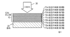
図1は、この形態における反射防止膜10の構成を例示した断面図である。
図1に例示するように、この例の反射防止膜10は、光学部品の基板20の表面に成膜された低屈折率膜11a(第1層)、低屈折率膜11aの光学部品20と反対の面に成膜された高屈折率膜12a(第2層)、高屈折率膜12aの低屈折率膜11aと反対の面に成膜された低屈折率膜11b(第3層)、低屈折率膜11bの高屈折率膜12aと反対の面に成膜された高屈折率膜12b(第4層)、高屈折率膜12bの低屈折率膜11bと反対の面に成膜された低屈折率膜11c(第5層)、低屈折率膜11cの高屈折率膜12bと反対の面に成膜された高屈折率膜12c(第6層)、高屈折率膜12cの低屈折率膜11cと反対の面に成膜された低屈折率膜11d(第7層)、低屈折率膜11dの高屈折率膜12cと反対の面に成膜された高屈折率膜12d(第8層)、及び高屈折率膜12dの低屈折率膜11dと反対の面に成膜された低屈折率膜11e(第9層)によって構成され、基板20表面へ入射する入射光30の反射を防止する。ここで、この例の場合、反射防止帯域の設計中心波長λに対する低屈折率膜11a〜11eの屈折率n1は、1.4≦n1≦1.5の関係を満たし、高屈折率膜12b〜12dの中心波長λに対する屈折率n2は、1.9≦n2≦2.4の関係を満たす。
【0011】
なお、各層の成膜方法については特に制限はないが、例えば、イオンビームスパッタ(IBM)法を用いれば、各層の材料を高密度で成膜できるため、散乱による光透過損失の少ない光学薄膜を得られる点で好適である。
表1に、各層の材料と第1層から第9層までの各光学的膜厚(ndk)の関係を例示する。なお、この表の例では、第1層から第9層までの各光学的膜厚(ndk)を順にnd1、nd2、nd3、nd4、nd5、nd6、nd7、nd8、nd9としており、中心波長λを1μm≦λ≦1.7μmとしている。
【表1】
以下に、この形態の実施例を示す。
【0012】
実施例1
この実施例では、中心周波数λ=1500nmとし、低屈折率膜材料としてSiO2を用い、高屈折率膜材料としてTa2O5を用いる。なお、λ=1500nmにおけるSiO2の屈折率は1.467となり、Ta2O5の屈折率は2.063となる。表2に、この実施例における膜構成を示し、表3に、この実施例において各光学的膜厚(ndk)を最適化した膜構成を例示する。
【表2】
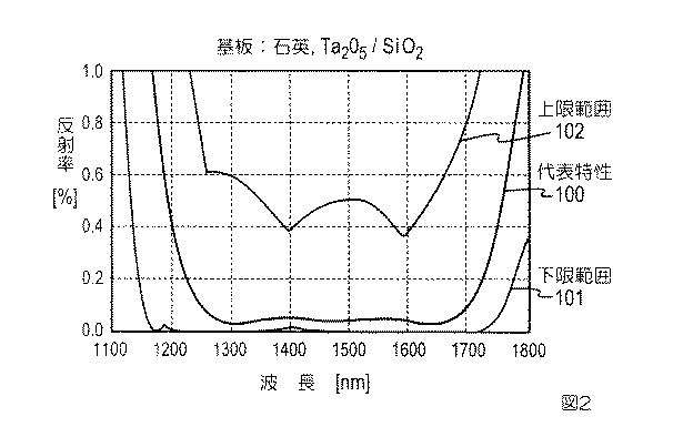
図2は、表2及び表3に例示した膜構成の反射防止膜10の反射防止特性を示した図である。
この図において横軸は波長(nm)を表しており、この例では1100nm〜1800nmの範囲が示されている。また、縦軸は入射光30の反射防止膜10での反射率(%)を表しており、この例では、0.0%〜1.0%の範囲が示されている(後述する図3においても同様)。
また、代表特性100は、表3に例示した膜構成での反射防止特性を示し、上限範囲102は、表2に例示した範囲内で、各光学的膜厚(ndk)を変動させた場合における、各波長の反射防止特性最悪値を、下限範囲101は、その最良値を、それぞれ示したものである。
図2に例示するように、この構成では、波長帯域幅300nmにおいて、反射率0.6%以下の反射防止特性を得ることができ、また、最適化を行うことにより、同条件下、反射率0.1%以下、リップル±0.01%以下の反射防止特性を得ることができる。
【0014】
実施例2
この実施例では、中心周波数λ=1500nmとし、低屈折率膜材料としてSiO2を用い、高屈折率膜材料としてTiO2を用いる。なお、λ=1500nmにおけるTiO2の屈折率は2.173となる。表4に、この実施例における膜構成を示し、表5に、この実施例において各光学的膜厚(ndk)を最適化した膜構成を例示する。
【表4】
図3は、表4及び表5に例示した膜構成の反射防止膜10の反射防止特性を示した図である。なお、この図における代表特性110、上限範囲112及び下限範囲111の意味は、図2の場合と同様である。
図3に例示するように、この構成では、波長帯域幅300nmにおいて、反射率0.7%以下の反射防止特性を得ることができ、また、最適化を行うことにより、同条件下、反射率0.1%以下、リップル±0.01%以下の反射防止特性を得ることができる。
【0016】
なお、この形態の反射防止膜10の用途に特に限定はないが、例えば、波長1.3μ帯や1.5μm帯が用いられる通信機器や、1.6μm帯が用いられる赤外線監視機器等に使用することができる。具体的には、例えば、光カップラ、光ファイバ、光トランシーバ等と入射・出射面等に使用することができる。
また、この形態では低屈折率膜と高屈折率膜を9層積層することとしたが、10層以上の低屈折率膜・高屈折率膜を積層することとしてもよい。ただし、積層数を増加させた場合、これらの膜による光が吸収量が増加し、ロスが大きくなるため、その点を考慮する必要がある。
【0017】
【発明の効果】
以上説明したようにこの発明では、反射防止帯域の設計中心波長λに対する屈折率n1が1.4≦n1≦1.5の関係を満たす低屈折率膜と、この中心波長λに対する屈折率n2が1.9≦n2≦2.4の関係を満たす高屈折率膜とを、基板側から入射光側へ、交互に合計9層積層して反射防止膜を成膜することとした。ここで、この反射防止膜の基板側から入射光側へ数えた第1層、第3相、第5層、第7層及び第9層は低屈折率膜であり、第2層、第4層、第6層及び第8層は高屈折率膜である。また、第1層から第9層までの各光学的膜厚nd1、nd2、nd3、nd4、nd5、nd6、nd7、nd8、nd9は、0.355λ≦nd1≦0.385λ、0.014λ≦nd2≦0.016λ、0.069λ≦nd3≦0.081λ、0.218λ≦nd4≦0.232λ、0.181λ≦nd5≦0.188λ、0.020λ≦nd6≦0.026λ、0.077λ≦nd7≦0.080λ、0.117λ≦nd8≦0.124λ、0.158λ≦nd9≦0.167λの関係を満たす。
これにより、反射防止膜の反射防止特性を広帯域化することができる。また、最適化を行うことにより、反射防止特性のリップルを低減させることもできる。
【図面の簡単な説明】
【図1】反射防止膜の構成を例示した断面図。
【図2】表2及び表3に例示した膜構成の反射防止膜の反射防止特性を示した図。
【図3】表4及び表5に例示した膜構成の反射防止膜の反射防止特性を示した図。
【符号の説明】
10 反射防止膜
11a〜11e 低屈折率膜
12a〜12d 高屈折率膜[0001]
TECHNICAL FIELD OF THE INVENTION
The present invention relates to an antireflection film for preventing reflection of incident light, and more particularly to an antireflection film for preventing reflection of light in a wide wavelength band in a near infrared region.
[0002]
[Prior art]
When light propagates through two media having different refractive indices, a part of the light incident on the interface (for example, about 4% of the incident light at the boundary between air and glass) is reflected. If the optical component is affected by reflection loss or return light, optimum characteristics may not be obtained.
For this reason, in an optical component widely used at present, an antireflection film (AR coat) is generally formed on a boundary surface of a medium where light enters or exits. Here, the “antireflection film” refers to an optically transparent film that prevents reflection of light on the surface of a substance. Conventionally, a film in which a plurality of films having different refractive indices are stacked from two to four layers is used. Was common.
[0003]
However, the conventional antireflection film has a problem that sufficient antireflection characteristics can be obtained only in a bandwidth of about ± 50 nm with respect to the center wavelength of the wavelength band used.
In particular, in recent years, optical communication networks using the 1.3 μm band and the 1.5 μm band have been widely used, and a wavelength bandwidth of about 100 nm is generally used for these applications. Therefore, the conventional antireflection film has no margin in the antireflection band, and it may not be possible to obtain optimum characteristics depending on a manufacturing error, a use environment, and the like. Further, in the case of an optical component commonly used in a plurality of wavelength bands, the antireflection film used therein is required to have antireflection characteristics in all the wavelength bands used. However, a conventional antireflection film that can obtain sufficient antireflection characteristics only in a bandwidth of about ± 50 nm with respect to the center wavelength cannot be used for such an application at all.
[0004]
On the other hand,
[0005]
[Patent Document 1]
JP 10-186104 A
[Problems to be solved by the invention]
However, the antireflection film of
That is, the antireflection film of
The present invention has been made in view of the above points, and provides an antireflection film capable of obtaining antireflection characteristics in a wide band and reducing ripples in the antireflection characteristics in this wide band. The purpose is to:
[0007]
[Means for Solving the Problems]
In order to solve the above problems in the present invention, a low refractive index film having a refractive index n 1 satisfies the relationship of 1.4 ≦ n 1 ≦ 1.5 with respect to the designed center wavelength λ of the antireflection band, for the center wavelength λ a high refractive index film refractive index n 2 is to satisfy the relation of 1.9 ≦ n 2 ≦ 2.4, from the substrate side to the incident light side, an anti-reflection film is provided which is formed by a total of 9 layers stacked alternately . Here, the first layer, the third phase, the fifth layer, the seventh layer, and the ninth layer of the antireflection film counted from the substrate side to the incident light side are low refractive index films, and the second layer, the fourth layer, and the fourth layer. The layers, the sixth layer and the eighth layer are high refractive index films. The optical thicknesses nd 1 , nd 2 , nd 3 , nd 4 , nd 5 , nd 6 , nd 7 , nd 8 , and nd 9 of the first to ninth layers are 0.355λ ≦ nd1 ≦ 0.385λ, 0.014λ ≦ nd2 ≦ 0.016λ, 0.069λ ≦ nd3 ≦ 0.081λ, 0.218λ ≦ nd4 ≦ 0.232λ, 0.181λ ≦ nd5 ≦ 0.188λ, 0.020λ ≦ nd6 ≦ 0.026λ, 0.077λ ≦ nd7 ≦ 0.080λ, 0.117λ ≦ nd8 ≦ 0.124λ, and 0.158λ ≦ nd9 ≦ 0.167λ are satisfied.
[0008]
As a result, at the design center frequency λ = 1.5 μm and the wavelength bandwidth of 300 nm, it is possible to obtain an anti-reflection characteristic with a reflectance of 0.7% or less. Antireflection characteristics of 0.1% or less and ripple ± 0.01% or less can be obtained.
Preferably, the antireflection film of the present invention is formed by alternately laminating a total of nine layers of a SiO 2 film and a Ta 2 O 5 film from the substrate side to the incident light side, and from the substrate side to the incident light side. The counted first, third, fifth, seventh and ninth layers are SiO 2 films, and the second, fourth, sixth and eighth layers are Ta 2 O 5 films. The design center wavelength of the antireflection band is λ, and the optical thicknesses of the first to ninth layers are nd 1 , nd 2 , nd 3 , nd 4 , nd 5 , nd 6 , nd 7 , When nd 8 and nd 9 , 0.355λ ≦ nd1 ≦ 0.385λ, 0.014λ ≦ nd2 ≦ 0.017λ, 0.067λ ≦ nd3 ≦ 0.081λ, 0.215λ ≦ nd4 ≦ 0.232λ, 0.181λ ≦ nd5 ≦ 0.196λ, 0.019λ ≦ nd6 ≦ 0.026λ, 0.077λ ≦ nd7 0.083λ, 0.117λ ≦ nd8 ≦ 0.127λ, satisfy the relationship of 0.154λ ≦ nd9 ≦ 0.167λ.
[0009]
More preferably, the antireflection film of the present invention is formed by alternately stacking a total of nine layers of a SiO 2 film and a TiO 2 film from the substrate side to the incident light side, and counted from the substrate side to the incident light side. The first, third, fifth, seventh, and ninth layers are SiO 2 films, and the second, fourth, sixth, and eighth layers are TiO 2 films. The design center wavelength of the band is λ, and the optical thicknesses of the first to ninth layers are nd 1 , nd 2 , nd 3 , nd 4 , nd 5 , nd 6 , nd 7 , nd 8 , nd In the case of 9 , 0.355λ ≦ nd1 ≦ 0.401λ, 0.014λ ≦ nd2 ≦ 0.016λ, 0.069λ ≦ nd3 ≦ 0.081λ, 0.218λ ≦ nd4 ≦ 0.236λ, 0.174λ ≦ nd5 ≦ 0.188λ, 0.020λ ≦ nd6 ≦ 0.026λ, 0.074λ ≦ nd7 ≦ 0. 080λ, 0.114λ ≦ nd8 ≦ 0.124λ, and 0.158λ ≦ nd9 ≦ 0.171λ.
In the present invention, preferably, the design center wavelength λ satisfies the relationship of 1 μm ≦ λ ≦ 1.7 μm.
[0010]
BEST MODE FOR CARRYING OUT THE INVENTION
Hereinafter, embodiments of the present invention will be described with reference to the drawings. Note that the present invention is not limited to the following embodiments and examples.
FIG. 1 is a cross-sectional view illustrating the configuration of the
As illustrated in FIG. 1, the
[0011]
There is no particular limitation on the method of forming each layer. For example, if an ion beam sputtering (IBM) method is used, the material of each layer can be formed at a high density. It is preferable in that it can be obtained.
Table 1 exemplifies the relationship between the material of each layer and the optical thicknesses (nd k ) of the first to ninth layers. In the example of this table, the optical thicknesses (nd k ) from the first layer to the ninth layer are sequentially denoted by nd 1 , nd 2 , nd 3 , nd 4 , nd 5 , nd 6 , nd 7 , nd 8 , nd 9 and the center wavelength λ is 1 μm ≦ λ ≦ 1.7 μm.
[Table 1]
Hereinafter, examples of this embodiment will be described.
[0012]
Example 1
In this embodiment, center frequency λ = 1500 nm, SiO 2 is used as a low refractive index film material, and Ta 2 O 5 is used as a high refractive index film material. The refractive index of SiO 2 at λ = 1500 nm is 1.467, and the refractive index of Ta 2 O 5 is 2.063. Table 2 shows a film configuration in this example, and Table 3 exemplifies a film configuration in which each optical film thickness (nd k ) is optimized in this example.
[Table 2]
FIG. 2 is a diagram showing the antireflection characteristics of the
In this figure, the horizontal axis represents the wavelength (nm), and in this example, the range from 1100 nm to 1800 nm is shown. The vertical axis represents the reflectance (%) of the
Further, the representative characteristic 100 indicates the anti-reflection characteristic in the film configuration exemplified in Table 3, and the
As illustrated in FIG. 2, in this configuration, it is possible to obtain an anti-reflection characteristic with a reflectance of 0.6% or less in a wavelength bandwidth of 300 nm, and to optimize the reflectance under the same conditions by optimization. Antireflection characteristics of 0.1% or less and ripple ± 0.01% or less can be obtained.
[0014]
Example 2
In this embodiment, the center frequency λ is 1500 nm, SiO 2 is used as the low refractive index film material, and TiO 2 is used as the high refractive index film material. The refractive index of TiO2 at λ = 1500 nm is 2.173. Table 4 shows a film configuration in this example, and Table 5 exemplifies a film configuration in which each optical film thickness (nd k ) is optimized in this example.
[Table 4]
FIG. 3 is a diagram showing the antireflection characteristics of the
As exemplified in FIG. 3, in this configuration, it is possible to obtain an anti-reflection characteristic with a reflectance of 0.7% or less in a wavelength bandwidth of 300 nm. Antireflection characteristics of 0.1% or less and ripple ± 0.01% or less can be obtained.
[0016]
The application of the
In this embodiment, nine low-refractive-index films and nine high-refractive-index films are stacked, but ten or more low-refractive-index films and high-refractive-index films may be stacked. However, when the number of layers is increased, the amount of light absorbed by these films is increased, and the loss is increased.
[0017]
【The invention's effect】
In the above the invention as described, and a low refractive index film having a refractive index n 1 satisfies the relationship of 1.4 ≦ n 1 ≦ 1.5 with respect to the designed center wavelength λ of the antireflection band, the refractive index with respect to the central wavelength λ n 2 is a high refractive index film which satisfies a relation of 1.9 ≦ n 2 ≦ 2.4, from the substrate side to the incident light side, it was decided to deposit the anti-reflection film by alternately nine layer laminate . Here, the first layer, the third phase, the fifth layer, the seventh layer, and the ninth layer of the antireflection film counted from the substrate side to the incident light side are low refractive index films, and the second layer, the fourth layer, and the fourth layer. The layers, the sixth layer and the eighth layer are high refractive index films. The optical thicknesses nd 1 , nd 2 , nd 3 , nd 4 , nd 5 , nd 6 , nd 7 , nd 8 , and nd 9 of the first to ninth layers are 0.355λ ≦ nd1 ≦ 0.385λ, 0.014λ ≦ nd2 ≦ 0.016λ, 0.069λ ≦ nd3 ≦ 0.081λ, 0.218λ ≦ nd4 ≦ 0.232λ, 0.181λ ≦ nd5 ≦ 0.188λ, 0.020λ ≦ nd6 ≦ 0.026λ, 0.077λ ≦ nd7 ≦ 0.080λ, 0.117λ ≦ nd8 ≦ 0.124λ, and 0.158λ ≦ nd9 ≦ 0.167λ are satisfied.
Thereby, the antireflection characteristic of the antireflection film can be broadened. Further, by performing the optimization, the ripple of the antireflection characteristic can be reduced.
[Brief description of the drawings]
FIG. 1 is a cross-sectional view illustrating the configuration of an antireflection film.
FIG. 2 is a view showing the antireflection characteristics of antireflection films having the film configurations exemplified in Tables 2 and 3.
FIG. 3 is a diagram showing the antireflection characteristics of the antireflection films having the film configurations exemplified in Tables 4 and 5.
[Explanation of symbols]
10 Antireflection films 11a to 11e Low refractive index films 12a to 12d High refractive index films
Claims (4)
反射防止帯域の設計中心波長λに対する屈折率n1が1.4≦n1≦1.5の関係を満たす低屈折率膜と、この中心波長λに対する屈折率n2が1.9≦n2≦2.4の関係を満たす高屈折率膜とを、前記基板側から入射光側へ、交互に合計9層積層してなり、
前記基板側から前記入射光側へ数えた第1層、第3相、第5層、第7層及び第9層は前記低屈折率膜であり、第2層、第4層、第6層及び第8層は前記高屈折率膜であり、
前記第1層から前記第9層までの各光学的膜厚を順にnd1、nd2、nd3、nd4、nd5、nd6、nd7、nd8、nd9とした場合に、
0.355λ≦nd1≦0.385λ、
0.014λ≦nd2≦0.016λ、
0.069λ≦nd3≦0.081λ、
0.218λ≦nd4≦0.232λ、
0.181λ≦nd5≦0.188λ、
0.020λ≦nd6≦0.026λ、
0.077λ≦nd7≦0.080λ、
0.117λ≦nd8≦0.124λ、
0.158λ≦nd9≦0.167λ、
の関係を満たすことを特徴とする反射防止膜。An anti-reflection film laminated on the substrate and preventing reflection of light incident on the substrate surface,
And a low refractive index film having a refractive index n 1 with respect to the designed center wavelength λ of the antireflection band satisfies the relation of 1.4 ≦ n 1 ≦ 1.5, the refractive index n 2 with respect to the center wavelength λ is 1.9 ≦ n 2 A high-refractive-index film satisfying a relationship of ≦ 2.4, and a total of nine layers are alternately laminated from the substrate side to the incident light side;
The first, third, fifth, seventh, and ninth layers counted from the substrate side to the incident light side are the low-refractive-index films, and are the second, fourth, and sixth layers. And the eighth layer is the high refractive index film,
When the respective optical thicknesses from the first layer to the ninth layer are nd 1 , nd 2 , nd 3 , nd 4 , nd 5 , nd 6 , nd 7 , nd 8 , and nd 9 ,
0.355λ ≦ nd1 ≦ 0.385λ,
0.014λ ≦ nd2 ≦ 0.016λ,
0.069λ ≦ nd3 ≦ 0.081λ,
0.218λ ≦ nd4 ≦ 0.232λ,
0.181λ ≦ nd5 ≦ 0.188λ,
0.020λ ≦ nd6 ≦ 0.026λ,
0.077λ ≦ nd7 ≦ 0.080λ,
0.117λ ≦ nd8 ≦ 0.124λ,
0.158λ ≦ nd9 ≦ 0.167λ,
An anti-reflection film characterized by satisfying the following relationship:
SiO2膜とTa2O5膜とを、前記基板側から入射光側へ、交互に合計9層積層してなり、
前記基板側から前記入射光側へ数えた第1層、第3相、第5層、第7層及び第9層はSiO2膜であり、第2層、第4層、第6層及び第8層はTa2O5膜であり、
反射防止帯域の設計中心波長をλとし、前記第1層から前記第9層までの各光学的膜厚を順にnd1、nd2、nd3、nd4、nd5、nd6、nd7、nd8、nd9とした場合に、
0.355λ≦nd1≦0.385λ、
0.014λ≦nd2≦0.017λ、
0.067λ≦nd3≦0.081λ、
0.215λ≦nd4≦0.232λ、
0.181λ≦nd5≦0.196λ、
0.019λ≦nd6≦0.026λ、
0.077λ≦nd7≦0.083λ、
0.117λ≦nd8≦0.127λ、
0.154λ≦nd9≦0.167λ、
の関係を満たすことを特徴とする反射防止膜。An anti-reflection film laminated on the substrate and preventing reflection of light incident on the substrate surface,
A total of nine layers of SiO 2 films and Ta 2 O 5 films are alternately laminated from the substrate side to the incident light side,
The first layer, the third phase, the fifth layer, the seventh layer, and the ninth layer counted from the substrate side to the incident light side are SiO 2 films, and the second layer, the fourth layer, the sixth layer, and the Eight layers are Ta 2 O 5 films,
The design center wavelength of the antireflection band is λ, and the optical thicknesses from the first layer to the ninth layer are nd 1 , nd 2 , nd 3 , nd 4 , nd 5 , nd 6 , nd 7 , When nd 8 and nd 9 are set,
0.355λ ≦ nd1 ≦ 0.385λ,
0.014λ ≦ nd2 ≦ 0.017λ,
0.067λ ≦ nd3 ≦ 0.081λ,
0.215λ ≦ nd4 ≦ 0.232λ,
0.181λ ≦ nd5 ≦ 0.196λ,
0.019λ ≦ nd6 ≦ 0.026λ,
0.077λ ≦ nd7 ≦ 0.083λ,
0.117λ ≦ nd8 ≦ 0.127λ,
0.154λ ≦ nd9 ≦ 0.167λ,
An anti-reflection film characterized by satisfying the following relationship:
SiO2膜とTiO2膜とを、前記基板側から入射光側へ、交互に合計9層積層してなり、
前記基板側から前記入射光側へ数えた第1層、第3相、第5層、第7層及び第9層はSiO2膜であり、第2層、第4層、第6層及び第8層はTiO2膜であり、
反射防止帯域の設計中心波長をλとし、前記第1層から前記第9層までの各光学的膜厚を順にnd1、nd2、nd3、nd4、nd5、nd6、nd7、nd8、nd9とした場合に、
0.355λ≦nd1≦0.401λ、
0.014λ≦nd2≦0.016λ、
0.069λ≦nd3≦0.081λ、
0.218λ≦nd4≦0.236λ、
0.174λ≦nd5≦0.188λ、
0.020λ≦nd6≦0.026λ、
0.074λ≦nd7≦0.080λ、
0.114λ≦nd8≦0.124λ、
0.158λ≦nd9≦0.171λ、
の関係を満たすことを特徴とする反射防止膜。An anti-reflection film laminated on the substrate and preventing reflection of light incident on the substrate surface,
A total of nine layers of SiO 2 films and TiO 2 films are alternately laminated from the substrate side to the incident light side,
The first layer, the third phase, the fifth layer, the seventh layer, and the ninth layer counted from the substrate side to the incident light side are SiO 2 films, and the second layer, the fourth layer, the sixth layer, and the Eight layers are TiO 2 films,
The design center wavelength of the antireflection band is λ, and the optical thicknesses from the first layer to the ninth layer are nd 1 , nd 2 , nd 3 , nd 4 , nd 5 , nd 6 , nd 7 , When nd 8 and nd 9 are set,
0.355λ ≦ nd1 ≦ 0.401λ,
0.014λ ≦ nd2 ≦ 0.016λ,
0.069λ ≦ nd3 ≦ 0.081λ,
0.218λ ≦ nd4 ≦ 0.236λ,
0.174λ ≦ nd5 ≦ 0.188λ,
0.020λ ≦ nd6 ≦ 0.026λ,
0.074λ ≦ nd7 ≦ 0.080λ,
0.114λ ≦ nd8 ≦ 0.124λ,
0.158λ ≦ nd9 ≦ 0.171λ,
An anti-reflection film characterized by satisfying the following relationship:
Priority Applications (1)
| Application Number | Priority Date | Filing Date | Title |
|---|---|---|---|
| JP2003087864A JP3741692B2 (en) | 2003-03-27 | 2003-03-27 | Anti-reflection coating |
Applications Claiming Priority (1)
| Application Number | Priority Date | Filing Date | Title |
|---|---|---|---|
| JP2003087864A JP3741692B2 (en) | 2003-03-27 | 2003-03-27 | Anti-reflection coating |
Publications (2)
| Publication Number | Publication Date |
|---|---|
| JP2004294841A true JP2004294841A (en) | 2004-10-21 |
| JP3741692B2 JP3741692B2 (en) | 2006-02-01 |
Family
ID=33402150
Family Applications (1)
| Application Number | Title | Priority Date | Filing Date |
|---|---|---|---|
| JP2003087864A Expired - Fee Related JP3741692B2 (en) | 2003-03-27 | 2003-03-27 | Anti-reflection coating |
Country Status (1)
| Country | Link |
|---|---|
| JP (1) | JP3741692B2 (en) |
Cited By (3)
| Publication number | Priority date | Publication date | Assignee | Title |
|---|---|---|---|---|
| JP2014164120A (en) * | 2013-02-25 | 2014-09-08 | Olympus Corp | Antireflection film, optical system, and optical equipment |
| CN106946470A (en) * | 2017-04-26 | 2017-07-14 | 福建福光光电科技有限公司 | The day and night two optometry glass film that a kind of corrosion-resistant height is anti-reflection |
| US9709705B2 (en) | 2013-07-03 | 2017-07-18 | Canon Kabushiki Kaisha | Anti-reflection film and optical element having the same |
-
2003
- 2003-03-27 JP JP2003087864A patent/JP3741692B2/en not_active Expired - Fee Related
Cited By (3)
| Publication number | Priority date | Publication date | Assignee | Title |
|---|---|---|---|---|
| JP2014164120A (en) * | 2013-02-25 | 2014-09-08 | Olympus Corp | Antireflection film, optical system, and optical equipment |
| US9709705B2 (en) | 2013-07-03 | 2017-07-18 | Canon Kabushiki Kaisha | Anti-reflection film and optical element having the same |
| CN106946470A (en) * | 2017-04-26 | 2017-07-14 | 福建福光光电科技有限公司 | The day and night two optometry glass film that a kind of corrosion-resistant height is anti-reflection |
Also Published As
| Publication number | Publication date |
|---|---|
| JP3741692B2 (en) | 2006-02-01 |
Similar Documents
| Publication | Publication Date | Title |
|---|---|---|
| JP5774807B2 (en) | Narrow-band omnidirectional reflectors and their use as structural colors | |
| JP3332879B2 (en) | Dichroic mirror | |
| JP6202785B2 (en) | Antireflection film, optical system, optical apparatus, and method for forming antireflection film | |
| JP6449999B2 (en) | Antireflection film, optical element and optical system | |
| WO2013105210A1 (en) | Optical multilayer film | |
| JP3290629B2 (en) | Optical multilayer filter | |
| WO2005116696A1 (en) | Reflection preventing film | |
| JP2007183525A (en) | Dielectric multilayer film filter | |
| JP2012255984A (en) | Antireflection film, optical system and optical apparatus | |
| JP2007171735A (en) | Wide band anti-reflection film | |
| JP2009156954A (en) | Wavelength separation film, and optical communication filter using the same | |
| JP3741692B2 (en) | Anti-reflection coating | |
| JP3373182B2 (en) | Multilayer optical filter | |
| CN110737099B (en) | Polarization independent beam splitter | |
| JPH0875902A (en) | Multilayer reflection preventing film | |
| US8934172B2 (en) | Mirror | |
| JP2003043245A (en) | Optical filter | |
| JP6108871B2 (en) | Antireflection film, optical system, and optical apparatus | |
| JP2004258494A (en) | Nd filter | |
| JP2013068885A (en) | Bandpass filter, and method of manufacturing bandpass filter | |
| WO2022052268A1 (en) | Lens and lens assembly | |
| CN212515112U (en) | Optical filter for high-speed transmission and optical module | |
| JP3550894B2 (en) | Anti-reflective coating | |
| JP2005004022A (en) | Antireflection coating | |
| CN212658849U (en) | Optical filter and optical module for 5G network DWDM system |
Legal Events
| Date | Code | Title | Description |
|---|---|---|---|
| A977 | Report on retrieval |
Free format text: JAPANESE INTERMEDIATE CODE: A971007 Effective date: 20050930 |
|
| TRDD | Decision of grant or rejection written | ||
| A01 | Written decision to grant a patent or to grant a registration (utility model) |
Free format text: JAPANESE INTERMEDIATE CODE: A01 Effective date: 20051018 |
|
| A61 | First payment of annual fees (during grant procedure) |
Free format text: JAPANESE INTERMEDIATE CODE: A61 Effective date: 20051108 |
|
| R150 | Certificate of patent or registration of utility model |
Free format text: JAPANESE INTERMEDIATE CODE: R150 |
|
| LAPS | Cancellation because of no payment of annual fees |