JP2004282081A - Method of integrating thin film resistor into dual damascene structure - Google Patents
Method of integrating thin film resistor into dual damascene structure Download PDFInfo
- Publication number
- JP2004282081A JP2004282081A JP2004073661A JP2004073661A JP2004282081A JP 2004282081 A JP2004282081 A JP 2004282081A JP 2004073661 A JP2004073661 A JP 2004073661A JP 2004073661 A JP2004073661 A JP 2004073661A JP 2004282081 A JP2004282081 A JP 2004282081A
- Authority
- JP
- Japan
- Prior art keywords
- thin film
- film resistor
- dielectric layer
- forming
- layer
- Prior art date
- Legal status (The legal status is an assumption and is not a legal conclusion. Google has not performed a legal analysis and makes no representation as to the accuracy of the status listed.)
- Pending
Links
Images


Classifications
-
- H—ELECTRICITY
- H01—ELECTRIC ELEMENTS
- H01L—SEMICONDUCTOR DEVICES NOT COVERED BY CLASS H10
- H01L28/00—Passive two-terminal components without a potential-jump or surface barrier for integrated circuits; Details thereof; Multistep manufacturing processes therefor
- H01L28/20—Resistors
-
- H—ELECTRICITY
- H01—ELECTRIC ELEMENTS
- H01L—SEMICONDUCTOR DEVICES NOT COVERED BY CLASS H10
- H01L21/00—Processes or apparatus adapted for the manufacture or treatment of semiconductor or solid state devices or of parts thereof
- H01L21/70—Manufacture or treatment of devices consisting of a plurality of solid state components formed in or on a common substrate or of parts thereof; Manufacture of integrated circuit devices or of parts thereof
- H01L21/71—Manufacture of specific parts of devices defined in group H01L21/70
- H01L21/768—Applying interconnections to be used for carrying current between separate components within a device comprising conductors and dielectrics
-
- H—ELECTRICITY
- H01—ELECTRIC ELEMENTS
- H01L—SEMICONDUCTOR DEVICES NOT COVERED BY CLASS H10
- H01L23/00—Details of semiconductor or other solid state devices
- H01L23/52—Arrangements for conducting electric current within the device in operation from one component to another, i.e. interconnections, e.g. wires, lead frames
- H01L23/522—Arrangements for conducting electric current within the device in operation from one component to another, i.e. interconnections, e.g. wires, lead frames including external interconnections consisting of a multilayer structure of conductive and insulating layers inseparably formed on the semiconductor body
- H01L23/5228—Resistive arrangements or effects of, or between, wiring layers
-
- H—ELECTRICITY
- H01—ELECTRIC ELEMENTS
- H01L—SEMICONDUCTOR DEVICES NOT COVERED BY CLASS H10
- H01L2924/00—Indexing scheme for arrangements or methods for connecting or disconnecting semiconductor or solid-state bodies as covered by H01L24/00
- H01L2924/0001—Technical content checked by a classifier
- H01L2924/0002—Not covered by any one of groups H01L24/00, H01L24/00 and H01L2224/00
Abstract
Description
本発明は一般的に薄膜レジスターの分野に関し、より詳細には銅インターコネクトにより二重ダマシン構造内に薄膜レジスターを形成する方法に関する。 The present invention relates generally to the field of thin film resistors, and more particularly, to a method of forming a thin film resistor in a dual damascene structure with a copper interconnect.
発明の背景
薄膜レジスターは高精度のアナログおよび混合シグナルのアプリケーションのための非常に魅力的な部品である。抵抗の熱係数が低いことの他に、抵抗の電圧係数が低いこととレジスターのマッチングが優れていることにより、これらはストレス下で優れた安定性を示す筈である。
BACKGROUND OF THE INVENTION Thin film resistors are very attractive components for precision analog and mixed signal applications. Due to the low thermal coefficient of the resistors, as well as the low voltage coefficient of the resistors and the excellent matching of the resistors, they should exhibit good stability under stress.
高周波混合シグナルのアプリケーションには銅インターコネクトの使用が必要である。集積回路のための銅インターコネクトはダマシン・プロセスにより形成される。同プロセスでは、最初にトレンチを誘電層内に形成する。次いで、銅を同トレンチ内に満たし、余剰の銅は各種の方法(例えば化学機械的なポリッシング)により除去される。 High frequency mixed signal applications require the use of copper interconnects. Copper interconnects for integrated circuits are formed by a damascene process. In the process, a trench is first formed in a dielectric layer. Next, copper is filled in the trench, and excess copper is removed by various methods (for example, chemical mechanical polishing).
銅インターコネクトを含む集積回路内に薄膜レジスターを形成するためには多くの困難がつきまとう。薄膜レジスターは銅を使用して形成するわけではないので、既存のダマシン・プロセスによる形成は適切ではない。薄膜レジスターは銅インターコネクトと同一の高さで形成する必要があるので、同プロセスの不適切さは更に増すことになる。従って、ダマシン・プロセスにより形成された銅インターコネクトを使用して集積回路内に薄膜レジスターを形成する方法が必要である。 There are many difficulties associated with forming thin film resistors in integrated circuits that include copper interconnects. Since thin film resistors are not formed using copper, formation by existing damascene processes is not appropriate. Because the thin film resistors must be formed at the same height as the copper interconnect, the inadequacy of the process is further increased. Therefore, there is a need for a method of forming a thin film resistor in an integrated circuit using a copper interconnect formed by a damascene process.
発明の要約
本発明は、二重ダマシン構造を使用して形成された銅インターコネクトを含む集積回路内に薄膜レジスターを組み入れる方法に関する。本発明のひとつの実施態様においては、誘電層をエッチング停止層上に形成する。薄膜レジスターをエッチング停止層の上側に形成し、更に導体パッドを薄膜レジスター上に形成する。第二の誘電層を薄膜レジスターの上側に形成し、同第二の誘電層内に少なくとも1個のトレンチを形成する。それと同時に、薄膜レジスター上の導体パッドの上側に薄膜レジスターのためのバイア(vias)を形成する。トレンチ構造内に1個のバイアトレンチを形成し、トレンチ、バイアトレンチおよび薄膜レジスターの複数のバイア内に金属を満たす(formed:形成する)。
同様の特徴を説明する図全体にわたって共通の符号が用いられている。
これらの図は縮尺どおりに描かれているのではなく、単なる説明のための目的で描かれている。
SUMMARY OF THE INVENTION The present invention relates to a method of incorporating a thin film resistor in an integrated circuit including a copper interconnect formed using a dual damascene structure. In one embodiment of the present invention, a dielectric layer is formed on the etch stop layer. A thin film resistor is formed above the etch stop layer, and a contact pad is formed on the thin film resistor. A second dielectric layer is formed over the thin-film resistor, and at least one trench is formed in the second dielectric layer. At the same time, a via for the thin film resistor is formed above the conductive pad on the thin film resistor. A via trench is formed in the trench structure and metal is formed in the vias of the trench, via trench and thin film resistor.
Common reference numerals are used throughout the figures to describe similar features.
These figures are not drawn to scale, but are drawn for illustrative purposes only.
発明の詳細な説明
以下において本発明を図1〜2を参照して説明するが、本発明は多くの半導体装置構造のために使用可能である。本発明の方法論により、銅インターコネクトを含む集積回路内に薄膜レジスターを形成するための解決策が提供される。
DETAILED DESCRIPTION OF THE INVENTION In the following, the present invention is described with reference to FIGS. 1-2, but the present invention can be used for many semiconductor device structures. The methodology of the present invention provides a solution for forming a thin film resistor in an integrated circuit that includes a copper interconnect.
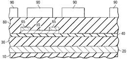
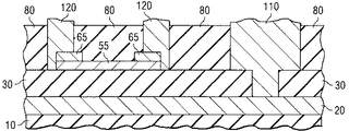
図1(a)〜1(f)に本発明の一実施態様を説明している。図1(a)に示すように、金属製インターコネクト20は誘電層10の上側に形成される。誘電層10は半導体基板および介在する層(その数は指定されない)の上側に形成される。簡便のために、半導体基板および介在する層(その数は指定されない)はこれらの図には示されていない。これらの図には示されていないが、誘電層10の下側には実際の働きをする層(例えば、MOSおよび/あるいはバイポーラートランジスター、その数は指定されない)や金属製インターコネクト層(その数は指定されない)が存在するであろう。図1(a)に示すように、中間層としての誘電層30を金属製インターコネクト20の上側に形成する。中間層としての誘電層30は化学蒸着のような適切な方法(その種類は問わない)で形成された酸化ケイ素を含んでいてもよい。第一の実施態様においては、中間層としての誘電層30は、TEOS酸化ケイ素、PECVD酸化ケイ素、窒化ケイ素、酸窒化ケイ素、炭化ケイ素、スピンオングラス(SOG、例えば、シルセスキオキサンおよびシロキサン)、乾膠体(xerogels:キセロゲル)、その他の全ての適切な材料からなる群より選ばれる材料を用いて形成する。中間層としての誘電層30を形成した後、エッチング停止層40を同の誘電層30の上側に形成する。本発明の一実施態様においては、エッチング停止層40は窒化ケイ素、炭化ケイ素、酸窒化ケイ素、これらのひとつあるいは全てとその他の適切な層の組み合わせ、および種類を問わずその他の適切な誘電材料を含んでよい。次いで、薄膜レジスター層50をエッチング停止層40の上側に形成する。それに続く処理において、薄膜レジスター層50をエッチング処理して薄膜レジスター(TFR)が形成されよう。本発明の一実施態様においては、薄膜レジスター層50を形成する材料はシリコン/クロム(SiCr)合金、ニッケル/クロム(NiCr)合金、窒化タンタル、窒化チタン、タングステンその他の適切などのような材料でもよい。フォトレジスト層58を薄膜レジスター層50の上側に形成してパターン化する。これは、エッチング工程中でTFRを特徴付けるために使用されることになろう。
1 (a) to 1 (f) illustrate one embodiment of the present invention. As shown in FIG. 1A, a
図1(b)に薄膜レジスター層50の上側に形成したTFR55を示している。これは図1(a)に示すフォトレジスト層58をマスキング層として使用してエッチングにより形成した。薄膜レジスター層50はいかなる適切なドライあるいはウエット・エッチングによりエッチングできる。TFR構造55の形成後、導電性の導体層60をTFR構造55の上側に形成する。本発明の一実施態様においては、導電性の導体層(contact layer:接触層)60を形成する材料は窒化チタン、窒化タングステン、その他の適切などのような導電性材料でもよい。本発明の別の実施態様においては、導電性の導体層60は同じあるいは異なった種類の導電性材料による多層構造であってもよい。導体層60の形成後、パターン化されたフォトレジスト層70をキャッピング層の上側に形成する(図1(b)を参照)。これはその後導体層60のパターニングのために使用されることになろう。
FIG. 1B shows the
図1(b)に示す導体層60のエッチングが完了後、導体パッド65を形成する(図1(c)を参照)。導体パッド65は続いて実施されるトレンチのエッチング中にTFR55を保護することになろう。導体パッド65の形成後、中間層としての誘電層80をTFR55の上側に形成する。中間層としての誘電層80は化学蒸着のような適切な方法(その種類は問わない)で形成された酸化ケイ素を含んでいてもよい。本発明の一実施態様においては、中間層としての誘電層80は、TEOS酸化ケイ素、PECVD酸化ケイ素、窒化ケイ素、酸窒化ケイ素、炭化ケイ素、スピンオングラス(SOG、例えば、シルセスキオキサンおよびシロキサン)、乾膠体、その他の全ての適切な材料からなる群より選ばれる材料を用いて形成する。中間層としての誘電層80を形成した後、パターン化されたフォトレジスト層90を誘電層80の上側に形成する。パターン化されたフォトレジスト層90は続いて実施される誘電層80内のバイアおよびトレンチのエッチング中にマスクの役割を果たすことになろう。
After the etching of the
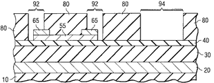
図1(d)に、図1(c)に示す構造において中間層としての誘電層80内のTFRバイア92(複数)およびトレンチ94を同時にエッチングした後の構造を示している。同図ではTFRおよびトレンチを各々1個しか示していないが、本発明の方法では複数のTFRバイアの他に、誘電層内にトレンチ構造およびバイア構造をいかなる数でも形成するために使用できることに注意されたい。また、バイアは本発明において、その下側にある導電性層(例えば、TFRあるいは金属製インターコネクト)あるいは電子装置と接触する構造を説明する際に用いられること、またトレンチはその中に金属製インターコネクト線が形成される誘電層内に形成される構造体を説明する際に用いられることにも注意されたい。
FIG. 1D shows the structure after the
図1(d)に示す中間層としての誘電層80のエッチングは、エッチング停止層40の所でエッチングを停止するように設計されたドライエッチング・プロセスによって実施する。誘電層80が酸化ケイ素製でありエッチング停止層40が窒化ケイ素製の場合には、窒化ケイ素に対する酸化ケイ素の選択性が高いどのようなドライエッチング・プロセスでも使用できる。誘電層80のエッチング工程中では、導体パッド65はエッチング・プロセスに曝された可能性があるTFR領域を保護するであろうことに注意されたい。従って、使用されるエッチング・プロセスは、誘電層80と導体パッド65の間にも高い選択性を有していなければならない。エッチング処理を受けたTFRバイア92はTFR55に対する電気的接点を提供するために使用されるであろうし、また銅製のインターコネクト金属線はトレンチ構造94内に形成されることになろう。
The etching of the
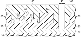
図1(d)に示すトレンチ94およびTFRバイア92の形成後、パターン化されたフォトレジスト層100を形成し、これをトレンチバイア96の形成工程中にマスクとして使用する。トレンチバイア96をエッチング停止層40およびその下側の誘電層30を通過して実施されるエッチングにより形成する。図1(f)に示すように、トレンチバイア96の形成後、フォトレジスト層100を除去し、またメタル120および110を各々TFRバイアとトレンチ内およびトレンチバイア内に形成する。本発明の一実施態様においては、形成される金属は銅でもよいし、それ以外の適切ないかなるものでもよい。銅金属を使用する場合には、それ(120及び110)の形成には集積回路を処理するどのような既知の方法(例えば、銅金属付着および化学機械的なポリッシング)を用いてよい。図1(f)に示す構造の形成後、既知の製造方法により集積回路を完成できる。
After forming the
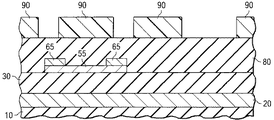
本発明の他の実施態様を図2(a)〜2(d)に示している。図2(a)に誘電層10の上側に形成した金属製インターコネクト20を示している。中間層としての誘電層30を金属製インターコネクト層10の上側に形成する。中間層としての誘電層30は化学蒸着のような適切な方法(その種類は問わない)で形成された酸化ケイ素を含んでいてもよい。第一の実施態様においては、中間層としての誘電層30は、TEOS酸化ケイ素、PECVD酸化ケイ素、窒化ケイ素、酸窒化ケイ素、炭化ケイ素、スピンオングラス(SOG、例えば、シルセスキオキサンおよびシロキサン)、乾膠体、その他の全ての適切な材料からなる群より選ばれる材料を用いて形成する。中間層としての誘電層30を形成した後、薄膜レジスター55および導体パッド65をこの順に形成する。本発明の一実施態様においては、同レジスター層を形成する材料はシリコン/クロム(SiCr)合金、ニッケル/クロム(NiCr)合金、窒化タンタル、窒化チタン、タングステンその他の適切などのような材料でもよい。
Another embodiment of the present invention is shown in FIGS. 2 (a) to 2 (d). FIG. 2A shows a
TFR55と導体パッド65の形成後、導電性の導体層80をTFR55の上側に形成する。中間層としての誘電層80は化学蒸着のような適切な方法(その種類は問わない)で形成された酸化ケイ素を含んでいてもよい。本発明の一実施態様においては、中間層としての誘電層80は、TEOS酸化ケイ素、PECVD酸化ケイ素、窒化ケイ素、酸窒化ケイ素、炭化ケイ素、スピンオングラス(SOG、例えば、シルセスキオキサンおよびシロキサン)、乾膠体、その他の全ての適切な材料からなる群より選ばれる材料を用いて形成する。中間層としての誘電層80を形成した後、パターン化されたフォトレジスト層90を誘電層80の上側に形成する。パターン化されたフォトレジスト層90は続いて実施される誘電層80内のトレンチのエッチング中にマスクの役割を果たすことになろう。
After the formation of the
図2(b)に、図2(a)に示す構造において中間層としての誘電層80内のTFRバイア92(複数)およびトレンチ94を同時にエッチングした後の構造を示している。図2(b)に示す中間層としての誘電層80のエッチングは、誘電層80を通ってエッチング停止層40の所でエッチングを停止するように設計されたプログラム化されたドライエッチング・プロセスによって実施する。エッチングを誘電層80と30の間の界面で厳密に停止することは必須ではない。それでも、エッチング・プロセス完了後には導体パッド(contact pads)65が外面に露出することは重要である。中間層としての誘電層80のエッチング工程中では、導体パッド65はエッチング・プロセスに曝された可能性があるTFR55を保護することになろう。このことは、使用されるエッチング・プロセスは誘電層80と導体パッド65の間にも高い選択性を有していなければならないことを意味する。エッチング処理を受けたTFRバイア92はTFR55に対する電気的接点を提供するために使用されるであろうし、また銅製のインターコネクト金属はトレンチ構造94内に形成されることになろう。
FIG. 2B shows the structure of FIG. 2A after the TFR vias 92 and the
図2(b)に示すトレンチ94およびTFRバイア92の形成後、パターン化されたフォトレジスト層100を形成し、これをトレンチバイア96の形成工程中にマスクとして使用する。トレンチバイア96をエッチング停止層40およびその下側の誘電層30を通過して実施されるエッチングにより形成する。図2(d)に示すように、トレンチバイア96の形成後、フォトレジスト層100を除去し、また銅メタル120および110を各々TFRバイアとトレンチ内およびトレンチバイア内に形成する。銅メタル120および110の形成には集積回路を処理するどのような既知の方法(例えば、銅金属付着および化学機械的なポリッシング)を用いてよい。図2(d)に示す構造の形成後、既知の製造方法により集積回路を完成できる。
After the formation of the
本発明を説明的な実施態様を参照しつつ説明したが、これらの記載事項は本発明を制限するためのものではないと解釈すべきである。当業界での熟練者は本明細書での記載事項を参照すれば、上記の説明的な実施態様およびその他の本発明の実施態様を変更したりそれらを組み合わせることが可能であることは明らかである。従って、添付の特許請求の範囲はそのような変更あるいは実施態様を包含していると解釈される。 Although the invention has been described with reference to illustrative embodiments, these descriptions should not be construed as limiting the invention. It will be apparent to those skilled in the art, having reference to the description herein, that the above illustrative embodiments and other embodiments of the present invention may be modified or combined. is there. It is therefore contemplated that the appended claims will cover such modifications or embodiments.
以上の説明に関して更に以下の項を開示する。
(1)以下の工程を包含する集積回路用薄膜レジスター(thin film resistor)を形成する方法:
第一の誘電層を半導体の上側に形成する;
エッチング停止層(etch stop layer:エッチストッパ層)を上記誘電層上に形成する;
薄膜レジスターを上記エッチング停止層の上側に形成する;
第二の誘電層を上記薄膜レジスターの上側に形成する;
少なくとも1個のトレンチと薄膜レジスターバイア(複数)を上記第二の誘電層内に同時に形成する;
1個のトレンチバイアを上記少なくとも1個のトレンチ内に形成する;および
上記薄膜レジスターバイア、トレンチおよびトレンチバイアを金属で満たす。
(2)上記の第二の誘電層が、TEOS酸化ケイ素、PECVD酸化ケイ素、シルセスキオキサン、シロキサンおよび乾膠体(キセロゲル)からなる群より選ばれる材料を含む、(1)記載の方法。
(3)上記のエッチング停止層が窒化ケイ素を含むことを特徴とする(2)記載の方法。
(4)上記の薄膜レジスターの上に更に導体パッドを形成する第1クレームの方法において、上記薄膜レジスターでのバイアが上記導体パッドの上に位置していることを特徴とする(1)記載の方法。
(5)上記の薄膜レジスターがシリコン/クロム(SiCr)合金、ニッケル/クロム(NiCr)合金、窒化タンタル、窒化チタンおよびタングステンからなる群より選ばれる材料を用いて形成されることを特徴とする(1)記載の方法。
(6)以下の工程から構成されることを特徴とする薄膜レジスターを形成する方法:
第一の誘電層を半導体の上側に形成する;
薄膜レジスターを上記第一の誘電層の上側に形成する;
第二の誘電層を上記薄膜レジスターの上側に形成する;
少なくとも1個のトレンチと薄膜レジスターバイア(複数)を上記第二の誘電層内に同時に形成する;
1個のトレンチバイアを上記少なくとも1個のトレンチ内に形成する;および
上記薄膜レジスターバイア、トレンチおよびトレンチバイアを金属で満たす。
(7)上記の第二の誘電層がTEOS酸化ケイ素、PECVD酸化ケイ素、シルセスキオキサンおよび乾膠体からなる群より選ばれる材料を用いて形成されることを特徴とする(6)記載の方法。
(8)上記の薄膜レジスターの上に更に導体パッドを形成し、上記薄膜レジスターでのバイアが上記導体パッドの上に位置していることを特徴とする(6)記載の方法。
(9)上記の薄膜レジスターがシリコン/クロム(SiCr)合金、ニッケル/クロム(NiCr)合金、窒化タンタル、窒化チタンおよびタングステンからなる群より選ばれる材料を用いて形成されることを特徴とする(6)記載の方法。
(10)エッチング停止層(40)の上側に薄膜レジスター(55)を形成する。導体パッド(65)を薄膜レジスター(55)の上に形成し、誘電層(80)を薄膜レジスター(55)の上側に形成する。金属構造(120)を薄膜レジスター(55)の上に形成し、誘電層(80)の中に形成されたバイア及びトレンチを充てんするために金属(110)を使用する。
With respect to the above description, the following items are further disclosed.
(1) A method for forming a thin film resistor for an integrated circuit, comprising the following steps:
Forming a first dielectric layer on top of the semiconductor;
Forming an etch stop layer on the dielectric layer;
Forming a thin film resistor over the etch stop layer;
Forming a second dielectric layer on top of the thin film resistor;
Simultaneously forming at least one trench and thin film resistor vias in said second dielectric layer;
Forming a trench via in the at least one trench; and filling the thin film resistor via, trench and trench via with metal.
(2) The method according to (1), wherein the second dielectric layer comprises a material selected from the group consisting of TEOS silicon oxide, PECVD silicon oxide, silsesquioxane, siloxane, and xerogel (xerogel).
(3) The method according to (2), wherein the etching stop layer includes silicon nitride.
(4) The method according to the first claim, wherein the conductive pad is further formed on the thin film resistor, wherein the via in the thin film resistor is located on the conductive pad. Method.
(5) The thin film resistor is formed using a material selected from the group consisting of a silicon / chromium (SiCr) alloy, a nickel / chromium (NiCr) alloy, tantalum nitride, titanium nitride, and tungsten ( 1) The method according to the above.
(6) A method for forming a thin film resistor, comprising the following steps:
Forming a first dielectric layer on top of the semiconductor;
Forming a thin film resistor on the first dielectric layer;
Forming a second dielectric layer on top of the thin film resistor;
Simultaneously forming at least one trench and thin film resistor vias in said second dielectric layer;
Forming a trench via in the at least one trench; and filling the thin film resistor via, trench and trench via with metal.
(7) The method according to (6), wherein the second dielectric layer is formed using a material selected from the group consisting of TEOS silicon oxide, PECVD silicon oxide, silsesquioxane, and dry aggregate. .
(8) The method according to (6), wherein a conductive pad is further formed on the thin film resistor, and a via in the thin film resistor is located on the conductive pad.
(9) The thin film resistor is formed using a material selected from the group consisting of a silicon / chromium (SiCr) alloy, a nickel / chromium (NiCr) alloy, tantalum nitride, titanium nitride and tungsten ( 6) The method described in the above.
(10) Form a thin film resistor (55) above the etch stop layer (40). A contact pad (65) is formed on the thin film resistor (55), and a dielectric layer (80) is formed on the thin film resistor (55). A metal structure (120) is formed over the thin film resistor (55) and the metal (110) is used to fill vias and trenches formed in the dielectric layer (80).
10 誘電層
20 金属製インターコネクト
30 誘電層
40 エッチング停止層
50 薄膜レジスター層
55 TFR
58 フォトレジスト層
60 導体層
65 導体パッド
80 誘電層
90 フォトレジスト層
92 TFRバイア
94 トレンチ
96 トレンチバイア
100 フォトレジスト層
110 メタル
120 メタル
DESCRIPTION OF
58
Claims (1)
第一の誘電層を半導体の上側に形成する;
エッチング停止層を上記誘電層上に形成する;
薄膜レジスターを上記エッチング停止層の上側に形成する;
第二の誘電層を上記薄膜レジスターの上側に形成する;
少なくとも1個のトレンチと薄膜レジスターバイア(複数)を上記第二の誘電層内に同時に形成する;
1個のトレンチバイアを上記少なくとも1個のトレンチ内に形成する;および
上記薄膜レジスターバイア、トレンチおよびトレンチバイアを金属で満たす。 A method of forming a thin film resistor for an integrated circuit comprising the following steps:
Forming a first dielectric layer on top of the semiconductor;
Forming an etch stop layer on the dielectric layer;
Forming a thin film resistor over the etch stop layer;
Forming a second dielectric layer on top of the thin film resistor;
Simultaneously forming at least one trench and thin film resistor vias in said second dielectric layer;
Forming a trench via in the at least one trench; and filling the thin film resistor via, trench and trench via with metal.
Applications Claiming Priority (1)
| Application Number | Priority Date | Filing Date | Title |
|---|---|---|---|
| US10/390,054 US6734076B1 (en) | 2003-03-17 | 2003-03-17 | Method for thin film resistor integration in dual damascene structure |
Publications (1)
| Publication Number | Publication Date |
|---|---|
| JP2004282081A true JP2004282081A (en) | 2004-10-07 |
Family
ID=32230105
Family Applications (1)
| Application Number | Title | Priority Date | Filing Date |
|---|---|---|---|
| JP2004073661A Pending JP2004282081A (en) | 2003-03-17 | 2004-03-16 | Method of integrating thin film resistor into dual damascene structure |
Country Status (3)
| Country | Link |
|---|---|
| US (1) | US6734076B1 (en) |
| EP (1) | EP1460686A3 (en) |
| JP (1) | JP2004282081A (en) |
Cited By (4)
| Publication number | Priority date | Publication date | Assignee | Title |
|---|---|---|---|---|
| KR100599949B1 (en) | 2004-12-30 | 2006-07-12 | 매그나칩 반도체 유한회사 | Method for forming thin film resistor of semiconductor device |
| KR100667915B1 (en) | 2004-12-30 | 2007-01-11 | 매그나칩 반도체 유한회사 | Method for forming thin film resistor of semiconductor device |
| KR101159113B1 (en) * | 2005-04-29 | 2012-06-25 | 매그나칩 반도체 유한회사 | Method for manufacturing a semiconductor device |
| JP2020527859A (en) * | 2017-07-11 | 2020-09-10 | 日本テキサス・インスツルメンツ合同会社 | Devices and methods for thin film resistors with via delay layers |
Families Citing this family (12)
| Publication number | Priority date | Publication date | Assignee | Title |
|---|---|---|---|---|
| US7323751B2 (en) * | 2003-06-03 | 2008-01-29 | Texas Instruments Incorporated | Thin film resistor integration in a dual damascene structure |
| US7291525B1 (en) * | 2004-08-05 | 2007-11-06 | National Semiconductor Corporation | System and method for manufacturing thin film resistors using a trench and chemical mechanical polishing |
| US7064414B2 (en) * | 2004-11-12 | 2006-06-20 | International Business Machines Corporation | Heater for annealing trapped charge in a semiconductor device |
| US7211494B2 (en) * | 2004-12-28 | 2007-05-01 | Medtronic, Inc. | Semiconductor structures utilizing thin film resistors and tungsten plug connectors and methods for making the same |
| US7485540B2 (en) * | 2005-08-18 | 2009-02-03 | International Business Machines Corporation | Integrated BEOL thin film resistor |
| US7829428B1 (en) | 2008-08-26 | 2010-11-09 | National Semiconductor Corporation | Method for eliminating a mask layer during thin film resistor manufacturing |
| DE102010008942B4 (en) | 2010-02-23 | 2019-07-11 | Texas Instruments Deutschland Gmbh | Method for a simplified integration of high-precision thin-film resistors |
| US8400257B2 (en) * | 2010-08-24 | 2013-03-19 | Stmicroelectronics Pte Ltd | Via-less thin film resistor with a dielectric cap |
| CN102324427B (en) * | 2011-10-20 | 2016-03-16 | 上海集成电路研发中心有限公司 | A kind of metal film resistor structure and manufacture method thereof |
| US9502284B2 (en) | 2013-12-31 | 2016-11-22 | Texas Instruments Incorporated | Metal thin film resistor and process |
| CN111009512A (en) * | 2018-10-08 | 2020-04-14 | 无锡华润上华科技有限公司 | Method for manufacturing thin film resistor and thin film resistor |
| US11315876B2 (en) | 2020-02-17 | 2022-04-26 | Globalfoundries Singapore Pte. Ltd. | Thin film conductive material with conductive etch stop layer |
Family Cites Families (12)
| Publication number | Priority date | Publication date | Assignee | Title |
|---|---|---|---|---|
| US3988824A (en) * | 1972-05-22 | 1976-11-02 | Hewlett-Packard Company | Method for manufacturing thin film circuits |
| JP3404064B2 (en) * | 1993-03-09 | 2003-05-06 | 株式会社日立製作所 | Semiconductor device and manufacturing method thereof |
| US5874770A (en) * | 1996-10-10 | 1999-02-23 | General Electric Company | Flexible interconnect film including resistor and capacitor layers |
| US5976943A (en) * | 1996-12-27 | 1999-11-02 | Vlsi Technology, Inc. | Method for bi-layer programmable resistor |
| JPH10303372A (en) * | 1997-01-31 | 1998-11-13 | Sanyo Electric Co Ltd | Semiconductor integrated circuit and producing method therefor |
| US6921962B1 (en) * | 1998-12-18 | 2005-07-26 | Texas Instruments Incorporated | Integrated circuit having a thin film resistor located within a multilevel dielectric between an upper and lower metal interconnect layer |
| US6235628B1 (en) * | 1999-01-05 | 2001-05-22 | Advanced Micro Devices, Inc. | Method of forming dual damascene arrangement for metal interconnection with low k dielectric constant materials and oxide middle etch stop layer |
| US6313003B1 (en) * | 2000-08-17 | 2001-11-06 | Taiwan Semiconductor Manufacturing Company | Fabrication process for metal-insulator-metal capacitor with low gate resistance |
| US6500724B1 (en) * | 2000-08-21 | 2002-12-31 | Motorola, Inc. | Method of making semiconductor device having passive elements including forming capacitor electrode and resistor from same layer of material |
| US6426268B1 (en) * | 2000-11-28 | 2002-07-30 | Analog Devices, Inc. | Thin film resistor fabrication method |
| US6943414B2 (en) * | 2001-03-15 | 2005-09-13 | Newport Fab, Llc | Method for fabricating a metal resistor in an IC chip and related structure |
| US6534374B2 (en) * | 2001-06-07 | 2003-03-18 | Institute Of Microelectronics | Single damascene method for RF IC passive component integration in copper interconnect process |
-
2003
- 2003-03-17 US US10/390,054 patent/US6734076B1/en not_active Expired - Lifetime
-
2004
- 2004-03-16 JP JP2004073661A patent/JP2004282081A/en active Pending
- 2004-03-17 EP EP04101105A patent/EP1460686A3/en not_active Ceased
Cited By (5)
| Publication number | Priority date | Publication date | Assignee | Title |
|---|---|---|---|---|
| KR100599949B1 (en) | 2004-12-30 | 2006-07-12 | 매그나칩 반도체 유한회사 | Method for forming thin film resistor of semiconductor device |
| KR100667915B1 (en) | 2004-12-30 | 2007-01-11 | 매그나칩 반도체 유한회사 | Method for forming thin film resistor of semiconductor device |
| KR101159113B1 (en) * | 2005-04-29 | 2012-06-25 | 매그나칩 반도체 유한회사 | Method for manufacturing a semiconductor device |
| JP2020527859A (en) * | 2017-07-11 | 2020-09-10 | 日本テキサス・インスツルメンツ合同会社 | Devices and methods for thin film resistors with via delay layers |
| JP7216463B2 (en) | 2017-07-11 | 2023-02-01 | テキサス インスツルメンツ インコーポレイテッド | Device and method for thin film resistors using via delay layers |
Also Published As
| Publication number | Publication date |
|---|---|
| EP1460686A3 (en) | 2008-09-17 |
| US6734076B1 (en) | 2004-05-11 |
| EP1460686A2 (en) | 2004-09-22 |
Similar Documents
| Publication | Publication Date | Title |
|---|---|---|
| US10177214B2 (en) | Metal thin film resistor and process | |
| US7329955B2 (en) | Metal-insulator-metal (MIM) capacitor | |
| US6709918B1 (en) | Method for making a metal-insulator-metal (MIM) capacitor and metal resistor for a copper back-end-of-line (BEOL) technology | |
| US7323751B2 (en) | Thin film resistor integration in a dual damascene structure | |
| CN107750390B (en) | Damascene thin film resistor with increased mask layer | |
| JP2004282081A (en) | Method of integrating thin film resistor into dual damascene structure | |
| JP2001237375A (en) | Mim capacitor | |
| CN111742396A (en) | Sharing a layer of top plate of thin film resistor and capacitor | |
| US5960316A (en) | Method to fabricate unlanded vias with a low dielectric constant material as an intraline dielectric | |
| US20070077700A1 (en) | Capacitance process using passivation film scheme | |
| KR102510939B1 (en) | Method and design of low sheet resistance MEOL resistors | |
| US6737326B2 (en) | Method of integrating a thin film resistor in a multi-level metal tungsten-plug interconnect | |
| TW201919147A (en) | Systems and methods for forming a thin film resistor integrated in an integrated circuit device | |
| US7015110B2 (en) | Method and structure of manufacturing high capacitance metal on insulator capacitors in copper | |
| US11637100B2 (en) | Semiconductor device having capacitor and resistor and a method of forming the same | |
| US6497824B1 (en) | One mask solution for the integration of the thin film resistor | |
| US7544580B2 (en) | Method for manufacturing passive components | |
| US7199042B2 (en) | Semiconductor device with multi-layered wiring arrangement including reinforcing patterns, and production method for manufacturing such semiconductor device | |
| CN111033718A (en) | Apparatus and method for thin film resistor using via blocking layer | |
| US20090243088A1 (en) | Multiple Layer Metal Integrated Circuits and Method for Fabricating Same | |
| KR100548548B1 (en) | Method of forming multi-layer metal line with deposition process of interlayer insulator after plug | |
| TW447080B (en) | Manufacturing method of dual damascene semiconductor device | |
| KR20060068289A (en) | Methods for forming resistor of semiconductor devices | |
| KR20000033431A (en) | Method for forming copper wire |
Legal Events
| Date | Code | Title | Description |
|---|---|---|---|
| A621 | Written request for application examination |
Free format text: JAPANESE INTERMEDIATE CODE: A621 Effective date: 20070206 |
|
| A131 | Notification of reasons for refusal |
Free format text: JAPANESE INTERMEDIATE CODE: A131 Effective date: 20081219 |
|
| A977 | Report on retrieval |
Free format text: JAPANESE INTERMEDIATE CODE: A971007 Effective date: 20081224 |
|
| A02 | Decision of refusal |
Free format text: JAPANESE INTERMEDIATE CODE: A02 Effective date: 20090522 |