JP2004259924A - Complex coupling type distributed feedback system semiconductor laser - Google Patents
Complex coupling type distributed feedback system semiconductor laser Download PDFInfo
- Publication number
- JP2004259924A JP2004259924A JP2003048821A JP2003048821A JP2004259924A JP 2004259924 A JP2004259924 A JP 2004259924A JP 2003048821 A JP2003048821 A JP 2003048821A JP 2003048821 A JP2003048821 A JP 2003048821A JP 2004259924 A JP2004259924 A JP 2004259924A
- Authority
- JP
- Japan
- Prior art keywords
- complex
- diffraction grating
- distributed feedback
- semiconductor laser
- coupled
- Prior art date
- Legal status (The legal status is an assumption and is not a legal conclusion. Google has not performed a legal analysis and makes no representation as to the accuracy of the status listed.)
- Granted
Links
Images


Abstract
Description
【0001】
【発明の属する技術分野】
本発明は、分布帰還型半導体レーザに関し、特に、屈折率と利得の両方の摂動により構成される回折格子を備えた複素結合型分布帰還型半導体レーザに関する。
【0002】
【従来の技術】
分布帰還型半導体レーザ(以下、DFBレーザ)は、活性領域に作製された回折格子によるブラック反射を利用することにより、変調時においても単一波長で発振動作が得られるため、光ファイバ通信用の光源として用いられている。DFBレーザは、その回折格子によりいくつかの種類に分類することができ、一般的に複素屈折率の実部すなわち屈折率の摂動よりなる回折格子を有するDFBレーザを屈折率結合型(Index−coupled)DFBレーザ、複素屈折率の虚部すなわち利得もしくは損失の摂動よりなる回折格子を有するDFBレーザを利得結合型(Gain−coupled) DFBレーザ、複素屈折率の実部と虚部の両方の摂動よりなる回折格子を有するDFBレーザを複素結合型(Complex−coupled)DFBレーザと称する。また、回折格子の周期や位相などから分類でき、共振器全体に渡り均一な周期および結合係数を有する回折格子を備えたDFBレーザを均一回折格子DFBレーザ、または、共振器の途中でλ/4分の位相をシフトさせたDFBレーザをλ/4シフトDFBレーザと称する。
【0003】
レーザにおいて、共振器構造により決定されるレーザ発振が始まる光導波路の利得を閾値利得と言うが、DFBレーザにおいては異なる波長で発振するそれぞれのモードで異なる閾値利得を有し、最も低い閾値利得を有するモードで発振する。一般に、回折格子を有する光導波路において、光の透過が著しく妨げられる、すなわち反射率が高い波長帯を阻止帯(ストップバンド)と呼ぶが、屈折率結合型均一回折格子DFBレーザにおいては、ストップバンドに最も近い長波長側のモードとストップバンドに最も近い短波長側のモードで同等な閾値利得を有するため、単一波長発振動作が得られないか、もしくは、端面反射の回折格子に対する位相の非対称性や温度などの周囲環境の非対称性や作製誤差による非対称性により単一波長動作が得られたとしても、最も低い閾値利得を有するモードと次に低い閾値利得を有するモードとの閾値利得の差が小さいため、変調動作などにより容易にモードが移り変わるため安定な単一波長動作が得られない。従って、屈折率結合型均一回折格子においては、一般に、その単一波長発振動作を得るために、図9(a)に示すように、非対称性を作り出すために共振器の片端面もしくは両端面に反射率の異なるコーティング膜(例えば、無反射(AR)コーティング膜17と高反射(HR)コーティング膜22)が施されている。また、非対称性反射率コーティング膜によれば、両端面から出射されるレーザ出力も非対称となり、低反射率端面側から大きな出力が得られる。しかしながら、例えば、非特許文献1に述べられているように、レーザ発振が起こる波長が、ストップバンドの長波長側波長であるか短波長側波長であるかは回折格子に対する端面の位相により決定され、これを制御することは、1.55μm波長帯の一次の回折格子周期は240nmと非常に小さく困難であるため、発振波長を制御することは難しい。
【0004】
一方、屈折率結合型λ/4シフトDFBレーザにおいては、通常、共振器軸方向の中央部に位相シフト領域があり、共振器の両端面は無反射コーティングを施し、導波路の等価屈折率をneq 、回折格子の周期をΛとし、回折格子の次数をqとすると、λ/4シフトにより
λB=2neqΛ/q
で定義され、ストップバンドの中に生じるブラック波長において最も閾値利得が小さくなり単一波長動作し、次に低い閾値利得を有するモードとの閾値利得差も前述の非対称反射率コーティング膜を施した屈折率結合型均一回折格子DFBレーザに比べて大きく取れるため単一波長動作特性が優れている。しかしながら、λ/4シフト部を共振器中央に備えた屈折率結合型λ/4シフトDFBレーザでは、両端面からの光出力が同等であり、一般に前述の非対称反射率コーティング膜を施した屈折率結合型均一回折格子DFBレーザに比べて前方より取り出せる光出力が小さくなる。
【0005】
上述の屈折率結合型λ/4シフトDFBレーザの短所を改善するため、例えば、非特許文献2では、屈折率結合型λ/4シフトDFBレーザにおいて、両端面にそれぞれ無反射(AR)コーティングと高反射(HR)コーティングを施し、位相シフト位置を後方のHR側にずらすことによって、発振するモードであるブラック波長と次のモードとの閾値利得差をある程度の値に保持しながら前方光出力を大きく取り出す方法が提案されている。しかしながら、この方法の場合も高反射膜を施した端面の回折格子に対する位相に影響を受け、単一波長動作特性および閾値電流などの発振特性が劣化する。
【0006】
また、λ/4位相シフトを備え、ブラック波長で位相条件が満たされて発振波長となる場合、kLの大きい回折格子の反射率が高くなるため、位相シフトを挟んで存在する2つの回折格子のうちkLの小さい回折格子側へ出力される割合が大きくなる。例えば、非特許文献3では、両端面に無反射コーティングを施したλ/4位相シフトDFBレーザにおいて、図9(b)に示すように、λ/4位相シフト点20を共振器軸方向の中央から前方にずらす、つまり位相シフト点20より前方の第1の回折格子18のkLを位相シフト点20より後方の第2の回折格子19のkLよりも小さくすることにより、単一波長特性を大きく劣化させること無く、前方光出力を向上する方法が述べられている。この例においても発振波長はブラック波長である。しかしながら、出力の非対称性を大きくするに従い、発振波長の閾値利得が上昇し、発振が始まる電流値である閾値電流が上昇するとともに、次に低い閾値利得を有する波長との閾値利得差が小さくなり、よって単一波長特性が劣化するため、ある一定以上非対称性を大きくできない。
【0007】
上述の例では、第1,第2の回折格子18,19のLを変えることでkLを非対称にしているが、図9(c)に示すように、特許文献1などでは、第1,第2の回折格子18,19のkもしくは、kとLの両方を変化させることでkLを非対称にしている。これにより、閾値利得差は改善される。
【0008】
ところで、共振器内部に生じる共振器軸方向での光のフィールド分布により活性層のキャリア濃度分布が生じ、これに応じて導波路の等価屈折率が変化する現象、すなわち空間的軸方向ホールバーニング現象が起きるため、これによっても最も低い閾値利得を持つ発振波長と次に低い閾値利得を持つ波長との閾値利得差が小さくなり単一波長動作特性が劣化するが、λ/4位相シフトDFBレーザにおいてブラッグ波長で発振する場合に大きな問題となっている。空間的軸方向ホールバーニングは、kLが大きいほど反射率が大きくなり、位相シフト部への光の集中が顕著になるため大きな問題となり、レーザの低閾値電流動作化、短共振器化が制限される。従って、これまで例示した図9(b)や図9(c)に示した構造はブラック波長での発振を用いるものであり、空間的軸方向ホールバーニングが問題となる。また、位相シフト量がλ/4のときブラッグ波長で位相条件が完全に整合するが、位相シフト量がλ/4からずれても、そのずれた位相量だけブラッグ波長からずれた波長で共振可能なモードが生じ、λ/4の場合が最も顕著ではあるが、位相シフトにより共振可能となったモードでの発振の場合には、空間的軸方向ホールバーニングの問題が生じる。
【0009】
一方、例えば、非特許文献4などに述べられているように、複素結合型DFBレーザは、均一回折格子であっても単一波長で動作することが可能である。その発振波長は、屈折率の摂動と利得の摂動が同位相の場合、つまり、屈折率の高い部分と利得の高い部分、屈折率の低い部分と利得の低い部分が一致している場合は、ストップバンドの長波長側でストップバンドに最近接の共振モードであり、屈折率の摂動と利得の摂動が逆位相の場合、つまり、屈折率の高い部分と利得の低い部分、屈折率の低い部分と利得の高い部分が一致している場合は、ストップバンドの短波長側でストップバンドに最近接の共振モードである。しかしながら、均一回折格子であるため共振器の両端面からの出射光は基本的に等しい。従って、例えば、異なる反射率を有するコーティング膜をそれぞれの端面に施さなければならず、よって、前記屈折率結合DFBレーザの場合と同様に、発振波長の不確定性や単一波長動作の歩留まりの劣化が生じてしまう。また、λ/4位相シフト領域を回折格子中に導入した場合において、ブラッグ波長が発振波長となる場合、前記ホールバーニング現象の問題が生じる。
【0010】
【非特許文献1】
“Effect of Mirror Facets on Lasing Characteristics of Distributed Feedback InGaAsP/InP Laser Diodes at 1.5 μm Range, ”K. Utaka et al (IEEE J.Quantum Electron., QE−20, No. 3, pp. 236−245, March 1984)
【非特許文献2】
“Analysis of λ/4−phase shifted DFB LD ”M. Yamaguchi et al.(in 1985 Nat. Conv. Rec., IECE Japan, p. 310)
【非特許文献3】
“Asymmetric λ/4−Shift InGaAsP/InP DFB Lasers ”M. Usami et al,(IEEE J. Quantum Electron., QE−23, p.815−821,July 1987)
【非特許文献4】
“High Single−mode Yield 1.55 μm GaInAsP/InP BH−DFB Lasers with Periodic Wirelike Active Regions,”N. Nunoya et al,(The 17th IEEE International Semiconductor Laser Conference, pp.45−46, 9月 2000)
【特許文献1】
特開平11−163464号公報
【0011】
【発明が解決しようとする課題】
前述のように、従来の屈折率結合DFBレーザおよび複素結合DFBレーザでは、単一波長動作かつ前方出力と後方出力を非対称化する場合、次のような問題点があった。均一回折格子DFBレーザにおいて非対称コーティング膜による方法、つまり前方端面に低反射率コーティング膜、後方端面に高反射率コーティング膜を施した場合においては、端面の回折格子に対する位相により、単一波長特性の劣化および発振波長が不確定となる問題が生じる。また、非対称コーティング膜とした上で、λ/4位相シフト位置を共振器軸方向中心より後方の高反射率端面に置く方法であっても、やはり均一回折格子の場合と同様に、反射端面の回折格子に対する位相によって単一波長特性の劣化および発振波長が不確定となる問題が生じる。
【0012】
一方、両端面を低反射化して位相シフト領域の位置を共振器中央より前方に置く方法においては、非対称性の増大に伴い、閾値電流の上昇および単一波長特性が劣化する。また、位相シフトを導入し、その位相シフトによりストップバンド内に生じる共振モードで発振する場合には、軸方向ホールバーニングが問題となる。
【0013】
本発明はかかる問題点を解決するためになされたものであり、DFBレーザにおいて、非対称端面コーティングによらず、高い単一波長発振特性を保ち、かつ共振器の端面からの出射光を前方と後方で非対称化するとともに、位相シフトの導入によるホールバーニングを抑制することを課題とする。
【0014】
【課題を解決するための手段】
上記課題を解決する第1発明(請求項1)の複素結合型分布帰還型半導体レーザは、位相シフト点もしくは領域を挟む複素屈折率の実部すなわち屈折率と虚部すなわち利得または損失の両方の摂動により構成される2つの回折格子を備えた分布帰還型レーザダイオードにおいて、主レーザ光を出射する方向を前方とし、前記位相シフト点もしくは領域より前方の第1の回折格子の長さをL1、前記位相シフト点もしくは領域より後方の第2の回折格子の長さをL2とした場合、前記位相シフト点もしくは領域より前方の第1の回折格子の複素結合係数を、屈折率結合係数をki1、利得結合係数をkg1としてk1=ki1+ikg1と定義し、前記位相シフト点もしくは領域より後方の第2の回折格子の複素結合係数を、屈折率結合係数をki2、利得結合係数をkg2としてk2=ki2+ikg2と定義したとき、
ki1≠0,kg1≠0,ki2≠0,kg2≠0
|k1|×L1>|k2|×L2>0
であって、位相シフトによりストップバンド内に生じるモードの閾値利得をαth_sh、ストップバンドの外側かつストップバンドに最近接のモードの閾値利得をαth_exとしたとき、
αth_sh>αth_ex
を満たすように、|k1|およびL1と|k2|およびL2の大きさを調節したことを特徴とする。
【0015】
また、第2発明(請求項2)の複素結合型分布帰還型半導体レーザは、第1発明の複素結合型分布帰還型レーザであって、長さL1の第1の回折格子の複素結合係数k1と、長さL2の第2の回折格子の複素結合係数k2が同じであって、
L1>L2
を満たし、位相シフトによりストップバンド内に生じるモードの閾値利得をαth_sh、ストップバンドの外側かつストップバンドに最近接のモードの閾値利得をαth_exとしたとき、
αth_sh>αth_ex
を満たすように、L1とL2の大きさを調節したことを特徴とする。
【0016】
また、第3発明(請求項3)の複素結合型分布帰還型半導体レーザは、第1発明の複素結合型分布帰還型レーザであって、第1の回折格子の次数をpとし、第2の回折格子の次数をqとしたとき、
|k1|×L1>|k2|×L2>0
の関係を満たすために、
p<q
とし、位相シフトによりストップバンド内に生じるモードの閾値利得をαth_sh、ストップバンドの外側かつストップバンドに最近接のモードの閾値利得をαth_exとしたとき、
αth_sh>αth_ex
を満たすように、|k1|およびL1と|k2|およびL2の大きさを調節したことを特徴とする。
【0017】
また、第4発明(請求項4)の複素結合型分布帰還型半導体レーザは、第1発明もしくは第3発明の複素結合型分布帰還型レーザであって、第1の回折格子もしくは第2の回折格子のどちらか一方もしくは両方の回折格子が、回折格子の山をm個中n個の割合で残す(m>n)ことによって、平均的な結合係数をn/mと減少させた回折格子により構成され、平均的な結合係数が請求項1もしくは請求項3に記載の条件を満たし、位相シフトによりストップバンド内に生じるモードの閾値利得をαth_sh 、ストップバンドの外側かつストップバンドに最近接のモードの閾値利得をαth_exとしたとき、
αth_sh >αth_ex
を満たすように、|k1|およびL1と|k2|およびL2の大きさを調節したことを特徴とする。
【0018】
また、第5発明(請求項5)の複素結合型分布帰還型半導体レーザは、第1発明から第4発明のいずれか1つの複素結合型分布帰還型半導体レーザであって、複素結合型回折格子が多重量子井戸活性層の一部もしくは全部をエッチングすることによって作製されたことを特徴とする。
【0019】
また、第6発明の複素結合型分布帰還型半導体レーザは、第1発明から第4発明のいずれか1つの複素結合型分布帰還型半導体レーザであって、複素結合型回折格子がパターン基板上に活性層を成長することによって作製されたことを特徴とする。
【0020】
また、第7発明の複素結合型分布帰還型半導体レーザは、第1発明から第4発明のいずれか1つの複素結合型分布帰還型半導体レーザであって、複素結合型回折格子が活性層の上方または下方に光吸収層を周期的に設けることによって作製されたことを特徴とする。
【0021】
また、第8発明の複素結合型分布帰還型半導体レーザは、第1発明から第4発明のいずれか1つの複素結合型分布帰還型半導体レーザであって、複素結合型回折格子が活性層の上方もしくは下方に電流阻止層を周期的に設けることによって作製されたことを特徴とする。
【0022】
また、第9発明の複素結合型分布帰還型半導体レーザは、第1発明から第4発明のいずれか1つの複素結合型分布帰還型半導体レーザであって、複素結合型回折格子が素子表面に金属膜を周期的に設けることによって作製されたことを特徴とする。
【0023】
【発明の実施の形態】
以下、本発明の実施の形態を図面に基づき詳細に説明する。本発明の実施の形態のDFBレーザ構造は、次の回折格子構造により課題を解決する。
【0024】
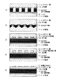
本実施の形態のDFBレーザの回折格子は複素屈折率の実部と虚部の摂動よりなり、屈折率結合と利得結合を同時に有する複素結合型とし、位相シフト領域を有する。複素結合型の回折格子を形成するには、図1に示す共振器軸方向断面の模式図のように、例えば、“1.55μm index/gain coupled DFB lasers with strained layer multiquantum−well active grating, ”G.P.Li et al,(Electron Lett.,vol.28,no.18,pp. 1726−1727, Aug. 1992.)に示されている▲1▼活性層(例えば図示のGaInAsP SCH−歪MQW層12における活性層12a)の一部もしくは全部をエッチングする方法や、例えば、“Fabrication and characteristics of gain−coupled distributed feedback semiconductor lasers with a corrugated active layer, ”Y. Luo et al,(IEEE J. Quantum Electron, vol. QE−27, no. 6, pp. 1724−1731,June 1991.)に示されている▲2▼パターン基板(例えば図示のn−InP基板11)上に活性層(例えば図示のGaInAsP MQW23における活性層23a)を形成する方法や、例えば、“1.55μm Gain−Coupled Quantum−Well Distributed Feedback Lasers with High Single−Mode Yield and Narrow Linewidth, ”B.Borchert et al,(IEEE Trans. Photon. Technol., Lett., vol. 3, no. 11, pp. 955−957, Nov. 1991.) に示されている▲3▼活性層(例えば図示のGaInAsP SCH−歪MQW層12における活性層12a)の上方もしくは下方に光吸収層(例えば図示のp−GaInAs光吸収層24)を周期的に設ける方法や、例えば、“Very−low threshold,highly efficient, and low−chirp 1.55μm complex−coupled DFB lasers with a current−blocking grating, ”Z. M. Chuang et al,(IEEE Photon. Technol. Lett., vol. 8, no. 11, pp. 1438−1440, Nov. 1996.) に示されている▲4▼活性層(例えば図示のGaInAsP SCH−歪MQW層12における活性層12a)の上方もしくは下方に電流阻止層(例えば図示のn−InGaAsP電流阻止層25)を周期的に設ける方法や、例えば、“Cain−coupled DFB lasers with a titanium surface Bragg grating.”T.W.Johannes et al,(Electron. Lett., vol. 31, no. 5, pp. 370−371, Mar. 1995.) に示されている▲5▼素子表面に金属による回折格子(例えば図示の金属回折格子27)を設ける方法などがある。
【0025】
位相シフト領域より前方、つまりレーザ光を取り出す端面方向の第1の回折格子の長さをL1、その複素結合係数を屈折率結合係数をki1、利得結合係数をkg1としてk1=ki1+ikg1とし、後方の第2の回折格子の長さをL2とし、後方の第1の回折格子のブラック波長に対しての複素結合係数を屈折率結合係数をki2、利得結合係数をkg2としてk2=ki2+ikg2としたとき、
ki1≠0,kg1≠0,ki2≠0,kg2≠0
|k1|×L1>|k2|×L2>0
とする。さらに、上述の構造において、|k1|およびL1と|k2|およびL2の大きさを位相シフトにより生じた共振モードの閾値利得αth_shよりもストップバンドの外側かつストップバンドに最近接の共振モードの閾値利得αth_exを小さくするように、すなわち、
αth_sh>αth_ex
となるように|k1|およびL1と|k2|およびL2の大きさを調節する。閾値利得は、例えば、“Coupled−Wave Theory of Distributed Feedback Lasers”H. Kogelnik et al,(J. Appl. Phys., vol. 43, no. 5, pp. 2327−2335, May 1972) や“A new exact and efficient numerical matrix theory of complicated laser structures: Properties of asymmetric phase−shifted DFB lasers,”G. Bjork et al,(J. Lightwave Technol., vol. LT−5, pp. 140−146, Jpn. 1987) などに記載の、結合波方程式や伝播行列法などにより求めることが可能である。また、結合係数を調節する方法としては、▲1▼回折格子の山と谷の比を変える、▲2▼回折格子の山の高さを変える、▲3▼導波路幅を変えて等価屈折率を変える、▲4▼導波路厚(上下の層の厚さ)を変えて等価屈折率を変えるなどが挙げられる。
【0026】
このとき、最も小さい閾値利得を持つモードは、屈折率と利得の摂動が同相である場合には、ストップバンドの長波長側のモードであり、屈折率と利得の摂動が逆相である場合には、ストップバンドの短波長側のモードである。
【0027】
<作用>
後端面への高反射率膜のコーティングは、その回折格子に対する位相により出来上がるレーザの特性が変化する。しかしながら、例えば、“High Single−mode Yield 1.55 μm GaInAsP/InP BH−DFB Lasers with Periodic Wirelike Active Regions,”N. Nunoya et al, (The 17th IEEE International Semiconductor Laser Conference, pp. 45−46, Sep. 2000)で述べられている活性層をエッチングすることによって作製した利得変化と屈折率変化が同相である回折格子を備えた複素結合型均一回折格子DFBレーザにおいては、均一回折格子であっても非対称端面反射率コーティングによらずストップバンドの長波長側の共振モードで発振し、単一波長動作の指標である発振モードと次モードの出力比である副モード抑圧比(SMSR)が30dB以上の単一波長動作が得られる。また、へき開による反射率30%程度以下の端面反射率であれば、その回折格子に対する位相によらず、発振波長は常にストップバンドの長波長側の波長となる。
【0028】
次に、非対称化を行うため、複素結合型DFBレーザの回折格子への位相シフトの導入を考える。位相シフトにより共振可能となるストップバンドの中に生じるモード、例えば、λ/4位相シフトの場合においてはブラッグ波長が発振波長となると、位相シフト部への光の集中が極端に増加しホールバーニングが生じるため、それに伴う局所的な屈折率の変化によりやはり特性の劣化を招く。このことを逆に考えると、位相シフトを導入しても、それにより存在可能となったストップバンド内の共振モードが発振モードとはならず、他の波長が発振するのであれば、共振器内部の光強度分布も滑らかとなり、空間的軸方向ホールバーニングを抑制できる。位相シフトにより生じたストップバンド内の共振モードでの発振を抑制するためには、位相シフト領域の前方、もしくは、後方の複素結合係数(k1=ki1+ikg1,k2=ki2+ikg2)と共振器長との積、すなわち、|k1|・L1もしくは|k2|・L2を小さくする。このとき、位相シフトによるモードは、発振に必要な光の帰還が十分得られず閾値利得が上昇し、ki1とkg1、もしくは、ki2とkg2、が同符号のときは、ストップバンドの長波長側の波長が最低閾値利得を有する波長となって発振が起こり、ki1とki2、もしくは、ki2とkg2、が異符号のときは、ストップバンドの短波長側の波長が最低閾値利得を有する波長となって発振が起こる。これは、あたかも|k1|・L1もしくは|k2|・L2のうち大きな値を有する回折格子による均一回折格子DFBレーザのようであり、共振器内部の光分布も均一回折格子DFBレーザのそれと似た傾向となるため、位相シフト領域への光の集中は起きず、ホールバーニングは抑制される。
【0029】
以上のことを図2に示す本発明の原理の図を用いて説明する。座標Zは共振器軸方向に沿って共振器前端面を0とした。簡単化のために両端面はARコーティング膜17を施して無反射とし、第1の回折格子18と第2の回折格子19の周期および結合係数は同じである場合を考える。まず、回折格子が屈折率結合型の場合を考える。図3に屈折率結合型DFBレーザの場合のスペクトルの計算例を示す。20の位相シフト位置がL1/(L1+L2)=0.5の位置にあるとき、λ/4位相シフトによるモードがストップバンドの中央にできるが、L1/(L1+L2)=0.8とすることで、k2・L2が小さくなり、ブラッグ波長の閾値利得が上昇し、ストップバンドの両側のモードの閾値利得が最小となるため、ブラッグ波長では発振しない。ただし、屈折率結合の場合、ストップバンドの両側のモードの閾値利得がほぼ同等となるので、スペクトルの計算結果からも明らかなように単一モード動作が得られない。次に、回折格子が屈折率と利得の摂動が同相である複素結合型の場合を考える。図4に、複素結合型DFBレーザの場合のスペクトル計算結果を示す。位相シフト20がL1/(L1+L2)=0.5の位置にあるとき、λ/4位相シフトによるモードがストップバンドの中央にできるのは、前述の屈折率結合型DFBレーザの場合と同様である。しかしながら、L1/(L1+L2)=0.8とすることで、k2・L2が小さくなると、均一回折格子の場合と同じようにストップバンドの長波長側のモードの閾値利得が最小となり単一モード動作する。すなわち、本発明の動作原理は複素結合型回折格子によるDFBレーザに特徴的な現象を用いたものである。
【0030】
図5に示した複素結合型DFBレーザにおける位相シフト位置を変えた場合の共振器内部の光パワー密度分布の計算例を見ると、同じ前方出力を得ようとした場合、λ/4位相シフトを中央部に入れたL1/(L1+L2)=0.5や前方出力を大きくするためにλ/4位相シフト部を前方に置いたL1/(L1+L2)=0.4の場合、λ/4位相シフトにより生じるストップバンド内のモード、すなわちブラック波長が共振モードとなるため、位相シフト部への光の集中が大きくなる。これは、屈折率結合型DFBレーザの場合も同様である。一方で、L1/(L1+L2)=0.8の場合は、図4で示したようにストップバンドの外側の波長で発振するため、位相シフト部への極端な光の集中は起きず起伏の緩やかな平坦に近い分布となる。このとき、位相シフトを前方よりに挿入した場合の前後端面の出力比とほぼ同じ出力比が得られる。また、図5からわかるように、前方端面からの出力を後方端面からの出力よりも大きくする場合には、位相シフト位置を後方に置く、すなわち、|k2|・L2を|k1|・L1よりも小さくする。
【0031】
前述のように、複素結合型回折格子の場合、均一回折格子の場合でも単一波長動作が可能であり、端面反射の影響を受けにくいため、端面の無反射(AR)コーティング膜は、必ずしも完全である必要は無く、へき開面程度以下の反射率であれば良い。加えて位相シフトが存在するため、共振器構造は非対称となり、複素結合係数と共振器長との積を小さくした側とは反対の端面から光が出射する割合が増大する。位相シフトは、共振構造を非対称化するためのものであり、位相シフトによる共振モードは発振させないため、位相シフト量は必ずしもλ/4である必要は無い。
【0032】
次に、回折格子の構造について述べる。第2の回折格子19の結合係数と回折格子長さの積を小さくする、特に、結合係数を小さくする場合を考える。第1の方法は、第1の回折格子18よりも第2の回折格子19側の回折格子の山の高さを低くすることによって結合係数を小さくすることができる。ただし、2つの領域を別々に作製しなければ精度良く作製することは難しいと考えられる。第2の方法は、回折格子の山谷の比を1:1からずらすことで結合係数を小さくすることが可能である。この方法によれば、同時に異なる結合係数を有する2つの回折格子を作製可能である。しかしながら、例えば1.55μm波長帯の1次の回折格子の場合、回折格子周期は240nmであり、この中で山谷の比を精度良く制御することは困難である。第3の別の方法としては、優れたレーザ特性を得るためには1次の回折格子が望ましいが、高次の回折格子によっても動作原理は変わらないため、結合係数と回折格子長さの積を小さくするために高次回折格子を用いても良い。この方法によれば、例えば、1次の回折格子と2次の回折格子を同時に形成することが可能であり加工制御性も改善される。さらに別の第4の方法を考えると、回折格子の山をm個中n個の割合で残す方法(m>n)等により、平均的な結合係数をn/mと減少させることによって回折格子のk・Lを調節してもよい。
【0033】
ここで、図6〜図8に基づき、本発明の実施例について説明する。
【0034】
<第1実施例>
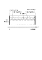
図6は、本発明の第1実施例[請求項1、請求項2に対応]であり、複素結合型分布帰還型半導体レーザの構造を示す断面図である。図6において、11はInP基板、12は発光波長1.55μmのInGaAsPの多層歪量子井戸(MQW)活性層とそれを挟み込むバンドギャップ波長1.2μmのSCH層よりなるSCH−歪MQW層、13はp−InPクラッド層、14はp−コンタクト層、15はp側電極、16はn側電極、17はARコーティング膜、18,19は第1,第2の回折格子である。
【0035】
第1の回折格子18および第2の回折格子19は、SCH−歪MQW層12を周期(Λ)240nmでエッチングしInPにより埋め込み再成長することにより形成されるため、屈折率と利得の摂動により回折格子が構成され、それぞれ同じ大きさの複素結合係数k1とk2を有する。屈折率結合係数はおよそ360cm−1であり、利得結合係数を正確に見積もることは困難であるが、およそ数〜数十cm−1となる。回折格子の作製法は、本実施例では図1に示されている▲1▼MQW層(活性層)のエッチングによるもの[請求項5に対応]であるが、同図の他の方法、即ち、▲2▼パターン基板上に活性層を形成する方法[請求項6に対応]や、活性層の上方もしくは下方に光吸収層を周期的に設ける方法[請求項7に対応]や、▲4▼活性層の上方もしくは下方に電流阻止層を周期的に設ける方法[請求項8に対応]や、▲5▼表面金属回折格子による方法[請求項9に対応]などによって複素結合型回折格子を実現しても良い。λ/4位相シフト領域20を挟んで、前方の第1の回折格子18の長さをL1=160μmとし、後方の第2の回折格子19の長さをL2=40μmとしており、λ/4位相シフト領域が、
|k1|×L1>|k2|×L2>0
を満たすように形成されている。
【0036】
活性層は、バルクでもかまわないが、歪MQW層とすることにより光出力特性が向上するため、ここでは歪MQW層を用いている。レーザ構造は、導波路の両脇を極性の異なる半導体層を積層した電流阻止層や半絶縁体層で埋め込んだ埋め込みヘテロ構造としている。しかし、本発明の原理はリッジ構造やその他の導波路構造でもなんら問題はない。
【0037】
本第1実施例の構造により、最低閾値利得を有するモードは、λ/4位相シフトによるブラック波長とはならず、ストップバンドの長波長側のモードとなるため、ホールバーニング効果が抑制される。また、単一波長動作であり、35dB以上の副モード抑圧比(SMSR)が得られる。さらに、非対称構造となるため、第1の回折格子18側からの出力、すなわち出射端面側からの出力が第2の回折格子19側、すなわち後端面側からの出力よりも大きくなり、8以上の出力比が得られる。本実施例はInP基板11上のGaInAsP量子井戸を用いた例であるが、例えばGaAsなどのInP以外の材料の基板を用いても原理的に本発明を適用可能なのは明らかである。
【0038】
<第2実施例>
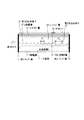
図7は、本発明の第2実施例[請求項1、請求項3に対応]であり、本第2実施例では図6に示した第1実施例の構造図中の第2の回折格子19の次数を第1の回折格子18の次数より高次にする。
【0039】
具体的には、本第2実施例では、第1の回折格子18の周期(Λ1)を1.5μm波長帯の1次の回折格子周期である240nmとし、第2の回折格子19の周期(Λ2)を2次の回折格子周期である480nmとした。λ/4位相シフト領域20を挟んで、第1の回折格子18の長さをL1=120μmとし、第2の回折格子19の長さをL2=80μmとしており、λ/4位相シフト領域20が、
|k1|×L1>|k2|×L2>0
を満たすように形成されている。これにより、第1実施例と同じ効果が得られる。
【0040】
<第3実施例>
図8は、本発明の第3実施例[請求項1、請求項4に対応]であり、本第3実施例では図6に示した第1実施例の構造図中の第2の回折格子19の山をm個中、n個にして平均的な結合係数を下げる。
【0041】
具体的には、本第3実施例では、第1の回折格子18と第2の回折格子19の周期が同じ240nmであるが、第2の回折格子19の山3つのうち1つを除去した。λ/4位相シフト領域20を挟んで、第1の回折格子18の長さをL1=140μmとし、第2の回折格子19の長さをL2=60μmとしており、λ/4位相シフト領域20が、
|k1|×L1>|k2|×L2>0
を満たすように形成されている。これにより、第1実施例と同じ効果が得られる。
【0042】
【発明の効果】
以上説明したように、本発明の複素結合型分布帰還型半導体レーザによれば、副モード抑圧比の大きな劣化無しで、非対称端面コーティング膜を用いずに、両端面共に無反射コーティングとしても出力を非対称化することが可能であるため、高反射端面コーティングの回折格子に対する位置の不確定性による発振波長の不安定性を除去できる。さらには、端面コーティングが困難な集積光回路構成に用いる良好な光源が実現できる。また、必ずしも端面無反射コーティングが必要では無く、端面コーティングプロセスを削除できるため、コスト低下においても有効である。さらに、位相シフトにより生じる共振モードを用いないため、スペクトルホールバーニングを抑制でき、高出力時にも安定した特性が得られる。
【図面の簡単な説明】
【図1】複素結合型回折格子を説明する図である。
【図2】発明原理を説明する図である。
【図3】発振波長を説明する図(屈折率結合型DFBレーザの場合)である。
【図4】発振波長を説明する図(複素結合型DFBレーザの場合)である。
【図5】共振器内部の光のパワー密度分布の計算例である。
【図6】本発明の第1実施例の複素結合型分布帰還型半導体レーザを説明する図である。
【図7】本発明の第2実施例の複素結合型分布帰還型半導体レーザを説明する図である。
【図8】本発明の第3実施例の複素結合型分布帰還型半導体レーザを説明する図である。
【図9】従来技術を説明する図である。
【符号の説明】
11 n−InP基板
12 GaInAsP SCH−歪MQW層
13 p−InPクラッド層
14 p−GaInAsコンタクト層
15 p側電極
16 n側電極
17 ARコーティング膜
18 回折格子1
19 回折格子2
20 位相シフト
21 GaInAsPガイド層
22 HRコーティング膜
23 GaInAsP MQW
24 p−GaInAs光吸収層
25 n−InGaAsP電流阻止層
26 i−InP
27 金属回折格子[0001]
TECHNICAL FIELD OF THE INVENTION
The present invention relates to a distributed feedback semiconductor laser, and more particularly to a complex-coupled distributed feedback semiconductor laser having a diffraction grating constituted by perturbations of both the refractive index and the gain.
[0002]
[Prior art]
A distributed feedback semiconductor laser (hereinafter, referred to as a DFB laser) can oscillate at a single wavelength even during modulation by utilizing black reflection by a diffraction grating formed in an active region. It is used as a light source. DFB lasers can be classified into several types according to their diffraction gratings. In general, a DFB laser having a diffraction grating consisting of a real part of a complex refractive index, that is, a refractive index perturbation is used as an index-coupled type. A) a DFB laser having a diffraction grating consisting of a imaginary part of a complex refractive index, that is, a perturbation of gain or loss; a gain-coupled DFB laser, a perturbation of both a real part and an imaginary part of a complex refractive index; A DFB laser having a diffraction grating is referred to as a complex-coupled DFB laser. Further, the DFB laser provided with a diffraction grating having a uniform period and a coupling coefficient over the entire resonator can be classified based on the period and phase of the diffraction grating, or the like. The DFB laser whose phase is shifted by a minute is referred to as a λ / 4 shift DFB laser.
[0003]
In a laser, the gain of an optical waveguide at which laser oscillation determined by a resonator structure starts is called a threshold gain. In a DFB laser, different modes oscillating at different wavelengths have different threshold gains, and the lowest threshold gain is obtained. It oscillates in the mode that it has. Generally, in an optical waveguide having a diffraction grating, a wavelength band in which transmission of light is significantly hindered, that is, a wavelength band having a high reflectance is called a stop band (stop band). In a refractive index-coupled uniform diffraction grating DFB laser, a stop band is used. The same threshold gain is obtained in the mode on the long wavelength side closest to the stopband and the mode on the short wavelength side closest to the stop band. Difference in threshold gain between the mode with the lowest threshold gain and the mode with the next lowest threshold gain, even if single-wavelength operation is obtained due to asymmetry of the surrounding environment such as temperature and temperature, or asymmetry due to manufacturing errors. Is small, the mode is easily changed by a modulation operation or the like, so that stable single-wavelength operation cannot be obtained. Therefore, in order to obtain the single-wavelength oscillation operation of the refractive index-coupled uniform diffraction grating, generally, as shown in FIG. Coating films having different reflectances (for example, an anti-reflection (AR) coating film 17 and a high-reflection (HR) coating film 22) are applied. Further, according to the asymmetrical reflectance coating film, the laser output emitted from both end faces is also asymmetrical, and a large output is obtained from the low reflectance end face side. However, for example, as described in
[0004]
On the other hand, in a refractive index coupling type λ / 4 shift DFB laser, there is usually a phase shift region in the central portion in the resonator axis direction, and both end surfaces of the resonator are coated with an anti-reflection coating to reduce the equivalent refractive index of the waveguide. neq , The period of the diffraction grating is Λ, and the order of the diffraction grating is q, the λ / 4 shift
λB= 2neqΛ / q
In the black wavelength occurring in the stop band, the threshold gain is the smallest at the black wavelength, the single wavelength operation is performed, and the threshold gain difference from the mode having the next lower threshold gain is also the refraction with the asymmetric reflectance coating film. The single-wavelength operation characteristic is excellent because it can be larger than the rate-coupling type uniform diffraction grating DFB laser. However, in a refractive index coupling type λ / 4 shift DFB laser having a λ / 4 shift section at the center of the resonator, the light output from both end faces is equivalent, and the refractive index generally provided with the asymmetrical reflectance coating film described above. The light output that can be extracted from the front is smaller than that of the coupling-type uniform diffraction grating DFB laser.
[0005]
In order to improve the disadvantages of the above-described index-coupled λ / 4 shift DFB laser, for example, in Non-Patent
[0006]
Further, when the λ / 4 phase shift is provided, and the phase condition is satisfied at the black wavelength and the oscillation wavelength is reached, the reflectance of the diffraction grating having a large kL becomes high. Of these, the ratio of output to the side of the diffraction grating with a small kL increases. For example, in Non-Patent Document 3, in a λ / 4 phase shift DFB laser in which antireflection coating is applied to both end surfaces, as shown in FIG. 9B, the λ / 4 phase shift point 20 is set at the center of the resonator axis direction. , The kL of the first diffraction grating 18 before the phase shift point 20 is made smaller than the kL of the second diffraction grating 19 after the phase shift point 20, thereby increasing the single wavelength characteristic. A method for improving the forward light output without deterioration is described. Also in this example, the oscillation wavelength is the black wavelength. However, as the output asymmetry increases, the threshold gain of the oscillation wavelength increases, the threshold current, which is the current value at which oscillation starts, increases, and the threshold gain difference with the wavelength having the next lower threshold gain decreases. As a result, the single-wavelength characteristic deteriorates, so that the asymmetry cannot be increased beyond a certain level.
[0007]
In the above-described example, kL is made asymmetric by changing L of the first and
[0008]
By the way, the carrier concentration distribution of the active layer is generated by the field distribution of light in the resonator axis direction generated inside the resonator, and the equivalent refractive index of the waveguide changes accordingly, that is, the spatial axial hole burning phenomenon. This also causes the threshold gain difference between the oscillation wavelength having the lowest threshold gain and the wavelength having the next lowest threshold gain to decrease, deteriorating the single-wavelength operation characteristic. However, in a λ / 4 phase shift DFB laser, This is a major problem when oscillating at the Bragg wavelength. In spatial axial hole burning, the reflectance increases as the value of kL increases, and the concentration of light on the phase shift unit becomes significant. This poses a serious problem, and lower threshold current operation and shorter resonators of the laser are limited. You. Therefore, the structures illustrated in FIGS. 9B and 9C using the oscillation at the black wavelength, and the spatial axial hole burning becomes a problem. When the phase shift amount is λ / 4, the phase condition is perfectly matched at the Bragg wavelength, but even if the phase shift amount deviates from λ / 4, resonance is possible at a wavelength deviated from the Bragg wavelength by the deviated phase amount. In the case of oscillation in a mode in which resonance is possible due to phase shift, a problem of spatial axial hole burning occurs.
[0009]
On the other hand, for example, as described in Non-Patent Document 4, a complex-coupled DFB laser can operate at a single wavelength even with a uniform diffraction grating. When the perturbation of the refractive index and the perturbation of the gain are in phase, that is, when the high refractive index portion and the high gain portion, and the low refractive index portion and the low gain portion match, This is the resonance mode closest to the stop band on the long wavelength side of the stop band, and when the perturbation of the refractive index and the perturbation of the gain are in antiphase, that is, the high refractive index part, the low gain part, and the low refractive index part When the high gain and the high gain part match, the resonance mode is the resonance mode closest to the stop band on the short wavelength side of the stop band. However, the light emitted from both end faces of the resonator is basically equal because of the uniform diffraction grating. Therefore, for example, a coating film having a different reflectance must be applied to each end face, and thus, as in the case of the refractive index-coupled DFB laser, the uncertainty of the oscillation wavelength and the yield of single-wavelength operation are reduced. Deterioration occurs. In addition, when the λ / 4 phase shift region is introduced into the diffraction grating, the problem of the hole burning phenomenon occurs when the Bragg wavelength becomes the oscillation wavelength.
[0010]
[Non-patent document 1]
"Effect of Mirror Factors on Leasing Characteristics of Distributed Feedback InGaAsP / InP Laser Diodes at 1.5 [mu] m Range," Utaka et al (IEEE J. Quantum Electron., QE-20, No. 3, pp. 236-245, March 1984).
[Non-patent document 2]
"Analysis of [lambda] / 4-phase shifted DFB LD" M. Yamaguchi et al. (In 1985 Nat. Conv. Rec., IECE Japan, p. 310).
[Non-Patent Document 3]
"Asymmetric Metric / 4-Shift InGaAsP / InP DFB Lasers" Usami et al, (IEEE J. Quantum Electron., QE-23, p. 815-821, July 1987).
[Non-patent document 4]
“High Single-mode Yield 1.55 μm GaInAsP / InP BH-DFB Lasers with Periodic Wirelike Active Regions,” N. Nunya et al, (The 17th IEEE International Semiconductor Laser Conference, pp. 45-46, September 2000)
[Patent Document 1]
JP-A-11-163364
[0011]
[Problems to be solved by the invention]
As described above, the conventional index-coupled DFB laser and the complex-coupled DFB laser have the following problems when operating at a single wavelength and asymmetrical front and rear outputs. In the case of a method using an asymmetric coating film in a uniform diffraction grating DFB laser, that is, when a low reflectance coating film is applied to the front end face and a high reflectance coating film is applied to the rear end face, a single wavelength characteristic is obtained by the phase with respect to the diffraction grating at the end face. There is a problem of deterioration and an unstable oscillation wavelength. Also, in the method of setting the λ / 4 phase shift position on the high reflectivity end face behind the center in the resonator axial direction after forming the asymmetric coating film, the reflection end face is also set similarly to the case of the uniform diffraction grating. There is a problem in that the phase with respect to the diffraction grating degrades the single wavelength characteristic and the oscillation wavelength becomes uncertain.
[0012]
On the other hand, in a method in which both end faces are made low-reflection and the position of the phase shift region is positioned ahead of the center of the resonator, the threshold current increases and the single-wavelength characteristics deteriorate as the asymmetry increases. Further, when a phase shift is introduced and oscillation occurs in a resonance mode generated in a stop band due to the phase shift, axial hole burning becomes a problem.
[0013]
The present invention has been made to solve such a problem. In a DFB laser, a high single-wavelength oscillation characteristic is maintained irrespective of asymmetrical end face coating, and light emitted from an end face of a resonator is forward and backward. It is an object of the present invention to asymmetrically suppress the hole burning due to the introduction of the phase shift.
[0014]
[Means for Solving the Problems]
A complex-coupled distributed feedback semiconductor laser according to a first aspect of the present invention (claim 1) that solves the above problem has a real part, that is, a refractive index and an imaginary part, of a complex refractive index sandwiching a phase shift point or a region, that is, both gain and loss. In a distributed feedback laser diode having two diffraction gratings formed by perturbation, the direction in which the main laser light is emitted is set to the front, and the length of the first diffraction grating before the phase shift point or region is set to L.1, The length of the second diffraction grating behind the phase shift point or region is L2, The complex coupling coefficient of the first diffraction grating ahead of the phase shift point or area is represented by the refractive index coupling coefficient k.i1, And the gain coupling coefficient is kg1As k1= Ki1+ Ikg1And the complex coupling coefficient of the second diffraction grating behind the phase shift point or the area is defined as the refractive index coupling coefficient k.i2, And the gain coupling coefficient is kg2As k2= Ki2+ Ikg2When we define
ki1≠ 0, kg1≠ 0, ki2≠ 0, kg2$ 0
| K1| × L1> | K2| × L2> 0
And the threshold gain of the mode generated in the stop band due to the phase shift is αth_sh, The threshold gain of the mode outside the stop band and closest to the stop band is αth_exAnd when
αth_sh> Αth_ex
| K1| And L1And | k2| And L2The size is adjusted.
[0015]
The complex-coupled distributed feedback semiconductor laser according to the second invention (claim 2) is the complex-coupled distributed feedback laser according to the first invention, and has a length L1Complex coupling coefficient k of the first diffraction grating1And the length L2Complex coupling coefficient k of the second diffraction grating2Are the same,
L1> L2
And the threshold gain of the mode generated in the stop band due to the phase shift is αth_sh, The threshold gain of the mode outside the stop band and closest to the stop band is αth_exAnd when
αth_sh> Αth_ex
To satisfy1And L2The size is adjusted.
[0016]
Further, a complex-coupled distributed feedback semiconductor laser according to a third invention (claim 3) is the complex-coupled distributed feedback laser according to the first invention, wherein the order of the first diffraction grating is p, When the order of the diffraction grating is q,
| K1| × L1> | K2| × L2> 0
To satisfy the relationship
p <q
And the threshold gain of the mode generated in the stop band due to the phase shift is αth_sh, The threshold gain of the mode outside the stop band and closest to the stop band is αth_exAnd when
αth_sh> Αth_ex
| K1| And L1And | k2| And L2The size is adjusted.
[0017]
Further, the complex-coupled distributed feedback semiconductor laser according to the fourth invention (claim 4) is the complex-coupled distributed feedback laser according to the first invention or the third invention, wherein the first diffraction grating or the second diffraction grating is used. Either or both of the gratings leave the peaks of the grating in n out of m (m> n), thereby reducing the average coupling coefficient to n / m. And the average coupling coefficient satisfies the condition of
αth_sh> Αth_ex
| K1| And L1And | k2| And L2The size is adjusted.
[0018]
The complex-coupled distributed feedback semiconductor laser according to the fifth invention (claim 5) is the complex-coupled distributed feedback semiconductor laser according to any one of the first to fourth inventions, wherein the complex-coupled diffraction grating is Is manufactured by etching a part or the whole of the multiple quantum well active layer.
[0019]
The complex-coupled distributed feedback semiconductor laser according to the sixth invention is the complex-coupled distributed feedback semiconductor laser according to any one of the first to fourth inventions, wherein the complex-coupled diffraction grating is provided on the pattern substrate. It is characterized by being produced by growing an active layer.
[0020]
The complex-coupled distributed feedback semiconductor laser according to the seventh invention is the complex-coupled distributed feedback semiconductor laser according to any one of the first to fourth inventions, wherein the complex-coupled diffraction grating is located above the active layer. Alternatively, it is characterized by being manufactured by periodically providing a light absorbing layer below.
[0021]
The complex-coupled distributed feedback semiconductor laser according to the eighth invention is the complex-coupled distributed feedback semiconductor laser according to any one of the first to fourth inventions, wherein the complex-coupled diffraction grating is located above the active layer. Alternatively, it is characterized by being produced by periodically providing a current blocking layer below.
[0022]
The complex-coupled distributed feedback semiconductor laser according to the ninth aspect is the complex-coupled distributed feedback semiconductor laser according to any one of the first to fourth aspects, wherein the complex-coupled diffraction grating has a metal surface on the element surface. It is characterized by being produced by providing a film periodically.
[0023]
BEST MODE FOR CARRYING OUT THE INVENTION
Hereinafter, embodiments of the present invention will be described in detail with reference to the drawings. The DFB laser structure according to the embodiment of the present invention solves the problem by the following diffraction grating structure.
[0024]
The diffraction grating of the DFB laser according to the present embodiment is a complex coupling type having a perturbation of a real part and an imaginary part of a complex refractive index, has a refractive index coupling and a gain coupling at the same time, and has a phase shift region. To form a complex-coupling type diffraction grating, for example, as shown in a schematic diagram of a cross section in the resonator axial direction shown in FIG. 1, for example, “1.55 μm index / gain coupled DFB lasers with strained layer multiquantum-well active,” G. FIG. P. Li et al, (Electron Lett., Vol. 28, no. 18, pp. 1727-1727, Aug. 1992.) (1) Active layer (for example, in the illustrated GaInAsP SCH-strained MQW layer 12). A method of etching a part or the whole of the active layer 12a), for example, “Fabrication and characteristics of gain-coupled distributed feedback semiconductor lasers with a certifier. Luo et al, (IEEE J. Quantum Electron, vol. QE-27, no. 6, pp. 1727-1731, June 1991.) (2) Pattern substrate (for example, n-
[0025]
The length of the first diffraction grating in front of the phase shift region, that is, in the direction of the end face from which the laser light is extracted, is L1, And its complex coupling coefficient is ki1, And the gain coupling coefficient is kg1As k1= Ki1+ Ikg1And the length of the rear second diffraction grating is L2And the complex coupling coefficient for the black wavelength of the rear first diffraction grating is ki2, And the gain coupling coefficient is kg2As k2= Ki2+ Ikg2And when
ki1≠ 0, kg1≠ 0, ki2≠ 0, kg2$ 0
| K1| × L1> | K2| × L2> 0
And Further, in the above structure, | k1| And L1And | k2| And L2Threshold gain α of the resonance mode caused by the phase shiftth_shThreshold gain α of the resonance mode outside the stop band and closest to the stop bandth_ex, Ie,
αth_sh> Αth_ex
| K1| And L1And | k2| And L2Adjust the size of. The threshold gain is described in, for example, “Coupled-Wave Theory of Distributed Feedback Lasers” H. Kogelnik et al., (J. Appl. Phys., Vol. 43, no. DFB lasers, "G. Bjork et al., (J. Lightwave Technology, vol. LT-5, pp. 140-146, Jpn. 1987), etc., can be used for the calculation. Methods for adjusting the coupling coefficient include: (1) changing the ratio of the peaks and valleys of the diffraction grating; (2) changing the height of the peaks of the diffraction grating; and (3) changing the waveguide width. And (4) changing the equivalent refractive index by changing the waveguide thickness (thickness of upper and lower layers).
[0026]
At this time, the mode having the smallest threshold gain is a mode on the longer wavelength side of the stop band when the refractive index and the gain perturbation are in phase, and when the refractive index and the gain perturbation are out of phase. Is a mode on the short wavelength side of the stop band.
[0027]
<Action>
When the rear end face is coated with a high-reflectance film, the characteristics of the laser formed vary depending on the phase with respect to the diffraction grating. However, see, for example, "High Single-mode Yield 1.55 [mu] m GaInAsP / InP BH-DFB Lasers with Periodic Wireless Active Regions," Nunya et al, (The 17th IEEE International Semiconductor Laser Conference, pp. 45-46, Sep. 2000), a complex-coupled uniform diffraction grating DFB laser having a diffraction grating in which the gain change and the refractive index change have the same phase produced by etching the active layer is asymmetric even if the uniform diffraction grating is used. It oscillates in the resonance mode on the long wavelength side of the stop band irrespective of the end face reflectance coating, and has a single mode suppression ratio (SMSR) of 30 dB or more, which is an output ratio between the oscillation mode and the next mode, which is an index of single wavelength operation. One wavelength operation is obtained. If the end face reflectivity is about 30% or less due to cleavage, the oscillation wavelength is always the long wavelength side of the stop band regardless of the phase with respect to the diffraction grating.
[0028]
Next, in order to perform asymmetry, introduction of a phase shift into the diffraction grating of the complex-coupled DFB laser will be considered. When a Bragg wavelength becomes an oscillation wavelength in a mode generated in a stop band capable of resonating due to a phase shift, for example, in the case of a λ / 4 phase shift, the concentration of light on the phase shift portion increases extremely and hole burning occurs. As a result, the local change in the refractive index also causes deterioration of the characteristics. Considering this conversely, even if a phase shift is introduced, the resonance mode in the stop band that can be present due to the phase shift does not become an oscillation mode, and if another wavelength oscillates, the inside of the resonator Has a smooth light intensity distribution, and can suppress spatial axial hole burning. In order to suppress the oscillation in the resonance mode in the stop band caused by the phase shift, the complex coupling coefficient (k1= Ki1+ Ikg1, K2= Ki2+ Ikg2) And the length of the resonator, that is, | k1| ・ L1Or | k2| ・ L2Smaller. At this time, in the mode based on the phase shift, sufficient feedback of light required for oscillation cannot be obtained, the threshold gain increases, and ki1And kg1Or ki2And kg2, Have the same sign, the wavelength on the long wavelength side of the stop band becomes the wavelength having the minimum threshold gain, and oscillation occurs, and ki1And ki2Or ki2And kg2, Have different signs, the wavelength on the short wavelength side of the stop band becomes the wavelength having the minimum threshold gain, and oscillation occurs. This is as if | k1| ・ L1Or | k2| ・ L2It is like a uniform diffraction grating DFB laser with a diffraction grating having a large value, and the light distribution inside the resonator also has a similar tendency to that of the uniform diffraction grating DFB laser, so that light concentration in the phase shift region occurs. And hole burning is suppressed.
[0029]
The above will be described with reference to the diagram of the principle of the present invention shown in FIG. The coordinate Z is set to 0 at the front end face of the resonator along the resonator axis direction. For the sake of simplicity, it is assumed that the both end faces are provided with an AR coating film 17 so as to be non-reflective, and the periods and the coupling coefficients of the first diffraction grating 18 and the
[0030]
In the calculation example of the optical power density distribution inside the resonator when the phase shift position is changed in the complex-coupled DFB laser shown in FIG. 5, when trying to obtain the same forward output, the λ / 4 phase shift is changed. L in the center1/ (L1+ L2) = 0.5 or L in which a λ / 4 phase shift unit is placed in front to increase the front output.1/ (L1+ L2) = 0.4, the mode in the stop band generated by the λ / 4 phase shift, that is, the black wavelength becomes the resonance mode, so that the concentration of light on the phase shift unit increases. This is the same in the case of the index-coupled DFB laser. On the other hand, L1/ (L1+ L2In the case of) = 0.8, oscillation occurs at a wavelength outside the stop band as shown in FIG. 4, so that an extreme concentration of light does not occur in the phase shift portion, and the distribution has a gently undulating and nearly flat distribution. . At this time, an output ratio substantially the same as the output ratio of the front and rear end faces when the phase shift is inserted from the front is obtained. Also, as can be seen from FIG. 5, when the output from the front end face is made larger than the output from the rear end face, the phase shift position is set backward, that is, | k2| ・ L2To | k1| ・ L1Smaller than
[0031]
As described above, in the case of a complex-coupling type diffraction grating, even a uniform diffraction grating can operate at a single wavelength and is hardly affected by end-face reflection. Therefore, the anti-reflection (AR) coating film on the end face is not necessarily perfect. It is not necessary that the reflectance be equal to or less than the cleavage plane. In addition, due to the presence of the phase shift, the resonator structure becomes asymmetric, and the rate of light emission from the end face opposite to the side on which the product of the complex coupling coefficient and the resonator length is reduced increases. The phase shift is for making the resonance structure asymmetric, and does not oscillate the resonance mode due to the phase shift. Therefore, the phase shift amount does not necessarily need to be λ / 4.
[0032]
Next, the structure of the diffraction grating will be described. Consider a case where the product of the coupling coefficient of the
[0033]
Here, an embodiment of the present invention will be described with reference to FIGS.
[0034]
<First embodiment>
FIG. 6 is a cross-sectional view showing a complex-coupled distributed feedback semiconductor laser according to a first embodiment of the present invention (corresponding to
[0035]
Since the first diffraction grating 18 and the
| K1| × L1> | K2| × L2> 0
It is formed so as to satisfy.
[0036]
The active layer may be bulk, but a strained MQW layer is used here because a light output characteristic is improved by using a strained MQW layer. The laser structure has a buried hetero structure in which both sides of the waveguide are buried with a current blocking layer in which semiconductor layers having different polarities are stacked or a semi-insulating layer. However, the principle of the present invention has no problem with a ridge structure or other waveguide structures.
[0037]
According to the structure of the first embodiment, the mode having the lowest threshold gain does not become the black wavelength due to the λ / 4 phase shift, but becomes the mode on the longer wavelength side of the stop band, so that the hole burning effect is suppressed. In addition, it is a single wavelength operation, and a sub-mode suppression ratio (SMSR) of 35 dB or more can be obtained. Further, because of the asymmetric structure, the output from the first diffraction grating 18 side, that is, the output from the output end face side becomes larger than the output from the
[0038]
<Second embodiment>
FIG. 7 shows a second embodiment of the present invention (corresponding to
[0039]
Specifically, in the second embodiment, the period of the first diffraction grating 18 (Λ1) Is 240 nm, which is the primary diffraction grating period in the 1.5 μm wavelength band, and the period of the second diffraction grating 19 (Λ2) Was set to 480 nm, which is the second-order diffraction grating period. With the λ / 4 phase shift region 20 interposed, the length of the first diffraction grating 18 is L1= 120 μm, and the length of the
| K1| × L1> | K2| × L2> 0
It is formed so as to satisfy. Thereby, the same effect as in the first embodiment can be obtained.
[0040]
<Third embodiment>
FIG. 8 shows a third embodiment of the present invention (corresponding to
[0041]
More specifically, in the third embodiment, the first diffraction grating 18 and the
| K1| × L1> | K2| × L2> 0
It is formed so as to satisfy. Thereby, the same effect as in the first embodiment can be obtained.
[0042]
【The invention's effect】
As described above, according to the complex-coupled distributed feedback semiconductor laser of the present invention, without significant deterioration of the submode suppression ratio, without using the asymmetrical end face coating film, the output can be obtained as a non-reflective coating on both end faces. Since the asymmetry can be achieved, the instability of the oscillation wavelength due to the uncertainty of the position of the highly reflective end face coating with respect to the diffraction grating can be eliminated. Furthermore, a good light source used for an integrated optical circuit configuration in which end face coating is difficult can be realized. Further, the end face anti-reflection coating is not necessarily required, and the end face coating process can be omitted, which is effective in reducing the cost. Furthermore, since a resonance mode caused by a phase shift is not used, spectral hole burning can be suppressed, and stable characteristics can be obtained even at high output.
[Brief description of the drawings]
FIG. 1 is a diagram illustrating a complex-coupled diffraction grating.
FIG. 2 is a diagram illustrating the principle of the invention.
FIG. 3 is a diagram for explaining an oscillation wavelength (in the case of a refractive index-coupled DFB laser).
FIG. 4 is a diagram for explaining an oscillation wavelength (in the case of a complex-coupling type DFB laser).
FIG. 5 is a calculation example of a power density distribution of light inside a resonator.
FIG. 6 is a diagram illustrating a complex-coupled distributed feedback semiconductor laser according to a first embodiment of the present invention.
FIG. 7 is a diagram illustrating a complex-coupled distributed feedback semiconductor laser according to a second embodiment of the present invention.
FIG. 8 is a diagram illustrating a complex-coupled distributed feedback semiconductor laser according to a third embodiment of the present invention.
FIG. 9 is a diagram illustrating a conventional technique.
[Explanation of symbols]
11 n-InP substrate
12 GaInAsP SCH-strained MQW layer
13 p-InP cladding layer
14 p-GaInAs contact layer
15 p-side electrode
16 n-side electrode
17 AR coating film
18
19
20 phase shift
21 GaInAsP guide layer
22 HR coating film
23 GaInAsP MQW
24 p-GaInAs light absorption layer
25 n-InGaAsP current blocking layer
26 i-InP
27 Metal grating
Claims (9)
ki1≠0,kg1≠0,ki2≠0,kg2≠0
|k1|×L1>|k2|×L2>0
であって、位相シフトによりストップバンド内に生じるモードの閾値利得をαth_sh、ストップバンドの外側かつストップバンドに最近接のモードの閾値利得をαth_exとしたとき、
αth_sh>αth_ex
を満たすように、|k1|およびL1と|k2|およびL2の大きさを調節したことを特徴とする複素結合型分布帰還型半導体レーザ。A main feedback laser beam is emitted from a distributed feedback laser diode having two diffraction gratings formed by perturbations of the real part of the complex refractive index, ie, the refractive index and the imaginary part, ie, both gain and loss, sandwiching the phase shift point or region. When the direction of the first diffraction grating is L 1 , and the length of the second diffraction grating behind the phase shift point or region is L 2. , The complex coupling coefficient of the first diffraction grating ahead of the phase shift point or region is defined as k 1 = ki 1 + ik g1 , where the refractive index coupling coefficient is k i1 and the gain coupling coefficient is k g1. the complex coupling coefficient of the second diffraction grating of the rear of the point or region, the refractive index coupling coefficient k i2, k 2 = k i2 + ik g2 and defines the gain coupling coefficient as k g2 When
ki110 , kg1 ≠ 0, ki2 ≠ 0, kg2 ≠ 0
| K 1 | × L 1 > | k 2 | × L 2 > 0
When the threshold gain of a mode generated in the stop band due to the phase shift is α th_sh , and the threshold gain of the mode outside the stop band and closest to the stop band is α th_ex ,
α th_sh > α th_ex
| K 1 | and L 1 and | k 2 | and L 2 are adjusted so as to satisfy the following condition: a complex-coupled distributed feedback semiconductor laser.
L1>L2
を満たし、位相シフトによりストップバンド内に生じるモードの閾値利得をαth_sh、ストップバンドの外側かつストップバンドに最近接のモードの閾値利得をαth_exとしたとき、
αth_sh>αth_ex
を満たすように、L1とL2の大きさを調節したことを特徴とする複素結合型分布帰還型半導体レーザ。A complex coupling distributed feedback laser according to claim 1, length a complex coupling coefficient k 1 of the first diffraction grating of L 1, the second complex coupling coefficient k of the diffraction grating of length L 2 2 are the same,
L 1 > L 2
When the threshold gain of the mode generated in the stop band due to the phase shift is α th_sh , and the threshold gain of the mode outside the stop band and closest to the stop band is α th_ex ,
α th_sh > α th_ex
A complex-coupled distributed feedback semiconductor laser, wherein the sizes of L 1 and L 2 are adjusted so as to satisfy the following.
|k1|×L1>|k2|×L2>0
の関係を満たすために、
p<q
とし、位相シフトによりストップバンド内に生じるモードの閾値利得をαth_sh、ストップバンドの外側かつストップバンドに最近接のモードの閾値利得をαth_exとしたとき、
αth_sh>αth_ex
を満たすように、|k1|およびL1と|k2|およびL2の大きさを調節したことを特徴とする複素結合型分布帰還型半導体レーザ。2. The complex-coupled distributed feedback laser according to claim 1, wherein an order of the first diffraction grating is p, and an order of the second diffraction grating is q.
| K 1 | × L 1 > | k 2 | × L 2 > 0
To satisfy the relationship
p <q
When the threshold gain of the mode generated in the stop band due to the phase shift is α th_sh , and the threshold gain of the mode outside the stop band and closest to the stop band is α th_ex ,
α th_sh > α th_ex
| K 1 | and L 1 and | k 2 | and L 2 are adjusted so as to satisfy the following condition: a complex-coupled distributed feedback semiconductor laser.
αth_sh >αth_ex
を満たすように、|k1|およびL1と|k2|およびL2の大きさを調節したことを特徴とする複素結合型分布帰還型半導体レーザ。4. The complex-coupled distributed feedback laser according to claim 1, wherein one or both of the first and second diffraction gratings has m diffraction grating peaks. 5. 4. A diffraction grating having an average coupling coefficient reduced to n / m by leaving n medium ratios (m> n), wherein the average coupling coefficient is defined by claim 1 or claim 3. When the condition is satisfied and the threshold gain of the mode generated in the stop band due to the phase shift is α th_sh , and the threshold gain of the mode outside the stop band and closest to the stop band is α th_ex ,
α th_sh > α th_ex
| K 1 | and L 1 and | k 2 | and L 2 are adjusted so as to satisfy the following condition: a complex-coupled distributed feedback semiconductor laser.
Priority Applications (1)
| Application Number | Priority Date | Filing Date | Title |
|---|---|---|---|
| JP2003048821A JP4076145B2 (en) | 2003-02-26 | 2003-02-26 | Complex coupled distributed feedback semiconductor laser |
Applications Claiming Priority (1)
| Application Number | Priority Date | Filing Date | Title |
|---|---|---|---|
| JP2003048821A JP4076145B2 (en) | 2003-02-26 | 2003-02-26 | Complex coupled distributed feedback semiconductor laser |
Publications (2)
| Publication Number | Publication Date |
|---|---|
| JP2004259924A true JP2004259924A (en) | 2004-09-16 |
| JP4076145B2 JP4076145B2 (en) | 2008-04-16 |
Family
ID=33114672
Family Applications (1)
| Application Number | Title | Priority Date | Filing Date |
|---|---|---|---|
| JP2003048821A Expired - Fee Related JP4076145B2 (en) | 2003-02-26 | 2003-02-26 | Complex coupled distributed feedback semiconductor laser |
Country Status (1)
| Country | Link |
|---|---|
| JP (1) | JP4076145B2 (en) |
Cited By (6)
| Publication number | Priority date | Publication date | Assignee | Title |
|---|---|---|---|---|
| JP2006324300A (en) * | 2005-05-17 | 2006-11-30 | Mitsubishi Electric Corp | Semiconductor laser |
| JP2011035077A (en) * | 2009-07-30 | 2011-02-17 | Canon Inc | Method for fabricating semiconductor element, and semiconductor element |
| CN103972790A (en) * | 2014-05-20 | 2014-08-06 | 南京大学 | Asymmetric phase shifting and equivalent apodization sampling optical grating based on reconstruction-equivalent chirp and DFB laser thereof |
| JP2015099944A (en) * | 2008-09-24 | 2015-05-28 | パロ・アルト・リサーチ・センター・インコーポレーテッドPalo Alto Research Center Incorporated | Semiconductor light-emitting device |
| CN111817132A (en) * | 2019-04-12 | 2020-10-23 | 晶连股份有限公司 | Improved structure of modulation laser diode |
| CN112952551A (en) * | 2019-11-25 | 2021-06-11 | 光环科技股份有限公司 | Surface emitting laser element with mixed grating structure and manufacturing method thereof |
-
2003
- 2003-02-26 JP JP2003048821A patent/JP4076145B2/en not_active Expired - Fee Related
Cited By (8)
| Publication number | Priority date | Publication date | Assignee | Title |
|---|---|---|---|---|
| JP2006324300A (en) * | 2005-05-17 | 2006-11-30 | Mitsubishi Electric Corp | Semiconductor laser |
| JP4606248B2 (en) * | 2005-05-17 | 2011-01-05 | 三菱電機株式会社 | Semiconductor laser |
| JP2015099944A (en) * | 2008-09-24 | 2015-05-28 | パロ・アルト・リサーチ・センター・インコーポレーテッドPalo Alto Research Center Incorporated | Semiconductor light-emitting device |
| JP2011035077A (en) * | 2009-07-30 | 2011-02-17 | Canon Inc | Method for fabricating semiconductor element, and semiconductor element |
| CN103972790A (en) * | 2014-05-20 | 2014-08-06 | 南京大学 | Asymmetric phase shifting and equivalent apodization sampling optical grating based on reconstruction-equivalent chirp and DFB laser thereof |
| CN111817132A (en) * | 2019-04-12 | 2020-10-23 | 晶连股份有限公司 | Improved structure of modulation laser diode |
| CN112952551A (en) * | 2019-11-25 | 2021-06-11 | 光环科技股份有限公司 | Surface emitting laser element with mixed grating structure and manufacturing method thereof |
| CN112952551B (en) * | 2019-11-25 | 2023-06-27 | 光环科技股份有限公司 | Surface emitting laser element with mixed grating structure and its making process |
Also Published As
| Publication number | Publication date |
|---|---|
| JP4076145B2 (en) | 2008-04-16 |
Similar Documents
| Publication | Publication Date | Title |
|---|---|---|
| US8477819B2 (en) | Semiconductor laser diode device and method of fabrication thereof | |
| JPH07326820A (en) | Variable wavelength semiconductor laser device | |
| JPWO2009116140A1 (en) | Optical semiconductor device and manufacturing method thereof | |
| JP2001036192A (en) | Distribution feedback type semiconductor laser and manufacture thereof | |
| US6026110A (en) | Distributed feedback semiconductor laser with gain modulation | |
| JP3086767B2 (en) | Laser element | |
| JP2982422B2 (en) | Semiconductor laser and method of manufacturing the same | |
| US7949020B2 (en) | Semiconductor laser and optical integrated semiconductor device | |
| JP5310533B2 (en) | Optical semiconductor device | |
| JP2002353559A (en) | Semiconductor laser and method of manufacturing the same | |
| JP2970578B2 (en) | Distributed feedback semiconductor laser | |
| US20040013144A1 (en) | Complex-coupled distributed feedback semiconductor laser device | |
| JP4076145B2 (en) | Complex coupled distributed feedback semiconductor laser | |
| JP2013219192A (en) | Semiconductor laser | |
| JP2950302B2 (en) | Semiconductor laser | |
| JP2003243767A (en) | Semiconductor laser and method for manufacturing semiconductor optical integrated device including the same | |
| JP2002324948A (en) | Semiconductor laser and laser module | |
| JP3166836B2 (en) | Semiconductor laser | |
| JPH11195838A (en) | Distribution feedback type of semiconductor laser | |
| Zheng et al. | An equivalent-asymmetric coupling coefficient DFB laser with high output efficiency and stable single longitudinal mode operation | |
| US6734464B2 (en) | Hetero-junction laser diode | |
| Matsui et al. | Narrow-linewidth (< 200 kHz) operation of 1.5-mu m butt-jointed multiple-quantum-well distributed Bragg reflector laser | |
| JPH11307856A (en) | Distributed feedback laser and manufacture thereof | |
| JPS63185A (en) | Semiconductor laser | |
| JP3119301B2 (en) | High power semiconductor laser |
Legal Events
| Date | Code | Title | Description |
|---|---|---|---|
| A621 | Written request for application examination |
Free format text: JAPANESE INTERMEDIATE CODE: A621 Effective date: 20050120 |
|
| A131 | Notification of reasons for refusal |
Free format text: JAPANESE INTERMEDIATE CODE: A131 Effective date: 20070918 |
|
| A521 | Written amendment |
Free format text: JAPANESE INTERMEDIATE CODE: A523 Effective date: 20071115 |
|
| TRDD | Decision of grant or rejection written | ||
| A01 | Written decision to grant a patent or to grant a registration (utility model) |
Free format text: JAPANESE INTERMEDIATE CODE: A01 Effective date: 20080122 |
|
| RD01 | Notification of change of attorney |
Free format text: JAPANESE INTERMEDIATE CODE: A7426 Effective date: 20080125 |
|
| RD02 | Notification of acceptance of power of attorney |
Free format text: JAPANESE INTERMEDIATE CODE: A7422 Effective date: 20080125 |
|
| RD04 | Notification of resignation of power of attorney |
Free format text: JAPANESE INTERMEDIATE CODE: A7424 Effective date: 20080125 |
|
| A61 | First payment of annual fees (during grant procedure) |
Free format text: JAPANESE INTERMEDIATE CODE: A61 Effective date: 20080125 |
|
| R150 | Certificate of patent or registration of utility model |
Free format text: JAPANESE INTERMEDIATE CODE: R150 |
|
| FPAY | Renewal fee payment (event date is renewal date of database) |
Free format text: PAYMENT UNTIL: 20110208 Year of fee payment: 3 |
|
| FPAY | Renewal fee payment (event date is renewal date of database) |
Free format text: PAYMENT UNTIL: 20110208 Year of fee payment: 3 |
|
| FPAY | Renewal fee payment (event date is renewal date of database) |
Free format text: PAYMENT UNTIL: 20120208 Year of fee payment: 4 |
|
| FPAY | Renewal fee payment (event date is renewal date of database) |
Free format text: PAYMENT UNTIL: 20130208 Year of fee payment: 5 |
|
| S531 | Written request for registration of change of domicile |
Free format text: JAPANESE INTERMEDIATE CODE: R313531 |
|
| R350 | Written notification of registration of transfer |
Free format text: JAPANESE INTERMEDIATE CODE: R350 |
|
| LAPS | Cancellation because of no payment of annual fees |