JP2004244263A - Method for forming superconducting oxide thin film having high critical current density - Google Patents
Method for forming superconducting oxide thin film having high critical current density Download PDFInfo
- Publication number
- JP2004244263A JP2004244263A JP2003035361A JP2003035361A JP2004244263A JP 2004244263 A JP2004244263 A JP 2004244263A JP 2003035361 A JP2003035361 A JP 2003035361A JP 2003035361 A JP2003035361 A JP 2003035361A JP 2004244263 A JP2004244263 A JP 2004244263A
- Authority
- JP
- Japan
- Prior art keywords
- thin film
- buffer layer
- superconducting
- critical current
- current density
- Prior art date
- Legal status (The legal status is an assumption and is not a legal conclusion. Google has not performed a legal analysis and makes no representation as to the accuracy of the status listed.)
- Granted
Links
Images


Classifications
-
- Y—GENERAL TAGGING OF NEW TECHNOLOGICAL DEVELOPMENTS; GENERAL TAGGING OF CROSS-SECTIONAL TECHNOLOGIES SPANNING OVER SEVERAL SECTIONS OF THE IPC; TECHNICAL SUBJECTS COVERED BY FORMER USPC CROSS-REFERENCE ART COLLECTIONS [XRACs] AND DIGESTS
- Y02—TECHNOLOGIES OR APPLICATIONS FOR MITIGATION OR ADAPTATION AGAINST CLIMATE CHANGE
- Y02E—REDUCTION OF GREENHOUSE GAS [GHG] EMISSIONS, RELATED TO ENERGY GENERATION, TRANSMISSION OR DISTRIBUTION
- Y02E40/00—Technologies for an efficient electrical power generation, transmission or distribution
- Y02E40/60—Superconducting electric elements or equipment; Power systems integrating superconducting elements or equipment
Abstract
Description
【0001】
【発明の属する技術分野】
本発明は、大面積超伝導膜、表面コート超伝導テープ線材などの大面積・長尺でかつ、高い臨界電流を有する高温酸化物超伝導体の作製方法に関する。
【0002】
【従来の技術】
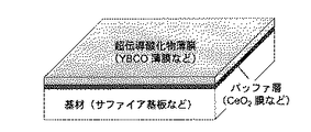
大面積超伝導薄膜、表面コート超伝導テープ線材などの大面積・長尺の高温酸化物超伝導薄膜は、限流器、超伝導送電ケーブル、超伝導マグネットなど、さまざまな電力機器や産業機器への応用が期待されている。このような応用においては、できるだけ大きな電流を抵抗ゼロで流すことが求められ、そのためには、臨界電流密度(単位断面積当りに抵抗ゼロで流すことのできる電流値)が高い、高性能の高温超伝導酸化物薄膜の作製が必須である。しかし、例えば、代表的な酸化物超伝導体である YBa2Cu3O7 (YBCO) の薄膜の場合には、サファイア(単結晶アルミナ)基板やニッケル基合金基材(テープ)などのような実用基材を用いるとき、基材と超伝導体との格子整合が悪く、かつ、基材と超伝導体とが反応するため、超伝導薄膜の直接成膜は困難で、基材と超伝導薄膜との間に格子整合と拡散防止のためのバッファ層を作製する必要がある(図1)。これまで、このようなバッファ層は、パルスレーザー蒸着法やスパッタリング法・電子ビーム蒸着法などの物理蒸着法で作製されてきた。
上記のようなパワー応用とは別に、携帯電話の基地局で使われるマイクロ波フィルターへも、大面積超伝導薄膜が応用されている。高周波デバイスに用いる超伝導薄膜では、高周波表面抵抗の値が低いことが求められ、そのためには、超伝導薄膜の表面が平滑であるほうが望ましいことが知られている。このため、超伝導薄膜を作製するためのバッファ層も、できるだけ平滑な膜が望ましいと考えられ、代表的なバッファ層である CeO2 膜について、成膜条件の探索研究が行われている。(非特許文献1 参照。)また、成膜後に、成膜温度よりもさらに高温度の熱処理を施すことによって CeO2 バッファ層が平滑化され、その上に成膜した YBCO 薄膜も表面が平滑化されるとともに高周波表面抵抗の値が低減することが報告されている。(非特許文献2参照。)しかし、この熱処理が (RE) Ba2Cu3O7 (RE = Y, Nd, Sm, Eu, Gd, Dy, Ho, Er, Yb) 薄膜(以下 (RE)BCO 薄膜と略称)の臨界電流密度に及ぼす効果については、これまで知られていない。
【非特許文献1】D. K. Develos, M. Kusunoki, M. Mukaida and S. Oshima, ”Effect of deposition rate on surface morphology of CeO2 deposited by pulsed laser deposition”, Physica C, 320, 21−30 (1999).
【非特許文献2】J. H. Lee, W. I. Yang, H. J. Kwon, V. A. Komashko and Sang Young Lee, ”Significant improvements in the surface smoothness of YBa2Cu3O7 films on high−temperature annealed CeO2−buffered r−cut sapphire”, Supercond. Sci. Technol., 13, 989 (2000).
【0003】
【発明が解決しようとする課題】
臨界電流密度の高い高温酸化物超伝導薄膜を作製するためには、マイクロクラック等がなく、かつ、粒界弱結合ができないように超伝導体を配向させる必要がある。
さらに、超伝導体の結晶性を向上させるだけでなく、量子化磁束のピン止めに有効な適当な欠陥(磁束ピン止め中心)を導入しなければならないが、高温酸化物超伝導薄膜でどの様な欠陥が有効な磁束ピン止め中心として働いているかは、多くの場合不明である。
YBCO 薄膜の場合、SrTiO3 (100) 単結晶基板が高い臨界電流密度を得るための最適基板の1つとして知られているが、この場合でも、磁束ピン止め中心の実態は不明である。このため、臨界電流密度の高い高温酸化物超伝導膜を作製するための条件は、経験的にしか明らかになっていない。
特に、実用基材に格子整合と拡散防止のためのバッファ層を用いる場合、臨界電流密度の高い膜を得るための条件は、未だ手探りの状態であった。
【0004】
【課題を解決するための手段】
発明者は、バッファ層の成膜温度よりもさらに高温度における後熱処理を施すことによってバッファ層が原子レベルで平坦化されるとともにナノメーターオーダーの表面粒子が形成され、その上に高温酸化物超伝導膜を作製すると高い臨界電流密度が得られることを発見した。
特に、高性能の超伝導酸化物が、(RE)BCO 薄膜であり、基材の上に格子整合と拡散防止のためのバッファ層(CeO2 、YSZなど)を作製し、その上に (RE)BCO 薄膜を作製する方法において、基材の上にバッファ層を成膜した後で、その成膜温度よりも高温度(900−1200℃)における後熱処理を施すことを特徴として、高い臨界電流密度を有する (RE)BCO 薄膜を作製する方法を見出した。
【0005】
【発明の実施の形態】
本発明の高い臨界電流密度を有する (RE)BCO 薄膜を作製する方法では、サファイア基板やニッケル基合金基材などの上に、格子整合と拡散防止のためのバッファ層を、従来の技術(パルスレーザー蒸着法やスパッタリング法・電子ビーム蒸着法などの物理蒸着法)で作製する。
また、本発明の高い臨界電流密度を有する (RE)BCO 薄膜を作製する方法では、従来の技術で作製した、基材・バッファ層複合体をバッファ層成膜時の温度よりもさらに高い、適当な温度で後熱処理する。
この後熱処理によって、バッファ層が原子レベルで平坦化されるとともに直径が10−20ナノメーターの表面粒子が形成される。この効果により、その上に高温酸化物超伝導膜を作製すると、後熱処理を行わない場合よりも高い臨界電流密度を得ることができる。
【0006】
本発明で用いる高性能の超伝導酸化物薄膜は、超伝導酸化物であれば、何でも良いが、代表的には(RE) Ba2Cu3O7 (RE = Y, Nd, Sm, Eu, Gd, Dy, Ho, Er, Yb)を挙げることができる。
また、格子整合と拡散防止のためのバッファ層は、CeO2 、Y2O3 、YSZ(イットリア安定化ジルコニア)など(あるいはその組合せ)が適している。
さらに、基材としては、サファイヤ、ニッケル金属、ニッケル基合金(ハステロイ、インコネル等)、ステンレス系合金などがある。
また、基材・バッファ層複合体の後熱処理は、通常バッファ層成膜時の温度よりも高い800〜1300℃とくに、900〜1200℃で行うと良い。後熱処理温度の処理時間は、0.5〜3時間程度が望ましい。とくに、1〜1.5時間で行うと良い。
【0007】
本発明について実施例を用いてさらに詳しく説明するが、本発明はこれら実施例に限定されるものではない。
(実施例1)
(基材・バッファ層の形成)
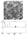
図2は、R面サファイア単結晶基板の上にパルスレーザー蒸着法で作製した、CeO2 バッファ層の原子間力顕微鏡像と、図の直線上の凹凸のプロファイルを示す。図2から、表面は平坦でなく、約 10 nm の凹凸があることがわかった。
(基材・バッファ層の後熱処理)
この CeO2 バッファ層を酸素気流中で 1000℃、1時間熱処理を行ったところ、図3に示すような、原子レベルで平坦な表面を得ることができた。この場合の表面の凹凸は、1nm 以下にまで減少した。また、直径が10−20ナノメーターの表面粒子が形成された。
(基材・バッファ層・超伝導膜複合体の形成)
このCeO2 バッファ層の上に、超伝導体である YBa2Cu3O7 (YBCO) の薄膜をパルスレーザー蒸着法により成膜した。成膜条件は、基板温度 730℃、酸素300 mTorr、レーザー強度は約4J/cm2、繰返し周波数5Hz であった。
【0008】
(基材・バッファ層・超伝導膜複合体の比較例1)
実施例1と同じ基材・バッファ層を作製し、バッファ層を後熱処理しないでその上に、超伝導体である YBa2Cu3O7 (YBCO) の薄膜をパルスレーザー蒸着法により実施例1と同一条件で成膜した。
【0009】
(実施例1及び比較例1の臨界電流密度テスト)
実施例1で作製した基材・バッファ層・超伝導膜複合体及び比較例1の基材・バッファ層・超伝導膜複合体について、幅40μm、長さ2mmのブリッジを形成し、極低温容器中で測定温度を変化させながら、パルス電流を用いた通電法によって臨界電流密度を測定した。
図4に示すように、後熱処理の効果によって、実施例1のものは比較例1に比して、臨界電流密度が2〜10倍に向上した。この臨界電流密度は、SrTiO3 単結晶基板上に同様な条件で作製した YBCO 膜の臨界電流密度と同等か、それ以上であった。
【0010】
【本発明の効果】
本願発明によって、高性能 (RE)BCO 薄膜の作製に必要なバッファ層を原子レベルで平坦化するとともに、直径が10−20ナノメーターの表面粒子を形成させることに成功した。これにより、従来知られていた最適基板と同等かそれ以上の臨界電流密度を有する (RE)BCO 薄膜を作製することができる。
【図面の簡単な説明】
【図1】基材、バッファ層、超伝導膜の関係を示す模式図。
【図2】R面サファイア単結晶基板の上に作製した、CeO2 バッファ層の原子間力顕微鏡像と、表面の凹凸のプロファイル。
【図3】第2図の CeO2 バッファ層を、成膜時よりもさらに高温度において後熱処理することによって得られた、原子レベルで平坦なバッファ層の原子間力顕微鏡像と、表面の凹凸のプロファイル。
【図4】(黒丸)後熱処理なしのバッファ層の上に成膜した YBCO 薄膜の臨界電流密度の温度依存性。(白丸)後熱処理によって原子レベルで平坦化されたバッファ層の上に成膜した YBCO 薄膜の臨界電流密度の温度依存特性図。[0001]
TECHNICAL FIELD OF THE INVENTION
The present invention relates to a method for producing a high-temperature oxide superconductor having a large area, a long length, and a high critical current, such as a large-area superconducting film and a surface-coated superconducting tape wire.
[0002]
[Prior art]
Large-area, long high-temperature oxide superconducting thin films, such as large-area superconducting thin films and surface-coated superconducting tape wires, are used in a variety of power and industrial equipment, such as current limiters, superconducting power transmission cables, and superconducting magnets. The application of is expected. In such applications, it is required that a current as large as possible flows at zero resistance. To achieve this, a high-performance high-temperature high critical current density (a current value that can flow at zero resistance per unit cross-sectional area) is high. Preparation of a superconducting oxide thin film is essential. However, for example, in the case of a thin film of YBa 2 Cu 3 O 7 (YBCO) which is a typical oxide superconductor, such as a sapphire (single crystal alumina) substrate and a nickel-based alloy base material (tape) When a practical substrate is used, the lattice matching between the substrate and the superconductor is poor, and the substrate and the superconductor react with each other, making it difficult to form a superconducting thin film directly. It is necessary to form a buffer layer for lattice matching and diffusion prevention between the thin film (FIG. 1). Heretofore, such a buffer layer has been produced by a physical vapor deposition method such as a pulse laser vapor deposition method, a sputtering method, and an electron beam vapor deposition method.
Apart from the above power applications, large-area superconducting thin films are also applied to microwave filters used in base stations of mobile phones. A superconducting thin film used for a high-frequency device is required to have a low high-frequency surface resistance, and it is known that a smooth surface of the superconducting thin film is more desirable for that purpose. For this reason, it is considered that a buffer layer for producing a superconducting thin film is also desirably as smooth as possible, and a search for film formation conditions for a CeO 2 film, which is a typical buffer layer, is being conducted. (See Non-Patent Document 1.) After the film formation, the CeO 2 buffer layer is smoothed by performing a heat treatment at a temperature higher than the film formation temperature, and the surface of the YBCO thin film formed thereon is also smoothed. And it is reported that the value of the high-frequency surface resistance is reduced. (Refer to Non-Patent
[Non-Patent Document 1] K. Develos, M .; Kusunoki, M .; Mukaida and S.M. Oshima, "Effect of deposition rate on surface morphology of CeO 2 deposited by pulsed laser deposition", Physica C, 320, 19-30.
[Non-Patent Document 2] H. Lee, W.C. I. Yang, H .; J. Kwon, V .; A. Komashko and Sang Young Lee, "Significant improvements in the surface smoothness of YBa 2 Cu 3 O 7 films on high-temperature annealed CeO 2 -buffered r-cut sapphire", Supercond. Sci. Technol. , 13, 989 (2000).
[0003]
[Problems to be solved by the invention]
In order to produce a high-temperature oxide superconducting thin film having a high critical current density, it is necessary to orient the superconductor without microcracks and the like, and to prevent weak bonding at grain boundaries.
Furthermore, it is necessary to not only improve the crystallinity of the superconductor, but also to introduce an appropriate defect effective for pinning the quantized magnetic flux (flux pinning center). It is often unclear whether such defects serve as effective flux pinning centers.
In the case of a YBCO thin film, a SrTiO 3 (100) single crystal substrate is known as one of the optimal substrates for obtaining a high critical current density, but even in this case, the actual state of the magnetic flux pinning center is unknown. Therefore, conditions for producing a high-temperature oxide superconducting film having a high critical current density have been clarified only by experience.
In particular, when a buffer layer for lattice matching and diffusion prevention is used for a practical base material, the conditions for obtaining a film having a high critical current density are still groping.
[0004]
[Means for Solving the Problems]
The inventor of the present invention has performed a post-heat treatment at a temperature higher than the film formation temperature of the buffer layer, thereby flattening the buffer layer at the atomic level and forming nanometer-order surface particles. It has been found that a high critical current density can be obtained by fabricating a conductive film.
In particular, a high-performance superconducting oxide is a (RE) BCO 3 thin film, and a buffer layer (CeO 2 , YSZ, etc.) for lattice matching and diffusion prevention is formed on a substrate, and (RE) is formed thereon. A method for producing a BCO thin film, characterized in that after forming a buffer layer on a base material, a post-heat treatment at a temperature (900-1200 ° C.) higher than the film forming temperature is performed. A method for producing a (RE) BCO 3 thin film having a high density has been found.
[0005]
BEST MODE FOR CARRYING OUT THE INVENTION
In the method of producing a (RE) BCO thin film having a high critical current density according to the present invention, a buffer layer for lattice matching and diffusion prevention is formed on a sapphire substrate or a nickel-based alloy substrate by a conventional technique (pulse It is produced by a physical vapor deposition method such as a laser vapor deposition method, a sputtering method, and an electron beam vapor deposition method.
In the method for producing a (RE) BCO 3 thin film having a high critical current density according to the present invention, the temperature of the substrate / buffer layer composite produced by the conventional technique is higher than the temperature at the time of forming the buffer layer. Post heat treatment at a suitable temperature.
Subsequent heat treatment flattens the buffer layer at the atomic level and forms surface particles with a diameter of 10-20 nanometers. Due to this effect, when a high-temperature oxide superconducting film is formed thereon, a higher critical current density can be obtained than when no post-heat treatment is performed.
[0006]
The high-performance superconducting oxide thin film used in the present invention is not particularly limited as long as it is a superconducting oxide. Typically, (RE) Ba 2 Cu 3 O 7 (RE = Y, Nd, Sm, Eu, Gd, Dy, Ho, Er, Yb).
As the buffer layer for lattice matching and diffusion prevention, CeO 2 , Y 2 O 3 , YSZ (yttria stabilized zirconia), or the like (or a combination thereof) is suitable.
Further, examples of the base material include sapphire, nickel metal, nickel-based alloys (such as Hastelloy and Inconel), and stainless steel alloys.
Further, the post heat treatment of the base material / buffer layer composite is preferably performed at 800 to 1300 ° C., particularly 900 to 1200 ° C., which is higher than the temperature at the time of forming the buffer layer. The post-heat treatment time is desirably about 0.5 to 3 hours. In particular, it is good to perform it in 1 to 1.5 hours.
[0007]
The present invention will be described in more detail with reference to examples, but the present invention is not limited to these examples.
(Example 1)
(Formation of base material / buffer layer)
FIG. 2 shows an atomic force microscope image of a CeO 2 buffer layer formed on a R-plane sapphire single crystal substrate by a pulsed laser deposition method and a profile of unevenness on a straight line in the drawing. From FIG. 2, it was found that the surface was not flat and had irregularities of about 10 nm.
(Post-heat treatment of substrate / buffer layer)
When this CeO 2 buffer layer was subjected to heat treatment at 1000 ° C. for 1 hour in an oxygen stream, a flat surface at an atomic level as shown in FIG. 3 could be obtained. In this case, the surface irregularities were reduced to 1 nm or less. Also, surface particles having a diameter of 10-20 nanometers were formed.
(Formation of substrate / buffer layer / superconducting membrane composite)
A thin film of YBa 2 Cu 3 O 7 (YBCO), which is a superconductor, was formed on the CeO 2 buffer layer by a pulsed laser deposition method. The film formation conditions were a substrate temperature of 730 ° C., oxygen of 300 mTorr, a laser intensity of about 4 J / cm 2 , and a repetition frequency of 5 Hz.
[0008]
(Comparative example 1 of base material / buffer layer / superconducting film composite)
The same base material / buffer layer as in Example 1 was manufactured, and a thin film of YBa 2 Cu 3 O 7 (YBCO), which is a superconductor, was formed on the buffer layer without pulsed heat treatment by pulse laser deposition. The film was formed under the same conditions as in
[0009]
(Critical current density test of Example 1 and Comparative Example 1)
With respect to the substrate / buffer layer / superconducting film composite prepared in Example 1 and the substrate / buffer layer / superconducting film composite of Comparative Example 1, a bridge having a width of 40 μm and a length of 2 mm was formed, and a cryogenic container was prepared. The critical current density was measured by an energization method using a pulse current while changing the measurement temperature in the inside.
As shown in FIG. 4, the critical current density of Example 1 was improved 2 to 10 times as compared with Comparative Example 1 due to the effect of the post heat treatment. This critical current density was equal to or higher than the critical current density of the YBCO film formed on the SrTiO 3 single crystal substrate under the same conditions.
[0010]
[Effects of the present invention]
According to the present invention, the buffer layer required for producing a high-performance (RE) BCO thin film has been flattened at an atomic level, and surface particles having a diameter of 10 to 20 nanometers have been successfully formed. As a result, a (RE) BCO thin film having a critical current density equal to or higher than the conventionally known optimum substrate can be produced.
[Brief description of the drawings]
FIG. 1 is a schematic diagram showing a relationship between a base material, a buffer layer, and a superconducting film.
FIG. 2 shows an atomic force microscope image of a CeO 2 buffer layer and a profile of surface irregularities, which are formed on an R-plane sapphire single crystal substrate.
FIG. 3 shows an atomic force microscope image of an atomically flat buffer layer obtained by post-heating the CeO 2 buffer layer of FIG. 2 at a higher temperature than at the time of film formation, and surface irregularities. Profile.
FIG. 4 (black circles) Temperature dependence of critical current density of YBCO thin film formed on buffer layer without post-heat treatment. (Open circles) Temperature dependence of critical current density of YBCO thin film formed on buffer layer flattened at atomic level by post heat treatment.
Claims (4)
Priority Applications (1)
| Application Number | Priority Date | Filing Date | Title |
|---|---|---|---|
| JP2003035361A JP4852693B2 (en) | 2003-02-13 | 2003-02-13 | Preparation method of superconducting oxide thin film with high critical current density |
Applications Claiming Priority (1)
| Application Number | Priority Date | Filing Date | Title |
|---|---|---|---|
| JP2003035361A JP4852693B2 (en) | 2003-02-13 | 2003-02-13 | Preparation method of superconducting oxide thin film with high critical current density |
Publications (2)
| Publication Number | Publication Date |
|---|---|
| JP2004244263A true JP2004244263A (en) | 2004-09-02 |
| JP4852693B2 JP4852693B2 (en) | 2012-01-11 |
Family
ID=33020804
Family Applications (1)
| Application Number | Title | Priority Date | Filing Date |
|---|---|---|---|
| JP2003035361A Expired - Lifetime JP4852693B2 (en) | 2003-02-13 | 2003-02-13 | Preparation method of superconducting oxide thin film with high critical current density |
Country Status (1)
| Country | Link |
|---|---|
| JP (1) | JP4852693B2 (en) |
Cited By (5)
| Publication number | Priority date | Publication date | Assignee | Title |
|---|---|---|---|---|
| JP2007109717A (en) * | 2005-09-14 | 2007-04-26 | Sharp Corp | Superconducting element and its fabrication process |
| KR100801639B1 (en) | 2006-09-20 | 2008-02-05 | 한국전기연구원 | Diffusion barrier layer and the hts tape using refractory metal and ceramic mixed layer |
| US8105981B2 (en) * | 2007-09-20 | 2012-01-31 | Kabushiki Kaisha Toshiba | Superconducting member |
| WO2012165563A1 (en) * | 2011-05-31 | 2012-12-06 | 古河電気工業株式会社 | Oxide superconductor thin film and superconducting fault current limiter |
| JP2013006759A (en) * | 2011-05-23 | 2013-01-10 | Furukawa Electric Co Ltd:The | Oxide superconducting thin film |
Citations (1)
| Publication number | Priority date | Publication date | Assignee | Title |
|---|---|---|---|---|
| JPH0597590A (en) * | 1991-10-08 | 1993-04-20 | Sumitomo Cement Co Ltd | Production of oxide high-temperature superconducting thin film and optical element using the same |
-
2003
- 2003-02-13 JP JP2003035361A patent/JP4852693B2/en not_active Expired - Lifetime
Patent Citations (1)
| Publication number | Priority date | Publication date | Assignee | Title |
|---|---|---|---|---|
| JPH0597590A (en) * | 1991-10-08 | 1993-04-20 | Sumitomo Cement Co Ltd | Production of oxide high-temperature superconducting thin film and optical element using the same |
Cited By (7)
| Publication number | Priority date | Publication date | Assignee | Title |
|---|---|---|---|---|
| JP2007109717A (en) * | 2005-09-14 | 2007-04-26 | Sharp Corp | Superconducting element and its fabrication process |
| KR100801639B1 (en) | 2006-09-20 | 2008-02-05 | 한국전기연구원 | Diffusion barrier layer and the hts tape using refractory metal and ceramic mixed layer |
| US8105981B2 (en) * | 2007-09-20 | 2012-01-31 | Kabushiki Kaisha Toshiba | Superconducting member |
| JP2013006759A (en) * | 2011-05-23 | 2013-01-10 | Furukawa Electric Co Ltd:The | Oxide superconducting thin film |
| WO2012165563A1 (en) * | 2011-05-31 | 2012-12-06 | 古河電気工業株式会社 | Oxide superconductor thin film and superconducting fault current limiter |
| JPWO2012165563A1 (en) * | 2011-05-31 | 2015-02-23 | 古河電気工業株式会社 | Oxide superconducting thin film and superconducting fault current limiter |
| US9159898B2 (en) | 2011-05-31 | 2015-10-13 | Furukawa Electric Co., Ltd. | Oxide superconductor thin film and superconducting fault current limiter |
Also Published As
| Publication number | Publication date |
|---|---|
| JP4852693B2 (en) | 2012-01-11 |
Similar Documents
| Publication | Publication Date | Title |
|---|---|---|
| JP5806302B2 (en) | Multifilament superconductor with reduced AC loss and its formation method | |
| US6383989B2 (en) | Architecture for high critical current superconducting tapes | |
| JP4041672B2 (en) | Bonding high temperature superconducting coated tape | |
| JP3587956B2 (en) | Oxide superconducting wire and its manufacturing method | |
| US6730410B1 (en) | Surface control alloy substrates and methods of manufacture therefor | |
| JP2007532775A (en) | Biaxially oriented film deposition for superconductor coated tapes | |
| AU2007252693A1 (en) | Superconducting thin film material and method of manufacturing the same | |
| US6884527B2 (en) | Biaxially textured composite substrates | |
| JP5799081B2 (en) | Thick oxide film with single layer coating | |
| KR20080041665A (en) | Structure for improved high critical current densities in ybco coatings | |
| WO2011099301A1 (en) | Oxide superconductor cabling and method of manufacturing oxide superconductor cabling | |
| WO2007040567A2 (en) | Method for improving performance of high temerature superconductors within a magnetic field | |
| JP2002150855A (en) | Oxide superconductor wire material, and manufacturing method of the same | |
| JP4891505B2 (en) | Methods and compositions for making multilayer bodies | |
| JP4852693B2 (en) | Preparation method of superconducting oxide thin film with high critical current density | |
| JP5686437B2 (en) | Oxide superconducting thin film wire and method for producing the same | |
| JPWO2004088677A1 (en) | Metal substrate for oxide superconducting wire, oxide superconducting wire, and manufacturing method thereof | |
| JP5881107B2 (en) | Method for introducing nanoscale crystal defects into high temperature superconducting oxide thin films | |
| JP5415824B2 (en) | Method for manufacturing a substrate with altered shape for coated conductor and coated conductor using said substrate | |
| JPH10125148A (en) | Oxide superconductor complex and its manufacture | |
| JP2012022882A (en) | Base material for oxide superconducting conductor and method of manufacturing the same, and oxide superconducting conductor and method of manufacturing the same | |
| Haugan et al. | Addition of alternate phase nanoparticle dispersions to enhance flux pinning of Y-Ba-Cu-O thin films | |
| JP6359328B2 (en) | RE123 crystal film production method. | |
| Mancini et al. | MgO/TiN buffer layer structures for coated conductor development on Cu-based substrates | |
| JP2011249162A (en) | Method for manufacturing superconducting wire rod |
Legal Events
| Date | Code | Title | Description |
|---|---|---|---|
| A621 | Written request for application examination |
Free format text: JAPANESE INTERMEDIATE CODE: A621 Effective date: 20041124 |
|
| A977 | Report on retrieval |
Free format text: JAPANESE INTERMEDIATE CODE: A971007 Effective date: 20070402 |
|
| A131 | Notification of reasons for refusal |
Free format text: JAPANESE INTERMEDIATE CODE: A131 Effective date: 20080205 |
|
| A521 | Request for written amendment filed |
Free format text: JAPANESE INTERMEDIATE CODE: A523 Effective date: 20080324 |
|
| A02 | Decision of refusal |
Free format text: JAPANESE INTERMEDIATE CODE: A02 Effective date: 20080715 |
|
| A521 | Request for written amendment filed |
Free format text: JAPANESE INTERMEDIATE CODE: A523 Effective date: 20080911 |
|
| A911 | Transfer to examiner for re-examination before appeal (zenchi) |
Free format text: JAPANESE INTERMEDIATE CODE: A911 Effective date: 20081028 |
|
| A912 | Re-examination (zenchi) completed and case transferred to appeal board |
Free format text: JAPANESE INTERMEDIATE CODE: A912 Effective date: 20081226 |
|
| A521 | Request for written amendment filed |
Free format text: JAPANESE INTERMEDIATE CODE: A821 Effective date: 20110421 |
|
| A521 | Request for written amendment filed |
Free format text: JAPANESE INTERMEDIATE CODE: A523 Effective date: 20110721 |
|
| A01 | Written decision to grant a patent or to grant a registration (utility model) |
Free format text: JAPANESE INTERMEDIATE CODE: A01 |
|
| R150 | Certificate of patent or registration of utility model |
Ref document number: 4852693 Country of ref document: JP Free format text: JAPANESE INTERMEDIATE CODE: R150 Free format text: JAPANESE INTERMEDIATE CODE: R150 |
|
| S533 | Written request for registration of change of name |
Free format text: JAPANESE INTERMEDIATE CODE: R313533 |
|
| R350 | Written notification of registration of transfer |
Free format text: JAPANESE INTERMEDIATE CODE: R350 |
|
| EXPY | Cancellation because of completion of term |