【0001】
【発明の属する技術分野】
本発明は、新規な構造のユニモルフ型インクジェットヘッド、及び該インクジェットヘッドを得るための製造方法である。更に詳しくは、仕様の変更に容易に対応可能なインクジェットヘッドおよびその製造方法である。
【0002】
【従来の技術】
近年、光学や精密加工等の分野において、サブミクロンのオーダーで光路長や位置を調整する変位素子や微小変位を電気的変化として検知する検出素子が所望されるようになってきており、これに応えるものとして、強誘電体を用いた圧電・電歪材料に電界を加えた時に起こる逆圧電効果や電歪効果に基づくところの変位あるいは、その逆の現象を利用した素子である、アクチュエーターやセンサーの如き圧電・電歪素子の開発が進められている。
【0003】
ところで、インクジェットプリントヘッド等においては、そのような圧電・電歪素子構造として、従来から知られているユニモルフ型が好適に採用されている。そして、そこでは、そのような素子を用いたプリンターの印字品質・印字速度等の向上が要求されており、それに応えるべく、かかる圧電・電歪膜型素子の小型高密度化、低電圧駆動化、高速応答性化、長尺多ノズル化を図るための開発が進められている。
【0004】
それらの克服のために、特許文献1には、圧電スピーカーとして、圧電セラミックスとセラミックス振動板を同時に焼結することで強固な接合強度をもたらす技術が開示されている。また、特許文献2には、シリコン基板上にゾルゲル法あるいはスパッタ法で圧電膜を成膜し、インクジェットヘッドを製造する方法が記載されている。この方法は、シリコン基板を加工し、個別液室(圧力室)を形成し、ヘッドを得る方法である。
【0005】
また、特許文献3には、インク流路が形成された基板と、ノズルを有するノズル板からなるインクジェットヘッドにおいて、ノズルのインク吐出口の穴径が小さく形成され、流路と連通する側の穴径が流路の径よりも大きく形成されたインクジェットヘッドが記載されている。特許文献4には、基板上に圧電膜を形成したのち、これを下部電極に転写する工程を用いて圧電膜型アクチュエーターを製造する方法が記載されている。
【0006】
【特許文献1】
特開昭62−213399号公報
【特許文献2】
米国特許第5265315号明細書
【特許文献3】
特開平3−297651号公報
【特許文献4】
特開2002−134806号公報
【0007】
【発明が解決しようとする課題】
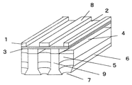
図1には、ユニモルフ型インクジェットヘッドの従来例の断面図を示した。図中、1は圧電・電歪膜、2は下部電極、3は振動板、4は個別液室、6はノズル7が形成されたノズルプレートである。インクジェットヘッドのノズルを高密度化するためには、個別液室4の幅及び隔壁9の幅を小さくする必要があり、それらが小さくなっても液滴が吐出するだけの十分な変位量が必要である。
このような方法により高密度化した、ユニモルフ型の圧電・電歪素子においては、大きな屈曲変位や発生力を得るために、振動板3となる基板の厚さを薄くすることが重要とされるが、かかる基板の厚さを減少させると、強度が低下する、厚みムラの影響のためにばらつきが大きくなるという問題が生じる場合があった。
【0008】
特許文献1の方法では圧電体と振動板を強固な接合強度で接合することが可能であるが、この方法は高温で異種の材料を焼結することから、振動板及び圧電セラミックスそのものが収縮し、大面積での作成を行う場合にはミクロンオーダーの寸応精度を合わせることが困難な場合があった。
【0009】
また、特許文献2の方法では、シリコン基板の厚みが個別液室の深さとなり、必要な吐出液滴量や吐出圧力に適応良く対応することが出来ない場合があった。例えば、基板サイズが6インチの場合の汎用品の厚みは500〜700μmであり、8インチの場合は、600〜800μmである。これらの基板を用いて、個別液室を作製する場合、この基板の厚みが個別液室の深さとなり、吐出液滴量の設定等のヘッドスペック上、好ましくない場合が発生する。また、基板を研磨等で薄膜化し対応した場合、研磨による厚みむらによりヘッドの長尺化に対応出来ない等の問題が生じる場合あった。特許文献3に記載のインクジェットヘッドでは、ノズルプレートと連通孔基板との間で気泡が溜る場合がある。
【0010】
本発明の目的は、上記問題点を解決したユニモルフ型のアクチュエーター及びインクジェットヘッドを提供することにある。また、本発明の他の目的は、多ノズルで信頼性の高いアクチュエーター及びインクジェットヘッドを提供することにある。即ち、低駆動電圧で大変位が得られ、応答速度が速く、発生力の大きい、多ノズル化・高集積化が可能であるアクチュエーター・インクジェットヘッドを提供することにある。また本発明の他の目的は、隔壁部の剛性が高く、個別液室の深さを200μm以下に浅く出来、液滴の吐出スピードに優れたインクジェットヘッドを提供することにある。
【0011】
【課題を解決するための手段】
本発明のインクジェットヘッドは、吐出口に連通する個別液室、振動板および圧電・電歪素子を有するユニモルフ型インクジェットヘッドにおいて、前記個別液室の内壁の一部を振動板を有する振動部として形成し、前記圧電・電歪素子を該振動部上の該個別液室側に配置したことを特徴とする。すなわち、本発明のインクジェットヘッドは、圧電・電歪素子より下部に振動板が、圧電・電歪素子より上部に個別液室の少なくとも一部が位置する構成を有するものである。ここで、個別液室、圧電・電歪素子および振動板の位置関係は、インクの吐出方向を基準にして、ノズル側を上、基板側を下とする方向を基準としたものである。「圧電・電歪素子より下部に振動板」を有するとは、振動板の最も上の面が圧電・電歪素子の最も下の面よりも下にあることを表す。また、「圧電・電歪素子より上部に個別液室の少なくとも一部が位置する」とは、個別液室の最も上の面が圧電・電歪素子の最も下の面よりも上にあることを表す。
【0012】
本発明によれば、圧電・電歪素子を個別液室側に入れたことにより、圧電・電歪素子での圧力発生が、振動板及び圧電・電歪素子を支持する基板の厚みに影響されなくなり、かつ個別液室及び圧電・電歪素子の幅の低減化も容易となり、個別液室の寸法制度が高く、特性ばらつきも少なく、更にノズルの高密度化に好適な構造を有するインクジェットヘッドを得ることが出来る。
【0013】
【発明の実施の形態】
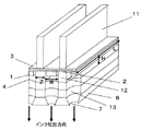
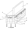
本発明のインクジェットヘッドの主要部を、4つの側面を断面として表した模式的斜視図(図2及び図4)に示した。すなわち図2及び図4は、ヘッドの正面側、背面側及び左右両側面を断面として表わしており、また、吐出口を有するノズルが下方に向いている状態の斜視図となっている。これらの図中、11は基板であり、振動板3まで部分的にエッチング加工されている。基板の加工により残された部分11は、図2の構成では一個の個別液室に一個対応しているが、図4の構成では、複数個の個別液室に対して一個対応している。11の上に振動板3と下部電極2が形成されている。振動板3は基板の一部として形成されたものであっても良いし、基板上に新たに成膜された膜あるいは接合された膜であっても良い。振動板3と下部電極2との積層体が個別液室4の内壁を構成している部分は振動板に基づく振動部となっており、この振動部上に圧電・電歪膜1が配置されている。圧電・電歪膜1の上面には上部電極(不図示)が設けられており、下部電極の圧電・電歪膜1の下の領域とこの上部電極で、圧電・電歪膜1を挟持した構成を有する圧電・電歪素子が構成されている。
【0014】
このインクジェットヘッドでは、振動板の面方向に対して垂直方向に中心軸を有する下端に吐出口を有するノズルが伸びて、吐出口の開口面と振動板の面とが平行に位置するようになっている。この構成により、個別液室の長手方向と直行するノズルの下端に位置する吐出口から振動板の面方向と直行する方向に液体が吐出する。この液体の吐出方向を図中に示した。
【0015】
本発明によれば、圧電・電歪素子を個別液室側に入れたことにより、圧電・電歪素子での圧力発生が、振動板及び圧電・電歪素子を支持する基板の厚みに影響されなくなり、かつ個別液室及び圧電・電歪素子の幅の低減化も容易となり、個別液室の寸法制度が高く、特性ばらつきも少なく、更にノズルの高密度化に好適な構造を有するインクジェットヘッドを得ることが出来る。
【0016】
個別液室4の深さは、個別液室プレート12の厚みで調整することが出来る。本発明のインクジェットヘッドの圧電・電歪膜1は下部電極2と上部電極(不図示)の一対の電極間に圧電・電歪膜を挟持されていることが好ましい。図示した構成のように、下部電極2からなる面の所定部に圧電・電歪膜を設け、その上部に更に上部電極を設けて、例えば下部電極を共通電極として、上部電極を選択(駆動)電極として利用することで、画像デジタル情報を高精度に圧電・電歪膜に伝達することができる。
【0017】
上部電極及び下部電極のうちの個別液室と接する部分は液体に対する耐性を有する材料から構成される。例えば、電極の液体と接する面にパッシベーション膜を形成することで液体に対する耐性を電極に付与することができる。
上記の構成のインクジェットヘッドは、例えば、吐出口に連通する個別液室、振動板および圧電・電歪素子を有するユニモルフ型インクジェットヘッドの製造方法において、
基板の振動板となる部分に下部電極を形成する工程と、
該下部電極上に圧電・電歪膜を形成する工程と、
該圧電・電歪膜上に上部電極を形成して圧電・電歪素子とする工程と、
該圧電・電歪素子の少なくとも一部を内包する個別液室を形成する工程と、
該個別液室に連通し、吐出口を有するノズルを形成する工程と、
を有することを特徴とするインクジェットヘッドの製造方法により製造する事が出来る。
【0018】
特に、本発明の基板は、シリコン基板、SOI基板(silicon on insulator)あるいはSOS基板(silicon on sapphire)が好ましい。これらの基板を使用することによって、低駆動電圧で変位が大きく、機械的強度が高く、膜厚均一性に優れた振動板を得ることができる。本発明の振動板の形成方法は、上記基板のドライエッチング及びウェットエッチングの少なくとも一つの方法によることが好ましい。また、本発明の振動板の形成方法は、薄膜プロセスによる方法によることが好ましい。
【0019】
本発明のインクジェットヘッドの各構成要素について更に詳説する。
圧電・電歪膜の厚み(インク吐出方向における厚さ)は、1μm以上30μm以下が好ましく、1μm以上10μm以下がより好ましい。振動板の厚みは、1μm以上30μm以下が好ましく、より好ましくは、1μm以上10μm以下である。個別液室の幅(図2及び4のW、個別液室プレート間の間隔)は、任意に設定出来るが、30μm以上500μm以下が好ましく、より好ましくは、30μm以上150μm以下である。
【0020】
個別液室の長さ(図2及び4のL、ノズルの中心軸に直行する方向での、個別液室の内壁面(ノズルの中心軸に平行な面)の間の距離。)は、任意に設定出来るが、50μm以上6000μm以下が好ましく、より好ましくは300μm以上3000μm以下である。個別液室の深さ(図2及び4のH、インク吐出方向の長さ)は、任意に設定出来るが、30μm以上400μm以下が好ましく、より好ましくは50μm以上200μm以下である。ノズルは、その中心軸に垂直な断面を円や星型、三角形、四角形などとした形状を採ることが出来るが、好ましくは、かかる断面が円、星型である。断面が円形の場合のノズル径は5μm以上50μm以下が好ましく、より好ましくは、7μm以上30μm以下である。
【0021】
また、個別液室とノズルを繋げる連通孔13が設けられることが好ましい。図2の模式図は、ノズルプレート6の上に2枚の板材を利用して連通孔が形成された例であるが、連通孔が無い場合でも良い。図2は、さらに個別液室が形成された板材と振動板等が設けられた基板とからなる例である。連通孔13の径はノズル径より大きい。ノズルはノズルプレート間でテーパー形状を有しているのが好ましく、ノズル径が10〜30μmである場合、連通孔側の穴径は15〜60μmが好ましい。
【0022】
ノズルプレート6の厚みは、30μm以上150μm以下であることが好ましい。連通孔のインク吐出方向における長さは、30μm以上300μm以下であることが好ましい。ノズルプレート6は、更に図3の断面図に示されるように一つの基材内にノズル7と連通孔13が形成されたものであっても良い。
【0023】
連通孔部、ノズル部の作成方法としては、各穴を形成した基材を接合する方法、あるいは各部分を電鋳、メッキ、蒸着、射出成型等の方法で作製する方法が採れる。穴を形成する基材としては、シリコン基材、SUS基材、Ni基材、ポリマー材料やカーボン材料、カーボンやシリカを含んだ複合材料等がある。電鋳、メッキ、蒸着等の方法による場合は、穴あるいは凹部を形成する部分が、レジスト、あるいはマスク等を利用したパターニングによって形成されるように成膜を行なう。ノズル部、連通孔部を形成する板材の好ましいヤング率は、0.1GPa以上である。0.1GPa以上のとき、隔壁部が薄くなっても振動板/圧電・電歪素子を含む構成におけるアクチュエータ部の変位に対して隔壁部が変位せず、吐出性能が低下しない。
【0024】
本発明で呼称する圧電・電歪膜とは、圧電膜および/または電歪膜の意味である。圧電・電歪膜に用いられる材料としては、ペロブスカイト型化合物が挙げられる。例えば、チタン酸ジルコン酸鉛PZT[Pb(ZrxTi1−x)O3]やチタン酸バリウムBaTiO3などの圧電材料やリラクサ系材料の電歪材料がある。チタン酸ジルコン酸鉛(PZT)のxは0.40から0.65のMPB(morphotropic phase boundary)組成が好ましいが、それ以外の組成比でも良い。PZTの結晶構造は正方晶、菱面体晶のいずれの結晶構造でも良い。BaTiO3は、正方晶で(001)配向された膜が好ましい。また、BaTiO3は微量の鉛、ビスマスが含有されていても良い。
【0025】
本発明で使用する電歪材料としては以下の物が選択出来る。例えば、PMN[Pb(MgxNb1−x)O3]、PNN[Pb(NbxNi1−x)O3]、PSN[Pb(ScxNb1−x)O3]、PZN[Pb(ZnxNb1−x)O3]、PMN−PT{(1−y)[Pb(MgxNb1−x)O3]−y[PbTiO3]}、PSN−PT{(1−y)[Pb(ScxNb1−x)O3]−y[PbTiO3]}、PZN−PT{(1−y)[Pb(ZnxNb1−x)O3]−y[PbTiO3]}、LN[LiNbO3]、KN[KNbO3]である。
【0026】
ここで、xおよびyは1以下で0以上の数である。例えば、PMNの場合xは0.2〜0.5、PNNの場合xは0.2〜0.5、PSNではxは0.4〜0.7、PZNの場合xは0.1〜0.5、PMN−PTのyは0.2〜0.4、PSN−PTのyは0.35〜0.5、PZN−PTのyは0.03〜0.35が好ましい。また、PMN−PT、PZN−PT、PNN−PT、PSN−PTにZrがTiの一部に代替されて含まれたPMN−PZT、PZN−PZT、PNN−PZT、PSN−PZT化合物であっても良い。
【0027】
圧電・電歪膜は単一組成であっても良いし、2種類以上の組み合わせでも良い。又、上記主成分に微量の元素をドーピングした組成物であっても良い。本発明の圧電・電歪膜は、優れた圧電性を発現するために、圧電・電歪膜は結晶制御されたものが良く、X線回折で特定の結晶構造の特定の方位が50%以上あるものが好ましく、さらには、90%以上のものがより好ましい。又、圧電・電歪膜の結晶粒径の大きさは、0.02μm以上が好ましい。結晶粒径は、粒状でも良く、膜厚方向に流い島状であっても良い。また、単結晶膜においては、上記結晶粒径の大きさは、視認出来ない場合もある。
【0028】
電極材料としては、金属や導電性金属酸化物が用いられる。金属としては、例えば、Pt,Au,Ni,Ir,Os,Cr、SUSなどである。導電性金属酸化物としては、好ましくは、ペロブスカイト型化合物で、例えば、SrRuO3,Laドープ−SrTiO3、Laドープ−SrCoO3、Nbドープ−SrTiO3、BaPbO3、LaNiO3、LaCrO3、CaRuO3などである。上部電極と下部電極材料は、異種材料であっても、同じ材料であっても良い。また、電極の下部に接着性向上のためにアンカー層を有していても良い。アンカー層としては、例えば、Ti、Cr、Pb、Ir等の金属材料やTiO2、IrO等の金属酸化物が用いられる。電極の膜厚は、0.05〜1.0μmが好ましく、より好ましくは、0.1〜0.3μmである。
【0029】
振動板材料としては、後述するように選択する製造方法により変わるが、Si、SiO2、YSZ,PSZ、ZrO2等や、あるいは電極が振動板を兼ねても良い。電極が振動板を兼ねる場合には、電極の厚みは、上記範囲ではなく、0.5μm〜6μmであることが好ましい。振動板の好ましいヤング率としては、10〜300GPaである。例えば、Si基板を振動板として用いた場合は、100〜160GPaである。
【0030】
次に、各先に挙げた工程を有する本発明のインクジェットヘッドの製造方法について更に説明する。本発明のインクジェットヘッドは、振動板及び/又は圧電・電歪膜の厚みが1μm以上30μm以下であることが好ましく、より好ましくは1μm以上10μm以下である。そのために得られるインクジェットヘッドの全体の厚みが数百μm〜1mm程度となり、大面積ヘッドを作成する場合に、極薄膜基板を用いなければいけない製造工程上の不都合を解消した製造方法であり、用いる基板の厚みに左右されずにアクチュエータ部が薄膜となる製造方法である。
【0031】
更に、本発明の製造方法は、更に上記工程の他に、上部電極および/または圧電・電歪膜をパターニングする工程を含んでもいても良い。また、本発明の製造方法は、好ましくは圧電・電歪膜上にパッシベーション膜を形成する工程を有する製造方法である。
【0032】
本発明の工程を順次より詳細に説明する。下部電極形成工程は、圧電・電歪膜に電界をかける一方の電極を形成する方法であり、基板上にスパッタ法、ゾルゲル法、印刷法、蒸着法、メッキ、電鋳法、MO−CVD、PLD法などの方法で電極を形成することができる。下部電極の作製条件は下部電極の厚さ、材料、使用する方法等によって好適な条件を選択する。電極材料としては、前述したとおりであり、電極層は、結晶制御されものであっても良い。例えば、金属材料では、(111)あるいは(100)に配向または単結晶化された膜であり、酸化物電極の場合も同様に(100)、(111)あるいは(110)に配向または単結晶化されているのが、好ましい態様である。
【0033】
圧電・電歪膜を形成する工程は、スパッタ法、蒸着法、MBE法、ゾルゲル法(水蒸気加熱も含む)、水熱合成法、CVD法、MO−CVD法、ガスデポジション法、PLD法等の薄膜プロセスにより行なうことができる。また、別の方法として、焼結法、溶融単結晶法により作成した圧電・電歪膜を接合・接着による方法を利用しても良い。また、特許文献4に記載のように基材上に圧電・電歪膜を形成したのち、下部電極にこれを転写する工程を用いて作成しても良い。圧電・電歪膜の作製条件は、圧電・電歪膜の厚さ、材料、使用する方法等によって好適な条件を選択する。
【0034】
上部電極の形成工程には、下部電極と同様な工程を採ることができる。電極は、アクチュエータを個別に駆動するために、上部電極か下部電極のどちらかが個々の圧電・電歪膜に独立して接続された選択電極として形成される。先に説明したように製造工程上は、上部電極を選択電極としてパターン化することが好ましい。上部電極の形成工程は、圧電・電歪膜が形成された後の工程であるため、圧電・電歪膜のキューリー温度を超える温度で上部電極を成膜する事は好ましくなく、400℃以下、より好ましくは300℃以下で成膜するのが良い。
【0035】
上部電極のその他の作製条件は、上部電極の厚さ、材料、使用する方法等によって好適な条件を選択する。上部電極及び圧電・電歪膜のパターニング方法は、ドライエッチング及びウェットエッチングの少なくとも一つの方法により行う。ドライエッチングとしては、ICP法あるいはFIB法を用いることが好ましい。また、ウェットエッチングとしては、フッ酸系エッチャントを用いて行うことが好ましい。ウェットエッチング工程は、加熱下で行っても良い。ドライエッチング及びウェットエッチングの条件は、上部電極及び圧電・電歪膜の厚さ、材料、使用する方法等によって好適な条件を選択する。
【0036】
個別液室の形成は、上記の圧電・電歪膜及び上部電極のパターニング工程後に行うことが好ましい。個別液室形成工程は、別途、個別液室となる凹部と該凹部に対応したノズル部を有する部材を接合・接着する工程である。また、別の方法として、該凹部及びノズル部の型をレジスト材料で圧電・電歪膜上に作成しておきメッキ法、電鋳法等により型で覆われた部分以外の部分に壁材を成膜することで形成しても良い。好ましい工程は、前者の方法である。前者の部材の作成方法としては、例えば、一枚のあるいは複数枚のSUSなどの金属板やシリコン基材を用いて、ノズル部、連通孔部、個別液室を作成し、これらを積層して部材とする方法を挙げることができる。
【0037】
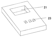
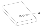
図5は共通液室及び個別液室を形成した基材の模式図、図6は共通液室及び連通孔を形成した基材の模式図、図7は連通孔を形成した基材の模式図、図8はノズルを形成した基材の模式図を表す。図5の21は共通液室であり、絞り25を通って個別液室22に液体が流れ込む。絞り25は、共通液室に液体が逆流しにくい、一方向に流体抵抗のある構造が好ましい。図5及び6の23は図8のノズル24と個別液室22をつなぐ流路の連通孔である。それぞれの板状の基材の厚みは異なっていても良いし、同じであっても良い。このような基材の作製方法は、特に限定されないが、エッチングあるいは打ち抜き加工あるいは射出成形で基材を作成するのが好ましい。好ましいノズルの形状および径は、前述した通りである。エッチングあるいは打ち抜き加工の条件は、基材の厚さ、材料等によって好適な条件を選択する。射出成形の場合は、剛性確保の点で複合材料を用いることが好ましい。
【0038】
本発明の製造方法では、振動板の形成工程が、基板のドライエッチング及びウェットエッチングの少なくとも一つの工程であることが好ましい。エッチング方法を用いることによって、振動板を膜厚の均一な薄膜の状態で残すことができると共に、振動板の可動部の空間を確保することができる。ドライエッチング法を用いる場合、ICP法あるいはFIB法を用いることが好ましい。また、ウェットエッチング法を用いる場合、フッ酸系エッチャントを用いて行うことが好ましい。ドライエッチング及びウェットエッチング工程の条件は、振動板の厚さ、材料等によって好適な条件を選択する。
【0039】
エッチングによる振動板形成工程は、下部電極、圧電・電歪膜、上部電極等が形成された基板を上記形成物がない面からエッチング加工により基板の一部あるいは全部を除去する工程として行なうことができる。エッチングにより除去される部分は、個別液室に対応した部分を含む。振動板の可動部の空間を確保するという観点からは、基板の厚み方向に、個別液室に対応した部分及びその近傍だけを除去する方法でも良い。基板として、SOI基板あるいはSOS基板を用いた場合、SiO2層をエッチングを停止させる層(エッチストップ層)として利用し、残ったSOI層あるいはSOS層を振動板として利用することが好ましい態様である。この場合のSOI基板、SOS基板のハンドルウエハ部の結晶面は(110)であることがウェットエッチングで垂直方向に加工できる点で、好ましい。
【0040】
また、本発明の製造方法における振動板の形成工程には、基板上へ薄膜を形成するための薄膜プロセスも好ましく利用できる。薄膜プロセスとしては、スパッタ法、蒸着法、MBE法、ゾルゲル法(水蒸気加熱も含む)、水熱合成法、CVD法、MO−CVD法、メッキ、電鋳法及びPLD法等を用いることができる。薄膜プロセスの処理条件は振動板の膜厚、材料、使用する方法等によって好適な条件を選択する。薄膜プロセスにより振動板を作成した場合は、振動板部分だけを残すように基板部分は全て加工除去しても良い。
【0041】
また、圧電・電歪膜及び電極上に必要に応じてパッシベーション膜を形成する場合、パッシベーション膜の膜厚は0.1〜10μmが好ましく、より好ましくは、0.2〜5μmである。パッシベーション膜の形成方法としては、スパッタ法、塗布法、CVD法、蒸着等がある。塗布法としては、スクリーン印刷やゾルゲル法などの方式である。形成時に付与する温度は、低温が好ましく、より好ましくは400℃以下、更に好ましくは300℃以下が良い。
【0042】
パッシベーション膜としては、例えば、SiO2、SiN及びSiON等の材料から構成することができる。パッシベーション膜の表面平滑性は、後の接合処理による個別液室形成工程のために平滑であることが望ましいが、個別液室の作製を、接着剤により行う場合には、接着剤の厚みを厚くすることにより補正することが出来る。これは、接着剤の厚みを厚く塗布した後、均一加圧し、接着することにより各素子の表面粗さを補正した接着が出来るためである。又、この場合は、余った接着剤が個別液室、連通孔、ノズル等の部位に入りこまないよう基板内にたまり部を設けることは、有用な手段である。
【0043】
この場合の接着層の厚みは、5μm以上が好ましく、より好ましくは10μm以上である。使用出来る接着剤は、有機系接着剤、有機無機ハイブリッド型接着剤や無機系接着剤であるが、好ましくは、有機無機ハイブリッド型接着剤あるいは無機系接着剤が良い。次に本発明を、実施例を挙げて説明する。
【0044】
【実施例】
(実施例1)
厚み625μmのSOI基板(SOI層およびハンドルウェハ層の結晶面が(110)でSOI層の膜厚が2μm、ボックス層のSiO2膜厚が0.3μm)のSOI層上にSrRuO3(100)の下部電極をスパッタ法により0.2μmで成膜した。この電極上に電歪膜のPMN−PT(組成比PMN66%−PT34%)膜をゾルゲル法により結晶性92%、膜厚3.5μmで成膜した。この電歪膜上に、下部電極と同様に上部電極として、SrRuO3膜をスパッタ法により0.1μmを、メタルマスクを介して成膜した。電歪膜をパターニングしたのち、パッシベーション膜として、ゾルゲル薄膜(加熱温度200℃)のSiO2膜を約0.3μmの厚みで積層した。この上にSUS304で作成した個別液室とノズル部を(ノズル径17μm)有する構造部材を接着剤で貼りあわせた。
【0045】
この構造部材のノズルプレートの厚みは80μm、個別液室部の厚みは150μmである。このノズルプレートと個別液室のSUS基材も、同じ接着剤で貼りあわせたものを用いた。個別液室の幅は55μm、長さは2.5mm、隔壁部の幅は30μmになるように打ち抜き加工したSUS304基材を用いた。個別液室部を接着後、SOI基板のハンドルウェハ部をアルカリエッチング(TMAH溶液)し、個別液室部に相当する部分を除去し、SOI層が振動板となるように薄膜化した。エッチングでは、基板を上面から見た形状が、幅60μm、長さ3.0mmの平行四辺形状にエッチングした。また、個別液室に液体を入れる共通液室を連通させ、共通液室に液体を入れる挿入孔を、SOI基板全体を貫通させて作成した。こうして、本発明のインクジェットヘッドを得た。Si振動板の厚みムラは、個別液室100室を測定したところ、2%以内の±20nmにすべておさまる精度の良いものであった。
【0046】
このヘッドを用いて、周波数10kHz、20Vの駆動電圧を掛けて吐出特性を評価したところ、粘度3cpsの溶液を約11m/秒の速度で効率良く安定して、吐出することが出来た。
【0047】
(実施例2)
下部電極を0.15μm厚のPt,電歪膜をゾルゲル法で形成した2μm厚のPZT圧電膜(Zr/Ti=50/50、結晶性(001)配向性が92%)、上部電極を0.2μm厚の金電極に変え、個別液室の幅を110μm、長さを3mm、隔壁部の幅を60μmにかえて実施例1と同様にヘッドを作成した。実施例2のヘッドはハンドルウェハ部のエッチング除去部を、個別液室5個相当分を除去し、5個の個別液室間ごとに50μm幅の基材を隔壁部に相当する部分上に残して作成した。
実施例1と同様に評価したところ、周波数10kHz、駆動電圧30Vで効率良く液滴の吐出が確認出来た。
【0048】
(実施例3)
実施例1のSOI基板の厚みを625μmから825μm(SOI層およびハンドルウェハ層の結晶面が(110)でSOI層の膜厚が2.5μm、ボックス層の膜厚が0.2μmの基板)に変え、基板のエッチング時間を調節して、幅50μm、長さ2.5mmの平行四辺形状にエッチングして振動板を得た以外は実施例1と同様にインクジェットヘッドを作成し、周波数8kHz、駆動電圧25Vで効率良く液滴の吐出が確認出来た。
【0049】
(比較例1)
厚み625μmのSi基板上に下部電極として、SrTiO3をスパッタ法で成膜し、実施例1と同様に下部電極上にゾルゲル法でPMN−PTの電歪膜を成膜した。さらに、基板の二つの面のうち下部電極及びPMN−PT電歪膜が形成されている面と反対側の面に、実施例1と同様の組成・方法により上部電極を成膜した。ヘッドの個別液室の深さを150μmとするために、基板を研磨により薄膜化した後、ドライプロセスで個別液室を作製した。次に、実施例1で用いたものと同じ仕様のノズルプレートと上記加工済みSi基板を接着剤で接合処理しインクジェットヘッドを得た。
【0050】
このようにして得たヘッドは、基板の研磨むらにより接合不良が発生し、不吐出のノズル部が10%以上存在し、好ましくなかった。また、薄膜化工程で、電歪膜の剥離も発生し、生産効率的に劣るものであった。基板の厚みを、そのまま個別液室の深さとして、ヘッドを作製した場合は、不吐出のノズルは、存在しなかったが、実施例1と比べて、吐出スピードが10〜15%遅くなり、ノズル間の吐出特性も、ばらつきが大きくなった。
【0051】
【発明の効果】
以上、説明したように本発明のユニモルフ型インクジェットヘッドは新規構成で精度良く、かつ安定した液滴吐出が可能であり、また、厚みの異なる基板を用いても精度が良く、特性ばらつきの少ないインクジェットヘッドを得ることが出来る。
本発明は、圧電・電歪膜を形成する基板は一部残す例を説明したが、図2の基板11の全てを除去したインクジェットヘッドあるいはアクチュエータを作成しても良い。
【図面の簡単な説明】
【図1】従来技術によるインクジェットヘッドの模式断面図である。
【図2】本発明のインクジェットヘッドの模式断面図である。
【図3】本発明の連通孔及びノズルの模式断面図である。
【図4】本発明のインクジェットヘッドの他の実施形態の断面図である。
【図5】本発明の共通液室及び個別液室を形成した基材の模式図である。
【図6】本発明の共通液室及び連通孔を形成した基材の模式図である。
【図7】本発明の連通孔を形成した基材の模式図である。
【図8】本発明のノズルを形成した基材の模式図である。
【符号の説明】
1 圧電・電歪膜
2 下部電極
3 振動板
4 個別液室
5 連通孔プレート
6 ノズルプレート
7 ノズル
8 上部電極
9 隔壁
11 基板
12 個別液室プレート
13 連通孔
21 共通液室
22 個別液室
23 連通孔
24 ノズル
25 絞り
30 個別液室を形成する基材
H 個別液室の厚み
W 個別液室の幅
Z 隔壁の幅[0001]
TECHNICAL FIELD OF THE INVENTION
The present invention relates to a unimorph type inkjet head having a novel structure and a manufacturing method for obtaining the inkjet head. More specifically, the present invention relates to an ink jet head which can easily cope with a change in specifications and a method of manufacturing the same.
[0002]
[Prior art]
In recent years, in fields such as optics and precision processing, displacement elements that adjust the optical path length and position on the order of sub-microns and detection elements that detect minute displacements as electrical changes have become desired. Actuators and sensors that respond to displacement caused by the inverse piezoelectric effect or electrostrictive effect that occurs when an electric field is applied to a piezoelectric / electrostrictive material using a ferroelectric substance, or vice versa The development of piezoelectric / electrostrictive elements such as described above is underway.
[0003]
Incidentally, in an ink jet print head or the like, a conventionally known unimorph type is suitably adopted as such a piezoelectric / electrostrictive element structure. There is a demand for improvements in the printing quality and printing speed of printers using such elements, and in order to meet such demands, the piezoelectric / electrostrictive film type elements have been reduced in size and density and driven at lower voltages. Development for achieving high-speed response and long nozzles has been promoted.
[0004]
To overcome these problems, Patent Literature 1 discloses a technique for providing a strong bonding strength by simultaneously sintering a piezoelectric ceramic and a ceramic diaphragm as a piezoelectric speaker. Further, Patent Document 2 discloses a method of manufacturing an ink jet head by forming a piezoelectric film on a silicon substrate by a sol-gel method or a sputtering method. In this method, a silicon substrate is processed to form individual liquid chambers (pressure chambers) to obtain a head.
[0005]
Patent Document 3 discloses an ink jet head including a substrate on which an ink flow path is formed and a nozzle plate having a nozzle, in which a hole diameter of an ink discharge port of the nozzle is formed to be small, and a hole on a side communicating with the flow path. An inkjet head in which the diameter is larger than the diameter of the flow path is described. Patent Document 4 describes a method of manufacturing a piezoelectric film type actuator by using a process of forming a piezoelectric film on a substrate and transferring the film to a lower electrode.
[0006]
[Patent Document 1]
JP-A-62-213399
[Patent Document 2]
U.S. Pat. No. 5,265,315
[Patent Document 3]
JP-A-3-297765
[Patent Document 4]
JP-A-2002-134806
[0007]
[Problems to be solved by the invention]
FIG. 1 is a cross-sectional view of a conventional example of a unimorph type inkjet head. In the figure, 1 is a piezoelectric / electrostrictive film, 2 is a lower electrode, 3 is a vibration plate, 4 is an individual liquid chamber, and 6 is a nozzle plate on which a nozzle 7 is formed. In order to increase the density of the nozzles of the ink jet head, it is necessary to reduce the width of the individual liquid chamber 4 and the width of the partition 9, and even if the widths of the individual liquid chambers 4 become small, a sufficient displacement amount for discharging the droplets is required. It is.
In the unimorph type piezoelectric / electrostrictive element of which density is increased by such a method, it is important to reduce the thickness of the substrate serving as the diaphragm 3 in order to obtain large bending displacement and generated force. However, when the thickness of such a substrate is reduced, there may be a problem that strength is reduced and variation is increased due to the influence of thickness unevenness.
[0008]
According to the method of Patent Document 1, it is possible to join the piezoelectric body and the diaphragm with a strong joining strength. However, this method sinters different materials at a high temperature, so that the diaphragm and the piezoelectric ceramic itself shrink. On the other hand, when producing a large area, it is sometimes difficult to adjust the dimensional accuracy on the order of microns.
[0009]
Further, in the method of Patent Document 2, the thickness of the silicon substrate is equal to the depth of the individual liquid chamber, and it may not be possible to adaptively cope with the required discharge droplet amount and discharge pressure. For example, the thickness of a general-purpose product when the substrate size is 6 inches is 500 to 700 μm, and when the substrate size is 8 inches, it is 600 to 800 μm. When an individual liquid chamber is formed by using these substrates, the thickness of the substrate becomes the depth of the individual liquid chamber, which is not preferable in terms of head specifications such as setting of the amount of discharged droplets. In addition, when the substrate is thinned by polishing or the like to cope with the problem, there is a case where a problem that the length of the head cannot be accommodated due to uneven thickness due to polishing or the like occurs. In the ink jet head described in Patent Document 3, air bubbles may accumulate between the nozzle plate and the communication hole substrate.
[0010]
An object of the present invention is to provide a unimorph type actuator and an inkjet head which solve the above problems. Another object of the present invention is to provide an actuator and an ink jet head having high reliability with multiple nozzles. That is, an object of the present invention is to provide an actuator / ink jet head which can provide a large displacement with a low driving voltage, has a high response speed, has a large generating force, and is capable of multi-nozzle and high integration. Another object of the present invention is to provide an ink jet head which has a high rigidity of the partition wall, can make the depth of the individual liquid chamber as small as 200 μm or less, and has an excellent droplet discharge speed.
[0011]
[Means for Solving the Problems]
In a unimorph type inkjet head having an individual liquid chamber communicating with a discharge port, a diaphragm and a piezoelectric / electrostrictive element, a part of the inner wall of the individual liquid chamber is formed as a vibrating portion having a diaphragm. The piezoelectric / electrostrictive element is arranged on the vibrating part on the side of the individual liquid chamber. That is, the inkjet head of the present invention has a configuration in which the diaphragm is located below the piezoelectric / electrostrictive element and at least a part of the individual liquid chamber is located above the piezoelectric / electrostrictive element. Here, the positional relationship between the individual liquid chamber, the piezoelectric / electrostrictive element, and the diaphragm is based on the direction in which the nozzle side is up and the substrate side is down with reference to the ink ejection direction. Having the “diaphragm below the piezoelectric / electrostrictive element” means that the uppermost surface of the diaphragm is below the lowermost surface of the piezoelectric / electrostrictive element. Also, "at least a part of the individual liquid chamber is located above the piezoelectric / electrostrictive element" means that the uppermost surface of the individual liquid chamber is above the lowermost surface of the piezoelectric / electrostrictive element. Represents
[0012]
According to the present invention, by placing the piezoelectric / electrostrictive element in the individual liquid chamber side, pressure generation in the piezoelectric / electrostrictive element is affected by the thickness of the diaphragm and the substrate supporting the piezoelectric / electrostrictive element. In addition, it is easy to reduce the width of the individual liquid chamber and the piezoelectric / electrostrictive element, and the dimensional accuracy of the individual liquid chamber is high, the characteristic variation is small, and an inkjet head having a structure suitable for high density nozzles is provided. Can be obtained.
[0013]
BEST MODE FOR CARRYING OUT THE INVENTION
The main part of the ink jet head of the present invention is shown in a schematic perspective view (FIGS. 2 and 4) in which four side surfaces are represented in cross section. That is, FIGS. 2 and 4 show the front side, the back side, and both right and left sides of the head as cross sections, and are perspective views in a state where a nozzle having a discharge port faces downward. In these figures, reference numeral 11 denotes a substrate, which is partially etched up to the diaphragm 3. The portion 11 left by the processing of the substrate corresponds to one individual liquid chamber in the configuration of FIG. 2, but corresponds to one individual liquid chamber in the configuration of FIG. The diaphragm 3 and the lower electrode 2 are formed on 11. The diaphragm 3 may be formed as a part of the substrate, or may be a film newly formed on the substrate or a film bonded thereto. The portion where the laminated body of the diaphragm 3 and the lower electrode 2 forms the inner wall of the individual liquid chamber 4 is a vibrating portion based on the diaphragm, and the piezoelectric / electrostrictive film 1 is disposed on the vibrating portion. ing. An upper electrode (not shown) is provided on the upper surface of the piezoelectric / electrostrictive film 1, and the piezoelectric / electrostrictive film 1 is sandwiched between a region of the lower electrode below the piezoelectric / electrostrictive film 1 and this upper electrode. The piezoelectric / electrostrictive element having the configuration is configured.
[0014]
In this ink jet head, a nozzle having a discharge port extends at a lower end having a central axis in a direction perpendicular to a plane direction of the diaphragm, and an opening surface of the discharge port and a surface of the diaphragm are positioned in parallel. ing. With this configuration, the liquid is discharged from the discharge port located at the lower end of the nozzle perpendicular to the longitudinal direction of the individual liquid chamber in the direction perpendicular to the surface direction of the diaphragm. The direction of discharging the liquid is shown in the figure.
[0015]
According to the present invention, by placing the piezoelectric / electrostrictive element in the individual liquid chamber side, pressure generation in the piezoelectric / electrostrictive element is affected by the thickness of the diaphragm and the substrate supporting the piezoelectric / electrostrictive element. In addition, it is easy to reduce the width of the individual liquid chamber and the piezoelectric / electrostrictive element, and the dimensional accuracy of the individual liquid chamber is high, the characteristic variation is small, and an inkjet head having a structure suitable for high density nozzles is provided. Can be obtained.
[0016]
The depth of the individual liquid chamber 4 can be adjusted by the thickness of the individual liquid chamber plate 12. It is preferable that the piezoelectric / electrostrictive film 1 of the ink jet head of the present invention has a piezoelectric / electrostrictive film sandwiched between a pair of lower electrode 2 and upper electrode (not shown). As shown in the drawing, a piezoelectric / electrostrictive film is provided on a predetermined portion of the surface composed of the lower electrode 2, and an upper electrode is further provided on the piezoelectric / electrostrictive film. For example, the upper electrode is selected (driven) by using the lower electrode as a common electrode. By using it as an electrode, image digital information can be transmitted to the piezoelectric / electrostrictive film with high accuracy.
[0017]
Portions of the upper electrode and the lower electrode that are in contact with the individual liquid chambers are made of a material having resistance to a liquid. For example, by forming a passivation film on a surface of the electrode which is in contact with the liquid, resistance to the liquid can be imparted to the electrode.
The inkjet head having the above configuration is, for example, a method for manufacturing a unimorph inkjet head having an individual liquid chamber communicating with the discharge port, a diaphragm, and a piezoelectric / electrostrictive element.
A step of forming a lower electrode on a portion of the substrate to be a diaphragm,
Forming a piezoelectric / electrostrictive film on the lower electrode;
Forming an upper electrode on the piezoelectric / electrostrictive film to form a piezoelectric / electrostrictive element;
Forming a separate liquid chamber containing at least a part of the piezoelectric / electrostrictive element,
Communicating with the individual liquid chamber, forming a nozzle having a discharge port,
Can be manufactured by a method for manufacturing an ink jet head characterized by having:
[0018]
In particular, the substrate of the present invention is preferably a silicon substrate, an SOI substrate (silicon on insulator) or an SOS substrate (silicon on sapphire). By using these substrates, it is possible to obtain a diaphragm having large displacement at low driving voltage, high mechanical strength, and excellent film thickness uniformity. The method for forming a diaphragm of the present invention is preferably based on at least one of dry etching and wet etching of the substrate. Further, the method for forming the diaphragm of the present invention is preferably a method using a thin film process.
[0019]
Each component of the ink jet head of the present invention will be described in more detail.
The thickness (thickness in the ink ejection direction) of the piezoelectric / electrostrictive film is preferably 1 μm or more and 30 μm or less, more preferably 1 μm or more and 10 μm or less. The thickness of the diaphragm is preferably 1 μm or more and 30 μm or less, more preferably 1 μm or more and 10 μm or less. The width of the individual liquid chamber (W in FIGS. 2 and 4, the distance between the individual liquid chamber plates) can be set arbitrarily, but is preferably 30 μm or more and 500 μm or less, more preferably 30 μm or more and 150 μm or less.
[0020]
The length of the individual liquid chamber (L in FIGS. 2 and 4, the distance between the inner wall surface of the individual liquid chamber (the plane parallel to the central axis of the nozzle) in the direction perpendicular to the central axis of the nozzle) is arbitrary. Can be set to 50 μm or more and 6000 μm or less, more preferably 300 μm or more and 3000 μm or less. The depth of the individual liquid chamber (H in FIGS. 2 and 4, the length in the ink ejection direction) can be set arbitrarily, but is preferably 30 μm or more and 400 μm or less, more preferably 50 μm or more and 200 μm or less. The nozzle may have a cross section perpendicular to the central axis, such as a circle, a star, a triangle, or a quadrangle. Preferably, the cross section is a circle or a star. When the cross section is circular, the nozzle diameter is preferably 5 μm or more and 50 μm or less, and more preferably 7 μm or more and 30 μm or less.
[0021]
It is preferable that a communication hole 13 connecting the individual liquid chamber and the nozzle is provided. The schematic diagram of FIG. 2 is an example in which two communication holes are formed on the nozzle plate 6 using two plate members. However, the communication holes may not be provided. FIG. 2 shows an example in which a plate member provided with an individual liquid chamber and a substrate provided with a diaphragm and the like are further provided. The diameter of the communication hole 13 is larger than the nozzle diameter. The nozzle preferably has a tapered shape between the nozzle plates. When the nozzle diameter is 10 to 30 μm, the hole diameter on the communication hole side is preferably 15 to 60 μm.
[0022]
The thickness of the nozzle plate 6 is preferably 30 μm or more and 150 μm or less. The length of the communication hole in the ink discharge direction is preferably 30 μm or more and 300 μm or less. The nozzle plate 6 may have a structure in which the nozzle 7 and the communication hole 13 are formed in one base material as shown in the sectional view of FIG.
[0023]
As a method of forming the communication hole portion and the nozzle portion, a method of joining the base material on which each hole is formed, or a method of forming each portion by a method such as electroforming, plating, vapor deposition, or injection molding can be employed. Examples of the base material for forming the holes include a silicon base material, a SUS base material, a Ni base material, a polymer material, a carbon material, and a composite material containing carbon and silica. In the case of a method such as electroforming, plating, or vapor deposition, the film is formed such that a portion for forming a hole or a concave portion is formed by patterning using a resist or a mask. The preferred Young's modulus of the plate material forming the nozzle portion and the communication hole portion is 0.1 GPa or more. When the pressure is 0.1 GPa or more, the partition does not displace with respect to the displacement of the actuator in the configuration including the diaphragm / piezoelectric / electrostrictive element even when the partition becomes thin, and the ejection performance does not decrease.
[0024]
The piezoelectric / electrostrictive film referred to in the present invention means a piezoelectric film and / or an electrostrictive film. As a material used for the piezoelectric / electrostrictive film, a perovskite-type compound may be used. For example, lead zirconate titanate PZT [Pb (Zr x Ti 1-x ) O 3 ] And barium titanate BaTiO 3 Such as a piezoelectric material and a relaxor-based electrostrictive material. The x of lead zirconate titanate (PZT) is preferably an MPB (morphotropic phase boundary) composition of 0.40 to 0.65, but other composition ratios may be used. The crystal structure of PZT may be any of tetragonal and rhombohedral. BaTiO 3 Is preferably a tetragonal (001) -oriented film. In addition, BaTiO 3 May contain trace amounts of lead and bismuth.
[0025]
The following can be selected as the electrostrictive material used in the present invention. For example, PMN [Pb (Mg x Nb 1-x ) O 3 ], PNN [Pb (Nb x Ni 1-x ) O 3 ], PSN [Pb (Sc x Nb 1-x ) O 3 ], PZN [Pb (Zn x Nb 1-x ) O 3 ], PMN-PT {(1-y) [Pb (Mg x Nb 1-x ) O 3 ] -Y [PbTiO 3 ]}, PSN-PT {(1-y) [Pb (Sc x Nb 1-x ) O 3 ] -Y [PbTiO 3 ]}, PZN-PT {(1-y) [Pb (Zn x Nb 1-x ) O 3 ] -Y [PbTiO 3 ]}, LN [LiNbO 3 ], KN [KNbO 3 ].
[0026]
Here, x and y are numbers of 1 or less and 0 or more. For example, x is 0.2 to 0.5 for PMN, 0.2 to 0.5 for PNN, x is 0.4 to 0.7 for PSN, and x is 0.1 to 0 for PZN. 0.5, y of PMN-PT is preferably 0.2 to 0.4, y of PSN-PT is 0.35 to 0.5, and y of PZN-PT is preferably 0.03 to 0.35. Also, PMN-PZT, PZN-PZT, PNN-PZT, and PSN-PZT compounds in which Zr is substituted for part of Ti in PMN-PT, PZN-PT, PNN-PT, and PSN-PT. Is also good.
[0027]
The piezoelectric / electrostrictive film may have a single composition or a combination of two or more types. Further, a composition in which the above main component is doped with a trace element may be used. In order for the piezoelectric / electrostrictive film of the present invention to exhibit excellent piezoelectricity, it is preferable that the piezoelectric / electrostrictive film is crystal-controlled, and that a specific orientation of a specific crystal structure is 50% or more by X-ray diffraction. Certain ones are preferred, and those with 90% or more are more preferred. The crystal grain size of the piezoelectric / electrostrictive film is preferably 0.02 μm or more. The crystal grain size may be granular or island-like flowing in the film thickness direction. In a single crystal film, the size of the crystal grain size may not be visually recognized in some cases.
[0028]
As the electrode material, a metal or a conductive metal oxide is used. Examples of the metal include Pt, Au, Ni, Ir, Os, Cr, and SUS. The conductive metal oxide is preferably a perovskite compound, for example, SrRuO 3, La-doped-SrTiO 3 , La-doped-SrCoO 3 , Nb-doped-SrTiO 3 , BaPbO 3 , LaNiO 3 , LaCrO 3 , CaRuO 3 And so on. The material of the upper electrode and the material of the lower electrode may be different materials or the same material. Further, an anchor layer may be provided below the electrode for improving adhesiveness. As the anchor layer, for example, a metal material such as Ti, Cr, Pb, Ir or TiO 2 And metal oxides such as IrO. The thickness of the electrode is preferably from 0.05 to 1.0 μm, more preferably from 0.1 to 0.3 μm.
[0029]
The material of the diaphragm varies depending on the manufacturing method selected as described later, 2 , YSZ, PSZ, ZrO 2 Or the electrode may also serve as the diaphragm. When the electrode also serves as the vibration plate, the thickness of the electrode is preferably not in the above range but 0.5 μm to 6 μm. The preferred Young's modulus of the diaphragm is 10 to 300 GPa. For example, when the Si substrate is used as the diaphragm, the pressure is 100 to 160 GPa.
[0030]
Next, the method for manufacturing an ink jet head of the present invention having the above-mentioned steps will be further described. In the ink jet head of the present invention, the thickness of the diaphragm and / or the piezoelectric / electrostrictive film is preferably 1 μm or more and 30 μm or less, more preferably 1 μm or more and 10 μm or less. For this reason, the total thickness of the obtained inkjet head is about several hundred μm to 1 mm, and when a large-area head is created, this is a manufacturing method that eliminates the inconvenience in the manufacturing process in which an ultra-thin substrate must be used. This is a manufacturing method in which the actuator section becomes a thin film regardless of the thickness of the substrate.
[0031]
Furthermore, the manufacturing method of the present invention may further include a step of patterning the upper electrode and / or the piezoelectric / electrostrictive film in addition to the above steps. Further, the manufacturing method of the present invention is a manufacturing method preferably including a step of forming a passivation film on the piezoelectric / electrostrictive film.
[0032]
The steps of the present invention will be described sequentially in more detail. The lower electrode forming step is a method of forming one electrode for applying an electric field to the piezoelectric / electrostrictive film. The lower electrode is formed by sputtering, sol-gel, printing, vapor deposition, plating, electroforming, MO-CVD, The electrodes can be formed by a method such as a PLD method. Suitable conditions for manufacturing the lower electrode are selected according to the thickness, material, method used, and the like of the lower electrode. The electrode material is as described above, and the electrode layer may be crystal-controlled. For example, a metal material is a film oriented or single-crystallized to (111) or (100), and an oxide electrode is similarly oriented or single-crystallized to (100), (111) or (110). That is the preferred embodiment.
[0033]
The steps of forming a piezoelectric / electrostrictive film include sputtering, vapor deposition, MBE, sol-gel (including steam heating), hydrothermal synthesis, CVD, MO-CVD, gas deposition, PLD, etc. In the thin film process. As another method, a method of joining and bonding piezoelectric / electrostrictive films formed by a sintering method or a molten single crystal method may be used. Further, as described in Patent Literature 4, a piezoelectric / electrostrictive film may be formed on a base material and then transferred to a lower electrode. Suitable conditions for producing the piezoelectric / electrostrictive film are selected according to the thickness, material, method used and the like of the piezoelectric / electrostrictive film.
[0034]
The step of forming the upper electrode can be similar to that of the lower electrode. The electrodes are formed as selection electrodes in which either the upper electrode or the lower electrode is independently connected to each piezoelectric / electrostrictive film in order to individually drive the actuators. As described above, in the manufacturing process, it is preferable to pattern the upper electrode as a selection electrode. Since the step of forming the upper electrode is a step after the piezoelectric / electrostrictive film is formed, it is not preferable to form the upper electrode at a temperature exceeding the Curie temperature of the piezoelectric / electrostrictive film. More preferably, the film is formed at 300 ° C. or lower.
[0035]
Other conditions for manufacturing the upper electrode are appropriately selected depending on the thickness, material, method used, and the like of the upper electrode. The upper electrode and the piezoelectric / electrostrictive film are patterned by at least one of dry etching and wet etching. It is preferable to use the ICP method or the FIB method as the dry etching. It is preferable that the wet etching be performed using a hydrofluoric acid-based etchant. The wet etching step may be performed under heating. Suitable conditions for the dry etching and the wet etching are selected according to the thickness, material, method to be used, and the like of the upper electrode and the piezoelectric / electrostrictive film.
[0036]
The formation of the individual liquid chamber is preferably performed after the step of patterning the piezoelectric / electrostrictive film and the upper electrode. The individual liquid chamber forming step is a step of separately joining and bonding a concave portion serving as an individual liquid chamber and a member having a nozzle portion corresponding to the concave portion. As another method, a mold for the concave portion and the nozzle portion is formed on a piezoelectric / electrostrictive film using a resist material, and a wall material is formed on a portion other than the portion covered with the mold by a plating method, an electroforming method, or the like. It may be formed by forming a film. A preferred step is the former method. As a method of forming the former member, for example, using one or a plurality of metal plates such as SUS or a silicon base material, a nozzle portion, a communication hole portion, and an individual liquid chamber are formed, and these are laminated. A method of forming a member can be given.
[0037]
FIG. 5 is a schematic view of a base material having a common liquid chamber and an individual liquid chamber, FIG. 6 is a schematic view of a base material having a common liquid chamber and a communication hole, and FIG. 7 is a schematic view of a base material having a communication hole. FIG. 8 is a schematic view of a substrate on which a nozzle is formed. 5 is a common liquid chamber, and the liquid flows into the individual liquid chamber 22 through the throttle 25. The restrictor 25 preferably has a structure in which liquid does not easily flow back into the common liquid chamber and has fluid resistance in one direction. Reference numeral 23 in FIGS. 5 and 6 denotes a communication hole of a flow path connecting the nozzle 24 and the individual liquid chamber 22 in FIG. The thickness of each plate-shaped substrate may be different or the same. The method for producing such a substrate is not particularly limited, but it is preferable to produce the substrate by etching, punching, or injection molding. Preferred nozzle shapes and diameters are as described above. Suitable conditions for etching or punching are selected depending on the thickness, material, and the like of the base material. In the case of injection molding, it is preferable to use a composite material from the viewpoint of securing rigidity.
[0038]
In the manufacturing method of the present invention, it is preferable that the step of forming the diaphragm is at least one of dry etching and wet etching of the substrate. By using the etching method, the diaphragm can be left in a state of a thin film having a uniform thickness, and a space for a movable portion of the diaphragm can be secured. When a dry etching method is used, it is preferable to use an ICP method or a FIB method. When a wet etching method is used, it is preferable to use a hydrofluoric acid-based etchant. Suitable conditions for the dry etching and wet etching steps are selected according to the thickness and material of the diaphragm.
[0039]
The vibration plate forming step by etching may be performed as a step of removing a part or the whole of the substrate on which the lower electrode, the piezoelectric / electrostrictive film, the upper electrode, and the like are formed by etching from the surface where the above-mentioned formation is not formed. it can. The portion removed by etching includes a portion corresponding to the individual liquid chamber. From the viewpoint of securing a space for the movable portion of the diaphragm, a method of removing only a portion corresponding to the individual liquid chamber and its vicinity in the thickness direction of the substrate may be used. When an SOI substrate or SOS substrate is used as the substrate, SiO 2 In a preferred embodiment, the layer is used as a layer for stopping etching (etch stop layer), and the remaining SOI layer or SOS layer is used as a diaphragm. In this case, the crystal plane of the handle wafer portion of the SOI substrate or the SOS substrate is preferably (110) in that it can be processed in a vertical direction by wet etching.
[0040]
In the step of forming a diaphragm in the manufacturing method of the present invention, a thin film process for forming a thin film on a substrate can also be preferably used. As the thin film process, a sputtering method, an evaporation method, an MBE method, a sol-gel method (including steam heating), a hydrothermal synthesis method, a CVD method, an MO-CVD method, a plating method, an electroforming method, a PLD method, and the like can be used. . Suitable processing conditions for the thin film process are selected according to the film thickness of the diaphragm, the material, the method used, and the like. When a diaphragm is formed by a thin film process, the entire substrate portion may be processed and removed so as to leave only the diaphragm portion.
[0041]
When a passivation film is formed on the piezoelectric / electrostrictive film and the electrode as required, the thickness of the passivation film is preferably from 0.1 to 10 μm, more preferably from 0.2 to 5 μm. As a method for forming the passivation film, there are a sputtering method, a coating method, a CVD method, an evaporation method, and the like. The coating method is a method such as screen printing or a sol-gel method. The temperature applied during the formation is preferably low, more preferably 400 ° C. or lower, and further preferably 300 ° C. or lower.
[0042]
As the passivation film, for example, SiO 2 2 , SiN and SiON. It is desirable that the surface smoothness of the passivation film be smooth for the individual liquid chamber forming step by the subsequent bonding process. However, when the individual liquid chamber is manufactured using an adhesive, the thickness of the adhesive is increased. Can be corrected. This is because, after a thick adhesive is applied, uniform pressure is applied and bonding is performed so that bonding with corrected surface roughness of each element can be performed. In this case, it is a useful means to provide a pool in the substrate so that the surplus adhesive does not enter the individual liquid chambers, communication holes, nozzles and the like.
[0043]
In this case, the thickness of the adhesive layer is preferably 5 μm or more, more preferably 10 μm or more. Adhesives that can be used are organic adhesives, organic-inorganic hybrid adhesives and inorganic adhesives, and preferably organic-inorganic hybrid adhesives or inorganic adhesives. Next, the present invention will be described with reference to examples.
[0044]
【Example】
(Example 1)
SOI substrate having a thickness of 625 μm (the crystal plane of the SOI layer and the handle wafer layer is (110), the thickness of the SOI layer is 2 μm, and the SiO 2 SrRuO on the SOI layer having a thickness of 0.3 μm) 3 The lower electrode of (100) was formed to a thickness of 0.2 μm by sputtering. An electrostrictive PMN-PT film (composition ratio: 66% -34% PTN) was formed on this electrode by a sol-gel method with a crystallinity of 92% and a thickness of 3.5 μm. On this electrostrictive film, SrRuO 3 The film was formed to a thickness of 0.1 μm by a sputtering method via a metal mask. After patterning the electrostrictive film, a sol-gel thin film (heating temperature: 200 ° C.) of SiO is used as a passivation film. 2 The film was laminated at a thickness of about 0.3 μm. On top of this, an individual liquid chamber made of SUS304 and a structural member having a nozzle portion (nozzle diameter 17 μm) were bonded with an adhesive.
[0045]
The thickness of the nozzle plate of this structural member is 80 μm, and the thickness of the individual liquid chamber is 150 μm. The nozzle plate and the SUS substrate of the individual liquid chamber were also used with the same adhesive. An SUS304 base material punched out so that the width of the individual liquid chamber was 55 μm, the length was 2.5 mm, and the width of the partition wall was 30 μm was used. After bonding the individual liquid chambers, the handle wafer part of the SOI substrate was subjected to alkali etching (TMAH solution) to remove a portion corresponding to the individual liquid chambers, and the SOI layer was thinned so as to be a diaphragm. In the etching, the shape of the substrate viewed from above was etched into a parallelogram having a width of 60 μm and a length of 3.0 mm. In addition, the common liquid chamber for putting the liquid into the individual liquid chambers was communicated, and the insertion hole for putting the liquid into the common liquid chamber was formed by penetrating the entire SOI substrate. Thus, the inkjet head of the present invention was obtained. The thickness unevenness of the Si diaphragm was measured with accuracy in 100 individual liquid chambers, and was found to be highly accurate within 2% within ± 20 nm.
[0046]
Using this head, a discharge voltage was evaluated by applying a drive voltage of 10 kHz and a voltage of 20 V. As a result, a solution having a viscosity of 3 cps could be discharged efficiently and stably at a speed of about 11 m / sec.
[0047]
(Example 2)
The lower electrode is 0.15 μm thick Pt, the 2 μm thick PZT piezoelectric film (Zr / Ti = 50/50, crystallinity (001) orientation is 92%), and the upper electrode is 0 μm. A head was prepared in the same manner as in Example 1 except that the width of the individual liquid chamber was changed to 110 μm, the length was changed to 3 mm, and the width of the partition was changed to 60 μm. In the head of Example 2, the etching removal portion of the handle wafer portion was removed for five individual liquid chambers, and a base material having a width of 50 μm was left between the five individual liquid chambers on the portion corresponding to the partition wall. Created.
Evaluation was performed in the same manner as in Example 1. As a result, discharge of droplets was efficiently confirmed at a frequency of 10 kHz and a driving voltage of 30 V.
[0048]
(Example 3)
The thickness of the SOI substrate of Example 1 was changed from 625 μm to 825 μm (a substrate in which the crystal plane of the SOI layer and the handle wafer layer is (110), the thickness of the SOI layer is 2.5 μm, and the thickness of the box layer is 0.2 μm). The inkjet head was prepared in the same manner as in Example 1 except that the vibration time was obtained by changing the etching time of the substrate and etching into a parallelogram having a width of 50 μm and a length of 2.5 mm, and driving at a frequency of 8 kHz. Efficient discharge of droplets was confirmed at a voltage of 25 V.
[0049]
(Comparative Example 1)
SrTiO was used as a lower electrode on a 625 μm thick Si substrate. 3 Was formed by a sputtering method, and an electrostrictive film of PMN-PT was formed on the lower electrode by a sol-gel method as in Example 1. Further, an upper electrode was formed on the opposite surface of the two surfaces of the substrate from the surface on which the lower electrode and the PMN-PT electrostrictive film were formed by the same composition and method as in Example 1. In order to make the depth of the individual liquid chamber of the head 150 μm, the substrate was thinned by polishing, and then the individual liquid chamber was formed by a dry process. Next, a nozzle plate having the same specifications as those used in Example 1 and the processed Si substrate were joined with an adhesive to obtain an ink jet head.
[0050]
The thus obtained head was unfavorable because bonding defects occurred due to uneven polishing of the substrate, and non-ejection nozzles were present in 10% or more. Further, in the thinning process, the electrostrictive film was peeled off, which was inferior in production efficiency. When the head was manufactured with the thickness of the substrate being the depth of the individual liquid chamber as it was, there was no non-discharge nozzle, but the discharge speed was 10 to 15% slower than in Example 1. The discharge characteristics between the nozzles also showed large variations.
[0051]
【The invention's effect】
As described above, the unimorph type ink jet head of the present invention has a novel structure and is capable of discharging liquid droplets with high accuracy and stability, and has good accuracy even with substrates having different thicknesses and has a small characteristic variation. You can get a head.
Although the present invention has been described with respect to an example in which the substrate on which the piezoelectric / electrostrictive film is formed is partially left, an ink jet head or actuator in which the entire substrate 11 in FIG.
[Brief description of the drawings]
FIG. 1 is a schematic sectional view of an ink jet head according to the related art.
FIG. 2 is a schematic sectional view of the inkjet head of the present invention.
FIG. 3 is a schematic sectional view of a communication hole and a nozzle of the present invention.
FIG. 4 is a sectional view of another embodiment of the ink jet head of the present invention.
FIG. 5 is a schematic view of a substrate on which a common liquid chamber and individual liquid chambers of the present invention are formed.
FIG. 6 is a schematic view of a base material having a common liquid chamber and a communication hole according to the present invention.
FIG. 7 is a schematic view of a base material having a communication hole according to the present invention.
FIG. 8 is a schematic view of a substrate on which a nozzle of the present invention is formed.
[Explanation of symbols]
1 Piezoelectric and electrostrictive films
2 Lower electrode
3 diaphragm
4 Individual liquid chamber
5 Communication hole plate
6 Nozzle plate
7 nozzle
8 Upper electrode
9 Partition wall
11 Substrate
12 Individual liquid chamber plate
13 communication hole
21 Common liquid chamber
22 Individual liquid chamber
23 communication hole
24 nozzles
25 Aperture
30 Substrates forming individual liquid chambers
H Thickness of individual liquid chamber
W Width of individual liquid chamber
Z Partition wall width