JP2004227584A - Temperature-compensated bandgap voltage reference circuit - Google Patents
Temperature-compensated bandgap voltage reference circuit Download PDFInfo
- Publication number
- JP2004227584A JP2004227584A JP2004011119A JP2004011119A JP2004227584A JP 2004227584 A JP2004227584 A JP 2004227584A JP 2004011119 A JP2004011119 A JP 2004011119A JP 2004011119 A JP2004011119 A JP 2004011119A JP 2004227584 A JP2004227584 A JP 2004227584A
- Authority
- JP
- Japan
- Prior art keywords
- vbe
- δvbe
- voltage
- comparator
- circuit
- Prior art date
- Legal status (The legal status is an assumption and is not a legal conclusion. Google has not performed a legal analysis and makes no representation as to the accuracy of the status listed.)
- Pending
Links
Images


Classifications
-
- G—PHYSICS
- G05—CONTROLLING; REGULATING
- G05F—SYSTEMS FOR REGULATING ELECTRIC OR MAGNETIC VARIABLES
- G05F3/00—Non-retroactive systems for regulating electric variables by using an uncontrolled element, or an uncontrolled combination of elements, such element or such combination having self-regulating properties
- G05F3/02—Regulating voltage or current
- G05F3/08—Regulating voltage or current wherein the variable is dc
- G05F3/10—Regulating voltage or current wherein the variable is dc using uncontrolled devices with non-linear characteristics
- G05F3/16—Regulating voltage or current wherein the variable is dc using uncontrolled devices with non-linear characteristics being semiconductor devices
- G05F3/20—Regulating voltage or current wherein the variable is dc using uncontrolled devices with non-linear characteristics being semiconductor devices using diode- transistor combinations
- G05F3/30—Regulators using the difference between the base-emitter voltages of two bipolar transistors operating at different current densities
Abstract
Description
本発明は、温度補償されたバンドギャップ電圧基準に関する。 The present invention relates to a temperature compensated bandgap voltage reference.
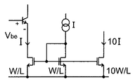
図1に、バイポーラトランジスタのVbeに基づいて基準電圧を得る方法を示す。電流源Iは、バイポーラトランジスタのエミッタパスに提供されている。複数の電流源は、サイズの異なるFETが各々接続され、異なる値の電流、例えばI、10Iを供給する。 FIG. 1 shows a method for obtaining a reference voltage based on Vbe of a bipolar transistor. A current source I is provided on the emitter path of the bipolar transistor. The plurality of current sources are connected to FETs having different sizes, respectively, and supply currents having different values, for example, I and 10I.
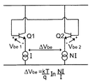
バイポーラトランジスタのVbeは、図3に示すように、既知のとおり、温度が上昇するにつれて減少する。カレントミラーを用いて、ΔVbe、すなわち2つのバイポーラトランジスタのVbeの差分に比例した電圧を得ることが知られている。図2にカレントミラーを示す。ΔVbeは、Vbe2−Vbe1に等しく、ΔVbeは、
kt/qlnNI/I
に等しい。ΔVbeは、温度と同様に電流源の電流比に依存する。特に、ΔVbeは、図3に示すように、温度により増大する。2つの回路を組み合わせることにより、VbeをΔVbeで補償することができ、図3に示した実質的に一定の基準電圧Vrefを得ることができる。特に、Vrefは、
A×Vbe+B×ΔVbe
に等しい。
As is known, the Vbe of a bipolar transistor decreases with increasing temperature, as shown in FIG. It is known to use a current mirror to obtain a voltage proportional to ΔVbe, that is, the difference between Vbe of two bipolar transistors. FIG. 2 shows a current mirror. ΔVbe is equal to Vbe2−Vbe1, and ΔVbe is
kt / qlnNI / I
be equivalent to. ΔVbe depends on the current ratio of the current source as well as the temperature. In particular, ΔVbe increases with temperature, as shown in FIG. By combining the two circuits, Vbe can be compensated for by ΔVbe, and a substantially constant reference voltage Vref shown in FIG. 3 can be obtained. In particular, Vref is
A × Vbe + B × ΔVbe
be equivalent to.
本発明は、VbeとΔVbeとを加算して、実質的に温度に依存しない一定の基準電圧を得ることができるVbeバンドギャップ電圧基準を提供する。回路は、Vbeを与えるバイポーラトランジスタと、ΔVbeのカレントミラーを使用する。コンパレータは、差動増幅器として実装され、VbeとΔVbeに比例した入力を受ける。コンパレータの出力は、Vbeを与えるバイポーラトランジスタの入力に接続される。 The present invention provides a Vbe bandgap voltage reference that can add Vbe and ΔVbe to obtain a constant reference voltage that is substantially independent of temperature. The circuit uses a bipolar transistor that provides Vbe and a current mirror of ΔVbe. The comparator is implemented as a differential amplifier and receives inputs proportional to Vbe and ΔVbe. The output of the comparator is connected to the input of a bipolar transistor providing Vbe.
一態様では、本発明にかかるバンドギャップ電圧基準回路は、第1のバイポーラトランジスタのVbeに実質的に比例する第1の電圧を供給する第1の回路と、2つのバイポーラトランジスタの2つのVbe電圧の差分に実質的に比例する第2の電圧ΔVbeを供給する第2の回路と、VbeとΔVbeに接続された各々の入力および前記第1のバイポーラトランジスタのベースに接続された出力を有するコンパレータとを備え、これにより、VbeとΔVbeとに定数を乗算し、各々の合計に実質的に比例する電圧を、前記コンパレータの出力から供給する。 In one aspect, a bandgap voltage reference circuit according to the present invention comprises: a first circuit for providing a first voltage substantially proportional to Vbe of a first bipolar transistor; and a two Vbe voltage for two bipolar transistors. A second circuit for providing a second voltage ΔVbe substantially proportional to the difference between the first and second bipolar transistors, and a comparator having respective inputs connected to Vbe and ΔVbe and an output connected to the base of the first bipolar transistor. Whereby Vbe and ΔVbe are multiplied by a constant, and a voltage substantially proportional to the sum of each is provided from the output of the comparator.
他の態様では、本発明にかかるバンドギャップ電圧基準回路は、実質的に基準電圧Vbeを供給する第1のバイポーラトランジスタと、2つのバイポーラトランジスタの各々のVbe電圧間の差分信号を実質的に含む差分電圧ΔVbeを供給するカレントミラーを構成するように接続された前記2つのバイポーラトランジスタを含むカレントミラー回路と、VbeとΔVbeに接続された各々の入力および前記第1のバイポーラトランジスタのベースに接続された出力を有するコンパレータとを備え、これにより、VbeとΔVbeとに定数を乗算し、各々の合計に実質的に比例する電圧を、前記コンパレータの出力から供給する。 In another aspect, a bandgap voltage reference circuit according to the present invention substantially includes a first bipolar transistor that provides a substantially reference voltage Vbe and a difference signal between the Vbe voltages of each of the two bipolar transistors. A current mirror circuit including the two bipolar transistors connected to form a current mirror for supplying a differential voltage ΔVbe; a respective input connected to Vbe and ΔVbe; and a base connected to the base of the first bipolar transistor. A comparator having a constant output, whereby Vbe and ΔVbe are multiplied by a constant, and a voltage substantially proportional to the sum of each is provided from the output of the comparator.
さらに他の態様では、本発明にかかるバンドギャップ電圧基準回路は、第1のバイポーラトランジスタのVbeに実質的に比例する第1の電圧を供給する第1の回路と、2つのバイポーラトランジスタの2つのVbe電圧の差分に実質的に比例する第2の電圧ΔVbeを供給する第2の回路と、VbeとΔVbeに接続された各々の入力および前記第1のバイポーラトランジスタのベースに接続された出力を有するコンパレータとを備え、これにより、実質的に温度に依存しない電圧基準を、前記コンパレータの出力から供給する。 In yet another aspect, a bandgap voltage reference circuit according to the present invention includes a first circuit for providing a first voltage substantially proportional to Vbe of a first bipolar transistor, and a two circuit of two bipolar transistors. A second circuit for providing a second voltage .DELTA.Vbe substantially proportional to the difference of the Vbe voltage, having a respective input connected to Vbe and .DELTA.Vbe and an output connected to the base of the first bipolar transistor. A comparator, whereby a substantially temperature-independent voltage reference is provided from the output of said comparator.
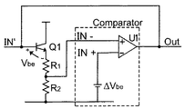
本発明にかかるバンドギャップ電圧基準Vrefを導く実施例について説明する。図4において、バイポーラトランジスタQ1は、Vbeを供給する。バイポーラトランジスタQ1のエミッタは、抵抗R1,R2を含む抵抗分圧器に接続される。分圧器の出力は、コンパレータU1の反転入力に供給される。コンパレータU1の非反転入力には、図2の回路により生成することができるΔVbeを備える電圧源が与えられる。コンパレータの出力は、入力IN’に接続される。この結果、
IN’=OUT
OUT=IN’ΔVbe(図5Bから)
を満たす。
An embodiment for deriving the bandgap voltage reference Vref according to the present invention will be described. In FIG. 4, a bipolar transistor Q1 supplies Vbe. The emitter of bipolar transistor Q1 is connected to a resistor voltage divider including resistors R1 and R2. The output of the voltage divider is provided to the inverting input of comparator U1. The non-inverting input of comparator U1 is provided with a voltage source with ΔVbe that can be generated by the circuit of FIG. The output of the comparator is connected to input IN '. As a result,
IN '= OUT
OUT = IN ' ΔVbe (from FIG. 5B)
Meet.
コンパレータの出力を、IN−,IN’の各々に対して図5A,5Bに示す。図5Aは、IN−、すなわちコンパレータの反転入力に対する出力を示す。図5Bは、IN’、すなわちVbe基準電圧を供給するバイポーラトランジスタQ1の入力に対する出力を示す。コンパレータの出力が入力IN’に接続されているので、出力は、
Vbe+[(R1+R2)/R2]ΔVbe
に等しい。
The output of the comparator is shown in FIGS. 5A and 5B for each of IN− and IN ′. FIG. 5A shows IN-, the output for the inverting input of the comparator. FIG. 5B shows IN ', the output for the input of bipolar transistor Q1 which supplies the Vbe reference voltage. Since the output of the comparator is connected to input IN ', the output is
Vbe + [(R1 + R2) / R2] ΔVbe
be equivalent to.
図6に、図4のΔVbeの代わりにカレントミラー回路の実施例を示す。加えて、コンパレータは、差動増幅器として与えられるFETQ2,Q3およびQ4により実装される。入力IN−,IN’は、トランジスタQ2,Q3のソースに各々供給される。出力OUT=Vrefは、トランジスタQ4のソースから供給される。ΔVbeは、トランジスタQ2,Q3のゲート間のカレントミラーにより供給される。図6において、抵抗R3,R4を含む分圧器が与えられる。 FIG. 6 shows an embodiment of a current mirror circuit instead of ΔVbe in FIG. In addition, the comparator is implemented by FETs Q2, Q3 and Q4 provided as differential amplifiers. The inputs IN- and IN 'are supplied to the sources of the transistors Q2 and Q3, respectively. The output OUT = Vref is supplied from the source of the transistor Q4. ΔVbe is supplied by a current mirror between the gates of the transistors Q2 and Q3. In FIG. 6, a voltage divider including resistors R3 and R4 is provided.
このようにして、回路は、Voutの倍数の基準電圧Vout’を生成する。このことは、1.25Vの基準電圧という非常に低い回路において重要である。 In this way, the circuit generates a reference voltage Vout 'that is a multiple of Vout. This is important in very low circuits, with a reference voltage of 1.25V.
本発明を特定の実施形態に関して説明したが、様々な応用例、変更例および使用法が、当業者には明らかであろう。従って、本発明は、詳細な説明には限定されず、添付の特許請求の範囲に基づく。 Although the present invention has been described with respect to particular embodiments, various applications, modifications and uses will be apparent to those skilled in the art. Therefore, the present invention is not limited to the detailed description, but is based on the appended claims.
Q1〜Q4 トランジスタ
R1〜R5 抵抗
U1 コンパレータ
Q1-Q4 Transistors R1-R5 Resistance U1 Comparator
Claims (3)
2つのバイポーラトランジスタの2つのVbe電圧の差分に比例する第2の電圧ΔVbeを供給する第2の回路と、
VbeとΔVbeに接続された各々の入力および前記第1のバイポーラトランジスタのベースに接続された出力を有するコンパレータとを備え、
これにより、VbeとΔVbeとに定数を乗算し、各々の合計に比例する電圧を、前記コンパレータの出力から供給することを特徴とするバンドギャップ電圧基準回路。 A first circuit for providing a first voltage proportional to Vbe of the first bipolar transistor;
A second circuit for supplying a second voltage ΔVbe proportional to a difference between two Vbe voltages of the two bipolar transistors;
A comparator having respective inputs connected to Vbe and ΔVbe and an output connected to the base of said first bipolar transistor;
The bandgap voltage reference circuit according to claim 1, wherein Vbe and ΔVbe are multiplied by a constant, and a voltage proportional to the sum is supplied from the output of the comparator.
2つのバイポーラトランジスタの各々のVbe電圧間の差分信号を含む差分電圧ΔVbeを供給するカレントミラーを構成するように接続された前記2つのバイポーラトランジスタを含むカレントミラー回路と、
VbeとΔVbeに接続された各々の入力および前記第1のバイポーラトランジスタのベースに接続された出力を有するコンパレータとを備え、
これにより、VbeとΔVbeとに定数を乗算し、各々の合計に比例する電圧を、前記コンパレータの出力から供給することを特徴とするバンドギャップ電圧基準回路。 A first bipolar transistor for supplying a reference voltage Vbe,
A current mirror circuit including the two bipolar transistors connected to form a current mirror that supplies a difference voltage ΔVbe including a difference signal between the Vbe voltages of the two bipolar transistors;
A comparator having respective inputs connected to Vbe and ΔVbe and an output connected to the base of said first bipolar transistor;
The bandgap voltage reference circuit according to claim 1, wherein Vbe and ΔVbe are multiplied by a constant, and a voltage proportional to the sum is supplied from the output of the comparator.
2つのバイポーラトランジスタの2つのVbe電圧の差分に比例する第2の電圧ΔVbeを供給する第2の回路と、
VbeとΔVbeに接続された各々の入力および前記第1のバイポーラトランジスタのベースに接続された出力を有するコンパレータとを備え、
これにより、実質的に温度に依存しない電圧基準を、前記コンパレータの出力から供給することを特徴とするバンドギャップ電圧基準回路。 A first circuit for providing a first voltage proportional to Vbe of the first bipolar transistor;
A second circuit for supplying a second voltage ΔVbe proportional to a difference between two Vbe voltages of the two bipolar transistors;
A comparator having respective inputs connected to Vbe and ΔVbe and an output connected to the base of said first bipolar transistor;
Thus, a voltage reference substantially independent of temperature is supplied from the output of the comparator.
Applications Claiming Priority (2)
| Application Number | Priority Date | Filing Date | Title |
|---|---|---|---|
| US44106303P | 2003-01-17 | 2003-01-17 | |
| US10/713,928 US7164308B2 (en) | 2003-01-17 | 2003-11-14 | Temperature compensated bandgap voltage reference |
Publications (2)
| Publication Number | Publication Date |
|---|---|
| JP2004227584A true JP2004227584A (en) | 2004-08-12 |
| JP2004227584A5 JP2004227584A5 (en) | 2005-09-22 |
Family
ID=32600297
Family Applications (1)
| Application Number | Title | Priority Date | Filing Date |
|---|---|---|---|
| JP2004011119A Pending JP2004227584A (en) | 2003-01-17 | 2004-01-19 | Temperature-compensated bandgap voltage reference circuit |
Country Status (5)
| Country | Link |
|---|---|
| US (1) | US7164308B2 (en) |
| EP (1) | EP1439445B1 (en) |
| JP (1) | JP2004227584A (en) |
| AT (1) | ATE352804T1 (en) |
| DE (1) | DE602004004419T2 (en) |
Cited By (1)
| Publication number | Priority date | Publication date | Assignee | Title |
|---|---|---|---|---|
| US8890187B2 (en) | 2010-04-16 | 2014-11-18 | Semiconductor Energy Laboratory Co., Ltd. | Light-emitting device with an insulating partition |
Families Citing this family (3)
| Publication number | Priority date | Publication date | Assignee | Title |
|---|---|---|---|---|
| US7777561B2 (en) * | 2008-07-30 | 2010-08-17 | Lsi Corporation | Robust current mirror with improved input voltage headroom |
| US8044684B1 (en) | 2010-04-15 | 2011-10-25 | Stmicroelectronics Pvt. Ltd. | Input and output buffer including a dynamic driver reference generator |
| US10120405B2 (en) | 2014-04-04 | 2018-11-06 | National Instruments Corporation | Single-junction voltage reference |
Family Cites Families (10)
| Publication number | Priority date | Publication date | Assignee | Title |
|---|---|---|---|---|
| JPS58221507A (en) | 1982-06-18 | 1983-12-23 | Toshiba Corp | Transistor circuit |
| US5132556A (en) | 1989-11-17 | 1992-07-21 | Samsung Semiconductor, Inc. | Bandgap voltage reference using bipolar parasitic transistors and mosfet's in the current source |
| US5394078A (en) * | 1993-10-26 | 1995-02-28 | Analog Devices, Inc. | Two terminal temperature transducer having circuitry which controls the entire operating current to be linearly proportional with temperature |
| DE19620181C1 (en) | 1996-05-20 | 1997-09-25 | Siemens Ag | Band-gap reference voltage circuit with temp. compensation e.g. for integrated logic circuits |
| US5686823A (en) * | 1996-08-07 | 1997-11-11 | National Semiconductor Corporation | Bandgap voltage reference circuit |
| US6005374A (en) * | 1997-04-02 | 1999-12-21 | Telcom Semiconductor, Inc. | Low cost programmable low dropout regulator |
| US6121824A (en) * | 1998-12-30 | 2000-09-19 | Ion E. Opris | Series resistance compensation in translinear circuits |
| US6181121B1 (en) * | 1999-03-04 | 2001-01-30 | Cypress Semiconductor Corp. | Low supply voltage BICMOS self-biased bandgap reference using a current summing architecture |
| JP4674947B2 (en) | 2000-09-29 | 2011-04-20 | オリンパス株式会社 | Constant voltage output circuit |
| US6288525B1 (en) * | 2000-11-08 | 2001-09-11 | Agere Systems Guardian Corp. | Merged NPN and PNP transistor stack for low noise and low supply voltage bandgap |
-
2003
- 2003-11-14 US US10/713,928 patent/US7164308B2/en not_active Expired - Fee Related
-
2004
- 2004-01-17 DE DE602004004419T patent/DE602004004419T2/en not_active Expired - Lifetime
- 2004-01-17 EP EP04001170A patent/EP1439445B1/en not_active Expired - Lifetime
- 2004-01-17 AT AT04001170T patent/ATE352804T1/en not_active IP Right Cessation
- 2004-01-19 JP JP2004011119A patent/JP2004227584A/en active Pending
Cited By (1)
| Publication number | Priority date | Publication date | Assignee | Title |
|---|---|---|---|---|
| US8890187B2 (en) | 2010-04-16 | 2014-11-18 | Semiconductor Energy Laboratory Co., Ltd. | Light-emitting device with an insulating partition |
Also Published As
| Publication number | Publication date |
|---|---|
| DE602004004419D1 (en) | 2007-03-15 |
| EP1439445B1 (en) | 2007-01-24 |
| DE602004004419T2 (en) | 2007-11-15 |
| US7164308B2 (en) | 2007-01-16 |
| ATE352804T1 (en) | 2007-02-15 |
| US20040140844A1 (en) | 2004-07-22 |
| EP1439445A3 (en) | 2005-06-08 |
| EP1439445A2 (en) | 2004-07-21 |
Similar Documents
| Publication | Publication Date | Title |
|---|---|---|
| JP4817825B2 (en) | Reference voltage generator | |
| JP4809340B2 (en) | Voltage circuit proportional to absolute temperature | |
| JP3039454B2 (en) | Reference voltage generation circuit | |
| US7511567B2 (en) | Bandgap reference voltage circuit | |
| JP5085238B2 (en) | Reference voltage circuit | |
| US20060038608A1 (en) | Band-gap circuit | |
| JPH0561558A (en) | Reference voltage generating circuit | |
| JP2007133533A (en) | Reference voltage generation circuit | |
| JP2005182113A (en) | Reference voltage generating circuit | |
| JP2008271503A (en) | Reference current circuit | |
| JP5434695B2 (en) | Band gap circuit, low voltage detection circuit and regulator circuit | |
| JP2007095031A (en) | Band gap reference voltage generation circuit for low voltage | |
| JP2004227584A (en) | Temperature-compensated bandgap voltage reference circuit | |
| JPH1124769A (en) | Constant current circuit | |
| JP4677735B2 (en) | Constant current source circuit | |
| JP4314669B2 (en) | Bandgap reference circuit | |
| JP2005182731A (en) | Temperature-compensated bandgap voltage reference circuit | |
| JP2005222497A (en) | Band gap voltage reference circuit with temperature compensation | |
| KR100599974B1 (en) | Voltage reference generator | |
| JP2006031246A (en) | Reference current generation circuit | |
| JP2729001B2 (en) | Reference voltage generation circuit | |
| JP2006244228A (en) | Power source circuit | |
| JP2000134045A (en) | Voltage-to-current conversion circuit | |
| JP3391293B2 (en) | n-th power circuit | |
| JP4445916B2 (en) | Band gap circuit |
Legal Events
| Date | Code | Title | Description |
|---|---|---|---|
| A521 | Request for written amendment filed |
Free format text: JAPANESE INTERMEDIATE CODE: A523 Effective date: 20050624 |
|
| A131 | Notification of reasons for refusal |
Free format text: JAPANESE INTERMEDIATE CODE: A131 Effective date: 20060428 |
|
| A521 | Request for written amendment filed |
Free format text: JAPANESE INTERMEDIATE CODE: A523 Effective date: 20060728 |
|
| A131 | Notification of reasons for refusal |
Free format text: JAPANESE INTERMEDIATE CODE: A131 Effective date: 20070119 |
|
| A601 | Written request for extension of time |
Free format text: JAPANESE INTERMEDIATE CODE: A601 Effective date: 20070419 |
|
| A602 | Written permission of extension of time |
Free format text: JAPANESE INTERMEDIATE CODE: A602 Effective date: 20070424 |
|
| A601 | Written request for extension of time |
Free format text: JAPANESE INTERMEDIATE CODE: A601 Effective date: 20070521 |
|
| A602 | Written permission of extension of time |
Free format text: JAPANESE INTERMEDIATE CODE: A602 Effective date: 20070524 |
|
| A601 | Written request for extension of time |
Free format text: JAPANESE INTERMEDIATE CODE: A601 Effective date: 20070619 |
|
| A602 | Written permission of extension of time |
Free format text: JAPANESE INTERMEDIATE CODE: A602 Effective date: 20070622 |
|
| A521 | Request for written amendment filed |
Free format text: JAPANESE INTERMEDIATE CODE: A523 Effective date: 20070719 |
|
| A02 | Decision of refusal |
Free format text: JAPANESE INTERMEDIATE CODE: A02 Effective date: 20080205 |
|
| RD13 | Notification of appointment of power of sub attorney |
Free format text: JAPANESE INTERMEDIATE CODE: A7433 Effective date: 20080508 |
|
| A521 | Request for written amendment filed |
Free format text: JAPANESE INTERMEDIATE CODE: A821 Effective date: 20080508 |
|
| A521 | Request for written amendment filed |
Free format text: JAPANESE INTERMEDIATE CODE: A523 Effective date: 20080606 |
|
| A911 | Transfer to examiner for re-examination before appeal (zenchi) |
Free format text: JAPANESE INTERMEDIATE CODE: A911 Effective date: 20080611 |
|
| A912 | Re-examination (zenchi) completed and case transferred to appeal board |
Free format text: JAPANESE INTERMEDIATE CODE: A912 Effective date: 20081212 |