JP2004201409A - Power module - Google Patents
Power module Download PDFInfo
- Publication number
- JP2004201409A JP2004201409A JP2002366812A JP2002366812A JP2004201409A JP 2004201409 A JP2004201409 A JP 2004201409A JP 2002366812 A JP2002366812 A JP 2002366812A JP 2002366812 A JP2002366812 A JP 2002366812A JP 2004201409 A JP2004201409 A JP 2004201409A
- Authority
- JP
- Japan
- Prior art keywords
- voltage
- arm
- load
- terminals
- motor
- Prior art date
- Legal status (The legal status is an assumption and is not a legal conclusion. Google has not performed a legal analysis and makes no representation as to the accuracy of the status listed.)
- Withdrawn
Links
Images


Abstract
Description
【0001】
【発明の属する技術分野】
この発明は、直流電源からの直流電圧を昇圧してモータを駆動するパワーモジュールに関し、特に、信頼性が高いパワーモジュールに関するものである。
【0002】
【従来の技術】
最近、環境に配慮した自動車としてハイブリッド自動車(Hybrid Vehicle)が大きな注目を集めている。そして、ハイブリッド自動車は、一部、実用化されている。
【0003】
このハイブリッド自動車は、従来のエンジンに加え、直流電源とインバータとインバータによって駆動されるモータとを動力源とする自動車である。つまり、エンジンを駆動することにより動力源を得るとともに、直流電源からの直流電圧をインバータによって交流電圧に変換し、その変換した交流電圧によりモータを回転することによって動力源を得るものである。
【0004】
このようなハイブリッド自動車は、たとえば、図4に示すようなモータ駆動装置300を搭載している。図4を参照して、モータ駆動装置300は、直流電源B1と、昇圧コンバータ310と、コンデンサ320と、インバータ330,340とを備える。
【0005】
昇圧コンバータ310は、NPNトランジスタ311,312と、ダイオード313,314と、リアクトルL1とを含む。
【0006】
リアクトルL1は、一方端が直流電源B1に接続され、他方端がNPNトランジスタ311とNPNトランジスタ312との中間点に接続される。
【0007】
NPNトランジスタ311,312は、インバータ330,340の電源ラインとアースラインとの間に直列に接続される。NPNトランジスタ311は、コレクタが電源ラインに接続され、エミッタがNPNトランジスタ312のコレクタに接続される。NPNトランジスタ312のエミッタは、アースラインに接続される。
【0008】
ダイオード313,314は、エミッタからコレクタへ電流が流れるようにそれぞれNPNトランジスタ311,312に並列に接続される。
【0009】
コンデンサ320は、ノードN1とノードN2との間に接続される。
インバータ330は、U相アーム330Aと、V相アーム330Bと、W相アーム330Cとを含む。U相アーム330A,V相アーム330BおよびW相アーム330Cは、ノードN1とノードN2との間に並列に接続される。
【0010】
U相アーム330Aは、直列接続されたNPNトランジスタ331,332から成る。V相アーム330Bは、直列接続されたNPNトランジスタ333,334から成る。W相アーム330Cは、直列接続されたNPNトランジスタ335,336から成る。
【0011】
NPNトランジスタ331,333,335のコレクタは、電源ラインに接続される。NPNトランジスタ332,334,336のエミッタは、アースラインに接続される。NPNトランジスタ331,333,335のエミッタは、それぞれ、NPNトランジスタ332,334,336のコレクタに接続される。
【0012】
NPNトランジスタ331〜336には、エミッタ側からコレクタ側へ電流が流れるように、それぞれ、ダイオードD337〜339,341〜343が接続されている。
【0013】
NPNトランジスタ331とNPNトランジスタ332との中間点、すなわち、NPNトランジスタ331のエミッタおよびNPNトランジスタ332のコレクタは、交流モータM1のU相コイルの一方端に接続される。また、NPNトランジスタ333とNPNトランジスタ334との中間点、すなわち、NPNトランジスタ333のエミッタおよびNPNトランジスタ334のコレクタは、交流モータM1のV相コイルの一方端に接続される。さらに、NPNトランジスタ335とNPNトランジスタ336との中間点、すなわち、NPNトランジスタ335のエミッタおよびNPNトランジスタ336のコレクタは、交流モータM1のW相コイルの一方端に接続される。
【0014】
インバータ340は、U相アーム340Aと、V相アーム340Bと、W相アーム340Cとを含む。U相アーム340A,V相アーム340BおよびW相アーム340Cは、ノードN1とノードN2との間に並列に接続される。
【0015】
U相アーム340Aは、直列接続されたNPNトランジスタ344,345から成る。V相アーム340Bは、直列接続されたNPNトランジスタ346,347から成る。W相アーム340Cは、直列接続されたNPNトランジスタ348,349から成る。
【0016】
NPNトランジスタ344,346,348のコレクタは、電源ラインに接続される。NPNトランジスタ345,347,349のエミッタは、アースラインに接続される。NPNトランジスタ344,346,348のエミッタは、それぞれ、NPNトランジスタ345,347,349のコレクタに接続される。
【0017】
NPNトランジスタ344〜349には、エミッタ側からコレクタ側へ電流が流れるように、それぞれ、ダイオードD350〜355が接続されている。
【0018】
NPNトランジスタ344とNPNトランジスタ345との中間点、すなわち、NPNトランジスタ344のエミッタおよびNPNトランジスタ345のコレクタは、交流モータM2のU相コイルの一方端に接続される。また、NPNトランジスタ346とNPNトランジスタ347との中間点、すなわち、NPNトランジスタ346のエミッタおよびNPNトランジスタ347のコレクタは、交流モータM2のV相コイルの一方端に接続される。さらに、NPNトランジスタ348とNPNトランジスタ349との中間点、すなわち、NPNトランジスタ348のエミッタおよびNPNトランジスタ349のコレクタは、交流モータM2のW相コイルの一方端に接続される。
【0019】
直流電源B1は、直流電圧を出力する。昇圧コンバータ310は、NPNトランジスタ311,312がオン/オフされることにより、直流電源B1から出力された直流電圧の電圧レベルを昇圧してコンデンサ320へ出力する。すなわち、昇圧コンバータ310は、NPNトランジスタ312がオンされた期間に応じてリアクトルL1に電力を蓄積し、その蓄積した電力に応じた直流電圧をコンデンサ320へ出力する。
【0020】
コンデンサ320は、昇圧コンバータ310から出力された直流電圧を受け、その受けた直流電圧を平滑化してインバータ330,340へ供給する。
【0021】
インバータ330は、昇圧コンバータ310から受けた直流電圧を交流電圧に変換し、その変換した交流電圧によって交流モータM1を駆動する。また、インバータ340は、昇圧コンバータ310から受けた直流電圧を交流電圧に変換し、その変換した交流電圧によって交流モータM2を駆動する。
【0022】
このように、モータ駆動装置300は、直流電源B1から出力された直流電圧を昇圧し、その昇圧した直流電圧を交流電圧に変換して交流モータM1,M2を駆動する。
【0023】
また、発電機を駆動するインバータと電動機を駆動するインバータとを含む駆動システムが特開平8−79914号公報に開示されている。そして、この駆動システムにおいては、発電機により発電された交流電圧をバッテリ側へ供給する回生制動時に、インバータが発電機の1つのコイルを用いて昇圧回生制動を行なう。
【0024】
【特許文献1】
特開平8−79914号公報
【0025】
【特許文献2】
特開昭64−77153号公報
【0026】
【特許文献3】
特開2000−156937号公報
【0027】
【特許文献4】
特開2002−272121号公報
【0028】
【発明が解決しようとする課題】
従来のモータ駆動装置300に含まれる昇圧コンバータ310、およびインバータ330,340は、直列接続された2つのNPNトランジスタを用いて構成される。
【0029】
しかし、直流電圧を昇圧する昇圧コンバータ310に用いられるNPNトランジスタ311,312は、インバータ330,340に用いられるNPNトランジスタ331〜336,344〜349よりも熱ストレスが大きく、昇圧コンバータ310に用いられたNPNトランジスタ311,312の寿命が短くなるという問題がある。
【0030】
そこで、この発明は、かかる問題を解決するためになされたものであり、その目的は、信頼性の高いパワーモジュールを提供することである。
【0031】
【課題を解決するための手段および発明の効果】
この発明によれば、パワーモジュールは、複数のアームと、複数のアーム端子、複数の負荷端子と、切換手段とを備える。複数のアームは、各々が直列接続された第1および第2のスイッチング素子を含む。複数のアーム端子は、複数のアームに対応して設けられ、各々が対応するアームに含まれる第1のスイッチング素子と第2のスイッチング素子との中間点に接続される。複数の負荷端子は、複数のアーム端子に対応して設けられ、各々が負荷に接続される。切換手段は、特定の負荷に接続された負荷端子とアーム端子との接続時間が複数のアーム端子間でほぼ等しくなるように複数のアーム端子と複数の負荷端子との接続を切換える。
【0032】
好ましくは、切換手段は、一定時間ごとに複数のアーム端子と複数の負荷端子との接続を切換える。
【0033】
好ましくは、切換手段は、所定の順序に従って複数のアーム端子と複数の負荷端子との接続を切換える。
【0034】
好ましくは、特定の負荷は、負荷端子をアーム端子に接続したときの第1および第2のスイッチング素子の熱ストレスが最大となる負荷である。
【0035】
好ましくは、特定の負荷は、一方端子が直流電源に接続され、他方端子が複数の負荷端子に含まれる特定負荷端子に接続されるリアクトルである。
【0036】
好ましくは、リアクトルおよび特定負荷端子に接続されたアームは、直流電源からの直流電圧を昇圧して他のアームに供給する。
【0037】
好ましくは、特定負荷端子以外の負荷端子は、モータの端子に接続される。
好ましくは、モータは、車両の駆動輪を駆動するためのモータである。
【0038】
好ましくは、複数のアームは、3n+1(nは自然数)個のアームであり、複数のアーム端子は、3n+1個のアーム端子であり、複数の負荷端子は、3n+1個の負荷端子であり、リアクトルおよび特定負荷端子に接続された1つのアームは、直流電源から出力された直流電圧を昇圧して出力するコンバータを構成し、1つのアームを除く3n個のアームは、少なくとも1個のモータを駆動する少なくとも1個のインバータを構成し、少なくとも1個のインバータは、コンバータにより昇圧された直流電圧を受け、その受けた直流電圧を交流電圧に変換して少なくとも1つのモータを駆動する。
【0039】
好ましくは、少なくとも1つのインバータは、第1および第2のインバータから成り、少なくとも1つのモータは、第1および第2のモータから成り、第1のインバータは、コンバータにより昇圧された直流電源を交流電圧に変換して第1のモータを駆動し、第2のインバータは、第2のモータが発電した交流電圧を直流電圧に変換して前記コンバータへ供給し、コンバータは、第2のインバータから供給された交流電圧を降圧して直流電源に供給する。
【0040】
この発明によるパワーモジュールにおいては、最大の負荷に接続される各アームの接続時間が複数のアーム間でほぼ等しくなるように、複数のアームに対応して設けられた複数のアーム端子と複数のアーム端子に対応して設けられた複数の負荷端子との接続が切換えられる。
【0041】
したがって、複数のアームに含まれる複数のスイッチング素子における熱ストレスをほぼ均等にできる。その結果、パワーモジュールの寿命を長くできる。
【0042】
【発明の実施の形態】
本発明の実施の形態について図面を参照しながら詳細に説明する。なお、図中同一または相当部分には同一符号を付してその説明は繰返さない。
【0043】
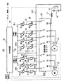
図1を参照して、この発明の実施の形態によるパワーモジュール100は、直流電源Bと、電圧センサー10,11と、リアクトルL1と、コンデンサC1と、アーム13〜19と、負荷切換ユニット20と、電流センサー21,22と、制御装置30とを備える。
【0044】
アーム13〜19は、電源ラインBL1とアースラインBL2との間に並列に接続される。アーム13は、直列接続されたNPNトランジスタQ1,Q2から成る。アーム14は、直列接続されたNPNトランジスタQ3,Q4から成る。アーム15は、直列接続されたNPNトランジスタQ5,Q6から成る。
【0045】
アーム16は、直列接続されたNPNトランジスタQ7,Q8から成る。アーム17は、直列接続されたNPNトランジスタQ9,Q10から成る。アーム18は、直列接続されたNPNトランジスタQ11,Q12から成る。アーム19は、直列接続されたNPNトランジスタQ13,Q14から成る。
【0046】
NPNトランジスタQ1,Q3,Q5,Q7,Q9,Q11,Q13の各々は、コレクタが電源ラインBL1に接続され、エミッタがそれぞれNPNトランジスタQ2,Q4,Q6,Q8,Q10,Q12,Q14のコレクタに接続される。NPNトランジスタQ2,Q4,Q6,Q8,Q10,Q12,Q14のエミッタはアースラインBL2に接続される。
【0047】
NPNトランジスタQ1〜Q14は、エミッタ側からコレクタ側へ電流が流れるように、それぞれ、ダイオードD1〜D14が接続されている。
【0048】
なお、NPNトランジスタQ1〜Q14は、相互に同じ特性を有する。
コンデンサC1は、電源ラインBL1とアースラインBL2との間にアーム13〜19に並列に接続される。
【0049】
リアクトルL1は、その一方端が負荷切換ユニット20の負荷端子DUに接続され、他方端が直流電源Bの正電極に接続される。
【0050】
負荷切換ユニット20は、アーム端子1〜7と、負荷端子DU,U1,U2,V1,V2,W1,W2とを有する。
【0051】
アーム端子1は、NPNトランジスタQ1とNPNトランジスタQ2との中間点、すなわち、NPNトランジスタQ1のエミッタとNPNトランジスタQ2のコレクタとに接続される。アーム端子2は、NPNトランジスタQ3とNPNトランジスタQ4との中間点、すなわち、NPNトランジスタQ3のエミッタとNPNトランジスタQ4のコレクタとに接続される。アーム端子3は、NPNトランジスタQ5とNPNトランジスタQ6との中間点、すなわち、NPNトランジスタQ5のエミッタとNPNトランジスタQ6のコレクタとに接続される。
【0052】
アーム端子4は、NPNトランジスタQ7とNPNトランジスタQ8との中間点、すなわち、NPNトランジスタQ7のエミッタとNPNトランジスタQ8のコレクタとに接続される。アーム端子5は、NPNトランジスタQ9とNPNトランジスタQ10との中間点、すなわち、NPNトランジスタQ9のエミッタとNPNトランジスタQ10のコレクタとに接続される。アーム端子6は、NPNトランジスタQ11とNPNトランジスタQ12との中間点、すなわち、NPNトランジスタQ11のエミッタとNPNトランジスタQ12のコレクタとに接続される。アーム端子7は、NPNトランジスタQ13とNPNトランジスタQ14との中間点、すなわち、NPNトランジスタQ13のエミッタとNPNトランジスタQ14のコレクタとに接続される。
【0053】
負荷端子DUは、リアクトルL1の一方端に接続される。負荷端子U1,V1,W1は、それぞれ、交流モータM1のU相、V相、W相に接続される。負荷端子U2,V2,W2は、それぞれ、交流モータM2のU相、V相、W相に接続される。
【0054】
交流モータM1,M2は、ハイブリッド自動車の駆動輪を駆動するためのトルクを発生するための駆動モータである。あるいは、これらのモータはエンジンにて駆動される発電機の機能を持つように、そして、エンジンに対して電動機として動作し、たとえば、エンジン始動を行ない得るようなものとしてハイブリッド自動車に組み込まれるようにしてもよい。
【0055】
直流電源Bは、ニッケル水素またはリチウムイオン等の二次電池から成る。電圧センサー10は、直流電源Bから出力される直流電圧Vbを検出し、その検出した直流電圧Vbを制御装置30へ出力する。
【0056】
リアクトルL1は、直流電源Bから出力される直流電流に応じた電力を蓄積する。コンデンサC1は、電源ラインBL1とアースラインBL2との間に印加される直流電圧を平滑化する。電圧センサー11は、コンデンサC1の両端の電圧Vmを検出し、その検出した電圧Vmを制御装置30へ出力する。
【0057】
負荷切換ユニット20は、制御装置30からの切換信号EXCに応じて、アーム端子1〜7と負荷端子DU,U1,U2,V1,V2,W1,W2との接続を切換える。より具体的には、負荷切換ユニット20は、アーム端子1〜7の各々が負荷端子DUに接続される接続時間がほぼ等しくなるように、アーム端子1〜7と負荷端子DU,U1,U2,V1,V2,W1,W2との接続を切換える。
【0058】
アーム端子1が負荷端子DUに接続されているとき、リアクトルL1およびアーム13は昇圧コンバータCVを構成する。また、アーム端子2〜4がそれぞれ負荷端子U1,V1,W1に接続されているとき、アーム14〜16は、交流モータM1を駆動するインバータIVT1を構成する。さらに、アーム端子5〜7がそれぞれ負荷端子U2,V2,W2に接続されているとき、アーム17〜19は、交流モータM2を駆動するインバータIVT2を構成する。
【0059】
一般的には、アーム端子1が負荷端子DUに接続されているとき、インバータIVT1は、アーム14〜19から任意に選択された3つのアームにより構成され、インバータIVT2は、アーム14〜19のうちインバータIVT1を構成する3つのアーム以外の3つのアームにより構成される。たとえば、インバータIVT1は、アーム14,17,18により構成され、インバータIVT2は、アーム15,16,19により構成される。
【0060】
また、昇圧コンバータCVを構成するアームは、アーム13に限らず、アーム13〜19から任意に選択された1つのアームにより構成される。
【0061】
したがって、負荷切換ユニット20は、制御装置30から切換信号EXCを受けると、負荷端子DUに接続すべき1つのアームを決定し、次に、負荷端子U1,V1,W1,U2,V2,W2に接続すべき6つのアームを決定する。たとえば、負荷切換ユニット20は、負荷端子DUに接続するアーム端子をアーム端子1→アーム端子2→アーム端子3→アーム端子4→アーム端子5→アーム端子6→アーム端子7→アーム端子1・・・の順序で切換える。そして、負荷切換ユニット20は、これに伴って負荷端子U1,V1,W1,U2,V2,W2に接続するアーム端子を、負荷端子DUに接続するアーム端子の切換方向と同じ方向に従って順次切換える。そして、負荷切換ユニット20は、制御装置30から信号EXCを受けるごとに、アーム端子1〜7と負荷端子DU,U1,V1,W1,U2,V2,W2との接続を1回切換える。
【0062】
昇圧コンバータCVは、制御装置30から信号PWMUを受けると、直流電源Bからの直流電圧Vbを昇圧して電源ラインBL1とアースラインBL2との間に供給する。また、昇圧コンバータCVは、制御装置30から信号PWMDを受けると、インバータIVT1またはIVT2から供給された直流電圧を降圧して直流電源Bに供給する。
【0063】
インバータIVT1は、コンデンサC1を介して昇圧コンバータCVから直流電圧が供給されると制御装置30からの信号PWMI1に基づいて直流電圧を交流電圧に変換して交流モータM1を駆動する。これにより、交流モータM1は、トルク指令値TR1によって指定されたトルクを発生するように駆動される。また、インバータIVT1は、パワーモジュール100が搭載されたハイブリッド自動車または電気自動車の回生制動時、交流モータM1が発電した交流電圧を制御装置30からの信号PWMC1に基づいて直流電圧に変換し、その変換した直流電圧をコンデンサC1を介して昇圧コンバータCVへ供給する。
【0064】
インバータIVT2は、コンデンサC1を介して昇圧コンバータCVから直流電圧が供給されると制御装置30からの信号PWMI2に基づいて直流電圧を交流電圧に変換して交流モータM2を駆動する。これにより、交流モータM2は、トルク指令値TR2によって指定されたトルクを発生するように駆動される。また、インバータIVT2は、パワーモジュール100が搭載されたハイブリッド自動車または電気自動車の回生制動時、交流モータM2が発電した交流電圧を制御装置30からの信号PWMC2に基づいて直流電圧に変換し、その変換した直流電圧をコンデンサC1を介して昇圧コンバータCVへ供給する。
【0065】
なお、ここで言う回生制動とは、ハイブリッド自動車または電気自動車を運転するドライバーによるフットブレーキ操作があった場合の回生発電を伴う制動や、フットブレーキを操作しないものの、走行中にアクセルペダルをオフすることで回生発電をさせながら車両を減速(または加速の中止)させることを含む。
【0066】
電流センサー21は、交流モータM1の各相に流れるモータ電流MCRT1を検出し、その検出したモータ電流MCRT1を制御装置30へ出力する。電流センサー22は、交流モータM2の各相に流れるモータ電流MCRT2を検出し、その検出したモータ電流MCRT2を制御装置30へ出力する。
【0067】
制御装置30は、外部に設けられたECU(Electrical Control Unit)からトルク指令値TR1,2およびモータ回転数MRN1,2を受け、電圧センサー10から直流電圧Vbを受け、電圧センサー11から電圧Vmを受け、電流センサー21からモータ電流MCRT1を受け、電流センサー22からモータ電流MCRT2を受ける。そして、制御装置30は、直流電圧Vb、電圧Vm、モータ電流MCRT1、トルク指令値TR1およびモータ回転数MRN1に基づいて、後述する方法によりインバータIVT1が交流モータM1を駆動するときにインバータIVT1を構成するNPNトランジスタをスイッチング制御するための信号PWMI1を生成し、その生成した信号PWMI1をインバータIVT1へ出力する。
【0068】
また、制御装置30は、直流電圧Vb、電圧Vm、モータ電流MCRT2、トルク指令値TR2およびモータ回転数MRN2に基づいて、後述する方法によりインバータIVT2が交流モータM2を駆動するときにインバータIVT2を構成するNPNトランジスタをスイッチング制御するための信号PWMI2を生成し、その生成した信号PWMI2をインバータIVT2へ出力する。
【0069】
さらに、制御装置30は、インバータIVT1(またはIVT2)が交流モータM1(またはM2)を駆動するとき直流電圧Vb、電圧Vm、モータ電流MCRT1(またはMCRT2)、トルク指令値TR1(またはTR2)およびモータ回転数MRN1(またはMRN2)に基づいて、後述する方法により、昇圧コンバータCVを構成するNPNトランジスタをスイッチング制御するための信号PWMUを生成し、その生成した信号PWMUを昇圧コンバータCVへ出力する。
【0070】
さらに、制御装置30は、ハイブリッド自動車または電気自動車が回生制動モードに入ったことを示す信号RGEを外部ECUから受けると、交流モータM1またはM2で発電された交流電圧を直流電圧に変換するための信号PWMC1,2を生成し、その生成した信号PWMC1をインバータIVT1へ出力し、信号PWMC2をインバータIVT2へ出力する。そして、インバータIVT1,2を構成するNPNトランジスタは、信号PWMC1,2によってスイッチング制御される。これにより、インバータIVT1は、交流モータM1で発電された交流電圧を直流電圧に変換して昇圧コンバータCVへ供給し、インバータIVT2は、交流モータM2で発電された交流電圧を直流電圧に変換して昇圧コンバータCVへ供給する。
【0071】
さらに、制御装置30は、ハイブリッド自動車または電気自動車が回生制動モードに入ったことを示す信号RGEを外部ECUから受けると、インバータIVT1,2から供給された直流電圧を降圧するための信号PWMDを生成し、その生成した信号PWMDを昇圧コンバータCVへ出力する。これにより、交流モータM1またはM2が発電した交流電圧は、直流電圧に変換され、降圧されて直流電源Bに供給される。
【0072】
図2は、制御装置30の機能ブロック図である。図2を参照して、制御装置30は、モータトルク制御手段301と、電圧変換制御手段302と、切換手段303とを含む。
【0073】
モータトルク制御手段301は、トルク指令値TR1,2(車両におけるアクセルペダルの踏み込み度合い、ハイブリッド車両においてはエンジンの動作状態をも考慮しながらモータに与えるべきトルク指令を演算して得られている)、直流電源Bの出力電圧Vb、モータ電流MCRT1,2、モータ回転数MRN1,2および昇圧コンバータCVの出力電圧Vmに基づいて、交流モータM1またはM2の駆動時、後述する方法により昇圧コンバータCVを構成するNPNトランジスタをオン/オフするための信号PWMUと、インバータIVT1を構成するNPNトランジスタをオン/オフするための信号PWMI1と、インバータIVT2を構成するNPNトランジスタをオン/オフするための信号PWMI2とを生成し、その生成した信号PWMUを昇圧コンバータCVへ出力し、信号PWMI1をインバータIVT1へ出力し、信号PWMI2をインバータIVT2へ出力する。
【0074】
電圧変換制御手段302は、回生制動時、ハイブリッド自動車または電気自動車が回生制動モードに入ったことを示す信号RGEを外部ECUから受けると、交流モータM1,M2が発電した交流電圧を直流電圧に変換するための信号PWMC1,2を生成してそれぞれインバータIVT1,IVT2へ出力する。
【0075】
また、電圧変換制御手段302は、回生制動時、信号RGEを外部ECUから受けると、インバータIVT1,IVT2から供給された直流電圧を降圧するための信号PWMDを生成して昇圧コンバータCVへ出力する。このように、昇圧コンバータCVは、直流電圧を降圧するための信号PWMDにより電圧を降下させることもできるので、双方向コンバータの機能を有するものである。
【0076】
切換手段303は、一定時間ごとに切換信号EXCを生成して負荷切換ユニット20へ出力する。なお、切換手段303は、たとえば、一定時間を内蔵したタイマーにより計測する。
【0077】
図3は、モータトルク制御手段301の機能ブロック図である。図3を参照して、モータトルク制御手段301は、モータ制御用相電圧演算部40と、インバータ用PWM信号変換部42と、インバータ入力電圧指令演算部50と、フィードバック電圧指令演算部52と、デューティー比変換部54とを含む。
【0078】
モータ制御用相電圧演算部40は、昇圧コンバータCVの出力電圧Vm、すなわち、インバータIVT1,IVT2への入力電圧を電圧センサー11から受け、交流モータM1,M2の各相に流れるモータ電流MCRT1,2を電流センサー21,22から受け、トルク指令値TR1,2を外部ECUから受ける。そして、モータ制御用相電圧演算部40は、これらの入力される信号に基づいて、交流モータM1,M2の各相のコイルに印加する電圧を計算し、その計算した結果をインバータ用PWM信号変換部42へ供給する。インバータ用PWM信号変換部42は、モータ制御用相電圧演算部40から受けた計算結果に基づいて、実際にインバータIVT1,IVT2を構成する各NPNトランジスタをオン/オフする信号PWMI1,2を生成し、その生成した信号PWMI1,2をそれぞれインバータIVT1,IVT2を構成する各NPNトランジスタへ出力する。
【0079】
これにより、インバータIVT1,IVT2を構成する各NPNトランジスタは、スイッチング制御され、交流モータM1,M2が指令されたトルクを出力するように交流モータM1,M2の各相に流す電流を制御する。このようにして、モータ駆動電流が制御され、トルク指令値TR1,2に応じたモータトルクが出力される。
【0080】
一方、インバータ入力電圧指令演算部50は、トルク指令値TR1,2およびモータ回転数MRN1,2に基づいてインバータ入力電圧の最適値(目標値)、すなわち、電圧指令を演算し、その演算した電圧指令をフィードバック電圧指令演算部52へ出力する。
【0081】
フィードバック電圧指令演算部52は、電圧センサー11からの電圧Vmと、インバータ入力電圧指令演算部50からの電圧指令とに基づいて、フィードバック電圧指令を演算し、その演算したフィードバック電圧指令をデューティー比変換部54へ出力する。
【0082】
デューティー比変換部54は、電圧センサー10からのバッテリ電圧Vbと、フィードバック電圧指令演算部52からのフィードバック電圧指令とに基づいて、電圧センサー11からの電圧Vmを、フィードバック電圧指令演算部52からのフィードバック電圧指令に設定するためのデューティー比を演算し、その演算したデューティー比に基づいて昇圧コンバータCVを構成するNPNトランジスタをオン/オフするための信号PWMUを生成する。そして、デューティー比変換部54は、生成した信号PWMUを昇圧コンバータCVを構成するNPNトランジスタへ出力する。
【0083】
なお、昇圧コンバータCVを構成するアームの下側のNPNトランジスタのオンデューティーを大きくすることによりリアクトルL1における電力蓄積が大きくなるため、より高電圧の出力を得ることができる。一方、上側のNPNトランジスタのオンデューティーを大きくすることにより電源ラインBL1の電圧が下がる。そこで、昇圧コンバータCVを構成する2つのNPNトランジスタのデューティー比を制御することで、電源ラインBL1の電圧を直流電源Bの出力電圧以上の任意の電圧に制御可能である。
【0084】
再び、図1を参照して、パワーモジュール100における全体動作について説明する。全体の動作が開始されると、制御装置30は、切換信号EXCを生成して負荷切換ユニット20へ出力する。そして、負荷切換ユニット20は、制御装置30からの切換信号EXCに応じて、アーム端子1〜7と負荷端子DU,U1,V1,W1,U2,V2,W2との接続を上述した方法によって切換える。これにより、昇圧コンバータCVおよびインバータIVT1,IVT2が構成される。直流電源Bは直流電圧Vbを昇圧コンバータCVへ出力する。
【0085】
電圧センサー10は、直流電源Bから出力される直流電圧Vbを検出し、その検出した直流電圧Vbを制御装置30へ出力する。また、電圧センサー11は、コンデンサC1の両端の電圧Vmを検出し、その検出した電圧Vmを制御装置30へ出力する。さらに、電流センサー21は、交流モータM1に流れるモータ電流MCRT1を検出して制御装置30へ出力し、電流センサー22は、交流モータM2に流れるモータ電流MCRT2を検出して制御装置30へ出力する。そして、制御装置30は、外部ECUからトルク指令値TR1,2、およびモータ回転数MRN1,2を受ける。
【0086】
そうすると、制御装置30は、直流電圧Vb、電圧Vm、モータ電流MCRT1、トルク指令値TR1およびモータ回転数MRN1に基づいて、上述した方法により信号PWMI1を生成し、その生成した信号PWMI1をインバータIVT1へ出力する。また、制御装置30は、直流電圧Vb、電圧Vm、モータ電流MCRT2、トルク指令値TR2およびモータ回転数MRN2に基づいて、上述した方法により信号PWMI2を生成し、その生成した信号PWMI2をインバータIVT2へ出力する。さらに、制御装置30は、インバータIVT1(またはIVT2)が交流モータM1(またはM2)を駆動するとき、直流電圧Vb、電圧Vm、モータ電流MCRT1(またはMCRT2)、トルク指令値TR1(またはTR2)、およびモータ回転数MRN1(またはMRN2)に基づいて、上述した方法により昇圧コンバータCVを構成する2つのNPNトランジスタをスイッチング制御するための信号PWMUを生成し、その生成した信号PWMUを昇圧コンバータCVへ出力する。
【0087】
そうすると、昇圧コンバータCVは、信号PWMUに応じて、直流電源Bからの直流電圧を昇圧し、その昇圧した直流電圧を電源ラインBL1とアースラインBL2との間に供給する。そして、インバータIVT1は、コンデンサC1によって平滑化された直流電圧を制御装置30からの信号PWMI1によって交流電圧に変換して交流モータM1を駆動する。また、インバータIVT2は、コンデンサC1によって平滑化された直流電圧を制御装置30からの信号PWMI2によって交流電圧に変換して交流モータM2を駆動する。これによって、交流モータM1は、トルク指令値TR1によって指定されたトルクを発生し、交流モータM2は、トルク指令値TR2によって指定されたトルクを発生する。
【0088】
また、パワーモジュール100が搭載されたハイブリッド自動車または電気自動車の回生制動時、制御装置30は、外部ECUから信号RGEを受け、その受けた信号RGEに応じて、信号PWMC1,2を生成してそれぞれインバータIVT1,IVT2へ出力し、信号PWMDを生成して昇圧コンバータCVへ出力する。
【0089】
そうすると、インバータIVT1は、交流モータM1が発電した交流電圧を信号PWMC1に応じて直流電圧に変換し、その変換した直流電圧を昇圧コンバータCVへ供給する。また、インバータIVT2は、交流モータM2が発電した交流電圧を信号PWMC2に応じて直流電圧に変換し、その変換した直流電圧を昇圧コンバータCVへ供給する。そして、昇圧コンバータCVは、インバータIVT1またはIVT2からの直流電圧を受け、その受けた直流電圧を信号PWMDによって降圧し、その降圧した直流電圧を直流電源Bに供給する。これにより、交流モータM1またはM2によって発電された電力が直流電源Bに充電される。
【0090】
その後、制御装置30は、一定時間が経過すると、切換信号EXCを生成して負荷切換ユニット20へ出力する。そして、負荷切換ユニット20は、制御装置30からの切換信号EXCに応じて、アーム端子1〜7と負荷端子DU,U1,V1,W1,U2,V2,W2との接続を上述した方法により切換える。これにより、昇圧コンバータCVおよびインバータIVT1,IVT2は、異なるアームによって構成される。そして、上述した動作が、再度、実行される。
【0091】
このように、パワーモジュール100においては、アーム端子1〜7と負荷端子DU,U1,V1,W1,U2,V2,W2との接続が一定時間ごとに切換えられ、昇圧コンバータCVおよびインバータIVT1,IVT2を構成するアームが順次変更される。したがって、アーム13〜19の各々が負荷端子DUに接続される接続時間は、アーム13〜19間で等しくなり、NPNトランジスタQ1〜Q14の損失が等しくなる。その結果、パワーモジュール100の寿命を長くできる。
【0092】
上記においては、アーム13〜19の各々を負荷端子DUに接続する接続時間がアーム13〜19間で等しくなるように、アーム端子1〜7と負荷端子DU,U1,V1,W1,U2,V2,W2との接続を切換えると説明したが、これは、アーム13〜19の各々をリアクトルL1に接続する接続時間、すなわち、アーム13〜19の各々をNPNトランジスタの熱ストレスが最大である負荷端子に接続する接続時間が等しくなるように、アーム端子1〜7と負荷端子DU,U1,V1,W1,U2,V2,W2との接続を切換えることを意味する。したがって、この発明は、一般的には、複数のアームの各々をスイッチング素子の熱ストレスが最大である負荷端子に接続する接続時間が等しくなるように、複数のアーム端子と複数の負荷端子との接続を切換えるパワーモジュールに適用される。
【0093】
また、上記においては、1個の昇圧コンバータと、2個のインバータとを構成する7個のアームを含むパワーモジュールについて説明したが、この発明によるパワーモジュールは、1個の昇圧コンバータと1個のインバータとを構成する4個のアームを含むパワーモジュールであってもよい。
【0094】
なお、この発明においては、リアクトルL1は、「特定の負荷」を構成する。この発明によれば、パワーモジュールは、各々が直列接続された2個のNPNトランジスタから成る複数のアームと、複数のアームに対応して設けられた複数のアーム端子と、複数のアーム端子に対応して設けられ、各々が負荷に接続された負荷端子と、最大の負荷に接続された負荷端子とアーム端子との接続時間が複数のアーム端子間で等しくなるように複数のアーム端子と複数の負荷端子との接続を切換える負荷切換ユニットとを備えるので、複数のアームに含まれる複数のNPNトランジスタの熱ストレスをほぼ均等にできる。その結果、パワーモジュールの寿命を長くできる。
【0095】
今回開示された実施の形態はすべての点で例示であって制限的なものではないと考えられるべきである。本発明の範囲は、上記した実施の形態の説明ではなくて特許請求の範囲によって示され、特許請求の範囲と均等の意味および範囲内でのすべての変更が含まれることが意図される。
【図面の簡単な説明】
【図1】この発明の実施の形態によるパワーモジュールの概略ブロック図である。
【図2】図1に示す制御装置の機能ブロック図である。
【図3】図2に示すモータトルク制御手段の機能を説明するための機能ブロック図である。
【図4】従来のモータ駆動装置の概略ブロック図である。
【符号の説明】
1〜7 アーム端子、10,11 電圧センサー、13〜19 アーム、20負荷切換ユニット、21,22 電流センサー、30 制御装置、40 モータ制御用相電圧演算部、42 インバータ用PWM信号変換部、50 インバータ入力電圧指令演算部、52 フィードバック電圧指令演算部、54 デューティー比変換部、100 パワーモジュール、300 モータ駆動装置、301 モータトルク制御手段、302 電圧変換制御手段、303 切換手段、310,CV 昇圧コンバータ、330,340,IVT1,IVT2 インバータ、320,C1 コンデンサ、311,312,331〜336,344〜349,Q1〜Q14 NPNトランジスタ、313,314,337〜339,341,350〜355,D1〜D14 ダイオード、330A,340A U相アーム、330B,340B V相アーム、330C,340C W相アーム、B,B1 直流電源、L1 リアクトル、DU,U1,V1,W1,U2,V2,W2 負荷端子、N1,N2 ノード、M1,M2 交流モータ。[0001]
TECHNICAL FIELD OF THE INVENTION
The present invention relates to a power module that drives a motor by boosting a DC voltage from a DC power supply, and particularly to a highly reliable power module.
[0002]
[Prior art]
2. Description of the Related Art Recently, a hybrid vehicle has attracted much attention as an environmentally friendly vehicle. Some hybrid vehicles have been put to practical use.
[0003]
This hybrid vehicle is a vehicle that uses, in addition to a conventional engine, a DC power source, an inverter, and a motor driven by the inverter as power sources. That is, a power source is obtained by driving the engine, a DC voltage from a DC power supply is converted into an AC voltage by an inverter, and a motor is rotated by the converted AC voltage to obtain a power source.
[0004]
Such a hybrid vehicle includes, for example, a
[0005]
[0006]
Reactor L1 has one end connected to DC power supply B1 and the other end connected to an intermediate point between
[0007]
[0008]
[0009]
Capacitor 320 is connected between nodes N1 and N2.
[0010]
U-phase
[0011]
Collectors of
[0012]
Diodes D337 to 339 and 341 to 343 are connected to the
[0013]
An intermediate point between
[0014]
[0015]
U-phase
[0016]
Collectors of
[0017]
Diodes D350 to D355 are connected to the
[0018]
An intermediate point between
[0019]
DC power supply B1 outputs a DC voltage.
[0020]
Capacitor 320 receives the DC voltage output from
[0021]
[0022]
As described above,
[0023]
A driving system including an inverter for driving a generator and an inverter for driving a motor is disclosed in Japanese Patent Application Laid-Open No. 8-79914. In this drive system, the inverter performs step-up regenerative braking by using one coil of the generator during regenerative braking for supplying the AC voltage generated by the generator to the battery side.
[0024]
[Patent Document 1]
JP-A-8-79914
[0025]
[Patent Document 2]
JP-A-64-77153
[0026]
[Patent Document 3]
JP 2000-156937 A
[0027]
[Patent Document 4]
JP-A-2002-272121
[0028]
[Problems to be solved by the invention]
[0029]
However, the
[0030]
Therefore, the present invention has been made to solve such a problem, and an object of the present invention is to provide a highly reliable power module.
[0031]
Means for Solving the Problems and Effects of the Invention
According to the present invention, a power module includes a plurality of arms, a plurality of arm terminals, a plurality of load terminals, and switching means. The plurality of arms include first and second switching elements each connected in series. The plurality of arm terminals are provided corresponding to the plurality of arms, and each is connected to an intermediate point between the first switching element and the second switching element included in the corresponding arm. The plurality of load terminals are provided corresponding to the plurality of arm terminals, and each is connected to a load. The switching means switches the connection between the plurality of arm terminals and the plurality of load terminals such that the connection time between the load terminal connected to the specific load and the arm terminal becomes substantially equal between the plurality of arm terminals.
[0032]
Preferably, the switching means switches the connection between the plurality of arm terminals and the plurality of load terminals at regular intervals.
[0033]
Preferably, the switching means switches the connection between the plurality of arm terminals and the plurality of load terminals in a predetermined order.
[0034]
Preferably, the specific load is a load that maximizes the thermal stress of the first and second switching elements when the load terminal is connected to the arm terminal.
[0035]
Preferably, the specific load is a reactor having one terminal connected to a DC power supply and the other terminal connected to a specific load terminal included in the plurality of load terminals.
[0036]
Preferably, the arm connected to the reactor and the specific load terminal boosts a DC voltage from the DC power supply and supplies the boosted DC voltage to another arm.
[0037]
Preferably, a load terminal other than the specific load terminal is connected to a terminal of the motor.
Preferably, the motor is a motor for driving driving wheels of the vehicle.
[0038]
Preferably, the plurality of arms are 3n + 1 (n is a natural number) arms, the plurality of arm terminals are 3n + 1 arm terminals, the plurality of load terminals are 3n + 1 load terminals, One arm connected to the specific load terminal constitutes a converter for boosting and outputting the DC voltage output from the DC power supply, and 3n arms excluding one arm drive at least one motor. The at least one inverter receives the DC voltage boosted by the converter, converts the received DC voltage into an AC voltage, and drives at least one motor.
[0039]
Preferably, the at least one inverter includes first and second inverters, the at least one motor includes first and second motors, and the first inverter converts a DC power boosted by the converter into an AC power. Converts the voltage into a voltage to drive the first motor, the second inverter converts the AC voltage generated by the second motor into a DC voltage and supplies the DC voltage to the converter, and the converter supplies the DC voltage from the second inverter. The supplied AC voltage is stepped down and supplied to a DC power supply.
[0040]
In the power module according to the present invention, the plurality of arm terminals and the plurality of arms provided corresponding to the plurality of arms are connected so that the connection time of each arm connected to the maximum load is substantially equal among the plurality of arms. Connection with a plurality of load terminals provided corresponding to the terminals is switched.
[0041]
Therefore, the thermal stress in the switching elements included in the arms can be substantially equalized. As a result, the life of the power module can be extended.
[0042]
BEST MODE FOR CARRYING OUT THE INVENTION
Embodiments of the present invention will be described in detail with reference to the drawings. In the drawings, the same or corresponding portions have the same reference characters allotted, and description thereof will not be repeated.
[0043]
Referring to FIG. 1, a
[0044]
The
[0045]
The
[0046]
Each of NPN transistors Q1, Q3, Q5, Q7, Q9, Q11, and Q13 has a collector connected to power supply line BL1 and an emitter connected to the collectors of NPN transistors Q2, Q4, Q6, Q8, Q10, Q12, and Q14, respectively. Is done. The emitters of NPN transistors Q2, Q4, Q6, Q8, Q10, Q12, Q14 are connected to ground line BL2.
[0047]
Diodes D1 to D14 are connected to NPN transistors Q1 to Q14, respectively, so that current flows from the emitter side to the collector side.
[0048]
The NPN transistors Q1 to Q14 have the same characteristics.
The capacitor C1 is connected in parallel to the
[0049]
Reactor L1 has one end connected to load terminal DU of
[0050]
The
[0051]
[0052]
Arm terminal 4 is connected to an intermediate point between NPN transistor Q7 and NPN transistor Q8, that is, to the emitter of NPN transistor Q7 and the collector of NPN transistor Q8.
[0053]
Load terminal DU is connected to one end of reactor L1. Load terminals U1, V1, and W1 are connected to the U, V, and W phases of AC motor M1, respectively. Load terminals U2, V2, and W2 are connected to the U, V, and W phases of AC motor M2, respectively.
[0054]
AC motors M1 and M2 are drive motors for generating torque for driving drive wheels of a hybrid vehicle. Alternatively, these motors have the function of a generator driven by the engine, and operate as an electric motor for the engine, for example, to be incorporated into a hybrid vehicle so that the engine can be started. You may.
[0055]
The DC power supply B is composed of a secondary battery such as a nickel hydrogen battery or a lithium ion battery.
[0056]
Reactor L1 accumulates power corresponding to the DC current output from DC power supply B. Capacitor C1 smoothes the DC voltage applied between power supply line BL1 and ground line BL2. Voltage sensor 11 detects voltage Vm across capacitor C1 and outputs the detected voltage Vm to control
[0057]
The
[0058]
When
[0059]
Generally, when
[0060]
The arm constituting boost converter CV is not limited to
[0061]
Accordingly, when receiving the switching signal EXC from the
[0062]
Upon receiving signal PWMU from
[0063]
When DC voltage is supplied from boost converter CV via capacitor C1, inverter IVT1 converts the DC voltage into an AC voltage based on signal PWMI1 from
[0064]
When a DC voltage is supplied from boost converter CV via capacitor C1, inverter IVT2 converts the DC voltage into an AC voltage based on signal PWMI2 from
[0065]
Note that the regenerative braking referred to here is braking with regenerative power generation when a driver driving a hybrid vehicle or an electric vehicle performs a foot brake operation, and does not operate the foot brake, but turns off the accelerator pedal during traveling. This includes decelerating the vehicle (or stopping acceleration) while generating regenerative power.
[0066]
Current sensor 21 detects motor current MCRT1 flowing through each phase of AC motor M1 and outputs the detected motor current MCRT1 to control
[0067]
[0068]
[0069]
Further, when inverter IVT1 (or IVT2) drives AC motor M1 (or M2),
[0070]
Further, when
[0071]
Further, when
[0072]
FIG. 2 is a functional block diagram of the
[0073]
The motor torque control means 301 calculates the torque command value to be given to the motor in consideration of the torque command values TR1 and TR2 (the degree of depression of the accelerator pedal in the vehicle and the operation state of the engine in the hybrid vehicle). Based on the output voltage Vb of the DC power supply B, the motor currents MCRT1 and MCRT2, the motor rotation speeds MRN1 and MRN2, and the output voltage Vm of the boost converter CV, when the AC motor M1 or M2 is driven, the boost converter CV A signal PWMU for turning on / off the constituent NPN transistor, a signal PWMI1 for turning on / off the NPN transistor forming the inverter IVT1, and a signal PWMI2 for turning on / off the NPN transistor forming the inverter IVT2. And the generated No. PWMU the output to boost converter CV, and outputs a signal PWMI1 to inverter IVT1, and outputs a signal PWMI2 to inverter IVT2.
[0074]
Upon receiving a signal RGE indicating that the hybrid vehicle or the electric vehicle has entered the regenerative braking mode from the external ECU during regenerative braking, voltage conversion control means 302 converts the AC voltage generated by AC motors M1 and M2 into a DC voltage. And outputs them to inverters IVT1 and IVT2, respectively.
[0075]
Further, when regenerative braking receives voltage signal RGE from the external ECU, voltage conversion control means 302 generates signal PWMD for lowering the DC voltage supplied from inverters IVT1 and IVT2, and outputs the signal to boost converter CV. As described above, the boost converter CV has a function of a bidirectional converter because the voltage can be decreased by the signal PWMD for decreasing the DC voltage.
[0076]
The switching means 303 generates a switching signal EXC at regular time intervals and outputs it to the
[0077]
FIG. 3 is a functional block diagram of the motor torque control means 301. Referring to FIG. 3, motor torque control means 301 includes motor control phase
[0078]
Motor control phase
[0079]
Accordingly, the NPN transistors constituting inverters IVT1 and IVT2 are switching-controlled, and control the current flowing through each phase of AC motors M1 and M2 so that AC motors M1 and M2 output the commanded torque. Thus, the motor drive current is controlled, and a motor torque corresponding to the torque command values TR1, TR2 is output.
[0080]
On the other hand, inverter input voltage
[0081]
The feedback
[0082]
The duty
[0083]
By increasing the on-duty of the NPN transistor on the lower side of the arm constituting boost converter CV, power storage in reactor L1 increases, so that a higher voltage output can be obtained. On the other hand, by increasing the on-duty of the upper NPN transistor, the voltage of the power supply line BL1 decreases. Therefore, by controlling the duty ratio of the two NPN transistors constituting the boost converter CV, the voltage of the power supply line BL1 can be controlled to an arbitrary voltage equal to or higher than the output voltage of the DC power supply B.
[0084]
Referring again to FIG. 1, the overall operation of
[0085]
[0086]
Then,
[0087]
Then, boost converter CV boosts the DC voltage from DC power supply B according to signal PWMU, and supplies the boosted DC voltage between power supply line BL1 and ground line BL2. Then, inverter IVT1 converts the DC voltage smoothed by capacitor C1 into an AC voltage by signal PWMI1 from
[0088]
Further, at the time of regenerative braking of a hybrid vehicle or an electric vehicle on which the
[0089]
Then, inverter IVT1 converts the AC voltage generated by AC motor M1 into a DC voltage according to signal PWMC1, and supplies the converted DC voltage to boost converter CV. Inverter IVT2 converts the AC voltage generated by AC motor M2 into a DC voltage according to signal PWMC2, and supplies the converted DC voltage to boost converter CV. Boost converter CV receives a DC voltage from inverter IVT1 or IVT2, reduces the received DC voltage by signal PWMD, and supplies the reduced DC voltage to DC power supply B. Thereby, the electric power generated by AC motor M1 or M2 is charged to DC power supply B.
[0090]
Thereafter, the
[0091]
As described above, in
[0092]
In the above, the
[0093]
In the above description, a power module including seven boosters constituting one boost converter and two inverters has been described. However, the power module according to the present invention includes one boost converter and one inverter. A power module including four arms constituting an inverter may be used.
[0094]
In the present invention, reactor L1 forms a “specific load”. According to the present invention, the power module has a plurality of arms each including two NPN transistors connected in series, a plurality of arm terminals provided corresponding to the plurality of arms, and a plurality of arm terminals. And a plurality of arm terminals and a plurality of arm terminals so that the connection time between the load terminal connected to the load and the arm terminal is equal among the plurality of arm terminals. Since the load switching unit that switches the connection with the load terminal is provided, the thermal stress of the plurality of NPN transistors included in the plurality of arms can be substantially equalized. As a result, the life of the power module can be extended.
[0095]
The embodiments disclosed this time are to be considered in all respects as illustrative and not restrictive. The scope of the present invention is defined by the terms of the claims, rather than the description of the embodiments, and is intended to include any modifications within the scope and meaning equivalent to the terms of the claims.
[Brief description of the drawings]
FIG. 1 is a schematic block diagram of a power module according to an embodiment of the present invention.
FIG. 2 is a functional block diagram of the control device shown in FIG.
FIG. 3 is a functional block diagram for explaining a function of a motor torque control unit shown in FIG. 2;
FIG. 4 is a schematic block diagram of a conventional motor drive device.
[Explanation of symbols]
1 to 7 arm terminals, 10, 11 voltage sensors, 13 to 19 arms, 20 load switching units, 21, 22 current sensors, 30 control devices, 40 motor control phase voltage calculation units, 42 inverter PWM signal conversion units, 50 Inverter input voltage command calculation unit, 52 feedback voltage command calculation unit, 54 duty ratio conversion unit, 100 power module, 300 motor drive device, 301 motor torque control means, 302 voltage conversion control means, 303 switching means, 310, CV boost converter , 330, 340, IVT1, IVT2 inverter, 320, C1 capacitor, 311, 312, 331 to 336, 344 to 349, Q1 to Q14 NPN transistor, 313, 314, 337 to 339, 341, 350 to 355, D1 to D14 Diode, 3 0A, 340A U-phase arm, 330B, 340B V-phase arm, 330C, 340C W-phase arm, B, B1 DC power supply, L1 reactor, DU, U1, V1, W1, U2, V2, W2 Load terminal, N1, N2 node , M1, M2 AC motors.
Claims (10)
前記複数のアームに対応して設けられ、各々が対応するアームに含まれる前記第1のスイッチング素子と前記第2のスイッチング素子との中間点に接続された複数のアーム端子と、
前記複数のアーム端子に対応して設けられ、各々が負荷に接続された複数の負荷端子と、
特定の負荷に接続された負荷端子と前記アーム端子との接続時間が前記複数のアーム端子間でほぼ等しくなるように前記複数のアーム端子と前記複数の負荷端子との接続を切換える切換手段とを備えるパワーモジュール。A plurality of arms each including first and second switching elements connected in series;
A plurality of arm terminals provided corresponding to the plurality of arms, each connected to an intermediate point between the first switching element and the second switching element included in the corresponding arm;
A plurality of load terminals provided corresponding to the plurality of arm terminals and each connected to a load;
Switching means for switching the connection between the plurality of arm terminals and the plurality of load terminals such that the connection time between the load terminal connected to the specific load and the arm terminal is substantially equal between the plurality of arm terminals. Power module equipped.
前記複数のアーム端子は、3n+1個のアーム端子であり、
前記複数の負荷端子は、3n+1個の負荷端子であり、
前記リアクトルおよび前記特定負荷端子に接続された1つのアームは、前記直流電源から出力された直流電圧を昇圧して出力するコンバータを構成し、
前記1つのアームを除く3n個のアームは、少なくとも1個のモータを駆動する少なくとも1個のインバータを構成し、
前記少なくとも1個のインバータは、前記コンバータにより昇圧された直流電圧を受け、その受けた直流電圧を交流電圧に変換して前記少なくとも1つのモータを駆動する、請求項5に記載のパワーモジュール。The plurality of arms are 3n + 1 (n is a natural number) arms,
The plurality of arm terminals are 3n + 1 arm terminals,
The plurality of load terminals are 3n + 1 load terminals,
One arm connected to the reactor and the specific load terminal constitutes a converter that boosts and outputs a DC voltage output from the DC power supply,
The 3n arms excluding the one arm constitute at least one inverter that drives at least one motor;
The power module according to claim 5, wherein the at least one inverter receives the DC voltage boosted by the converter, converts the received DC voltage into an AC voltage, and drives the at least one motor.
前記少なくとも1つのモータは、第1および第2のモータから成り、
前記第1のインバータは、前記コンバータにより昇圧された直流電源を交流電圧に変換して前記第1のモータを駆動し、
前記第2のインバータは、前記第2のモータが発電した交流電圧を直流電圧に変換して前記コンバータへ供給し、
前記コンバータは、前記第2のインバータから供給された交流電圧を降圧して前記直流電源に供給する、請求項9に記載のパワーモジュール。The at least one inverter comprises first and second inverters;
The at least one motor comprises first and second motors;
The first inverter converts the DC power supply boosted by the converter into an AC voltage to drive the first motor,
The second inverter converts an AC voltage generated by the second motor into a DC voltage and supplies the DC voltage to the converter,
The power module according to claim 9, wherein the converter steps down the AC voltage supplied from the second inverter and supplies the stepped-down voltage to the DC power supply.
Priority Applications (1)
| Application Number | Priority Date | Filing Date | Title |
|---|---|---|---|
| JP2002366812A JP2004201409A (en) | 2002-12-18 | 2002-12-18 | Power module |
Applications Claiming Priority (1)
| Application Number | Priority Date | Filing Date | Title |
|---|---|---|---|
| JP2002366812A JP2004201409A (en) | 2002-12-18 | 2002-12-18 | Power module |
Publications (1)
| Publication Number | Publication Date |
|---|---|
| JP2004201409A true JP2004201409A (en) | 2004-07-15 |
Family
ID=32763899
Family Applications (1)
| Application Number | Title | Priority Date | Filing Date |
|---|---|---|---|
| JP2002366812A Withdrawn JP2004201409A (en) | 2002-12-18 | 2002-12-18 | Power module |
Country Status (1)
| Country | Link |
|---|---|
| JP (1) | JP2004201409A (en) |
Cited By (4)
| Publication number | Priority date | Publication date | Assignee | Title |
|---|---|---|---|---|
| WO2007049799A1 (en) * | 2005-10-26 | 2007-05-03 | Toyota Jidosha Kabushiki Kaisha | Drive device of vehicle |
| WO2007052779A1 (en) * | 2005-11-01 | 2007-05-10 | Toyota Jidosha Kabushiki Kaisha | Driving gear of vehicle |
| US8765312B2 (en) | 2009-06-03 | 2014-07-01 | Toyota Jidosha Kabushiki Kaisha | Converter controlling apparatus |
| JP2015056993A (en) * | 2013-09-13 | 2015-03-23 | 株式会社日立製作所 | Railroad vehicle drive device |
-
2002
- 2002-12-18 JP JP2002366812A patent/JP2004201409A/en not_active Withdrawn
Cited By (11)
| Publication number | Priority date | Publication date | Assignee | Title |
|---|---|---|---|---|
| WO2007049799A1 (en) * | 2005-10-26 | 2007-05-03 | Toyota Jidosha Kabushiki Kaisha | Drive device of vehicle |
| JP2007124764A (en) * | 2005-10-26 | 2007-05-17 | Toyota Motor Corp | Driving apparatus of vehicle |
| JP4539531B2 (en) * | 2005-10-26 | 2010-09-08 | トヨタ自動車株式会社 | Vehicle drive device |
| CN101496261B (en) * | 2005-10-26 | 2011-10-19 | 丰田自动车株式会社 | Drive device of vehicle |
| US8074753B2 (en) | 2005-10-26 | 2011-12-13 | Toyota Jidosha Kabushiki Kaisha | Drive device of vehicle |
| WO2007052779A1 (en) * | 2005-11-01 | 2007-05-10 | Toyota Jidosha Kabushiki Kaisha | Driving gear of vehicle |
| JP2007129794A (en) * | 2005-11-01 | 2007-05-24 | Toyota Motor Corp | Driver for vehicle |
| US7800260B2 (en) | 2005-11-01 | 2010-09-21 | Toyota Jidosha Kabushiki Kaisha | Vehicle driving apparatus |
| JP4591312B2 (en) * | 2005-11-01 | 2010-12-01 | トヨタ自動車株式会社 | Vehicle drive device |
| US8765312B2 (en) | 2009-06-03 | 2014-07-01 | Toyota Jidosha Kabushiki Kaisha | Converter controlling apparatus |
| JP2015056993A (en) * | 2013-09-13 | 2015-03-23 | 株式会社日立製作所 | Railroad vehicle drive device |
Similar Documents
| Publication | Publication Date | Title |
|---|---|---|
| JP4438417B2 (en) | AC voltage generator and power output device | |
| JP4280573B2 (en) | Load drive device | |
| JP4623065B2 (en) | Voltage conversion apparatus and voltage conversion method | |
| JP4839780B2 (en) | Motor control device and vehicle | |
| US7099756B2 (en) | Motor drive apparatus, hybrid vehicle drive apparatus using the same, and computer readable recording medium recorded with program for causing computer to perform control of motor drive apparatus | |
| US7728562B2 (en) | Voltage link control of a DC-AC boost converter system | |
| JP4001120B2 (en) | Voltage converter | |
| US7969039B2 (en) | Method of controlling fuel cell vehicle and method of controlling DC/DC converter apparatus | |
| JP2009106054A (en) | Electric vehicle | |
| WO2008047615A1 (en) | Power supply device and vehicle | |
| JP4013739B2 (en) | Voltage conversion apparatus, voltage conversion method, and computer-readable recording medium recording a program for causing a computer to execute voltage conversion | |
| JP2006025518A (en) | Power converter and dual power supply vehicle mounting it | |
| JP3879528B2 (en) | Voltage converter | |
| JP2004072892A (en) | Apparatus and method for driving electrical load and computer-readable recording medium with program recorded thereon for causing computer to drive electrical load | |
| CN108482102B (en) | Hybrid power driving system | |
| JP4049038B2 (en) | LOAD DRIVE DEVICE AND COMPUTER-READABLE RECORDING MEDIUM RECORDING PROGRAM FOR CAUSING COMPUTER TO CONTROL VOLTAGE CONVERSION IN LOAD DRIVE DEVICE | |
| JP2009232655A (en) | Voltage converter and device and method for controlling voltage converter | |
| JP2004166370A (en) | Voltage converter | |
| JP3994846B2 (en) | Voltage conversion device and computer-readable recording medium storing a program for causing computer to execute control of voltage conversion | |
| JP2004242375A (en) | Voltage converter and recording medium recording program making computer perform failure determination for voltage converter and capable of being read by computer | |
| JP3931734B2 (en) | Electric load drive | |
| JP2004201409A (en) | Power module | |
| JP2010273512A (en) | Motor drive system and vehicle | |
| JP2004201400A (en) | Reactor device | |
| JP4397244B2 (en) | Inverter device |
Legal Events
| Date | Code | Title | Description |
|---|---|---|---|
| A300 | Withdrawal of application because of no request for examination |
Free format text: JAPANESE INTERMEDIATE CODE: A300 Effective date: 20060307 |