JP2004191648A - Photosensitive element, method of forming resist pattern using the same, and method of manufacturing printed wiring board - Google Patents
Photosensitive element, method of forming resist pattern using the same, and method of manufacturing printed wiring board Download PDFInfo
- Publication number
- JP2004191648A JP2004191648A JP2002359630A JP2002359630A JP2004191648A JP 2004191648 A JP2004191648 A JP 2004191648A JP 2002359630 A JP2002359630 A JP 2002359630A JP 2002359630 A JP2002359630 A JP 2002359630A JP 2004191648 A JP2004191648 A JP 2004191648A
- Authority
- JP
- Japan
- Prior art keywords
- resin composition
- photosensitive resin
- composition layer
- meth
- protective film
- Prior art date
- Legal status (The legal status is an assumption and is not a legal conclusion. Google has not performed a legal analysis and makes no representation as to the accuracy of the status listed.)
- Pending
Links
- 238000000034 method Methods 0.000 title claims abstract description 68
- 238000004519 manufacturing process Methods 0.000 title claims abstract description 30
- 239000011342 resin composition Substances 0.000 claims abstract description 111
- 230000001681 protective effect Effects 0.000 claims abstract description 56
- 229920000642 polymer Polymers 0.000 claims abstract description 30
- 239000011230 binding agent Substances 0.000 claims abstract description 27
- PPBRXRYQALVLMV-UHFFFAOYSA-N Styrene Chemical compound C=CC1=CC=CC=C1 PPBRXRYQALVLMV-UHFFFAOYSA-N 0.000 claims abstract description 24
- 150000001875 compounds Chemical class 0.000 claims abstract description 23
- 230000003746 surface roughness Effects 0.000 claims abstract description 23
- 239000000463 material Substances 0.000 claims abstract description 19
- 150000003440 styrenes Chemical class 0.000 claims abstract description 11
- 239000003999 initiator Substances 0.000 claims abstract description 7
- 239000000758 substrate Substances 0.000 claims description 42
- 238000007747 plating Methods 0.000 claims description 28
- 238000005530 etching Methods 0.000 claims description 20
- 238000010030 laminating Methods 0.000 claims description 16
- 239000000470 constituent Substances 0.000 claims description 13
- 230000001678 irradiating effect Effects 0.000 claims description 4
- 229920003002 synthetic resin Polymers 0.000 claims description 4
- 239000000057 synthetic resin Substances 0.000 claims description 4
- 239000010410 layer Substances 0.000 description 87
- ATUOYWHBWRKTHZ-UHFFFAOYSA-N Propane Chemical compound CCC ATUOYWHBWRKTHZ-UHFFFAOYSA-N 0.000 description 56
- NIXOWILDQLNWCW-UHFFFAOYSA-M Acrylate Chemical compound [O-]C(=O)C=C NIXOWILDQLNWCW-UHFFFAOYSA-M 0.000 description 45
- 125000001997 phenyl group Chemical group [H]C1=C([H])C([H])=C(*)C([H])=C1[H] 0.000 description 42
- -1 polyethylene terephthalate Polymers 0.000 description 35
- 239000000243 solution Substances 0.000 description 29
- 239000001294 propane Substances 0.000 description 28
- 238000011161 development Methods 0.000 description 20
- 238000003475 lamination Methods 0.000 description 15
- 239000007864 aqueous solution Substances 0.000 description 13
- 241000251468 Actinopterygii Species 0.000 description 12
- HEMHJVSKTPXQMS-UHFFFAOYSA-M sodium hydroxide Inorganic materials [OH-].[Na+] HEMHJVSKTPXQMS-UHFFFAOYSA-M 0.000 description 11
- CERQOIWHTDAKMF-UHFFFAOYSA-N Methacrylic acid Chemical compound CC(=C)C(O)=O CERQOIWHTDAKMF-UHFFFAOYSA-N 0.000 description 9
- 239000011248 coating agent Substances 0.000 description 9
- 238000000576 coating method Methods 0.000 description 9
- 239000003960 organic solvent Substances 0.000 description 9
- RYGMFSIKBFXOCR-UHFFFAOYSA-N Copper Chemical compound [Cu] RYGMFSIKBFXOCR-UHFFFAOYSA-N 0.000 description 8
- XEEYBQQBJWHFJM-UHFFFAOYSA-N Iron Chemical compound [Fe] XEEYBQQBJWHFJM-UHFFFAOYSA-N 0.000 description 8
- 239000000178 monomer Substances 0.000 description 8
- 125000000217 alkyl group Chemical group 0.000 description 7
- 229910052802 copper Inorganic materials 0.000 description 7
- 239000010949 copper Substances 0.000 description 7
- 229920000139 polyethylene terephthalate Polymers 0.000 description 7
- 239000005020 polyethylene terephthalate Substances 0.000 description 7
- ZMXDDKWLCZADIW-UHFFFAOYSA-N N,N-Dimethylformamide Chemical compound CN(C)C=O ZMXDDKWLCZADIW-UHFFFAOYSA-N 0.000 description 6
- KWYUFKZDYYNOTN-UHFFFAOYSA-M Potassium hydroxide Chemical compound [OH-].[K+] KWYUFKZDYYNOTN-UHFFFAOYSA-M 0.000 description 6
- IISBACLAFKSPIT-UHFFFAOYSA-N bisphenol A Chemical compound C=1C=C(O)C=CC=1C(C)(C)C1=CC=C(O)C=C1 IISBACLAFKSPIT-UHFFFAOYSA-N 0.000 description 6
- 230000000052 comparative effect Effects 0.000 description 6
- 230000007423 decrease Effects 0.000 description 6
- 238000002834 transmittance Methods 0.000 description 6
- CSCPPACGZOOCGX-UHFFFAOYSA-N Acetone Chemical compound CC(C)=O CSCPPACGZOOCGX-UHFFFAOYSA-N 0.000 description 5
- LFQSCWFLJHTTHZ-UHFFFAOYSA-N Ethanol Chemical compound CCO LFQSCWFLJHTTHZ-UHFFFAOYSA-N 0.000 description 5
- 239000004698 Polyethylene Substances 0.000 description 5
- 239000004743 Polypropylene Substances 0.000 description 5
- 239000003513 alkali Substances 0.000 description 5
- 230000015572 biosynthetic process Effects 0.000 description 5
- QSHDDOUJBYECFT-UHFFFAOYSA-N mercury Chemical compound [Hg] QSHDDOUJBYECFT-UHFFFAOYSA-N 0.000 description 5
- 229910052751 metal Inorganic materials 0.000 description 5
- 239000002245 particle Substances 0.000 description 5
- 229920000573 polyethylene Polymers 0.000 description 5
- 229920001155 polypropylene Polymers 0.000 description 5
- CDBYLPFSWZWCQE-UHFFFAOYSA-L sodium carbonate Substances [Na+].[Na+].[O-]C([O-])=O CDBYLPFSWZWCQE-UHFFFAOYSA-L 0.000 description 5
- 239000000126 substance Substances 0.000 description 5
- PXHVJJICTQNCMI-UHFFFAOYSA-N Nickel Chemical compound [Ni] PXHVJJICTQNCMI-UHFFFAOYSA-N 0.000 description 4
- 239000000853 adhesive Substances 0.000 description 4
- 230000001070 adhesive effect Effects 0.000 description 4
- 229910045601 alloy Inorganic materials 0.000 description 4
- 239000000956 alloy Substances 0.000 description 4
- 238000001035 drying Methods 0.000 description 4
- 230000004927 fusion Effects 0.000 description 4
- 229910052742 iron Inorganic materials 0.000 description 4
- 229910052753 mercury Inorganic materials 0.000 description 4
- 239000002184 metal Substances 0.000 description 4
- 239000000203 mixture Substances 0.000 description 4
- 239000011347 resin Substances 0.000 description 4
- 229920005989 resin Polymers 0.000 description 4
- 239000002904 solvent Substances 0.000 description 4
- 239000007921 spray Substances 0.000 description 4
- 150000003673 urethanes Chemical class 0.000 description 4
- XLYOFNOQVPJJNP-UHFFFAOYSA-N water Substances O XLYOFNOQVPJJNP-UHFFFAOYSA-N 0.000 description 4
- ZWEHNKRNPOVVGH-UHFFFAOYSA-N 2-Butanone Chemical compound CCC(C)=O ZWEHNKRNPOVVGH-UHFFFAOYSA-N 0.000 description 3
- XEKOWRVHYACXOJ-UHFFFAOYSA-N Ethyl acetate Chemical compound CCOC(C)=O XEKOWRVHYACXOJ-UHFFFAOYSA-N 0.000 description 3
- DGAQECJNVWCQMB-PUAWFVPOSA-M Ilexoside XXIX Chemical compound C[C@@H]1CC[C@@]2(CC[C@@]3(C(=CC[C@H]4[C@]3(CC[C@@H]5[C@@]4(CC[C@@H](C5(C)C)OS(=O)(=O)[O-])C)C)[C@@H]2[C@]1(C)O)C)C(=O)O[C@H]6[C@@H]([C@H]([C@@H]([C@H](O6)CO)O)O)O.[Na+] DGAQECJNVWCQMB-PUAWFVPOSA-M 0.000 description 3
- KFZMGEQAYNKOFK-UHFFFAOYSA-N Isopropanol Chemical compound CC(C)O KFZMGEQAYNKOFK-UHFFFAOYSA-N 0.000 description 3
- OKKJLVBELUTLKV-UHFFFAOYSA-N Methanol Chemical compound OC OKKJLVBELUTLKV-UHFFFAOYSA-N 0.000 description 3
- 206010034960 Photophobia Diseases 0.000 description 3
- 206010034972 Photosensitivity reaction Diseases 0.000 description 3
- YXFVVABEGXRONW-UHFFFAOYSA-N Toluene Chemical compound CC1=CC=CC=C1 YXFVVABEGXRONW-UHFFFAOYSA-N 0.000 description 3
- 239000002253 acid Substances 0.000 description 3
- 125000003647 acryloyl group Chemical group O=C([*])C([H])=C([H])[H] 0.000 description 3
- ISAOCJYIOMOJEB-UHFFFAOYSA-N benzoin Chemical class C=1C=CC=CC=1C(O)C(=O)C1=CC=CC=C1 ISAOCJYIOMOJEB-UHFFFAOYSA-N 0.000 description 3
- 125000004432 carbon atom Chemical group C* 0.000 description 3
- 125000003055 glycidyl group Chemical group C(C1CO1)* 0.000 description 3
- PCHJSUWPFVWCPO-UHFFFAOYSA-N gold Chemical compound [Au] PCHJSUWPFVWCPO-UHFFFAOYSA-N 0.000 description 3
- 229910052737 gold Inorganic materials 0.000 description 3
- 239000010931 gold Substances 0.000 description 3
- 238000010438 heat treatment Methods 0.000 description 3
- 238000007654 immersion Methods 0.000 description 3
- 208000013469 light sensitivity Diseases 0.000 description 3
- 239000007788 liquid Substances 0.000 description 3
- 125000002496 methyl group Chemical group [H]C([H])([H])* 0.000 description 3
- 230000003287 optical effect Effects 0.000 description 3
- 230000036211 photosensitivity Effects 0.000 description 3
- BWHMMNNQKKPAPP-UHFFFAOYSA-L potassium carbonate Substances [K+].[K+].[O-]C([O-])=O BWHMMNNQKKPAPP-UHFFFAOYSA-L 0.000 description 3
- 229910000679 solder Inorganic materials 0.000 description 3
- VZCYOOQTPOCHFL-UHFFFAOYSA-N trans-butenedioic acid Natural products OC(=O)C=CC(O)=O VZCYOOQTPOCHFL-UHFFFAOYSA-N 0.000 description 3
- 230000037303 wrinkles Effects 0.000 description 3
- 150000007934 α,β-unsaturated carboxylic acids Chemical class 0.000 description 3
- FRASJONUBLZVQX-UHFFFAOYSA-N 1,4-naphthoquinone Chemical compound C1=CC=C2C(=O)C=CC(=O)C2=C1 FRASJONUBLZVQX-UHFFFAOYSA-N 0.000 description 2
- HZAXFHJVJLSVMW-UHFFFAOYSA-N 2-Aminoethan-1-ol Chemical compound NCCO HZAXFHJVJLSVMW-UHFFFAOYSA-N 0.000 description 2
- NIXOWILDQLNWCW-UHFFFAOYSA-N 2-Propenoic acid Natural products OC(=O)C=C NIXOWILDQLNWCW-UHFFFAOYSA-N 0.000 description 2
- TXBCBTDQIULDIA-UHFFFAOYSA-N 2-[[3-hydroxy-2,2-bis(hydroxymethyl)propoxy]methyl]-2-(hydroxymethyl)propane-1,3-diol Chemical compound OCC(CO)(CO)COCC(CO)(CO)CO TXBCBTDQIULDIA-UHFFFAOYSA-N 0.000 description 2
- NJWGQARXZDRHCD-UHFFFAOYSA-N 2-methylanthraquinone Chemical compound C1=CC=C2C(=O)C3=CC(C)=CC=C3C(=O)C2=C1 NJWGQARXZDRHCD-UHFFFAOYSA-N 0.000 description 2
- VVBLNCFGVYUYGU-UHFFFAOYSA-N 4,4'-Bis(dimethylamino)benzophenone Chemical compound C1=CC(N(C)C)=CC=C1C(=O)C1=CC=C(N(C)C)C=C1 VVBLNCFGVYUYGU-UHFFFAOYSA-N 0.000 description 2
- YEJRWHAVMIAJKC-UHFFFAOYSA-N 4-Butyrolactone Chemical compound O=C1CCCO1 YEJRWHAVMIAJKC-UHFFFAOYSA-N 0.000 description 2
- 239000004925 Acrylic resin Substances 0.000 description 2
- 229920000178 Acrylic resin Polymers 0.000 description 2
- SNRUBQQJIBEYMU-UHFFFAOYSA-N Dodecane Natural products CCCCCCCCCCCC SNRUBQQJIBEYMU-UHFFFAOYSA-N 0.000 description 2
- JOYRKODLDBILNP-UHFFFAOYSA-N Ethyl urethane Chemical compound CCOC(N)=O JOYRKODLDBILNP-UHFFFAOYSA-N 0.000 description 2
- IAYPIBMASNFSPL-UHFFFAOYSA-N Ethylene oxide Chemical compound C1CO1 IAYPIBMASNFSPL-UHFFFAOYSA-N 0.000 description 2
- VZCYOOQTPOCHFL-OWOJBTEDSA-N Fumaric acid Chemical compound OC(=O)\C=C\C(O)=O VZCYOOQTPOCHFL-OWOJBTEDSA-N 0.000 description 2
- VEXZGXHMUGYJMC-UHFFFAOYSA-N Hydrochloric acid Chemical compound Cl VEXZGXHMUGYJMC-UHFFFAOYSA-N 0.000 description 2
- MHAJPDPJQMAIIY-UHFFFAOYSA-N Hydrogen peroxide Chemical compound OO MHAJPDPJQMAIIY-UHFFFAOYSA-N 0.000 description 2
- WHXSMMKQMYFTQS-UHFFFAOYSA-N Lithium Chemical compound [Li] WHXSMMKQMYFTQS-UHFFFAOYSA-N 0.000 description 2
- MJVAVZPDRWSRRC-UHFFFAOYSA-N Menadione Chemical compound C1=CC=C2C(=O)C(C)=CC(=O)C2=C1 MJVAVZPDRWSRRC-UHFFFAOYSA-N 0.000 description 2
- YNAVUWVOSKDBBP-UHFFFAOYSA-N Morpholine Chemical compound C1COCCN1 YNAVUWVOSKDBBP-UHFFFAOYSA-N 0.000 description 2
- LRHPLDYGYMQRHN-UHFFFAOYSA-N N-Butanol Chemical compound CCCCO LRHPLDYGYMQRHN-UHFFFAOYSA-N 0.000 description 2
- IMNFDUFMRHMDMM-UHFFFAOYSA-N N-Heptane Chemical compound CCCCCCC IMNFDUFMRHMDMM-UHFFFAOYSA-N 0.000 description 2
- NPKSPKHJBVJUKB-UHFFFAOYSA-N N-phenylglycine Chemical compound OC(=O)CNC1=CC=CC=C1 NPKSPKHJBVJUKB-UHFFFAOYSA-N 0.000 description 2
- NBIIXXVUZAFLBC-UHFFFAOYSA-N Phosphoric acid Chemical compound OP(O)(O)=O NBIIXXVUZAFLBC-UHFFFAOYSA-N 0.000 description 2
- 239000004793 Polystyrene Substances 0.000 description 2
- OFOBLEOULBTSOW-UHFFFAOYSA-N Propanedioic acid Natural products OC(=O)CC(O)=O OFOBLEOULBTSOW-UHFFFAOYSA-N 0.000 description 2
- GOOHAUXETOMSMM-UHFFFAOYSA-N Propylene oxide Chemical compound CC1CO1 GOOHAUXETOMSMM-UHFFFAOYSA-N 0.000 description 2
- 150000001408 amides Chemical class 0.000 description 2
- 239000002518 antifoaming agent Substances 0.000 description 2
- 125000003118 aryl group Chemical group 0.000 description 2
- 239000002585 base Substances 0.000 description 2
- 229910021538 borax Inorganic materials 0.000 description 2
- 230000001680 brushing effect Effects 0.000 description 2
- 125000000484 butyl group Chemical group [H]C([*])([H])C([H])([H])C([H])([H])C([H])([H])[H] 0.000 description 2
- 125000003178 carboxy group Chemical group [H]OC(*)=O 0.000 description 2
- 238000005266 casting Methods 0.000 description 2
- 239000003795 chemical substances by application Substances 0.000 description 2
- 238000013329 compounding Methods 0.000 description 2
- 239000004020 conductor Substances 0.000 description 2
- ORTQZVOHEJQUHG-UHFFFAOYSA-L copper(II) chloride Chemical compound Cl[Cu]Cl ORTQZVOHEJQUHG-UHFFFAOYSA-L 0.000 description 2
- JHIVVAPYMSGYDF-UHFFFAOYSA-N cyclohexanone Chemical compound O=C1CCCCC1 JHIVVAPYMSGYDF-UHFFFAOYSA-N 0.000 description 2
- 125000002704 decyl group Chemical group [H]C([H])([H])C([H])([H])C([H])([H])C([H])([H])C([H])([H])C([H])([H])C([H])([H])C([H])([H])C([H])([H])C([H])([H])* 0.000 description 2
- XXJWXESWEXIICW-UHFFFAOYSA-N diethylene glycol monoethyl ether Chemical compound CCOCCOCCO XXJWXESWEXIICW-UHFFFAOYSA-N 0.000 description 2
- 229940075557 diethylene glycol monoethyl ether Drugs 0.000 description 2
- 239000000539 dimer Substances 0.000 description 2
- 125000003438 dodecyl group Chemical group [H]C([H])([H])C([H])([H])C([H])([H])C([H])([H])C([H])([H])C([H])([H])C([H])([H])C([H])([H])C([H])([H])C([H])([H])C([H])([H])C([H])([H])* 0.000 description 2
- 230000000694 effects Effects 0.000 description 2
- 239000003822 epoxy resin Substances 0.000 description 2
- 235000019441 ethanol Nutrition 0.000 description 2
- 125000001495 ethyl group Chemical group [H]C([H])([H])C([H])([H])* 0.000 description 2
- 238000011156 evaluation Methods 0.000 description 2
- 238000004299 exfoliation Methods 0.000 description 2
- 238000005227 gel permeation chromatography Methods 0.000 description 2
- 125000005843 halogen group Chemical group 0.000 description 2
- 125000003187 heptyl group Chemical group [H]C([*])([H])C([H])([H])C([H])([H])C([H])([H])C([H])([H])C([H])([H])C([H])([H])[H] 0.000 description 2
- 125000004051 hexyl group Chemical group [H]C([H])([H])C([H])([H])C([H])([H])C([H])([H])C([H])([H])C([H])([H])* 0.000 description 2
- 125000004435 hydrogen atom Chemical group [H]* 0.000 description 2
- 125000002887 hydroxy group Chemical group [H]O* 0.000 description 2
- 238000004898 kneading Methods 0.000 description 2
- WMFOQBRAJBCJND-UHFFFAOYSA-M lithium hydroxide Inorganic materials [Li+].[OH-] WMFOQBRAJBCJND-UHFFFAOYSA-M 0.000 description 2
- VZCYOOQTPOCHFL-UPHRSURJSA-N maleic acid Chemical compound OC(=O)\C=C/C(O)=O VZCYOOQTPOCHFL-UPHRSURJSA-N 0.000 description 2
- 239000011976 maleic acid Substances 0.000 description 2
- 238000005259 measurement Methods 0.000 description 2
- 238000002844 melting Methods 0.000 description 2
- 229910052759 nickel Inorganic materials 0.000 description 2
- 125000001400 nonyl group Chemical group [H]C([*])([H])C([H])([H])C([H])([H])C([H])([H])C([H])([H])C([H])([H])C([H])([H])C([H])([H])C([H])([H])[H] 0.000 description 2
- 125000002347 octyl group Chemical group [H]C([*])([H])C([H])([H])C([H])([H])C([H])([H])C([H])([H])C([H])([H])C([H])([H])C([H])([H])[H] 0.000 description 2
- 125000001147 pentyl group Chemical group C(CCCC)* 0.000 description 2
- 229920000647 polyepoxide Polymers 0.000 description 2
- 229920000728 polyester Polymers 0.000 description 2
- 229920006254 polymer film Polymers 0.000 description 2
- 230000000379 polymerizing effect Effects 0.000 description 2
- 229920000098 polyolefin Polymers 0.000 description 2
- 229920001451 polypropylene glycol Polymers 0.000 description 2
- 238000003825 pressing Methods 0.000 description 2
- 238000012545 processing Methods 0.000 description 2
- 125000004805 propylene group Chemical group [H]C([H])([H])C([H])([*:1])C([H])([H])[*:2] 0.000 description 2
- 239000004065 semiconductor Substances 0.000 description 2
- 229910052708 sodium Inorganic materials 0.000 description 2
- 229910000029 sodium carbonate Inorganic materials 0.000 description 2
- 239000004328 sodium tetraborate Substances 0.000 description 2
- 235000010339 sodium tetraborate Nutrition 0.000 description 2
- 239000007787 solid Substances 0.000 description 2
- 125000001424 substituent group Chemical group 0.000 description 2
- 150000005846 sugar alcohols Polymers 0.000 description 2
- 238000004381 surface treatment Methods 0.000 description 2
- 239000004094 surface-active agent Substances 0.000 description 2
- WGTYBPLFGIVFAS-UHFFFAOYSA-M tetramethylammonium hydroxide Chemical compound [OH-].C[N+](C)(C)C WGTYBPLFGIVFAS-UHFFFAOYSA-M 0.000 description 2
- LWIHDJKSTIGBAC-UHFFFAOYSA-K tripotassium phosphate Chemical compound [K+].[K+].[K+].[O-]P([O-])([O-])=O LWIHDJKSTIGBAC-UHFFFAOYSA-K 0.000 description 2
- 125000002948 undecyl group Chemical group [H]C([*])([H])C([H])([H])C([H])([H])C([H])([H])C([H])([H])C([H])([H])C([H])([H])C([H])([H])C([H])([H])C([H])([H])C([H])([H])[H] 0.000 description 2
- CDUQMGQIHYISOP-RMKNXTFCSA-N (e)-2-cyano-3-phenylprop-2-enoic acid Chemical compound OC(=O)C(\C#N)=C\C1=CC=CC=C1 CDUQMGQIHYISOP-RMKNXTFCSA-N 0.000 description 1
- WBYWAXJHAXSJNI-VOTSOKGWSA-M .beta-Phenylacrylic acid Natural products [O-]C(=O)\C=C\C1=CC=CC=C1 WBYWAXJHAXSJNI-VOTSOKGWSA-M 0.000 description 1
- UOCLXMDMGBRAIB-UHFFFAOYSA-N 1,1,1-trichloroethane Chemical compound CC(Cl)(Cl)Cl UOCLXMDMGBRAIB-UHFFFAOYSA-N 0.000 description 1
- XHXSXTIIDBZEKB-UHFFFAOYSA-N 1,2,3,4,5,6,7,8-octamethylanthracene-9,10-dione Chemical compound CC1=C(C)C(C)=C2C(=O)C3=C(C)C(C)=C(C)C(C)=C3C(=O)C2=C1C XHXSXTIIDBZEKB-UHFFFAOYSA-N 0.000 description 1
- SCEFCWXRXJZWHE-UHFFFAOYSA-N 1,2,3-tribromo-4-(2,3,4-tribromophenyl)sulfonylbenzene Chemical compound BrC1=C(Br)C(Br)=CC=C1S(=O)(=O)C1=CC=C(Br)C(Br)=C1Br SCEFCWXRXJZWHE-UHFFFAOYSA-N 0.000 description 1
- GJZFGDYLJLCGHT-UHFFFAOYSA-N 1,2-diethylthioxanthen-9-one Chemical compound C1=CC=C2C(=O)C3=C(CC)C(CC)=CC=C3SC2=C1 GJZFGDYLJLCGHT-UHFFFAOYSA-N 0.000 description 1
- 229940008841 1,6-hexamethylene diisocyanate Drugs 0.000 description 1
- LMGYOBQJBQAZKC-UHFFFAOYSA-N 1-(2-ethylphenyl)-2-hydroxy-2-phenylethanone Chemical compound CCC1=CC=CC=C1C(=O)C(O)C1=CC=CC=C1 LMGYOBQJBQAZKC-UHFFFAOYSA-N 0.000 description 1
- DURPTKYDGMDSBL-UHFFFAOYSA-N 1-butoxybutane Chemical compound CCCCOCCCC DURPTKYDGMDSBL-UHFFFAOYSA-N 0.000 description 1
- UZKWTJUDCOPSNM-UHFFFAOYSA-N 1-ethenoxybutane Chemical compound CCCCOC=C UZKWTJUDCOPSNM-UHFFFAOYSA-N 0.000 description 1
- ARXJGSRGQADJSQ-UHFFFAOYSA-N 1-methoxypropan-2-ol Chemical compound COCC(C)O ARXJGSRGQADJSQ-UHFFFAOYSA-N 0.000 description 1
- 125000004206 2,2,2-trifluoroethyl group Chemical group [H]C([H])(*)C(F)(F)F 0.000 description 1
- RNFJDJUURJAICM-UHFFFAOYSA-N 2,2,4,4,6,6-hexaphenoxy-1,3,5-triaza-2$l^{5},4$l^{5},6$l^{5}-triphosphacyclohexa-1,3,5-triene Chemical compound N=1P(OC=2C=CC=CC=2)(OC=2C=CC=CC=2)=NP(OC=2C=CC=CC=2)(OC=2C=CC=CC=2)=NP=1(OC=1C=CC=CC=1)OC1=CC=CC=C1 RNFJDJUURJAICM-UHFFFAOYSA-N 0.000 description 1
- KIJPZYXCIHZVGP-UHFFFAOYSA-N 2,3-dimethylanthracene-9,10-dione Chemical compound O=C1C2=CC=CC=C2C(=O)C2=C1C=C(C)C(C)=C2 KIJPZYXCIHZVGP-UHFFFAOYSA-N 0.000 description 1
- LZWVPGJPVCYAOC-UHFFFAOYSA-N 2,3-diphenylanthracene-9,10-dione Chemical compound C=1C=CC=CC=1C=1C=C2C(=O)C3=CC=CC=C3C(=O)C2=CC=1C1=CC=CC=C1 LZWVPGJPVCYAOC-UHFFFAOYSA-N 0.000 description 1
- GSKOWRJEBKQTKZ-UHFFFAOYSA-N 2,6-dihydroxy-2,6-dimethylheptan-4-one Chemical compound CC(C)(O)CC(=O)CC(C)(C)O GSKOWRJEBKQTKZ-UHFFFAOYSA-N 0.000 description 1
- NSWNXQGJAPQOID-UHFFFAOYSA-N 2-(2-chlorophenyl)-4,5-diphenyl-1h-imidazole Chemical class ClC1=CC=CC=C1C1=NC(C=2C=CC=CC=2)=C(C=2C=CC=CC=2)N1 NSWNXQGJAPQOID-UHFFFAOYSA-N 0.000 description 1
- UIHRWPYOTGCOJP-UHFFFAOYSA-N 2-(2-fluorophenyl)-4,5-diphenyl-1h-imidazole Chemical class FC1=CC=CC=C1C1=NC(C=2C=CC=CC=2)=C(C=2C=CC=CC=2)N1 UIHRWPYOTGCOJP-UHFFFAOYSA-N 0.000 description 1
- SMZOUWXMTYCWNB-UHFFFAOYSA-N 2-(2-methoxy-5-methylphenyl)ethanamine Chemical compound COC1=CC=C(C)C=C1CCN SMZOUWXMTYCWNB-UHFFFAOYSA-N 0.000 description 1
- SBASXUCJHJRPEV-UHFFFAOYSA-N 2-(2-methoxyethoxy)ethanol Chemical compound COCCOCCO SBASXUCJHJRPEV-UHFFFAOYSA-N 0.000 description 1
- JVCBVNUOEFLXGK-UHFFFAOYSA-N 2-(2-methoxyphenyl)-1h-imidazole Chemical class COC1=CC=CC=C1C1=NC=CN1 JVCBVNUOEFLXGK-UHFFFAOYSA-N 0.000 description 1
- XIOGJAPOAUEYJO-UHFFFAOYSA-N 2-(2-methoxyphenyl)-4,5-diphenyl-1h-imidazole Chemical class COC1=CC=CC=C1C1=NC(C=2C=CC=CC=2)=C(C=2C=CC=CC=2)N1 XIOGJAPOAUEYJO-UHFFFAOYSA-N 0.000 description 1
- JAHNSTQSQJOJLO-UHFFFAOYSA-N 2-(3-fluorophenyl)-1h-imidazole Chemical compound FC1=CC=CC(C=2NC=CN=2)=C1 JAHNSTQSQJOJLO-UHFFFAOYSA-N 0.000 description 1
- SNFCQJAJPFWBDJ-UHFFFAOYSA-N 2-(4-methoxyphenyl)-4,5-diphenyl-1h-imidazole Chemical class C1=CC(OC)=CC=C1C1=NC(C=2C=CC=CC=2)=C(C=2C=CC=CC=2)N1 SNFCQJAJPFWBDJ-UHFFFAOYSA-N 0.000 description 1
- DVVXXHVHGGWWPE-UHFFFAOYSA-N 2-(dimethylamino)benzoic acid Chemical compound CN(C)C1=CC=CC=C1C(O)=O DVVXXHVHGGWWPE-UHFFFAOYSA-N 0.000 description 1
- XNWFRZJHXBZDAG-UHFFFAOYSA-N 2-METHOXYETHANOL Chemical compound COCCO XNWFRZJHXBZDAG-UHFFFAOYSA-N 0.000 description 1
- 125000004182 2-chlorophenyl group Chemical group [H]C1=C([H])C(Cl)=C(*)C([H])=C1[H] 0.000 description 1
- KMNCBSZOIQAUFX-UHFFFAOYSA-N 2-ethoxy-1,2-diphenylethanone Chemical compound C=1C=CC=CC=1C(OCC)C(=O)C1=CC=CC=C1 KMNCBSZOIQAUFX-UHFFFAOYSA-N 0.000 description 1
- ZNQVEEAIQZEUHB-UHFFFAOYSA-N 2-ethoxyethanol Chemical compound CCOCCO ZNQVEEAIQZEUHB-UHFFFAOYSA-N 0.000 description 1
- SJEBAWHUJDUKQK-UHFFFAOYSA-N 2-ethylanthraquinone Chemical compound C1=CC=C2C(=O)C3=CC(CC)=CC=C3C(=O)C2=C1 SJEBAWHUJDUKQK-UHFFFAOYSA-N 0.000 description 1
- VZMLJEYQUZKERO-UHFFFAOYSA-N 2-hydroxy-1-(2-methylphenyl)-2-phenylethanone Chemical compound CC1=CC=CC=C1C(=O)C(O)C1=CC=CC=C1 VZMLJEYQUZKERO-UHFFFAOYSA-N 0.000 description 1
- NLGDWWCZQDIASO-UHFFFAOYSA-N 2-hydroxy-1-(7-oxabicyclo[4.1.0]hepta-1,3,5-trien-2-yl)-2-phenylethanone Chemical class OC(C(=O)c1cccc2Oc12)c1ccccc1 NLGDWWCZQDIASO-UHFFFAOYSA-N 0.000 description 1
- BQZJOQXSCSZQPS-UHFFFAOYSA-N 2-methoxy-1,2-diphenylethanone Chemical compound C=1C=CC=CC=1C(OC)C(=O)C1=CC=CC=C1 BQZJOQXSCSZQPS-UHFFFAOYSA-N 0.000 description 1
- AXYQEGMSGMXGGK-UHFFFAOYSA-N 2-phenoxy-1,2-diphenylethanone Chemical compound C=1C=CC=CC=1C(=O)C(C=1C=CC=CC=1)OC1=CC=CC=C1 AXYQEGMSGMXGGK-UHFFFAOYSA-N 0.000 description 1
- NTZCFGZBDDCNHI-UHFFFAOYSA-N 2-phenylanthracene-9,10-dione Chemical compound C=1C=C2C(=O)C3=CC=CC=C3C(=O)C2=CC=1C1=CC=CC=C1 NTZCFGZBDDCNHI-UHFFFAOYSA-N 0.000 description 1
- YTPSFXZMJKMUJE-UHFFFAOYSA-N 2-tert-butylanthracene-9,10-dione Chemical compound C1=CC=C2C(=O)C3=CC(C(C)(C)C)=CC=C3C(=O)C2=C1 YTPSFXZMJKMUJE-UHFFFAOYSA-N 0.000 description 1
- MECNWXGGNCJFQJ-UHFFFAOYSA-N 3-piperidin-1-ylpropane-1,2-diol Chemical compound OCC(O)CN1CCCCC1 MECNWXGGNCJFQJ-UHFFFAOYSA-N 0.000 description 1
- YYVYAPXYZVYDHN-UHFFFAOYSA-N 9,10-phenanthroquinone Chemical compound C1=CC=C2C(=O)C(=O)C3=CC=CC=C3C2=C1 YYVYAPXYZVYDHN-UHFFFAOYSA-N 0.000 description 1
- MTRFEWTWIPAXLG-UHFFFAOYSA-N 9-phenylacridine Chemical compound C1=CC=CC=C1C1=C(C=CC=C2)C2=NC2=CC=CC=C12 MTRFEWTWIPAXLG-UHFFFAOYSA-N 0.000 description 1
- HRPVXLWXLXDGHG-UHFFFAOYSA-N Acrylamide Chemical compound NC(=O)C=C HRPVXLWXLXDGHG-UHFFFAOYSA-N 0.000 description 1
- NLHHRLWOUZZQLW-UHFFFAOYSA-N Acrylonitrile Chemical compound C=CC#N NLHHRLWOUZZQLW-UHFFFAOYSA-N 0.000 description 1
- ATRRKUHOCOJYRX-UHFFFAOYSA-N Ammonium bicarbonate Chemical compound [NH4+].OC([O-])=O ATRRKUHOCOJYRX-UHFFFAOYSA-N 0.000 description 1
- BVKZGUZCCUSVTD-UHFFFAOYSA-M Bicarbonate Chemical compound OC([O-])=O BVKZGUZCCUSVTD-UHFFFAOYSA-M 0.000 description 1
- MGXHYQAQEKLYFL-UHFFFAOYSA-N C=CC(OC(COCCOCCOCCO)O)=O.N=C=O Chemical compound C=CC(OC(COCCOCCOCCO)O)=O.N=C=O MGXHYQAQEKLYFL-UHFFFAOYSA-N 0.000 description 1
- OKTJSMMVPCPJKN-UHFFFAOYSA-N Carbon Chemical compound [C] OKTJSMMVPCPJKN-UHFFFAOYSA-N 0.000 description 1
- VYZAMTAEIAYCRO-UHFFFAOYSA-N Chromium Chemical compound [Cr] VYZAMTAEIAYCRO-UHFFFAOYSA-N 0.000 description 1
- WBYWAXJHAXSJNI-SREVYHEPSA-N Cinnamic acid Chemical compound OC(=O)\C=C/C1=CC=CC=C1 WBYWAXJHAXSJNI-SREVYHEPSA-N 0.000 description 1
- 229910000881 Cu alloy Inorganic materials 0.000 description 1
- RPNUMPOLZDHAAY-UHFFFAOYSA-N Diethylenetriamine Chemical compound NCCNCCN RPNUMPOLZDHAAY-UHFFFAOYSA-N 0.000 description 1
- 239000004593 Epoxy Substances 0.000 description 1
- IMROMDMJAWUWLK-UHFFFAOYSA-N Ethenol Chemical compound OC=C IMROMDMJAWUWLK-UHFFFAOYSA-N 0.000 description 1
- XLYMOEINVGRTEX-ARJAWSKDSA-N Ethyl hydrogen fumarate Chemical compound CCOC(=O)\C=C/C(O)=O XLYMOEINVGRTEX-ARJAWSKDSA-N 0.000 description 1
- PIICEJLVQHRZGT-UHFFFAOYSA-N Ethylenediamine Chemical compound NCCN PIICEJLVQHRZGT-UHFFFAOYSA-N 0.000 description 1
- 229910021578 Iron(III) chloride Inorganic materials 0.000 description 1
- 239000005058 Isophorone diisocyanate Substances 0.000 description 1
- OAZWDJGLIYNYMU-UHFFFAOYSA-N Leucocrystal Violet Chemical compound C1=CC(N(C)C)=CC=C1C(C=1C=CC(=CC=1)N(C)C)C1=CC=C(N(C)C)C=C1 OAZWDJGLIYNYMU-UHFFFAOYSA-N 0.000 description 1
- CERQOIWHTDAKMF-UHFFFAOYSA-M Methacrylate Chemical compound CC(=C)C([O-])=O CERQOIWHTDAKMF-UHFFFAOYSA-M 0.000 description 1
- NTIZESTWPVYFNL-UHFFFAOYSA-N Methyl isobutyl ketone Chemical compound CC(C)CC(C)=O NTIZESTWPVYFNL-UHFFFAOYSA-N 0.000 description 1
- UIHCLUNTQKBZGK-UHFFFAOYSA-N Methyl isobutyl ketone Natural products CCC(C)C(C)=O UIHCLUNTQKBZGK-UHFFFAOYSA-N 0.000 description 1
- SECXISVLQFMRJM-UHFFFAOYSA-N N-Methylpyrrolidone Chemical compound CN1CCCC1=O SECXISVLQFMRJM-UHFFFAOYSA-N 0.000 description 1
- 239000002202 Polyethylene glycol Substances 0.000 description 1
- ZLMJMSJWJFRBEC-UHFFFAOYSA-N Potassium Chemical compound [K] ZLMJMSJWJFRBEC-UHFFFAOYSA-N 0.000 description 1
- 239000004115 Sodium Silicate Substances 0.000 description 1
- 244000028419 Styrax benzoin Species 0.000 description 1
- 235000000126 Styrax benzoin Nutrition 0.000 description 1
- 235000008411 Sumatra benzointree Nutrition 0.000 description 1
- 239000007983 Tris buffer Substances 0.000 description 1
- ARNIZPSLPHFDED-UHFFFAOYSA-N [4-(dimethylamino)phenyl]-(4-methoxyphenyl)methanone Chemical compound C1=CC(OC)=CC=C1C(=O)C1=CC=C(N(C)C)C=C1 ARNIZPSLPHFDED-UHFFFAOYSA-N 0.000 description 1
- MZVQCMJNVPIDEA-UHFFFAOYSA-N [CH2]CN(CC)CC Chemical group [CH2]CN(CC)CC MZVQCMJNVPIDEA-UHFFFAOYSA-N 0.000 description 1
- CULWTPQTPMEUMN-UHFFFAOYSA-J [Ni](Cl)Cl.S(=O)(=O)([O-])[O-].[Ni+2] Chemical compound [Ni](Cl)Cl.S(=O)(=O)([O-])[O-].[Ni+2] CULWTPQTPMEUMN-UHFFFAOYSA-J 0.000 description 1
- 238000010521 absorption reaction Methods 0.000 description 1
- 150000001251 acridines Chemical class 0.000 description 1
- 150000001252 acrylic acid derivatives Chemical class 0.000 description 1
- BAPJBEWLBFYGME-UHFFFAOYSA-N acrylic acid methyl ester Natural products COC(=O)C=C BAPJBEWLBFYGME-UHFFFAOYSA-N 0.000 description 1
- 239000002318 adhesion promoter Substances 0.000 description 1
- 239000012790 adhesive layer Substances 0.000 description 1
- 229910001854 alkali hydroxide Inorganic materials 0.000 description 1
- 229910052783 alkali metal Inorganic materials 0.000 description 1
- 150000008044 alkali metal hydroxides Chemical class 0.000 description 1
- 229910000318 alkali metal phosphate Inorganic materials 0.000 description 1
- 150000001340 alkali metals Chemical class 0.000 description 1
- 239000012670 alkaline solution Substances 0.000 description 1
- 125000003545 alkoxy group Chemical group 0.000 description 1
- 229920000180 alkyd Polymers 0.000 description 1
- XYLMUPLGERFSHI-UHFFFAOYSA-N alpha-Methylstyrene Chemical compound CC(=C)C1=CC=CC=C1 XYLMUPLGERFSHI-UHFFFAOYSA-N 0.000 description 1
- 229910000147 aluminium phosphate Inorganic materials 0.000 description 1
- 235000012538 ammonium bicarbonate Nutrition 0.000 description 1
- 239000001099 ammonium carbonate Substances 0.000 description 1
- 235000012501 ammonium carbonate Nutrition 0.000 description 1
- 239000003963 antioxidant agent Substances 0.000 description 1
- 230000003078 antioxidant effect Effects 0.000 description 1
- 229940027998 antiseptic and disinfectant acridine derivative Drugs 0.000 description 1
- 150000008365 aromatic ketones Chemical class 0.000 description 1
- 230000004888 barrier function Effects 0.000 description 1
- LHMRXAIRPKSGDE-UHFFFAOYSA-N benzo[a]anthracene-7,12-dione Chemical compound C1=CC2=CC=CC=C2C2=C1C(=O)C1=CC=CC=C1C2=O LHMRXAIRPKSGDE-UHFFFAOYSA-N 0.000 description 1
- 229960002130 benzoin Drugs 0.000 description 1
- RWCCWEUUXYIKHB-UHFFFAOYSA-N benzophenone Chemical compound C=1C=CC=CC=1C(=O)C1=CC=CC=C1 RWCCWEUUXYIKHB-UHFFFAOYSA-N 0.000 description 1
- 239000012965 benzophenone Substances 0.000 description 1
- 125000001797 benzyl group Chemical group [H]C1=C([H])C([H])=C(C([H])=C1[H])C([H])([H])* 0.000 description 1
- 238000011088 calibration curve Methods 0.000 description 1
- 229910052799 carbon Inorganic materials 0.000 description 1
- 150000004649 carbonic acid derivatives Chemical class 0.000 description 1
- 150000001732 carboxylic acid derivatives Chemical class 0.000 description 1
- 238000002507 cathodic stripping potentiometry Methods 0.000 description 1
- 229910052804 chromium Inorganic materials 0.000 description 1
- 239000011651 chromium Substances 0.000 description 1
- 229930016911 cinnamic acid Natural products 0.000 description 1
- 235000013985 cinnamic acid Nutrition 0.000 description 1
- 238000007796 conventional method Methods 0.000 description 1
- 229920001577 copolymer Polymers 0.000 description 1
- 238000007334 copolymerization reaction Methods 0.000 description 1
- 239000011889 copper foil Substances 0.000 description 1
- 229910000365 copper sulfate Inorganic materials 0.000 description 1
- ARUVKPQLZAKDPS-UHFFFAOYSA-L copper(II) sulfate Chemical compound [Cu+2].[O-][S+2]([O-])([O-])[O-] ARUVKPQLZAKDPS-UHFFFAOYSA-L 0.000 description 1
- 125000000332 coumarinyl group Chemical class O1C(=O)C(=CC2=CC=CC=C12)* 0.000 description 1
- 239000003431 cross linking reagent Substances 0.000 description 1
- LDHQCZJRKDOVOX-NSCUHMNNSA-N crotonic acid Chemical compound C\C=C\C(O)=O LDHQCZJRKDOVOX-NSCUHMNNSA-N 0.000 description 1
- 229960003280 cupric chloride Drugs 0.000 description 1
- 239000013530 defoamer Substances 0.000 description 1
- 230000003111 delayed effect Effects 0.000 description 1
- 238000000280 densification Methods 0.000 description 1
- 230000000994 depressogenic effect Effects 0.000 description 1
- PEVJCYPAFCUXEZ-UHFFFAOYSA-J dicopper;phosphonato phosphate Chemical compound [Cu+2].[Cu+2].[O-]P([O-])(=O)OP([O-])([O-])=O PEVJCYPAFCUXEZ-UHFFFAOYSA-J 0.000 description 1
- 238000009792 diffusion process Methods 0.000 description 1
- 125000005442 diisocyanate group Chemical group 0.000 description 1
- 125000000118 dimethyl group Chemical group [H]C([H])([H])* 0.000 description 1
- 235000011180 diphosphates Nutrition 0.000 description 1
- UQGFMSUEHSUPRD-UHFFFAOYSA-N disodium;3,7-dioxido-2,4,6,8,9-pentaoxa-1,3,5,7-tetraborabicyclo[3.3.1]nonane Chemical compound [Na+].[Na+].O1B([O-])OB2OB([O-])OB1O2 UQGFMSUEHSUPRD-UHFFFAOYSA-N 0.000 description 1
- 239000006185 dispersion Substances 0.000 description 1
- 125000003700 epoxy group Chemical group 0.000 description 1
- 150000002148 esters Chemical class 0.000 description 1
- 125000000816 ethylene group Chemical group [H]C([H])([*:1])C([H])([H])[*:2] 0.000 description 1
- 239000000945 filler Substances 0.000 description 1
- 238000001914 filtration Methods 0.000 description 1
- 239000003063 flame retardant Substances 0.000 description 1
- 239000003205 fragrance Substances 0.000 description 1
- 239000001530 fumaric acid Substances 0.000 description 1
- XLYMOEINVGRTEX-UHFFFAOYSA-N fumaric acid monoethyl ester Natural products CCOC(=O)C=CC(O)=O XLYMOEINVGRTEX-UHFFFAOYSA-N 0.000 description 1
- NKHAVTQWNUWKEO-UHFFFAOYSA-N fumaric acid monomethyl ester Natural products COC(=O)C=CC(O)=O NKHAVTQWNUWKEO-UHFFFAOYSA-N 0.000 description 1
- 239000007789 gas Substances 0.000 description 1
- 239000011521 glass Substances 0.000 description 1
- 235000019382 gum benzoic Nutrition 0.000 description 1
- RRAMGCGOFNQTLD-UHFFFAOYSA-N hexamethylene diisocyanate Chemical compound O=C=NCCCCCCN=C=O RRAMGCGOFNQTLD-UHFFFAOYSA-N 0.000 description 1
- 239000012216 imaging agent Substances 0.000 description 1
- 239000003112 inhibitor Substances 0.000 description 1
- 238000009434 installation Methods 0.000 description 1
- RBTARNINKXHZNM-UHFFFAOYSA-K iron trichloride Chemical compound Cl[Fe](Cl)Cl RBTARNINKXHZNM-UHFFFAOYSA-K 0.000 description 1
- NIMLQBUJDJZYEJ-UHFFFAOYSA-N isophorone diisocyanate Chemical compound CC1(C)CC(N=C=O)CC(C)(CN=C=O)C1 NIMLQBUJDJZYEJ-UHFFFAOYSA-N 0.000 description 1
- 229910052744 lithium Inorganic materials 0.000 description 1
- 229940107698 malachite green Drugs 0.000 description 1
- FDZZZRQASAIRJF-UHFFFAOYSA-M malachite green Chemical compound [Cl-].C1=CC(N(C)C)=CC=C1C(C=1C=CC=CC=1)=C1C=CC(=[N+](C)C)C=C1 FDZZZRQASAIRJF-UHFFFAOYSA-M 0.000 description 1
- FPYJFEHAWHCUMM-UHFFFAOYSA-N maleic anhydride Chemical compound O=C1OC(=O)C=C1 FPYJFEHAWHCUMM-UHFFFAOYSA-N 0.000 description 1
- 238000000691 measurement method Methods 0.000 description 1
- 230000008018 melting Effects 0.000 description 1
- 229940086559 methyl benzoin Drugs 0.000 description 1
- NKHAVTQWNUWKEO-IHWYPQMZSA-N methyl hydrogen fumarate Chemical compound COC(=O)\C=C/C(O)=O NKHAVTQWNUWKEO-IHWYPQMZSA-N 0.000 description 1
- WBYWAXJHAXSJNI-UHFFFAOYSA-N methyl p-hydroxycinnamate Natural products OC(=O)C=CC1=CC=CC=C1 WBYWAXJHAXSJNI-UHFFFAOYSA-N 0.000 description 1
- LVHBHZANLOWSRM-UHFFFAOYSA-N methylenebutanedioic acid Natural products OC(=O)CC(=C)C(O)=O LVHBHZANLOWSRM-UHFFFAOYSA-N 0.000 description 1
- 125000002816 methylsulfanyl group Chemical group [H]C([H])([H])S[*] 0.000 description 1
- 239000012046 mixed solvent Substances 0.000 description 1
- 238000002156 mixing Methods 0.000 description 1
- OMNKZBIFPJNNIO-UHFFFAOYSA-N n-(2-methyl-4-oxopentan-2-yl)prop-2-enamide Chemical compound CC(=O)CC(C)(C)NC(=O)C=C OMNKZBIFPJNNIO-UHFFFAOYSA-N 0.000 description 1
- KERTUBUCQCSNJU-UHFFFAOYSA-L nickel(2+);disulfamate Chemical compound [Ni+2].NS([O-])(=O)=O.NS([O-])(=O)=O KERTUBUCQCSNJU-UHFFFAOYSA-L 0.000 description 1
- 125000000962 organic group Chemical group 0.000 description 1
- 239000005011 phenolic resin Substances 0.000 description 1
- 235000011007 phosphoric acid Nutrition 0.000 description 1
- 239000000049 pigment Substances 0.000 description 1
- 239000004014 plasticizer Substances 0.000 description 1
- 229920006267 polyester film Polymers 0.000 description 1
- 229920001223 polyethylene glycol Polymers 0.000 description 1
- 229920002223 polystyrene Polymers 0.000 description 1
- 229910052700 potassium Inorganic materials 0.000 description 1
- 235000007686 potassium Nutrition 0.000 description 1
- 229910000027 potassium carbonate Inorganic materials 0.000 description 1
- 229910000160 potassium phosphate Inorganic materials 0.000 description 1
- 235000011009 potassium phosphates Nutrition 0.000 description 1
- 238000009824 pressure lamination Methods 0.000 description 1
- 230000001737 promoting effect Effects 0.000 description 1
- ARJOQCYCJMAIFR-UHFFFAOYSA-N prop-2-enoyl prop-2-enoate Chemical compound C=CC(=O)OC(=O)C=C ARJOQCYCJMAIFR-UHFFFAOYSA-N 0.000 description 1
- HJWLCRVIBGQPNF-UHFFFAOYSA-N prop-2-enylbenzene Chemical compound C=CCC1=CC=CC=C1 HJWLCRVIBGQPNF-UHFFFAOYSA-N 0.000 description 1
- 125000001436 propyl group Chemical group [H]C([*])([H])C([H])([H])C([H])([H])[H] 0.000 description 1
- UORVCLMRJXCDCP-UHFFFAOYSA-N propynoic acid Chemical compound OC(=O)C#C UORVCLMRJXCDCP-UHFFFAOYSA-N 0.000 description 1
- 239000002994 raw material Substances 0.000 description 1
- 238000005488 sandblasting Methods 0.000 description 1
- 229920006395 saturated elastomer Polymers 0.000 description 1
- 238000007790 scraping Methods 0.000 description 1
- 230000035945 sensitivity Effects 0.000 description 1
- 239000011734 sodium Substances 0.000 description 1
- 235000015424 sodium Nutrition 0.000 description 1
- FQENQNTWSFEDLI-UHFFFAOYSA-J sodium diphosphate Chemical compound [Na+].[Na+].[Na+].[Na+].[O-]P([O-])(=O)OP([O-])([O-])=O FQENQNTWSFEDLI-UHFFFAOYSA-J 0.000 description 1
- 235000019795 sodium metasilicate Nutrition 0.000 description 1
- 229940048086 sodium pyrophosphate Drugs 0.000 description 1
- NTHWMYGWWRZVTN-UHFFFAOYSA-N sodium silicate Chemical compound [Na+].[Na+].[O-][Si]([O-])=O NTHWMYGWWRZVTN-UHFFFAOYSA-N 0.000 description 1
- 229910052911 sodium silicate Inorganic materials 0.000 description 1
- 238000005507 spraying Methods 0.000 description 1
- 239000003381 stabilizer Substances 0.000 description 1
- 239000010935 stainless steel Substances 0.000 description 1
- 229910001220 stainless steel Inorganic materials 0.000 description 1
- 238000012360 testing method Methods 0.000 description 1
- RYCLIXPGLDDLTM-UHFFFAOYSA-J tetrapotassium;phosphonato phosphate Chemical compound [K+].[K+].[K+].[K+].[O-]P([O-])(=O)OP([O-])([O-])=O RYCLIXPGLDDLTM-UHFFFAOYSA-J 0.000 description 1
- 235000019818 tetrasodium diphosphate Nutrition 0.000 description 1
- 239000001577 tetrasodium phosphonato phosphate Substances 0.000 description 1
- DVKJHBMWWAPEIU-UHFFFAOYSA-N toluene 2,4-diisocyanate Chemical compound CC1=CC=C(N=C=O)C=C1N=C=O DVKJHBMWWAPEIU-UHFFFAOYSA-N 0.000 description 1
- RUELTTOHQODFPA-UHFFFAOYSA-N toluene 2,6-diisocyanate Chemical compound CC1=C(N=C=O)C=CC=C1N=C=O RUELTTOHQODFPA-UHFFFAOYSA-N 0.000 description 1
- LMYRWZFENFIFIT-UHFFFAOYSA-N toluene-4-sulfonamide Chemical compound CC1=CC=C(S(N)(=O)=O)C=C1 LMYRWZFENFIFIT-UHFFFAOYSA-N 0.000 description 1
- LDHQCZJRKDOVOX-UHFFFAOYSA-N trans-crotonic acid Natural products CC=CC(O)=O LDHQCZJRKDOVOX-UHFFFAOYSA-N 0.000 description 1
- 238000012546 transfer Methods 0.000 description 1
- LENZDBCJOHFCAS-UHFFFAOYSA-N tris Chemical compound OCC(N)(CO)CO LENZDBCJOHFCAS-UHFFFAOYSA-N 0.000 description 1
- 239000011800 void material Substances 0.000 description 1
- 238000004804 winding Methods 0.000 description 1
- 229910052724 xenon Inorganic materials 0.000 description 1
- FHNFHKCVQCLJFQ-UHFFFAOYSA-N xenon atom Chemical compound [Xe] FHNFHKCVQCLJFQ-UHFFFAOYSA-N 0.000 description 1
Landscapes
- Materials For Photolithography (AREA)
- Manufacturing Of Printed Circuit Boards (AREA)
- Manufacturing Of Printed Wiring (AREA)
Abstract
Description
【0001】
【発明の属する技術分野】
本発明は、感光性エレメント、これを用いたレジストパターンの形成方法及びプリント配線板の製造方法に関する。
【0002】
【従来の技術】
プリント配線板の製造分野においては、エッチングやめっき等に用いられるレジスト材料として、感光性樹脂組成物や、この感光性樹脂組成物からなる層(以下、「感光性樹脂組成物層」という)を支持フィルム上に形成し、感光性樹脂組成物層上に保護フィルムを配置させた構造を有する感光性エレメント(積層体)が広く用いられている。
【0003】
従来、プリント配線板は上記感光性エレメントを用いて例えば以下の手順で製造されている。即ち、まず、感光性エレメントの感光性樹脂組成物層を銅張り積層板等の回路形成用基板上にラミネートする。このとき、感光性樹脂組成物層の支持フィルムに接触している面(以下、感光性樹脂組成物層の「下面」という)と反対側の面(以下、感光性樹脂組成物層の「上面」という)が回路形成用基板の回路を形成すべき面に密着するようにする。そのため、保護フィルムを感光性樹脂組成物層の上面に配置している場合、このラミネートの作業を保護フィルムを剥がしながら行う。次に、感光性樹脂組成物層を下地の回路形成用基板に加熱圧着する(常圧ラミネート法)。
【0004】
次に、マスクフィルムなどを通してパターン露光する。このとき、露光前又は露光後の何れかのタイミングで支持フィルムを剥離する。その後、未露光部を現像液で溶解又は分散除去する。次に、エッチング又はめっき処理を施してパターンを形成させ、最終的に硬化部分を剥離除去する。
【0005】
ここでエッチング法とは、現像後に形成した硬化レジストによって被覆されていない金属面をエッチング除去した後、レジストを剥離する方法である。一方、めっき方とは現像後に形成した硬化レジストによって被覆されていない金属面に銅及び半田等のめっき処理を行った後、レジストを除去しレジストによって被覆されていた金属面をエッチングする方法である。
【0006】
なお、上記感光性エレメントの支持フィルムとしては、従来よりポリエチレンテレフタレート等のポリエステルフィルムが用いられている。また、上記保護フィルムとしてはポリエチレンフィルム等のポリオレフィンフィルムが従来より用いられている。また、保護フィルムとして用いられるポリオレフィンフィルムは、原材料を熱溶融し、混練、押し出し、2軸延伸、キャスティングまたはインフレーションによって通常製造されている。
【0007】
近年、半導体素子の軽薄短小化、少量多品種化の傾向が進むにつれ、ICチップを基板上に搭載するために用いられるリードフレームやBGA及びCSP等のいわゆるパッケージ基板も多ピン化、狭小化が進んでいる。そして、これらの半導体パッケージを搭載するプリント配線板の高密度化が急速に進行している。
【0008】
そのため、銅張り積層板等の回路形成用基板とパターン形成された感光性樹脂組成物層との接触面積が小さくなる傾向にある。このため、感光性樹脂組成物層及び感光性エレメントには、プリント配線板の製造の際に、現像、エッチング又はめっき処理工程で、機械強度、耐薬品性、柔軟性、回路形成用基板に対する優れた接着力(密着性)等が要求されるとともに、高い解像度、製造コストの低減も求められている。そして、これらの要求に応えるための有力な技術の1つとして、感光性樹脂組成物層及び感光性エレメントを薄膜化する技術が提案されている。
【0009】
しかし、この感光性エレメントの薄膜化を単純に推し進めると、回路形成用基板の表面に存在する凹凸部に対する感光性樹脂組成物層の埋め込み性(埋め込み追従性)が低下する。そして、これによりプリント基板を製造する際に、エッチング法では回路パターンの欠け及び断線の原因となり、めっき法ではショートの原因となる。そのため、これらの問題の発生を防止しつつ、薄膜化した感光性エレメントを回路形成用基板上にラミネートし、プリント配線板を得るための様々な検討がなされている。
【0010】
このような感光性エレメントを用いたプリント配線板の製造方法としては、例えば、従来の常圧ラミネート法と異なる真空ラミネート法(例えば、特許文献1、特許文献2及び特許文献3参照。)を利用した製造方法が知られている。
【0011】
【特許文献1】
特公昭53−31670号公報
【特許文献2】
特公昭51−63702号公報
【特許文献3】
特開平1−314144号公報
【0012】
【発明が解決しようとする課題】
しかしながら、上記特許文献1、特許文献2及び特許文献3をはじめとする従来の保護フィルムを有する感光性エレメントを用いたプリント配線板の製造方法においては、感光性樹脂組成物層の薄膜化(例えば、膜厚30μm以下)を図る場合、回路形成用基板の表面に存在する凹凸部に対する感光性樹脂組成物層の埋め込み性(埋め込み追従性)が低下するため、ラミネート時において、主として保護フィルムに起因するエアーボイドの発生を充分に防止できないという問題があった。
【0013】
より詳しくは、感光性エレメントを構成する保護フィルム中には、通常、「フィッシュアイ」と呼ばれる異物からなる粒子、並びに、未溶解物及び熱劣化物からなる粒子が含まれている。例えば、フィッシュアイの粒子の大きさは一般に直径が10μm〜1mmであり、このフィッシュアイの粒子は保護フィルム表面から、例えば、1〜50μmの高さで突き出た凸部を形成する。
【0014】
このようなフィッシュアイ、未溶解物及び熱劣化物からなる粒子により形成される凸部が、感光性樹脂組成物層に凹部を生じ、ラミネート後の回路形成用基板上にエアーボイドを形成させる原因となる。すなわち、支持フィルムと保護フィルムとの間に感光性樹脂組成物層が配置された構成を有する感光エレメントを保護フィルムを剥がして回路形成用基板にラミネートするとエアーボイドが形成される。
【0015】
このエアーボイドは感光性樹脂組成物層の膜厚と相関性があり、感光性樹脂組成物層の膜厚が薄いほど発生しやすくなる。そのため、ラミネートの次の工程である露光、現像のレジスト像形成の工程において、パターン欠け及び断線が発生する。この現象は、エッチング法の場合回路パターンの欠け及び断線の原因となり、めっき法ではショートの原因となる。
【0016】
例えば、上述のエアーボイドの発生を防止する対策として、感光性樹脂組成物層の樹脂の熱及び圧力による流動性を向上させ、ラミネート時における回路形成用基板表面の凹凸に対する感光性樹脂組成物層の埋め込み性を向上させる方法が考えられる。しかし、この場合、エッジフュージョンと呼ばれる感光性エレメント端部からの感光性樹脂組成物層の染み出しが発生し、ラミネート性が低下するという問題があった。
【0017】
エアーボイドの発生を充分に防止できないままの感光性エレメントを用いてプリント配線板を製造した場合、現像、エッチング又はめっき処理工程で、機械強度、耐薬品性、柔軟性、回路形成用基板に対する接着力(密着性)を充分に得ることができなくなり、充分な解像度も得ることができなくなる。更に、この場合、プリント配線板の高密度化を図ることが極めて困難となる。
【0018】
また、保護フィルムとして表面平滑なフィルムを使用する方法も考えられるが、この場合、ラミネート時に保護フィルムを巻き取る際に、保護フィルムの巻き取りしわが発生し、うまくラミネートできなくなるという問題があった。
【0019】
更に、上述の特許文献1、特許文献2及び特許文献3に記載された従来の感光性エレメントを用いたラミネート法では、常圧ラミネート法に比較して、ラミネートするチャンバー内が真空であるためごみが発生しやすいという問題や、装置の規模が大きいため、大きな設置スペースが必要となる等の問題もあった。
【0020】
本発明は上記問題点に鑑みてなされたものであり、プリント配線板の製造時において、エアーボイドの発生を充分に防止可能な感光性樹脂組成物層を有する感光性エレメントを提供することを目的とする。また本発明は、かかる感光性エレメントを用いたレジストパターンの形成方法及びプリント配線板の製造方法を提供することを目的とする。
【0021】
【課題を解決するための手段】
本発明者らは、鋭意検討を重ねた結果、特定の繰り返し単位構造を特定量含むバインダーポリマーを特定量含有させるようにして感光性樹脂組成物を構成すること、更に、感光性樹脂組成物からなる層と、以下に示す特定の表面粗さの条件を満たす表面を有する保護フィルムとを用いて感光性エレメントを構成することにより、上記目的が達成可能であることを見出し、本発明に到達した。
【0022】
すなわち、本発明は、支持フィルムと、合成樹脂からなる保護フィルムと、支持フィルムと保護フィルムとの間に配置される感光性樹脂組成物層とを少なくとも有する感光性エレメントであって、
感光性樹脂組成物層の構成材料となる感光性樹脂組成物が、
(A)バインダーポリマーと、(B)少なくとも1つの重合可能なエチレン性不飽和結合を有する光重合性化合物と、(C)光重合開始剤とを少なくともを含有しており、
(A)バインダーポリマーは、その分子内にスチレン又はスチレン誘導体に基づく繰り返し単位を少なくとも含有しており、かつ、
スチレン又はスチレン誘導体に基づく繰り返し単位の含有率が、分子全質量を基準として0.1〜30質量%であり、
保護フィルムの感光性樹脂組成物層に接触している内表面と、保護フィルムの感光性樹脂組成物層に接触していない外表面とが、下記式(1)〜式(4)で表される表面粗さの条件を同時に満たすようにそれぞれ形成されていること、
を特徴とする感光性エレメントを提供する。
Ra1≦0.15μm ・・・(1)
Rmax1≦1.5μm ・・・(2)
0.1μm≦Ra2≦0.8μm ・・・(3)
1μm≦Rmax2≦5μm ・・・(4)
[式(1)〜(4)中、
Ra1は、前記内表面の表面粗さを表すパラメータであって、前記内表面内において測定されるJIS B 0601-1982規定の中心線平均粗さ(Ra)の値を示し、
Rmax1は、前記内表面の表面粗さを表すパラメータであって、前記内表面内において測定されるJIS B 0601-1982規定の最大高さ(Rmax)の値を示し、
Ra2は、前記外表面の表面粗さを表すパラメータであって、前記外表面内において測定されるJIS B 0601-1982規定の中心線平均粗さ(Ra)の値を示し、
Rmax2は、前記外表面の表面粗さを表すパラメータであって、前記外表面内において測定されるJIS B 0601-1982規定の最大高さ(Rmax)の値を示す。]
【0023】
本発明の感光性エレメントの感光性樹脂組成物層の構成材料となる感光性樹脂組成物は、(A)成分に、スチレン又はスチレン誘導体に基づく繰り返し単位を含有させ、かつ、この繰り返し単位の含有率を上述の範囲に調節することにより、これを構成材料とする感光性樹脂組成物層における熱及び圧力に対する流動性を、先に述べた回路形成用基板の表面に対する充分な埋め込み性(埋め込み追従性)を得ることのできる水準に調節することができる。
【0024】
即ち、上記の感光性樹脂組成物を構成材料とする感光性樹脂組成物層は充分なラミネート性を有しており、これをプリント配線板の製造に用いれば、回路形成用基板に対するラミネート時において、先に述べたエアーボイドの発生を充分に防止できる。しかも、先に述べたエッジフュージョンの発生も充分に防止できる。
【0025】
また、上記の成分組成を有する感光性樹脂組成物を構成材料とする感光性樹脂組成物層は、プリント配線板の製造に際して、めっきやエッチングの際に、機械強度、耐薬品性、柔軟性、回路形成用基板に対する接着力(密着性)、等において優れた特性を示す。
【0026】
そして、本発明の感光性エレメントは、上述の成分組成を有する感光性樹脂組成物を構成材料とする感光性樹脂組成物層を備えるものであるため、高解像、高密度のプリント配線板の生産に適用可能である。即ち、これをプリント配線板の製造に用いれば、回路形成用基板に対するラミネート時において、先に述べたエアーボイドの発生を充分に防止できる。しかも、先に述べたエッジフュージョンの発生も充分に防止できる。
【0027】
更に、本発明の感光性エレメントは、プリント配線板の製造に際して、めっきやエッチングの際に、機械強度、耐薬品性、柔軟性、回路形成用基板に対する接着力(密着性)、等において優れた特性を示す。そのため、本発明の感光性エレメントは、プリント配線板(印刷回路板)の製造に際して、感光性樹脂組成物層を回路形成用基板に歩留まり良く積層することができ、プリント配線板(印刷回路板)の高密度化にも有用である。
【0028】
更に、本発明は、上述した本発明の感光性エレメントの保護フィルムを感光性樹脂組成物層から徐々に剥離させ、これと同時に徐々に露出してくる感光性樹脂組成物層の面の部分を、回路形成用基板の回路を形成すべき面に密着させることにより、回路形成用基板上に感光性樹脂組成物層を積層する第1工程と、感光性樹脂組成物層の露光すべき所定部分に活性光線を照射して露光部を形成させ、次いで、該露光部以外の部分を除去する第2工程と、を少なくとも含むこと、を特徴とするレジストパターンの形成方法を提供する。
【0029】
また、本発明は、上述した本発明のレジストパターンの形成方法により、レジストパターンの形成された回路形成用基板をエッチング又はめっきすること、を特徴とするプリント配線板の製造方法を提供する。
【0030】
本発明のレジストパターンの形成方法及び本発明のプリント配線板の製造方法は、上述の本発明の感光性エレメントを用いるものであるため、パターン間隔を狭小にした場合などであっても、良好な露光及びエッチング又はめっきが可能になり、プリント配線板(印刷回路板)の高密度化を容易に実現することが可能になる。
【0031】
【発明の実施の形態】
以下、本発明の実施の形態について詳細に説明する。なお、本発明において、(メタ)アクリル酸とはアクリル酸又はメタクリル酸を示し、(メタ)アクリレートとはアクリレート又はそれに対応するメタクリレートを意味し、(メタ)アクリロイル基とはアクリロイル基又はメタクリロイル基を意味する。
【0032】
(感光性樹脂組成物)
本発明の感光性エレメントの感光性樹脂組成物層の構成材料となる感光性樹脂組成物は、感光性樹脂組成物層を後述する式(1)〜(4)で表される表面粗さの条件を満たす表面を有する保護フィルムとともに感光性エレメントを構成し、これをプリント配線板の製造に使用する場合に適した構成を有する。
【0033】
すなわち、上記感光性樹脂組成物は、支持フィルムと、合成樹脂からなる保護フィルムと、支持フィルムと保護フィルムとの間に配置される感光性樹脂組成物層とを少なくとも有する感光性エレメントの感光性樹脂組成物層の構成材料となる感光性樹脂組成物であって、(A)バインダーポリマーと、(B)少なくとも1つの重合可能なエチレン性不飽和結合を有する光重合性化合物と、(C)光重合開始剤とを少なくともを含有するものである。
【0034】
上記感光性樹脂組成物層と上記保護フィルムとを併有する感光性エレメントをプリント配線板の製造に用いれば、回路形成用基板に対するラミネート時において、先に述べたエアーボイドの発生を充分に防止できる。しかも、先に述べたエッジフュージョンの発生も充分に防止できる。
【0035】
まず、(A)成分であるバインダーポリマーについて説明する。このバインダーポリマーは、分子内にスチレン又はスチレン誘導体に基づく繰り返し単位を少なくとも含有しており、かつ、スチレン又はスチレン誘導体に基づく繰り返し単位の含有率が、分子全質量を基準として0.1〜30質量%である。これにより、この感光性樹脂組成物を構成材料とする感光性樹脂組成物層の回路形成用基板に対する密着性及び剥離特性を共に良好にすることができる。
【0036】
この密着性及び剥離特性の観点から、スチレン又はスチレン誘導体に基づく繰り返し単位の含有率は、1〜30質量%であることが好ましく、1〜28質量%であることがより好ましく、1.5〜27質量%であることが更に好ましい。この含有量が0.1質量%未満では、密着性が不充分となり、一方、この含有量が30質量%を超えると、剥離片が大きくなり、剥離時間が長くなるなど剥離特性が不充分となる。また、この密着性及び剥離特性の観点から、(A)バインダーポリマーは、メタクリル酸に基づく繰り返し単位を構成成分として含むみことが好ましい。
【0037】
なお、本発明において、「スチレン誘導体」とは、スチレンにおける水素原子が置換基(アルキル基等の有機基やハロゲン原子等)で置換されたものをいう。
【0038】
このバインダーポリマーを用いて感光性樹脂組成物層を形成する場合、1種類のバインダーポリマーを単独で使用してもよく、2種類以上のバインダーポリマーを任意に組み合わせて使用してもよい。2種類以上を組み合わせて使用する場合のバインダーポリマーとしては、例えば、異なる共重合成分からなる2種類以上の(異なる繰り返し単位を構成成分として含む)バインダーポリマー、異なる重量平均分子量の2種類以上のバインダーポリマー、異なる分散度の2種類以上のバインダーポリマーなどが挙げられる。
【0039】
バインダーポリマーの重量平均分子量(Mw)及び数平均分子量(Mn)は、ゲルパーミエーションクロマトグラフィー(GPC)により測定することができる(標準ポリスチレンを用いた検量線による換算)。この測定法によれば、バインダーポリマーのMwは、20000〜300000であることが好ましく、2万〜10万がより好ましい。Mwが20000未満では耐現像液性が低下する傾向があり、300000を超えると現像時間が長くなる傾向がある。
【0040】
上記(A)バインダーポリマーは、分散度(Mw/Mn)が1.0〜6.0であることが好ましく、1.0〜3.0であることがより好ましい。分散度が6.0を超えると密着性及び解像度が低下する傾向がある。
【0041】
上記(A)バインダーポリマーとしては、例えば、アクリル系樹脂、スチレン系樹脂、エポキシ系樹脂、アミド系樹脂、アミドエポキシ系樹脂、アルキド系樹脂、フェノール系樹脂等が挙げられる。アルカリ現像性の見地からは、アクリル系樹脂が好ましい。これらは単独で又は2種以上を組み合わせて用いることができる。
【0042】
上記(A)バインダーポリマーは、例えば、重合性単量体をラジカル重合させることにより製造することができる。上記重合性単量体としては、例えば、スチレン、ビニルトルエン、α−メチルスチレン等のα−位若しくは芳香族環において置換されている重合可能なスチレン誘導体を必須共重合成分として含む。その他の成分としてジアセトンアクリルアミド等のアクリルアミド、アクリロニトリル、ビニル−n−ブチルエーテル等のビニルアルコールのエステル類、(メタ)アクリル酸アルキルエステル、(メタ)アクリル酸テトラヒドロフルフリルエステル、(メタ)アクリル酸ジメチルアミノエチルエステル、(メタ)アクリル酸ジエチルアミノエチルエステル、(メタ)アクリル酸グリシジルエステル、2,2,2−トリフルオロエチル(メタ)アクリレート、2,2,3,3−テトラフルオロプロピル(メタ)アクリレート、(メタ)アクリル酸、α−ブロモ(メタ)アクリル酸、α−クロル(メタ)アクリル酸、β−フリル(メタ)アクリル酸、β−スチリル(メタ)アクリル酸、マレイン酸、マレイン酸無水物、マレイン酸モノメチル、マレイン酸モノエチル、マレイン酸モノイソプロピル等のマレイン酸モノエステル、フマール酸、ケイ皮酸、α−シアノケイ皮酸、イタコン酸、クロトン酸、プロピオール酸などが挙げられる。
【0043】
上記(メタ)アクリル酸アルキルエステルとしては、例えば、下記一般式(I)で表される化合物、これらの化合物のアルキル基に水酸基、エポキシ基、ハロゲン基等が置換した化合物などが挙げられる。ただし、下記一般式(I)中、R3は水素原子又はメチル基を示し、R4は炭素数1〜12のアルキル基を示す。
【0044】
CH2=C(R3)−COOR4 ・・・(I)
【0045】
上記一般式(I)中のR4で示される炭素数1〜12のアルキル基としては、例えば、メチル基、エチル基、プロピル基、ブチル基、ペンチル基、ヘキシル基、ヘプチル基、オクチル基、ノニル基、デシル基、ウンデシル基、ドデシル基及びこれらの構造異性体が挙げられる。上記一般式(I)で表される単量体としては、例えば、(メタ)アクリル酸メチルエステル、(メタ)アクリル酸エチルエステル、(メタ)アクリル酸プロピルエステル、(メタ)アクリル酸ブチルエステル、(メタ)アクリル酸ペンチルエステル、(メタ)アクリル酸ヘキシルエステル、(メタ)アクリル酸ヘプチルエステル、(メタ)アクリル酸オクチルエステル、(メタ)アクリル酸2−エチルヘキシルエステル、(メタ)アクリル酸ノニルエステル、(メタ)アクリル酸デシルエステル、(メタ)アクリル酸ウンデシルエステル、(メタ)アクリル酸ドデシルエステル、等が挙げられる。これらは単独で又は2種以上を組み合わせて用いることができる。
【0046】
本発明における(A)バインダーポリマーは、アルカリ溶液を用いてアルカリ現像を行う場合の現像性の見地から、カルボキシル基を有するポリマーの1種又は2種以上からなることが好ましい。このような(A)バインダーポリマーは、例えば、カルボキシル基を有する重合性単量体とその他の重合性単量体をラジカル重合させることにより製造することができる。
【0047】
(A)バインダーポリマーの酸価は、100〜500mgKOH/gであることが好ましく、100〜300mgKOH/gであることがより好ましい。この酸価が100mgKOH/g未満では現像時間が遅くなる傾向があり、500mgKOH/gを超えると光硬化したレジストの耐現像液性が低下する傾向がある。
【0048】
次に、(B)成分である、少なくとも1つの重合可能なエチレン性不飽和結合を有する光重合性化合物(以下、「光重合性化合物」という。)について説明する。
【0049】
光重合性化合物としては、例えば、例えば、ビスフェノールA系(メタ)アクリレート化合物が挙げられる。例えば、2,2−ビス(4−((メタ)アクリロキシポリエトキシ)フェニル)プロパン、2,2−ビス(4−((メタ)アクリロキシポリプロポキシ)フェニル)プロパン、2,2−ビス(4−((メタ)アクリロキシポリブトキシ)フェニル)プロパン、2,2−ビス(4−((メタ)アクリロキシポリエトキシポリプロポキシ)フェニル)プロパン等のビスフェノールA系(メタ)アクリレート化合物等が挙げられる。
【0050】
上記2,2−ビス(4−((メタ)アクリロキシポリエトキシ)フェニル)プロパンとしては、例えば、2,2−ビス(4−((メタ)アクリロキシジエトキシ)フェニル)プロパン、2,2−ビス(4−((メタ)アクリロキシトリエトキシ)フェニル)プロパン、2,2−ビス(4−((メタ)アクリロキシテトラエトキシ)フェニル)プロパン、2,2−ビス(4−((メタ)アクリロキシペンタエトキシ)フェニル)プロパン、2,2−ビス(4−((メタ)アクリロキシヘキサエトキシ)フェニル)プロパン、2,2−ビス(4−((メタ)アクリロキシヘプタエトキシ)フェニル)プロパン、2,2−ビス(4−((メタ)アクリロキシオクタエトキシ)フェニル)プロパン、2,2−ビス(4−((メタ)アクリロキシノナエトキシ)フェニル)プロパン、2,2−ビス(4−((メタ)アクリロキシデカエトキシ)フェニル)、2,2−ビス(4−((メタ)アクリロキシウンデカエトキシ)フェニル)、2,2−ビス(4−((メタ)アクリロキシドデカエトキシ)フェニル)、2,2−ビス(4−((メタ)アクリロキシトリデカエトキシ)フェニル)、2,2−ビス(4−((メタ)アクリロキシテトラデカエトキシ)フェニル)、2,2−ビス(4−((メタ)アクリロキシペンタデカエトキシ)フェニル)、2,2−ビス(4−((メタ)アクリロキシヘキサデカエトキシ)フェニル)等が挙げられ、2,2−ビス(4−(メタクリロキシペンタエトキシ)フェニル)プロパンは、BPE−500(新中村化学工業社製、製品名)として商業的に入手可能であり、2,2−ビス(4−(メタクリロキシペンタデカエトキシ)フェニル)は、BPE−1300(新中村化学工業社製、製品名)として商業的に入手可能である。これらは単独で又は2種類以上を組み合わせて使用される。
【0051】
上記2,2−ビス(4−((メタ)アクリロキシポリプロポキシ)フェニル)プロパンとしては、例えば、2,2−ビス(4−((メタ)アクリロキシジプロポキシ)フェニル)プロパン、2,2−ビス(4−((メタ)アクリロキシトリプロポキシ)フェニル)プロパン、2,2−ビス(4−((メタ)アクリロキシテトラプロポキシ)フェニル)プロパン、2,2−ビス(4−((メタ)アクリロキシペンタプロポキシ)フェニル)プロパン、2,2−ビス(4−((メタ)アクリロキシヘキサプロポキシ)フェニル)プロパン、2,2−ビス(4−((メタ)アクリロキシヘプタプロポキシ)フェニル)プロパン、2,2−ビス(4−((メタ)アクリロキシオクタプロポキシ)フェニル)プロパン、2,2−ビス(4−((メタ)アクリロキシノナプロポキシ)フェニル)プロパン、2,2−ビス(4−((メタ)アクリロキシデカプロポキシ)フェニル)、2,2−ビス(4−((メタ)アクリロキシウンデカプロポキシ)フェニル)、2,2−ビス(4−((メタ)アクリロキシドデカプロポキシ)フェニル)、2,2−ビス(4−((メタ)アクリロキシトリデカプロポキシ)フェニル)、2,2−ビス(4−((メタ)アクリロキシテトラデカプロポキシ)フェニル)、2,2−ビス(4−((メタ)アクリロキシペンタデカプロポキシ)フェニル)、2,2−ビス(4−((メタ)アクリロキシヘキサデカプロポキシ)フェニル)等が挙げられる。これらは単独で又は2種類以上を組み合わせて使用される。
【0052】
上記2,2−ビス(4−((メタ)アクリロキシポリエトキシポリプロポキシ)フェニル)プロパンとしては、例えば、2,2−ビス(4−((メタ)アクリロキシジエトキシオクタプロポキシ)フェニル)プロパン、2,2−ビス(4−((メタ)アクリロキシテトラエトキシテトラプロポキシ)フェニル)プロパン、2,2−ビス(4−((メタ)アクリロキシヘキサエトキシヘキサプロポキシ)フェニル)プロパン等が挙げられる。これらは単独で又は2種類以上を組み合わせて使用される。
【0053】
前記ビスフェノールA系(メタ)アクリレート化合物以外の光重合性化合物としては、例えば、多価アルコールにα,β−不飽和カルボン酸を反応させて得られる化合物、グリシジル基含有化合物にα、β−不飽和カルボン酸を反応させで得られる化合物、ウレタン結合を有する(メタ)アクリレート化合物等のウレタンモノマー、ノニルフェニルジオキシレン(メタ)アクリレート、γ−クロロ−β−ヒドロキシプロピル−β′−(メタ)アクリロイルオキシエチル−o−フタレート、β−ヒドロキシエチル−β′−(メタ)アクリロイルオキシエチル−o−フタレート、β−ヒドロキシプロピル−β′−(メタ)アクリロイルオキシエチル−o−フタレート、(メタ)アクリル酸アルキルエステル、EO変性ノニルフェニル(メタ)アクリレート等が挙げられるが、分子内に1つの重合可能なエチレン性不飽和結合を有する光重合性化合物を併用することが好ましい。これらは単独で又は2種類以上を組み合わせて使用される。
【0054】
上記多価アルコールにα,β−不飽和カルボン酸を反応させて得られる化合物としては、例えば、エチレン基の数が2〜14であるポリエチレングリコールジ(メタ)アクリレート、プロピレン基の数が2〜14であるポリプロピレングリコールジ(メタ)アクリレート、トリメチロールプロパンジ(メタ)アクリレート、トリメチロールプロパントリ(メタ)アクリレート、トリメチロールプロパンエトキシトリ(メタ)アクリレート、トリメチロールプロパンジエトキシトリ(メタ)アクリレート、トリメチロールプロパントリエトキシトリ(メタ)アクリレート、トリメチロールプロパンテトラエトキシトリ(メタ)アクリレート、トリメチロールプロパンペンタエトキシトリ(メタ)アクリレート、テトラメチロールメタントリ(メタ)アクリレート、テトラメチロールメタンテトラ(メタ)アクリレート、プロピレン基の数が2〜14であるポリプロピレングリコールジ(メタ)アクリレート、ジペンタエリスリトールペンタ(メタ)アクリレート、ジペンタエリスリトールヘキサ(メタ)アクリレート等が挙げられる。
【0055】
上記α,β−不飽和カルボン酸としては、例えば、(メタ)アクリル酸等が挙げられる。
【0056】
上記グリシジル基含有化合物としては、例えば、トリメチロールプロパントリグリシジルエーテルトリ(メタ)アクリレート、2,2−ビス(4−(メタ)アクリロキシ−2−ヒドロキシ−プロピルオキシ)フェニル等が挙げられる。
【0057】
上記ウレタンモノマーとしては、例えば、β位にOH基を有する(メタ)アクリルモノマーとイソホロンジイソシアネート、2,6−トルエンジイソシアネート、2,4−トルエンジイソシアネート、1,6−ヘキサメチレンジイソシアネート等のジイソシアネート化合物との付加反応物、トリス((メタ)アクリロキシテトラエチレングリコールイソシアネート)ヘキサメチレンイソシアヌレート、EO変性ウレタンジ(メタ)アクリレート、EO,PO変性ウレタンジ(メタ)アクリレート等が挙げられる。なお、EOはエチレンオキサイドを示し、EO変性された化合物はエチレンオキサイド基のブロック構造を有する。また、POはプロピレンオキサイドを示し、PO変性された化合物はプロピレンオキサイド基のブロック構造を有する。EO変性ウレタンジ(メタ)アクリレートとしては、例えば、新中村化学工業社製、製品名UA−11等が挙げられる。また、EO,PO変性ウレタンジ(メタ)アクリレートとしては、例えば、新中村化学工業社製、製品名UA−13等が挙げられる。
【0058】
上記(メタ)アクリル酸アルキルエステルとしては、例えば、(メタ)アクリル酸メチルエステル、(メタ)アクリル酸エチルエステル、(メタ)アクリル酸ブチルエステル、(メタ)アクリル酸2−エチルヘキシルエステル等が挙げられる。
【0059】
次に(C)成分である光重合開始剤について説明する。本発明における(C)成分の光重合開始剤としては、例えば、ベンゾフェノン、N,N'−テトラメチル−4,4'−ジアミノベンゾフェノン(ミヒラーケトン)、N,N'−テトラエチル−4,4'−ジアミノベンゾフェノン、4−メトキシ−4'−ジメチルアミノベンゾフェノン、2−ベンジル−2−ジメチルアミノ−1−(4−モルホリノフェニル)−ブタノン−1、2−メチル−1−[4−(メチルチオ)フェニル]−2−モルフォリノ−プロパノン−1等の芳香族ケトン、2−エチルアントラキノン、フェナントレンキノン、2ーtertーブチルアントラキノン、オクタメチルアントラキノン、1,2ーベンズアントラキノン、2,3ーベンズアントラキノン、2ーフェニルアントラキノン、2,3ージフェニルアントラキノン、1ークロロアントラキノン、2ーメチルアントラキノン、1,4−ナフトキノン、9,10−フェナンタラキノン、2−メチル1,4−ナフトキノン、2,3−ジメチルアントラキノン等のキノン類、ベンゾインメチルエーテル、ベンゾインエチルエーテル、ベンゾインフェニルエーテル等のベンゾインエーテル化合物、ベンゾイン、メチルベンゾイン、エチルベンゾイン等のベンゾイン化合物、ベンジルジメチルケタール等のベンジル誘導体、2−(o−クロロフェニル)−4,5−ジフェニルイミダゾール二量体、2−(o−クロロフェニル)−4,5−ジ(メトキシフェニル)イミダゾール二量体、2−(o−フルオロフェニル)−4,5−ジフェニルイミダゾール二量体、2−(o−メトキシフェニル)−4,5−ジフェニルイミダゾール二量体、2−(p−メトキシフェニル)−4,5−ジフェニルイミダゾール二量体等の2,4,5−トリアリールイミダゾール二量体、9−フェニルアクリジン、1,7−ビス(9,9'−アクリジニル)ヘプタン等のアクリジン誘導体、N−フェニルグリシン、N−フェニルグリシン誘導体、クマリン系化合物などが挙げられる。
【0060】
また、2つの2,4,5−トリアリールイミダゾールのアリール基の置換基は同一で対象な化合物を与えてもよいし、相違して非対称な化合物を与えてもよい。また、ジエチルチオキサントンとジメチルアミノ安息香酸の組み合わせのように、チオキサントン系化合物と3級アミン化合物とを組み合わせてもよい。また、密着性及び感度の見地からは、2,4,5−トリアリールイミダゾール二量体がより好ましい。これらは、単独で又は2種類以上を組み合わせて使用される。
【0061】
ここで、先に述べた(A)バインダーポリマーの配合量は、(A)成分及び(B)成分の総量100質量部に対して、40〜80質量部とすることが好ましく、45〜70質量部とすることがより好ましい。この配合量が40質量部未満では光硬化物が脆くなり易く、感光性エレメントとして用いた場合に、塗膜性が劣る傾向があり、80質量部を超えると光感度が不充分となる傾向がある。
【0062】
また、(B)光重合性化合物の配合量は、(A)成分及び(B)成分の総量100質量部に対して、20〜60質量部とすることが好ましく、30〜55質量部とすることがより好ましい。この配合量が20質量部未満では光感度が不充分となる傾向があり、60質量部を超えると光硬化物が脆くなる傾向がある。
【0063】
前記(C)光重合開始剤の配合量は、(A)成分及び(B)成分の総量100質量部に対して、0.1〜20質量部であることが好ましく、0.2〜10質量部であることがより好ましい。この配合量が0.1質量部未満では光感度が不充分となる傾向があり、20質量部を超えると露光の際に組成物の表面での吸収が増大して内部の光硬化が不充分となる傾向がある。
【0064】
また、本発明の感光性樹脂組成物には、必要に応じて、マラカイトグリーン等の染料、トリブロモフェニルスルホン、ロイコクリスタルバイオレット等の光発色剤、熱発色防止剤、p−トルエンスルホンアミド等の可塑剤、顔料、充填剤、消泡剤、難燃剤、安定剤、密着性付与剤、レベリング剤、剥離促進剤、酸化防止剤、香料、イメージング剤、熱架橋剤などを(A)成分及び(B)成分の総量100質量部に対して各々0.01〜20質量部程度含有することができる。これらは、単独で又は2種類以上を組み合わせて使用される。
【0065】
また、本発明の感光性樹脂組成物は、メタノール、エタノール、アセトン、メチルエチルケトン、メチルセロソルブ、エチルセロソルブ、トルエン、N,N−ジメチルホルムアミド、プロピレングリコールモノメチルエーテル等の溶剤又はこれらの混合溶剤に溶解して固形分30〜60質量%程度の溶液としてもよい。この溶液を感光性エレメントの感光性樹脂組成物層を形成するための塗布液として使用することができる。
【0066】
また、上記の塗布液は、後述の支持フィルム上に塗布・乾燥させて感光性エレメントの感光性樹脂組成物層を形成させるために使用してもよいが、例えば、金属板の表面、例えば、銅、銅系合金、ニッケル、クロム、鉄、ステンレス等の鉄系合金、好ましくは銅、銅系合金、鉄系合金の表面上に、液状レジストとして塗布して乾燥後、保護フィルムを被覆して用いてもよい。
【0067】
(感光性エレメント)
次に、本発明の感光性エレメントについて説明する。本発明の感光性エレメントは、支持フィルムと、合成樹脂からなる保護フィルムと、支持フィルムと保護フィルムとの間に配置される感光性樹脂組成物層とを少なくとも有するものである。そして、本発明の感光性エレメントの感光性樹脂組成物層には、先に述べた(A)、(B)及び(C)成分を少なくとも有しかつ先に述べた(A)成分の構造及び含有率の条件を満たす感光性樹脂組成物が構成材料として含まれている。更に、本発明の感光性エレメントは、保護フィルムの感光性樹脂組成物層に接触している内表面と、保護フィルムの感光性樹脂組成物層に接触していない外表面とが、下記式(1)〜式(4)で表される表面粗さの条件を同時に満たすようにそれぞれ形成されている。
【0068】
Ra1≦0.15μm ・・・(1)
Rmax1≦1.5μm ・・・(2)
0.1μm≦Ra2≦0.8μm ・・・(3)
1μm≦Rmax2≦5μm ・・・(4)
【0069】
ここで、式(1)〜(4)中、Ra1は、内表面の表面粗さを表すパラメータであって、内表面内において測定されるJIS B 0601-1982規定の中心線平均粗さ(Ra)の値を示し、Rmax1は、内表面の表面粗さを表すパラメータであって、内表面内において測定されるJIS B 0601-1982規定の最大高さ(Rmax)の値を示し、Ra2は、外表面の表面粗さを表すパラメータであって、外表面内において測定されるJIS B 0601-1982規定の中心線平均粗さ(Ra)の値を示し、Rmax2は、外表面の表面粗さを表すパラメータであって、外表面内において測定されるJIS B 0601-1982規定の最大高さ(Rmax)の値を示す。また、カットオフ値は0.08mm、測定長さは2.5mmである。
【0070】
ここで、Ra1が0.15μmを超え、Rmax1が1.5μmを超えると、保護フィルムの表面形状が感光性樹脂組成物層の側に転写され、感光性樹脂組成物層が凹み、先に述べたラミネート時におけるエアーボイドの発生の原因となる。また、Ra2が0.1未満であり、Rmax2が1.0μm未満であると、ラミネート時の保護フィルム巻き取りの際にしわが発生し、ラミネートの作業をスムーズに行うことができなくなる。更に、Ra2が0.8μmを超え、Rmax2が5.0μmを超えると、感光性エレメントの塗工時(感光性樹脂組成物の塗布液を用いて感光性エレメントを形成する時)及びスリット時の巻き取りテンションにより、保護フィルムの外表面の表面形状が感光性樹脂組成物層に転写され、先に述べたラミネート時におけるエアーボイドの発生の原因となる。
【0071】
また、上述の観点と同様の観点から、Ra1は0.01〜0.1μmであることが好ましい。更に、Rmax1は0.1〜1.0μm以下であることが好ましい。また、Ra2は0.15〜0.4μmであることが好ましい。更に、Rmax2は1.5〜3.0μmであることが好ましい。
【0072】
上記表面粗さの条件を満たす保護フィルムは、例えば、ポリエチレンテレフタレート、ポリプロピレン、ポリエチレン、ポリエステル等の耐熱性及び耐溶剤性を有する重合体フィルムを用いることができる。市販のものとして、例えば、王子製紙社製アルファンMA‐410、E−200C、信越フィルム社製等のポリプロピレンフィルム、帝人社製PS−25等のPSシリーズなどのポリエチレンテレフタレートフィルム等が挙げられるがこれに限られたものではない。そして、その内表面及び外表面を、上記表面粗さの条件を満たすように調節する方法としては、例えば、サンドブラスト加工等の表面処理が挙げられる。これにより、上記表面粗さの条件を満たす内表面及び外表面を有する保護フィルムを容易に製造することが出来る。
【0073】
保護フィルムは、厚みが1〜100μmであることが好ましく、5〜50μmであることがより好ましく、5〜30μmであることが更に好ましく、15〜30μmであることが特に好ましい。この厚みが1μm未満ではラミネートの際、保護フィルムが破れる傾向があり、100μmを超えると廉価性に劣る傾向がある。
【0074】
また、保護フィルム中に含まれる直径80μm以上のフィッシュアイの個数(数密度)は5個/m2以下であることが望ましい。尚、フィッシュアイとは、材料を熱溶融し、混練、押し出し、2軸延伸、キャスティング法等によりフィルムを製造する際に、材料の異物、未溶解物、酸化劣化物等がフィルム中に取り込まれたものである。
【0075】
フィッシュアイの個数(数密度)が上記の条件を満たす保護フィルムは、材料の選定、混練方法の適正化、材料溶融後の濾過等を行うことにより製造可能である。また、フィッシュアイの直径の大きさは材料によっても異なるが、約10μm〜1mmであり、保護フィルム表面からの高さは約1μm〜50μmである。ここでフィッシュアイの大きさの測定方法は、例えば、光学顕微鏡、接触型表面粗さ計、レーザ光を用いた非接触型表面測定機、走査型電子顕微鏡を使用し測定可能である。なお、フィッシュアイの直径とは、フィッシュアイの最大径を意味する。
【0076】
保護フィルムの形状(内表面及び外表面の形状)を矩形状として場合、保護フィルムの長手方向(矩形状の内表面及び外表面の長手方向)の引張強さが13MPa以上であることが好ましく、保護フィルムの短手方向(矩形状の内表面及び外表面の短手方向)の引張強さは9MPa以上であることが好ましい。
【0077】
感光性樹脂組成物層は、本発明の感光性樹脂組成物を先に述べたような溶剤に溶解して固形分30〜60重量%程度の溶液(塗布液)とした後に、係る溶液(塗布液)を支持フィルム上に塗布して乾燥することにより形成することが好ましい。塗布は、例えば、ロールコータ、コンマコータ、グラビアコータ、エアーナイフコータ、ダイコータ、バーコータ等の公知の方法で行うことができ、乾燥は70〜150℃、5〜30分間程度で行うことができる。また、感光性樹脂組成物中の残存有機溶剤量は、後の工程での有機溶剤の拡散を防止する点から、2重量%以下とすることが好ましい。
【0078】
また、感光性樹脂組成物層の厚みは、用途により異なるが、乾燥後の厚みで1〜100μmであることが好ましく、1〜50μmであることがより好ましい。この厚みが1μm未満では工業的に塗工困難な傾向があり、100μmを超えると本発明の効果が小さくなり、接着力、解像度が低下する傾向がある。
【0079】
また、感光性樹脂組成物層は、波長365nmの紫外線に対する透過率が5〜75%であることが好ましく、7〜60%であることがより好ましく、10〜40%であることが特に好ましい。この透過率が5%未満では密着性が劣る傾向があり、75%を超えると解像度が劣る傾向がある。上記透過率は、UV分光計により測定することができ、上記UV分光計としては、社日立製作所製228A型Wビーム分光光度計等が挙げられる。
【0080】
支持フィルムは、例えば、ポリエチレンテレフタレート、ポリプロピレン、ポリエチレン、ポリエステル等の耐熱性及び耐溶剤性を有する重合体フィルムを用いることができる。また、支持フィルムは、厚みが5〜25μmであることが好ましく、8〜20μmであることがより好ましく、10〜16μmであることが特に好ましい。この厚みが5μm未満では現像前の支持フィルム剥離の際に支持フィルムが破れやすくなる傾向があり、25μmを超えると解像度が低下する傾向がある。
【0081】
更に、支持フィルムのヘーズは0.001〜5.0であることが好ましく、0.001〜2.0であることがより好ましく、0.01〜1.8であることが特に好ましい。このヘーズが2.0を超えると、解像度が低下する傾向がある。上記ヘーズはJIS K 7105に準拠して測定したものであり、例えば、NDH−1001DP(日本電色工業社製、商品名)等の市販の濁度計などで測定が可能である。
【0082】
また、これら支持フィルム及び保護フィルムは、後に感光性樹脂組成物層から除去可能でなくてはならないため、除去が不可能となるような表面処理が施されたものであってはならないが、特に制限はなく必要に応じて処理を行ってもよい。更にこれらの支持フィルム、保護フィルムは必要に応じて帯電防止処理が施されていてもよい。なお、保護フィルムはこのような処理を行っても、先に述べた式(1)〜(4)の表面粗さの条件を満たすように調節する。
【0083】
本発明の感光性エレメントは、更にクッション層、接着層、光吸収層、ガスバリア層等の中間層等を有していてもよい。また得られた感光性エレメントはシート状、又は巻芯にロール状に巻き取って保管することができる。
【0084】
(レジストパターンの形成方法)
次に、本発明のレジストパターンの形成方法について説明する。本発明のレジストパターンの形成方法は、上述した本発明の感光性エレメントの保護フィルムを感光性樹脂組成物層から徐々に剥離させ、これと同時に徐々に露出してくる感光性樹脂組成物層の面の部分を、回路形成用基板の回路を形成すべき面に密着させることにより、回路形成用基板上に感光性樹脂組成物層を積層する第1工程と、感光性樹脂組成物層の露光すべき所定部分に活性光線を照射して露光部を形成させ、次いで、該露光部以外の部分を除去する第2工程と、を少なくとも含むことを特徴とするものである。なお、「回路形成用基板」とは、絶縁層と絶縁層上に形成された導体層とを備えた基板をいう。
【0085】
第1工程における回路形成用基板上への感光性樹脂組成物層の積層方法としては、保護フィルムを除去した後、感光性樹脂組成物層を加熱しながら感光性樹脂組成物層を回路形成用基板に圧着することにより積層する方法が挙げられる。なお、この作業は、密着性及び追従性の見地から減圧下で積層することが好ましい。感光性エレメントの積層は、感光性樹脂組成物層及び/又は回路形成用基板を70〜130℃に加熱することが好ましく、圧着圧力は、0.1〜1.0MPa程度(1〜10kgf/cm2程度)とすることが好ましいが、これらの条件には特に制限はない。また、感光性樹脂組成物層を上記のように70〜130℃に加熱すれば、予め回路形成用基板を予熱処理することは必要ではないが、積層性をさらに向上させるために、回路形成用基板の予熱処理を行うこともできる。
【0086】
第2工程における露光部を形成する方法としては、アートワークと呼ばれるネガ又はポジマスクパターンを通して活性光線を画像上に照射する方法が挙げられる。この際、感光性樹脂組成物層上に存在する支持フィルムが活性光線に対して透明である場合には、支持フィルムを通して活性光線を照射することができ、支持フィルムが遮光性である場合には、支持フィルムを除去した後に感光性樹脂組成物層に活性光線を照射する。
【0087】
活性光線の光源としては、公知の光源、例えば、カーボンアーク灯、水銀蒸気アーク灯、超高圧水銀灯、高圧水銀灯、キセノンランプ等の紫外線を有効に放射するものが用いられる。また、写真用フラッド電球、太陽ランプ等の可視光を有効に放射するものも用いられる。
【0088】
次いで、露光後、露光部以外の部分を除去する方法としては、まず、感光性樹脂組成物層上に支持フィルムが存在している場合には、支持フィルムを除去し、その後、ウェット現像、ドライ現像等で露光部以外の部分を除去して現像する方法が挙げられる。これによりレジストパターンが形成される。
【0089】
例えば、ウェット現像の場合は、アルカリ性水溶液、水系現像液、有機溶剤系現像液等の感光性樹脂組成物に対応した現像液を用いて、例えば、スプレー、揺動浸漬、ブラッシング、スクラッピング等の公知の方法により現像する。
【0090】
現像液としては、アルカリ性水溶液等の安全かつ安定であり、操作性が良好なものが用いられる。上記アルカリ性水溶液の塩基としては、例えば、リチウム、ナトリウム又はカリウムの水酸化物等の水酸化アルカリ、リチウム、ナトリウム、カリウム若しくはアンモニウムの炭酸塩又は重炭酸塩等の炭酸アルカリ、リン酸カリウム、リン酸ナトリウム等のアルカリ金属リン酸塩、ピロリン酸ナトリウム、ピロリン酸カリウム等のアルカリ金属ピロリン酸塩などが用いられる。
【0091】
また、現像に用いるアルカリ性水溶液としては、0.1〜5質量%炭酸ナトリウムの希薄溶液、0.1〜5質量%炭酸カリウムの希薄溶液、0.1〜5質量%水酸化ナトリウムの希薄溶液、0.1〜5質量%四ホウ酸ナトリウムの希薄溶液等が好ましい。また、現像に用いるアルカリ性水溶液のpHは9〜11の範囲とすることが好ましく、その温度は、感光性樹脂組成物層の現像性に合わせて調節される。また、アルカリ性水溶液中には、表面活性剤、消泡剤、現像を促進させるための少量の有機溶剤等を混入させてもよい。
【0092】
上記水系現像液としては、水又はアルカリ水溶液と一種以上の有機溶剤とからなる現像液が挙げられる。ここでアルカリ性水溶液の塩基としては、先に述べた物質以外に、例えば、ホウ砂やメタケイ酸ナトリウム、水酸化テトラメチルアンモニウム、エタノールアミン、エチレンジアミン、ジエチレントリアミン、2ーアミノ−2−ヒドロキシメチル−1、3−プロパンジオール、1、3−ジアミノプロパノール−2、モルホリン等が挙げられる。現像液のpHは、レジストの現像が充分にできる範囲でできるだけ小さくすることが好ましく、pH8〜12とすることが好ましく、pH9〜10とすることがより好ましい。
【0093】
上記有機溶剤としては、例えば、三アセトンアルコール、アセトン、酢酸エチル、炭素数1〜4のアルコキシ基をもつアルコキシエタノール、エチルアルコール、イソプロピルアルコール、ブチルアルコール、ジエチレングリコールモノメチルエーテル、ジエチレングリコールモノエチルエーテル、ジエチレングリコールモノブチルエーテル等が挙げられる。これらは、単独で又は2種類以上を組み合わせて使用される。有機溶剤の濃度は、通常、2〜90質量%とすることが好ましく、その温度は、現像性にあわせて調整することができる。また、水系現像液中には、界面活性剤、消泡剤等を少量混入することもできる。単独で用いる有機溶剤系現像液としては、例えば、1,1,1−トリクロロエタン、N−メチルピロリドン、N,N−ジメチルホルムアミド、シクロヘキサノン、メチルイソブチルケトン、γ−ブチロラクトン等が挙げられる。
【0094】
これらの有機溶剤は、引火防止のため、1〜20質量%の範囲で水を添加することが好ましい。また、必要に応じて2種以上の現像方法を併用してもよい。現像の方式には、ディップ方式、バトル方式、スプレー方式、ブラッシング、スラッピング等があり、高圧スプレー方式が解像度向上のためには最も適している。
【0095】
なお、現像後の処理として、60〜250℃程度の加熱又は0.2〜10mJ/cm2程度の露光を行うことによりレジストパターンを更に硬化して用いてもよい。
【0096】
(プリント配線板の製造方法)
次に、本発明のプリント配線板の製造方法について説明する。本発明のプリント配線板の製造方法は、上記本発明のレジストパターンの形成方法により、レジストパターンの形成された回路形成用基板をエッチング又はめっきするものである。
【0097】
回路形成用基板のエッチング及びめっきは、形成されたレジストパターンをマスクとして、回路形成用基板の導体層等に対して行われる。エッチングを行う場合のエッチング液としては、塩化第二銅溶液、塩化第二鉄溶液、アルカリエッチング溶液、過酸化水素エッチング液が挙げられ、これらの中では、エッチファクタが良好な点から塩化第二鉄溶液を用いることが好ましい。また、めっきを行う場合のめっき方法としては、例えば、硫酸銅めっき、ピロリン酸銅めっき等の銅めっき、ハイスローはんだめっき等のはんだめっき、ワット浴(硫酸ニッケル−塩化ニッケル)めっき、スルファミン酸ニッケル等のニッケルめっき、ハード金メッキ、ソフト金メッキ等の金メッキなどが挙げられる。
【0098】
エッチング又はめっき終了後、レジストパターンは、例えば、現像に用いたアルカリ性水溶液より更に強アルカリ性の水溶液で剥離することができる。この強アルカリ性の水溶液としては、例えば、1〜10重量%水酸化ナトリウム水溶液、1〜10重量%水酸化カリウム水溶液等が用いられる。剥離方式としては、例えば、浸漬方式、スプレー方式等が挙げられ、浸漬方式及びスプレー方式を単独で使用してもよいし、併用してもよい。また、レジストパターンが形成されたプリント配線板は、多層プリント配線板でもよい。
【0099】
以上によりプリント配線板が得られるが、本発明のプリント配線板の製造方法においては、上述した本発明の感光性エレメントを用いるために、パターン間隔を狭小にした場合であっても、良好な露光及びエッチング又はめっきが可能になり、高密度化を実現することが可能になる。
【0100】
【実施例】
以下、本発明の好適な実施例について更に詳細に説明するが、本発明はこれらの実施例に限定されるものではない。
【0101】
まず、表1に示す成分を配合し、実施例1〜実施例3、並びに、比較例1及び比較例2の感光性樹脂組成物の溶液を得た。なお、表1中の(B)成分である2,2―ビス(4−(メタクリロキシペンタエトキシ)フェニル)プロパンは、市販のもの(新中村化学工業社製)を用いた。
【0102】
【表1】
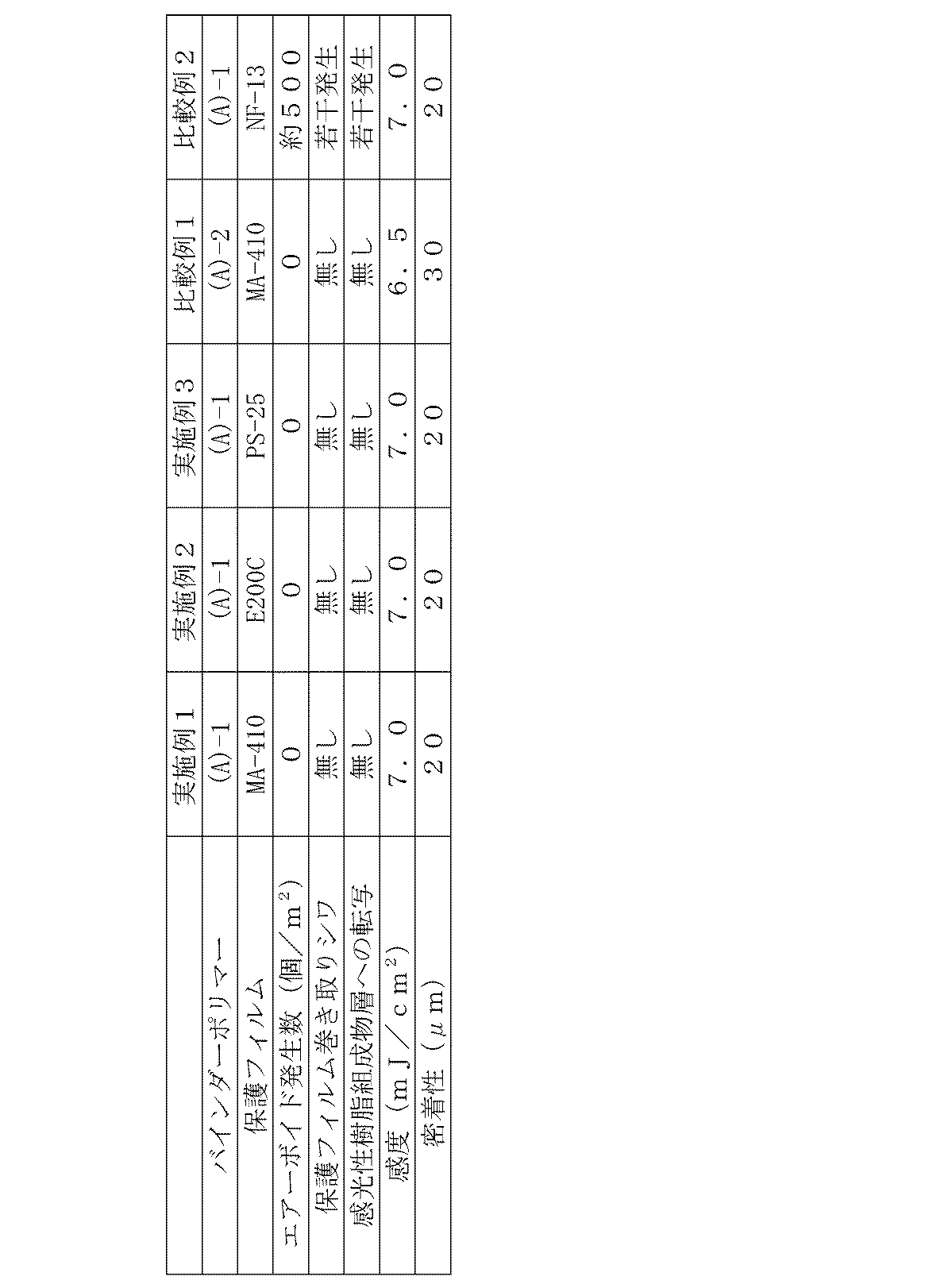
次いで、得られた感光性樹脂組成物(実施例1〜実施例3、並びに、比較例1及び比較例2)の溶液を、16μm厚のポリエチレンテレフタレートフィルム(ヘーズ:1.7%、商品名GS−16,帝人社製)上に均一に塗布し、100℃の熱風対流式乾燥機で10分間乾燥した後、Ra1、Rmax1,Ra2及びRmax2の値が既知のポリエチレン製保護フィルム(フィルム長手方向の引張強さ:16Mpa、フィルム幅方向の引張強さ:12Mpa、商品名:NF−15,タマポリ社製)で保護し感光性エレメント(実施例1〜実施例3、並びに、比較例1及び比較例2)を得た。各感光性エレメントの感光性樹脂組成物層の乾燥後の膜厚は、それぞれ30μmであった。
【0104】
なお、使用した保護フィルムのRa1、Rmax1,Ra2及びRmax2の値を後述の表2に示す。また、表2中、「MA-410」とは、王子製紙社製、ポリプロピレンフィルムを示し、「E-200C」とは、王子製紙社製、ポリプロピレンフィルムを示し、「PS-25」とは、帝人社製ポリエチレンテレフタレートフィルムを示し、「NF-13」とは、タマポリ社製、ポリエチレンフィルムを示す。
【0105】
次に、UV分光計(社日立製作所製228A型Wビーム分光光度計)を用いて、各感光性エレメント(実施例1〜実施例3、並びに、比較例1及び比較例2)の感光性樹脂組成物層の波長365nmの紫外線に対する透過率を測定した。透過率は、まず測定側に支持フィルム及び感光性樹脂組成物層からなる各感光性エレメントを置き、リファレンス側に支持フィルムを置き、T%(パーセント透過率)モードにより700〜300μmまでを連続測定し、365nmの値を読みとることにより測定した。その結果を後述の表3に示す。
【0106】
一方、厚さ0.15mm厚、20cm角の銅合金(ヤマハオーリンメタル社製、商品名:C−7025)を3質量%水酸化ナトリウム水溶液、50℃に1分間浸漬し、次いで1体積質量%塩酸水溶液、25℃に、1分間浸漬し、その後水洗、乾燥し、得られた基板上に各感光性エレメント(実施例1〜実施例3、並びに、比較例1及び比較例2)の保護フィルムを除去しながら、ロール温度:110℃、圧力:0.39MPa、速度:2m/分でラミネートした。次いで、このようにして得られた基板を、3KWの超高圧水銀灯(社オーク製作所製、HMW−201GX)で70mJ/cm2の露光を行った。
【0107】
露光後の各基板上のエアーボイド数を100倍の光学顕微鏡を用いて測定した。また、各支持フィルムのフィッシュアイの大きさ及び数を100倍の光学顕微鏡を用いて測定した。その結果を後述の表2に示す。
【0108】
一方、銅箔(厚み35μm)を両面に積層したガラスエポキシ材である銅張り積層板(日立化成工業社製、商品名MCL−E−61)の銅表面を、#600相当のブラシを持つ研磨機(三啓社製)を用いて研磨し、水洗後、空気流で乾燥し、得られた銅張り積層板を80℃に加温し、その銅表面上に各感光性樹脂組成物層(実施例1〜実施例3、並びに、比較例1及び比較例2の各感光性樹脂組成物層)を保護フィルムを剥がしながら120℃のヒートロールを用い3m/分の速度でラミネートした。
【0109】
次に、高圧水銀灯ランプを有する露光機(オーク社製)HMW−201Bを用いて、ネガとしてストーファー21段ステップタブレットを試験片の上に置いて、70mJ/cm2で露光した。
【0110】
次に、ポリエチレンテレフタレートフィルムを剥離し、30℃で1質量%炭酸ナトリウム水溶液を40秒間スプレーし、未露光部分を除去した後、銅張り積層板上に形成された光硬化膜のステップタブレットの段数を測定することにより、感光性樹脂組成物の光感度を評価した。その結果を後述の表3に示す。光感度は、ステップタブレットの段数で示され、このステップタブレットの段数が高いほど、光感度が高いことを示す。
【0111】
また、密着性は、ストーファーの21段ステップタブレットを有するフォトツールと解像度評価用ネガとしてライン幅/スペース幅が10/400〜50/400(単位:μm)の配線パターンを有するフォトツールを密着させ、ストーファーの21段ステップタブレットの現像後の残存ステップ段数が7.0となるエネルギー量で露光を行った。ここで、密着性は、現像処理によって剥離せずに密着しているライン幅の最も小さい値により評価した。密着性の評価は数値が小さいほど良好な値でることを示す。その結果を表3に示す。
【0112】
【表2】
【表3】
表3に示した結果から明らかなように、実施例1及び実施例2のは、エアーボイド、ラミネートシワ、感光性樹脂組成物層への転写がなく、かつ密着性も良好であることが確認された。
【0115】
【発明の効果】
以上説明したように、本発明によれば、プリント配線板の製造時において、エアーボイドの発生を充分に防止可能な感光性樹脂組成物層を有する感光性エレメントを提供することが可能となる。また、本発明によれば、かかる感光性エレメントを用いたレジストパターンの形成方法及びプリント配線板の製造方法を提供することが可能となる。[0001]
TECHNICAL FIELD OF THE INVENTION
The present invention relates to a photosensitive element, a method for forming a resist pattern using the same, and a method for manufacturing a printed wiring board.
[0002]
[Prior art]
In the field of manufacturing printed wiring boards, a photosensitive resin composition or a layer made of the photosensitive resin composition (hereinafter, referred to as a “photosensitive resin composition layer”) is used as a resist material used for etching, plating, and the like. 2. Description of the Related Art Photosensitive elements (laminates) formed on a support film and having a structure in which a protective film is disposed on a photosensitive resin composition layer are widely used.
[0003]
Conventionally, a printed wiring board has been manufactured using the photosensitive element according to, for example, the following procedure. That is, first, the photosensitive resin composition layer of the photosensitive element is laminated on a circuit-forming substrate such as a copper-clad laminate. At this time, the surface of the photosensitive resin composition layer opposite to the surface in contact with the support film (hereinafter referred to as the “lower surface” of the photosensitive resin composition layer) (hereinafter, the “upper surface of the photosensitive resin composition layer”) ") Is in close contact with the surface of the circuit forming substrate on which the circuit is to be formed. Therefore, when the protective film is disposed on the upper surface of the photosensitive resin composition layer, this laminating operation is performed while removing the protective film. Next, the photosensitive resin composition layer is heat-pressed to the underlying circuit-forming substrate (normal pressure lamination method).
[0004]
Next, pattern exposure is performed through a mask film or the like. At this time, the support film is peeled at any timing before or after exposure. Thereafter, the unexposed portions are dissolved or dispersed and removed with a developer. Next, an etching or plating process is performed to form a pattern, and finally, a cured portion is peeled and removed.
[0005]
Here, the etching method is a method in which a metal surface that is not covered with a cured resist formed after development is removed by etching, and then the resist is removed. On the other hand, the plating method is a method in which a metal surface not covered with a cured resist formed after development is subjected to a plating treatment such as copper and solder, and then the resist is removed and the metal surface covered with the resist is etched. .
[0006]
As a support film for the photosensitive element, a polyester film such as polyethylene terephthalate has conventionally been used. Further, as the protective film, a polyolefin film such as a polyethylene film has been conventionally used. The polyolefin film used as a protective film is usually produced by hot-melting a raw material, kneading, extruding, biaxially stretching, casting or inflation.
[0007]
In recent years, as the trend of lighter, thinner and smaller semiconductor devices and the variety of products in small quantities has progressed, so-called package substrates such as lead frames and BGAs and CSPs used for mounting IC chips on substrates have become more multi-pin and narrower. I'm advancing. The density of printed wiring boards on which these semiconductor packages are mounted is rapidly increasing.
[0008]
Therefore, the contact area between the circuit-forming substrate such as a copper-clad laminate and the patterned photosensitive resin composition layer tends to be small. For this reason, the photosensitive resin composition layer and the photosensitive element are excellent in mechanical strength, chemical resistance, flexibility, and circuit formation substrate in the development, etching or plating process during the production of a printed wiring board. In addition to the required adhesive force (adhesion), high resolution and reduction in manufacturing cost are also required. As one of the promising techniques for meeting these demands, a technique for reducing the thickness of the photosensitive resin composition layer and the photosensitive element has been proposed.
[0009]
However, if the thickness of the photosensitive element is simply reduced, the embedding property (embedding followability) of the photosensitive resin composition layer into the uneven portions existing on the surface of the circuit forming substrate is reduced. When manufacturing a printed circuit board, the etching method causes chipping and disconnection of a circuit pattern, and the plating method causes short circuit. Therefore, various studies have been made to obtain a printed wiring board by laminating a thinned photosensitive element on a circuit forming substrate while preventing the occurrence of these problems.
[0010]
As a method for manufacturing a printed wiring board using such a photosensitive element, for example, a vacuum laminating method (for example, see Patent Document 1, Patent Document 2, and Patent Document 3) different from a conventional normal pressure laminating method is used. A known manufacturing method is known.
[0011]
[Patent Document 1]
JP-B-53-31670
[Patent Document 2]
JP-B-51-63702
[Patent Document 3]
JP-A-1-314144
[0012]
[Problems to be solved by the invention]
However, in a conventional method for manufacturing a printed wiring board using a photosensitive element having a protective film, such as Patent Document 1, Patent Document 2, and Patent Document 3, thinning of a photosensitive resin composition layer (for example, (Thickness: 30 μm or less), the embedding property (embedding followability) of the photosensitive resin composition layer in the uneven portions existing on the surface of the circuit forming substrate is reduced. There is a problem that the generation of air voids cannot be sufficiently prevented.
[0013]
More specifically, the protective film constituting the photosensitive element generally contains particles of foreign matter called "fish eyes" and particles of undissolved matter and thermally degraded matter. For example, fish eye particles generally have a diameter of 10 μm to 1 mm, and the fish eye particles form projections protruding from the surface of the protective film at a height of, for example, 1 to 50 μm.
[0014]
The projections formed by the particles composed of such fish eyes, undissolved matter and thermally degraded matter cause a depression in the photosensitive resin composition layer and cause air voids to be formed on the circuit forming substrate after lamination. It becomes. That is, when a photosensitive element having a structure in which a photosensitive resin composition layer is disposed between a support film and a protective film is peeled off and laminated on a circuit forming substrate, an air void is formed.
[0015]
The air voids have a correlation with the thickness of the photosensitive resin composition layer, and are more likely to occur as the thickness of the photosensitive resin composition layer decreases. Therefore, in the process of forming a resist image of exposure and development, which is the next process of lamination, pattern chipping and disconnection occur. This phenomenon causes chipping and disconnection of the circuit pattern in the case of the etching method, and causes a short circuit in the case of the plating method.
[0016]
For example, as a measure to prevent the occurrence of the above-mentioned air voids, the fluidity of the resin of the photosensitive resin composition layer due to heat and pressure is improved, and the photosensitive resin composition layer with respect to the unevenness of the circuit forming substrate surface during lamination. There is a method for improving the embedding property. However, in this case, there is a problem that the photosensitive resin composition layer oozes out from the edge of the photosensitive element, which is called edge fusion, and the laminating property is deteriorated.
[0017]
When a printed wiring board is manufactured using a photosensitive element that cannot sufficiently prevent the occurrence of air voids, mechanical strength, chemical resistance, flexibility, adhesion to the circuit forming substrate in the development, etching, or plating process A sufficient force (adhesion) cannot be obtained, and a sufficient resolution cannot be obtained. Further, in this case, it is extremely difficult to increase the density of the printed wiring board.
[0018]
Further, a method using a film having a smooth surface as the protective film is also conceivable, but in this case, when the protective film is wound during lamination, there is a problem that wrinkles of the protective film are generated and lamination cannot be performed properly. .
[0019]
Further, in the conventional laminating method using the photosensitive element described in Patent Documents 1, 2 and 3, compared with the normal pressure laminating method, since the inside of the laminating chamber is vacuum, There is also a problem that the device is apt to occur, and a large installation space is required due to the large scale of the device.
[0020]
The present invention has been made in view of the above problems, and has an object to provide a photosensitive element having a photosensitive resin composition layer capable of sufficiently preventing the generation of air voids during the production of a printed wiring board. And Another object of the present invention is to provide a method for forming a resist pattern using the photosensitive element and a method for manufacturing a printed wiring board.
[0021]
[Means for Solving the Problems]
The present inventors have made intensive studies and as a result, constituting the photosensitive resin composition so as to contain a specific amount of a binder polymer containing a specific amount of a specific repeating unit structure, further, from the photosensitive resin composition By forming a photosensitive element using a layer and a protective film having a surface that satisfies the specific surface roughness conditions shown below, the inventors have found that the above object can be achieved, and have reached the present invention. .
[0022]
That is, the present invention is a photosensitive element having at least a support film, a protective film made of a synthetic resin, and a photosensitive resin composition layer disposed between the support film and the protective film,
A photosensitive resin composition to be a constituent material of the photosensitive resin composition layer,
(A) a binder polymer, (B) a photopolymerizable compound having at least one polymerizable ethylenically unsaturated bond, and (C) a photopolymerization initiator,
(A) The binder polymer contains at least a repeating unit based on styrene or a styrene derivative in its molecule, and
The content of the repeating unit based on styrene or a styrene derivative is 0.1 to 30% by mass based on the total mass of the molecule,
The inner surface of the protective film that is in contact with the photosensitive resin composition layer and the outer surface of the protective film that is not in contact with the photosensitive resin composition layer are represented by the following formulas (1) to (4). Are formed so as to satisfy the conditions of surface roughness at the same time,
A photosensitive element is provided.
Ra1 ≦ 0.15 μm (1)
Rmax1 ≦ 1.5 μm (2)
0.1 μm ≦ Ra2 ≦ 0.8 μm (3)
1 μm ≦ Rmax2 ≦ 5 μm (4)
[In formulas (1) to (4),
Ra1 is a parameter representing the surface roughness of the inner surface, and indicates a value of a center line average roughness (Ra) defined in JIS B 0601-1982 measured in the inner surface;
Rmax1 is a parameter representing the surface roughness of the inner surface, and indicates a value of a maximum height (Rmax) defined in JIS B 0601-1982 measured in the inner surface;
Ra2 is a parameter representing the surface roughness of the outer surface, and indicates a value of a center line average roughness (Ra) defined in JIS B 0601-1982 measured in the outer surface;
Rmax2 is a parameter representing the surface roughness of the outer surface, and indicates a value of a maximum height (Rmax) defined in JIS B 0601-1982 measured in the outer surface. ]
[0023]
The photosensitive resin composition serving as a constituent material of the photosensitive resin composition layer of the photosensitive element according to the present invention contains (A) a repeating unit based on styrene or a styrene derivative, and contains the repeating unit. By adjusting the ratio to the above-mentioned range, the fluidity with respect to heat and pressure in the photosensitive resin composition layer containing the same as a constituent material can be sufficiently embedded in the surface of the circuit-forming substrate described above (embedding follow-up). G) can be adjusted to a level that can obtain the same.
[0024]
That is, the photosensitive resin composition layer containing the above photosensitive resin composition as a constituent material has sufficient laminating properties, and if this is used for the production of a printed wiring board, it can be used when laminating a circuit forming substrate. Thus, the generation of the air voids described above can be sufficiently prevented. In addition, the occurrence of the edge fusion described above can be sufficiently prevented.
[0025]
Further, the photosensitive resin composition layer containing the photosensitive resin composition having the above-described component composition as a constituent material, during the production of a printed wiring board, during plating and etching, mechanical strength, chemical resistance, flexibility, It shows excellent properties such as adhesive strength (adhesion) to a circuit forming substrate.
[0026]
The photosensitive element of the present invention is provided with a photosensitive resin composition layer having a photosensitive resin composition having the above-described component composition as a constituent material. Applicable to production. That is, if this is used in the manufacture of a printed wiring board, the above-described generation of air voids can be sufficiently prevented during lamination on a circuit forming substrate. In addition, the occurrence of the edge fusion described above can be sufficiently prevented.
[0027]
Furthermore, the photosensitive element of the present invention is excellent in mechanical strength, chemical resistance, flexibility, adhesive strength (adhesion) to a circuit forming substrate, etc., during plating and etching in the production of a printed wiring board. Show characteristics. Therefore, the photosensitive element of the present invention enables the photosensitive resin composition layer to be laminated on the circuit-forming substrate with high yield in the production of a printed wiring board (printed circuit board). It is also useful for densification.
[0028]
Further, the present invention, the protective film of the photosensitive element of the present invention described above is gradually peeled from the photosensitive resin composition layer, simultaneously with the surface portion of the photosensitive resin composition layer gradually exposed at the same time. A first step of laminating a photosensitive resin composition layer on a circuit forming substrate by bringing the photosensitive resin composition layer into close contact with a surface of the circuit forming substrate on which a circuit is to be formed; and a predetermined portion of the photosensitive resin composition layer to be exposed. Forming a light-exposed portion by irradiating the exposed portion with an actinic ray, and then removing a portion other than the light-exposed portion.
[0029]
The present invention also provides a method for manufacturing a printed wiring board, characterized by etching or plating a circuit-forming substrate on which a resist pattern has been formed by the above-described method for forming a resist pattern of the present invention.
[0030]
The method of forming a resist pattern of the present invention and the method of manufacturing a printed wiring board of the present invention use the above-described photosensitive element of the present invention. Exposure and etching or plating become possible, and it is possible to easily realize high density of a printed wiring board (printed circuit board).
[0031]
BEST MODE FOR CARRYING OUT THE INVENTION
Hereinafter, embodiments of the present invention will be described in detail. In the present invention, (meth) acrylic acid means acrylic acid or methacrylic acid, (meth) acrylate means acrylate or methacrylate corresponding thereto, and (meth) acryloyl group means acryloyl group or methacryloyl group. means.
[0032]
(Photosensitive resin composition)
The photosensitive resin composition which is a constituent material of the photosensitive resin composition layer of the photosensitive element of the present invention has a surface roughness of the photosensitive resin composition layer represented by the following formulas (1) to (4). A photosensitive element is formed together with a protective film having a surface satisfying the conditions, and the photosensitive element has a configuration suitable for use in manufacturing a printed wiring board.
[0033]
That is, the photosensitive resin composition is a photosensitive element having at least a support film, a protective film made of a synthetic resin, and a photosensitive resin composition layer disposed between the support film and the protective film. A photosensitive resin composition serving as a constituent material of a resin composition layer, comprising: (A) a binder polymer; (B) a photopolymerizable compound having at least one polymerizable ethylenically unsaturated bond; It contains at least a photopolymerization initiator.
[0034]
If a photosensitive element having both the photosensitive resin composition layer and the protective film is used in the manufacture of a printed wiring board, the occurrence of the above-described air voids can be sufficiently prevented at the time of lamination to a circuit forming substrate. . In addition, the occurrence of the edge fusion described above can be sufficiently prevented.
[0035]
First, the binder polymer as the component (A) will be described. This binder polymer contains at least a repeating unit based on styrene or a styrene derivative in the molecule, and the content of the repeating unit based on styrene or the styrene derivative is 0.1 to 30 mass% based on the total mass of the molecule. %. Thereby, both the adhesiveness and the peeling property of the photosensitive resin composition layer containing the photosensitive resin composition as a constituent material with respect to the circuit forming substrate can be improved.
[0036]
In light of the adhesiveness and the release characteristics, the content of the repeating unit based on styrene or a styrene derivative is preferably 1% to 30% by mass, more preferably 1% to 28% by mass, and 1.5% to 30% by mass. More preferably, it is 27% by mass. When the content is less than 0.1% by mass, the adhesion is insufficient, and when the content is more than 30% by mass, the exfoliated pieces become large and the exfoliation properties such as the exfoliation time become long. Become. Further, from the viewpoint of the adhesion and the peeling property, it is preferable that the binder polymer (A) contains a repeating unit based on methacrylic acid as a constituent component.
[0037]
In the present invention, the “styrene derivative” refers to a styrene derivative in which a hydrogen atom has been substituted with a substituent (an organic group such as an alkyl group, a halogen atom, or the like).
[0038]
When a photosensitive resin composition layer is formed using this binder polymer, one type of binder polymer may be used alone, or two or more types of binder polymers may be used in any combination. When two or more binder polymers are used in combination, examples of the binder polymer include two or more binder polymers composed of different copolymer components (including different repeating units as constituent components), and two or more binder polymers having different weight average molecular weights. Polymers, two or more kinds of binder polymers having different dispersities, and the like.
[0039]
The weight average molecular weight (Mw) and the number average molecular weight (Mn) of the binder polymer can be measured by gel permeation chromatography (GPC) (converted by a calibration curve using standard polystyrene). According to this measurement method, the Mw of the binder polymer is preferably 20,000 to 300,000, and more preferably 20,000 to 100,000. When Mw is less than 20,000, the developer resistance tends to decrease, and when it exceeds 300,000, the development time tends to be long.
[0040]
The dispersity (Mw / Mn) of the binder polymer (A) is preferably from 1.0 to 6.0, and more preferably from 1.0 to 3.0. If the degree of dispersion exceeds 6.0, the adhesion and the resolution tend to decrease.
[0041]
Examples of the binder polymer (A) include an acrylic resin, a styrene resin, an epoxy resin, an amide resin, an amide epoxy resin, an alkyd resin, and a phenol resin. From the viewpoint of alkali developability, an acrylic resin is preferred. These can be used alone or in combination of two or more.
[0042]
The (A) binder polymer can be produced, for example, by radically polymerizing a polymerizable monomer. As the polymerizable monomer, for example, a polymerizable styrene derivative substituted at the α-position or an aromatic ring such as styrene, vinyltoluene, and α-methylstyrene is included as an essential copolymerization component. Other components include acrylamide such as diacetone acrylamide, esters of vinyl alcohol such as acrylonitrile and vinyl-n-butyl ether, alkyl (meth) acrylate, tetrahydrofurfuryl (meth) acrylate, and dimethyl (meth) acrylate. Aminoethyl ester, diethylaminoethyl (meth) acrylate, glycidyl (meth) acrylate, 2,2,2-trifluoroethyl (meth) acrylate, 2,2,3,3-tetrafluoropropyl (meth) acrylate , (Meth) acrylic acid, α-bromo (meth) acrylic acid, α-chloro (meth) acrylic acid, β-furyl (meth) acrylic acid, β-styryl (meth) acrylic acid, maleic acid, maleic anhydride , Monomethyl maleate, male Ynoic acid monoethyl maleate monoesters such as maleic acid monoisopropyl, fumaric acid, cinnamic acid, alpha-cyanocinnamic acid, itaconic acid, crotonic acid, propiolic acid.
[0043]
Examples of the alkyl (meth) acrylate include compounds represented by the following general formula (I), and compounds in which an alkyl group of these compounds is substituted with a hydroxyl group, an epoxy group, a halogen group, or the like. However, in the following general formula (I), R Three Represents a hydrogen atom or a methyl group; Four Represents an alkyl group having 1 to 12 carbon atoms.
[0044]
CH Two = C (R Three ) -COOR Four ... (I)
[0045]
R in the above general formula (I) Four As an alkyl group having 1 to 12 carbon atoms represented by, for example, methyl group, ethyl group, propyl group, butyl group, pentyl group, hexyl group, heptyl group, octyl group, nonyl group, decyl group, undecyl group, dodecyl And the structural isomers thereof. Examples of the monomer represented by the general formula (I) include (meth) acrylic acid methyl ester, (meth) acrylic acid ethyl ester, (meth) acrylic acid propyl ester, (meth) acrylic acid butyl ester, Pentyl (meth) acrylate, hexyl (meth) acrylate, heptyl (meth) acrylate, octyl (meth) acrylate, 2-ethylhexyl (meth) acrylate, nonyl (meth) acrylate, Examples include decyl (meth) acrylate, undecyl (meth) acrylate, and dodecyl (meth) acrylate. These can be used alone or in combination of two or more.
[0046]
It is preferable that the binder polymer (A) in the present invention is composed of one or more polymers having a carboxyl group from the viewpoint of developability when performing alkali development using an alkali solution. Such a binder polymer (A) can be produced, for example, by radically polymerizing a polymerizable monomer having a carboxyl group and another polymerizable monomer.
[0047]
(A) The binder polymer preferably has an acid value of 100 to 500 mgKOH / g, more preferably 100 to 300 mgKOH / g. When the acid value is less than 100 mgKOH / g, the developing time tends to be delayed, and when it exceeds 500 mgKOH / g, the developing solution resistance of the photocured resist tends to decrease.
[0048]
Next, the photopolymerizable compound having at least one polymerizable ethylenically unsaturated bond (hereinafter, referred to as “photopolymerizable compound”), which is the component (B), will be described.
[0049]
Examples of the photopolymerizable compound include, for example, a bisphenol A-based (meth) acrylate compound. For example, 2,2-bis (4-((meth) acryloxypolyethoxy) phenyl) propane, 2,2-bis (4-((meth) acryloxypolypropoxy) phenyl) propane, 2,2-bis ( Bisphenol A-based (meth) acrylate compounds such as 4-((meth) acryloxypolybutoxy) phenyl) propane and 2,2-bis (4-((meth) acryloxypolyethoxypolypropoxy) phenyl) propane are exemplified. Can be
[0050]
Examples of the 2,2-bis (4-((meth) acryloxypolyethoxy) phenyl) propane include, for example, 2,2-bis (4-((meth) acryloxydiethoxy) phenyl) propane, 2,2 -Bis (4-((meth) acryloxytriethoxy) phenyl) propane, 2,2-bis (4-((meth) acryloxytetraethoxy) phenyl) propane, 2,2-bis (4-((meta ) Acryloxypentaethoxy) phenyl) propane, 2,2-bis (4-((meth) acryloxyhexaethoxy) phenyl) propane, 2,2-bis (4-((meth) acryloxyheptaethoxy) phenyl) Propane, 2,2-bis (4-((meth) acryloxyoctaethoxy) phenyl) propane, 2,2-bis (4-((meth) acryloxynonae) (Xy) phenyl) propane, 2,2-bis (4-((meth) acryloxydecaethoxy) phenyl), 2,2-bis (4-((meth) acryloxyundecaethoxy) phenyl), 2,2 -Bis (4-((meth) acryloxide decaethoxy) phenyl), 2,2-bis (4-((meth) acryloxytridecaethoxy) phenyl), 2,2-bis (4-((meth) (Acryloxytetradecaethoxy) phenyl), 2,2-bis (4-((meth) acryloxypentadecaethoxy) phenyl), 2,2-bis (4-((meth) acryloxyhexadecaethoxy) phenyl) And the like, and 2,2-bis (4- (methacryloxypentaethoxy) phenyl) propane is commercially available as BPE-500 (product name, manufactured by Shin-Nakamura Chemical Co., Ltd.). , And the 2,2-bis (4- (methacryloxy pentadecanoyl) phenyl) is, BPE-1300 (manufactured by Shin Nakamura Chemical Co., Ltd., product name) is commercially available as. These are used alone or in combination of two or more.
[0051]
Examples of the 2,2-bis (4-((meth) acryloxypolypropoxy) phenyl) propane include, for example, 2,2-bis (4-((meth) acryloxydipropoxy) phenyl) propane, 2,2 -Bis (4-((meth) acryloxytripropoxy) phenyl) propane, 2,2-bis (4-((meth) acryloxytetrapropoxy) phenyl) propane, 2,2-bis (4-((meta ) Acryloxypentapropoxy) phenyl) propane, 2,2-bis (4-((meth) acryloxyhexapropoxy) phenyl) propane, 2,2-bis (4-((meth) acryloxyheptapropoxy) phenyl) Propane, 2,2-bis (4-((meth) acryloxyoctapropoxy) phenyl) propane, 2,2-bis (4-((meth) a (Riloxynonapropoxy) phenyl) propane, 2,2-bis (4-((meth) acryloxydecapropoxy) phenyl), 2,2-bis (4-((meth) acryloxyundecapropoxy) phenyl), 2,2-bis (4-((meth) acryloxydedecapropoxy) phenyl), 2,2-bis (4-((meth) acryloxytridecapropoxy) phenyl), 2,2-bis (4- ( (Meth) acryloxytetradecapropoxy) phenyl), 2,2-bis (4-((meth) acryloxypentadecapropoxy) phenyl), 2,2-bis (4-((meth) acryloxyhexadecapropoxy) ) Phenyl) and the like. These are used alone or in combination of two or more.
[0052]
Examples of the 2,2-bis (4-((meth) acryloxypolyethoxypolypropoxy) phenyl) propane include, for example, 2,2-bis (4-((meth) acryloxydiethoxyoctapropoxy) phenyl) propane And 2,2-bis (4-((meth) acryloxytetraethoxytetrapropoxy) phenyl) propane, 2,2-bis (4-((meth) acryloxyhexaethoxyhexapropoxy) phenyl) propane and the like. . These are used alone or in combination of two or more.
[0053]
Examples of the photopolymerizable compound other than the bisphenol A (meth) acrylate compound include a compound obtained by reacting an α, β-unsaturated carboxylic acid with a polyhydric alcohol, and an α, β-unsaturated compound in a glycidyl group-containing compound. A compound obtained by reacting a saturated carboxylic acid, a urethane monomer such as a (meth) acrylate compound having a urethane bond, nonylphenyldioxylene (meth) acrylate, γ-chloro-β-hydroxypropyl-β ′-(meth) acryloyl Oxyethyl-o-phthalate, β-hydroxyethyl-β ′-(meth) acryloyloxyethyl-o-phthalate, β-hydroxypropyl-β ′-(meth) acryloyloxyethyl-o-phthalate, (meth) acrylic acid Alkyl ester, EO-modified nonylphenyl (meth) acrylate And the like, but it is preferable to use together a photopolymerizable compound having one polymerizable ethylenically unsaturated bond in the molecule. These are used alone or in combination of two or more.
[0054]
Examples of the compound obtained by reacting the polyhydric alcohol with an α, β-unsaturated carboxylic acid include polyethylene glycol di (meth) acrylate having 2 to 14 ethylene groups and 2 to 14 propylene groups. 14, polypropylene glycol di (meth) acrylate, trimethylolpropanedi (meth) acrylate, trimethylolpropanetri (meth) acrylate, trimethylolpropaneethoxytri (meth) acrylate, trimethylolpropanediethoxytri (meth) acrylate, Trimethylolpropanetriethoxytri (meth) acrylate, trimethylolpropanetetraethoxytri (meth) acrylate, trimethylolpropanepentaethoxytri (meth) acrylate, tetramethylolmethanetri (meth) acrylate ) Acrylate, tetramethylolmethanetetra (meth) acrylate, polypropylene glycol di (meth) acrylate having 2 to 14 propylene groups, dipentaerythritol penta (meth) acrylate, dipentaerythritol hexa (meth) acrylate, and the like. Can be
[0055]
Examples of the α, β-unsaturated carboxylic acid include (meth) acrylic acid.
[0056]
Examples of the glycidyl group-containing compound include trimethylolpropane triglycidyl ether tri (meth) acrylate and 2,2-bis (4- (meth) acryloxy-2-hydroxy-propyloxy) phenyl.
[0057]
Examples of the urethane monomer include (meth) acrylic monomers having an OH group at the β-position and diisocyanate compounds such as isophorone diisocyanate, 2,6-toluene diisocyanate, 2,4-toluene diisocyanate, and 1,6-hexamethylene diisocyanate. And tris ((meth) acryloxytetraethylene glycol isocyanate) hexamethylene isocyanurate, EO-modified urethane di (meth) acrylate, and EO, PO-modified urethane di (meth) acrylate. EO represents ethylene oxide, and the EO-modified compound has a block structure of an ethylene oxide group. PO represents propylene oxide, and the PO-modified compound has a block structure of a propylene oxide group. Examples of the EO-modified urethane di (meth) acrylate include UA-11 manufactured by Shin-Nakamura Chemical Co., Ltd. Examples of the EO, PO-modified urethane di (meth) acrylate include UA-13 manufactured by Shin-Nakamura Chemical Co., Ltd., and the like.
[0058]
Examples of the alkyl (meth) acrylate include methyl (meth) acrylate, ethyl (meth) acrylate, butyl (meth) acrylate, 2-ethylhexyl (meth) acrylate, and the like. .
[0059]
Next, the photopolymerization initiator as the component (C) will be described. As the photopolymerization initiator of the component (C) in the present invention, for example, benzophenone, N, N'-tetramethyl-4,4'-diaminobenzophenone (Michler's ketone), N, N'-tetraethyl-4,4'- Diaminobenzophenone, 4-methoxy-4'-dimethylaminobenzophenone, 2-benzyl-2-dimethylamino-1- (4-morpholinophenyl) -butanone-1,2-methyl-1- [4- (methylthio) phenyl] Aromatic ketones such as -2-morpholino-propanone-1, 2-ethylanthraquinone, phenanthrenequinone, 2-tert-butylanthraquinone, octamethylanthraquinone, 1,2-benzanthraquinone, 2,3-benzanthraquinone, and 2-phenyl Anthraquinone, 2,3-diphenylanthraquinone, 1- Quinones such as loloanthraquinone, 2-methylanthraquinone, 1,4-naphthoquinone, 9,10-phenantaraquinone, 2-methyl-1,4-naphthoquinone, and 2,3-dimethylanthraquinone; benzoin methyl ether; benzoin ethyl ether; Benzoin ether compounds such as benzoin phenyl ether; benzoin compounds such as benzoin, methyl benzoin and ethyl benzoin; benzyl derivatives such as benzyl dimethyl ketal; 2- (o-chlorophenyl) -4,5-diphenylimidazole dimer; o-chlorophenyl) -4,5-di (methoxyphenyl) imidazole dimer, 2- (o-fluorophenyl) -4,5-diphenylimidazole dimer, 2- (o-methoxyphenyl) -4,5 -Diphenylimidazole Dimer, 2,4,5-triarylimidazole dimer such as 2- (p-methoxyphenyl) -4,5-diphenylimidazole dimer, 9-phenylacridine, 1,7-bis (9, Acridine derivatives such as 9'-acridinyl) heptane; N-phenylglycine; N-phenylglycine derivatives; coumarin compounds;
[0060]
Further, the substituents of the aryl groups of the two 2,4,5-triarylimidazoles may be the same to give a target compound, or different asymmetric compounds may be given. Further, a thioxanthone compound and a tertiary amine compound may be combined, such as a combination of diethylthioxanthone and dimethylaminobenzoic acid. From the viewpoints of adhesion and sensitivity, 2,4,5-triarylimidazole dimer is more preferable. These are used alone or in combination of two or more.
[0061]
Here, the amount of the binder polymer (A) described above is preferably 40 to 80 parts by mass, preferably 45 to 70 parts by mass, based on 100 parts by mass of the total of the components (A) and (B). More preferably, it is a part. If the compounding amount is less than 40 parts by mass, the photocured product tends to become brittle, and when used as a photosensitive element, the coating properties tend to be poor, and if it exceeds 80 parts by mass, the photosensitivity tends to be insufficient. is there.
[0062]
Further, the blending amount of the (B) photopolymerizable compound is preferably 20 to 60 parts by mass, and more preferably 30 to 55 parts by mass with respect to 100 parts by mass of the total of the components (A) and (B). Is more preferable. If the amount is less than 20 parts by mass, the photosensitivity tends to be insufficient, and if it exceeds 60 parts by mass, the photocured product tends to be brittle.
[0063]
The compounding amount of the photopolymerization initiator (C) is preferably 0.1 to 20 parts by mass, and preferably 0.2 to 10 parts by mass based on 100 parts by mass of the total of the components (A) and (B). Is more preferable. When the amount is less than 0.1 part by mass, the photosensitivity tends to be insufficient. When the amount is more than 20 parts by mass, the absorption on the surface of the composition during exposure increases, and the internal light curing is insufficient. It tends to be.
[0064]
Further, the photosensitive resin composition of the present invention may contain, if necessary, a dye such as malachite green, a photochromic agent such as tribromophenylsulfone or leucocrystal violet, a thermochromic inhibitor, a p-toluenesulfonamide or the like. Plasticizer, pigment, filler, defoamer, flame retardant, stabilizer, adhesion promoter, leveling agent, peeling accelerator, antioxidant, fragrance, imaging agent, thermal crosslinking agent, etc. Each component (B) can be contained in an amount of about 0.01 to 20 parts by mass based on 100 parts by mass of the total amount of the component. These are used alone or in combination of two or more.
[0065]
Further, the photosensitive resin composition of the present invention is dissolved in a solvent such as methanol, ethanol, acetone, methyl ethyl ketone, methyl cellosolve, ethyl cellosolve, toluene, N, N-dimethylformamide, propylene glycol monomethyl ether or a mixed solvent thereof. And a solution having a solid content of about 30 to 60% by mass. This solution can be used as a coating solution for forming a photosensitive resin composition layer of a photosensitive element.
[0066]
Further, the above coating liquid may be used to form a photosensitive resin composition layer of the photosensitive element by coating and drying on a support film described below, for example, the surface of a metal plate, for example, Copper, copper-based alloy, nickel, chromium, iron, iron-based alloys such as stainless steel, preferably copper, copper-based alloy, on the surface of the iron-based alloy, applied as a liquid resist and dried, then coated with a protective film May be used.
[0067]
(Photosensitive element)
Next, the photosensitive element of the present invention will be described. The photosensitive element of the present invention has at least a support film, a protective film made of a synthetic resin, and a photosensitive resin composition layer disposed between the support film and the protective film. The photosensitive resin composition layer of the photosensitive element of the present invention has at least the components (A), (B) and (C) described above, and has the structure of the component (A) described above. A photosensitive resin composition that satisfies the content condition is contained as a constituent material. Furthermore, in the photosensitive element of the present invention, the inner surface of the protective film that is in contact with the photosensitive resin composition layer and the outer surface of the protective film that is not in contact with the photosensitive resin composition layer are represented by the following formula ( They are formed so as to simultaneously satisfy the surface roughness conditions represented by 1) to (4).
[0068]
Ra1 ≦ 0.15 μm (1)
Rmax1 ≦ 1.5 μm (2)
0.1 μm ≦ Ra2 ≦ 0.8 μm (3)
1 μm ≦ Rmax2 ≦ 5 μm (4)
[0069]
Here, in the formulas (1) to (4), Ra1 is a parameter representing the surface roughness of the inner surface, and the center line average roughness (Ra) defined in JIS B 0601-1982 measured on the inner surface. ), Rmax1 is a parameter representing the surface roughness of the inner surface, and indicates a value of the maximum height (Rmax) defined in JIS B 0601-1982 measured in the inner surface, and Ra2 is A parameter representing the surface roughness of the outer surface, which indicates the value of the center line average roughness (Ra) defined in JIS B 0601-1982 measured in the outer surface, and Rmax2 indicates the surface roughness of the outer surface. This is a parameter that indicates the value of the maximum height (Rmax) defined in JIS B 0601-1982 measured on the outer surface. The cut-off value is 0.08 mm and the measurement length is 2.5 mm.
[0070]
Here, when Ra1 exceeds 0.15 μm and Rmax1 exceeds 1.5 μm, the surface shape of the protective film is transferred to the photosensitive resin composition layer side, and the photosensitive resin composition layer is depressed. It causes air voids during lamination. Further, when Ra2 is less than 0.1 and Rmax2 is less than 1.0 μm, wrinkles occur when the protective film is wound during lamination, and the lamination operation cannot be performed smoothly. Further, when Ra2 exceeds 0.8 μm and Rmax2 exceeds 5.0 μm, when the photosensitive element is coated (when the photosensitive element is formed using the coating solution of the photosensitive resin composition) and when the slit is formed. Due to the winding tension, the surface shape of the outer surface of the protective film is transferred to the photosensitive resin composition layer, which causes air voids during the above-described lamination.
[0071]
From the same viewpoint as the above, Ra1 is preferably 0.01 to 0.1 μm. Further, Rmax1 is preferably 0.1 to 1.0 μm or less. Ra2 is preferably 0.15 to 0.4 μm. Furthermore, it is preferable that Rmax2 is 1.5 to 3.0 μm.
[0072]
As the protective film that satisfies the above condition of the surface roughness, for example, a polymer film having heat resistance and solvent resistance such as polyethylene terephthalate, polypropylene, polyethylene, and polyester can be used. Examples of commercially available products include polypropylene films such as Oji Paper's Alphan MA-410 and E-200C, manufactured by Shin-Etsu Film Co., Ltd., and polyethylene terephthalate films such as PS series such as Teijin's PS-25. It is not limited to this. As a method for adjusting the inner surface and the outer surface so as to satisfy the surface roughness condition, for example, a surface treatment such as sandblasting may be mentioned. Thereby, a protective film having an inner surface and an outer surface satisfying the above condition of the surface roughness can be easily manufactured.
[0073]
The protective film preferably has a thickness of 1 to 100 μm, more preferably 5 to 50 μm, further preferably 5 to 30 μm, and particularly preferably 15 to 30 μm. If the thickness is less than 1 μm, the protective film tends to be broken during lamination, and if it exceeds 100 μm, the cost tends to be poor.
[0074]
The number (number density) of fish eyes having a diameter of 80 μm or more contained in the protective film is 5 / m Two It is desirable that: In addition, fish eyes are materials that are heated, melted, kneaded, extruded, biaxially stretched, when a film is produced by a casting method, etc., foreign matter, undissolved matter, oxidized degraded matter, etc. of the material are taken into the film. It is a thing.
[0075]
A protective film in which the number (number density) of fish eyes satisfies the above conditions can be manufactured by selecting a material, optimizing a kneading method, filtering after melting the material, and the like. The size of the fish eye diameter varies depending on the material, but is about 10 μm to 1 mm, and the height from the surface of the protective film is about 1 μm to 50 μm. Here, the method of measuring the size of the fish eye can be measured using, for example, an optical microscope, a contact type surface roughness meter, a non-contact type surface measuring device using a laser beam, or a scanning electron microscope. In addition, the diameter of a fish eye means the maximum diameter of a fish eye.
[0076]
When the shape of the protective film (the shape of the inner surface and the outer surface) is rectangular, the tensile strength of the protective film in the longitudinal direction (the longitudinal direction of the rectangular inner surface and the outer surface) is preferably 13 MPa or more, It is preferable that the tensile strength of the protective film in the short direction (the short direction of the rectangular inner surface and the outer surface) is 9 MPa or more.
[0077]
The photosensitive resin composition layer is prepared by dissolving the photosensitive resin composition of the present invention in the solvent described above to obtain a solution (coating solution) having a solid content of about 30 to 60% by weight, and then applying the solution (coating solution). Liquid) is preferably applied to a support film and dried. The coating can be performed by a known method such as a roll coater, a comma coater, a gravure coater, an air knife coater, a die coater, and a bar coater, and the drying can be performed at 70 to 150 ° C. for about 5 to 30 minutes. In addition, the amount of the residual organic solvent in the photosensitive resin composition is preferably 2% by weight or less from the viewpoint of preventing the diffusion of the organic solvent in a later step.
[0078]
The thickness of the photosensitive resin composition layer varies depending on the application, but is preferably from 1 to 100 μm, more preferably from 1 to 50 μm as a thickness after drying. If the thickness is less than 1 μm, coating tends to be difficult industrially, and if it exceeds 100 μm, the effect of the present invention tends to be small, and the adhesive strength and the resolution tend to be reduced.
[0079]
The transmittance of the photosensitive resin composition layer to ultraviolet rays having a wavelength of 365 nm is preferably 5 to 75%, more preferably 7 to 60%, and particularly preferably 10 to 40%. If the transmittance is less than 5%, the adhesion tends to be poor, and if it exceeds 75%, the resolution tends to be poor. The transmittance can be measured by a UV spectrometer. Examples of the UV spectrometer include a 228A W-beam spectrophotometer manufactured by Hitachi, Ltd.
[0080]
As the support film, for example, a polymer film having heat resistance and solvent resistance such as polyethylene terephthalate, polypropylene, polyethylene, and polyester can be used. Further, the support film preferably has a thickness of 5 to 25 μm, more preferably 8 to 20 μm, and particularly preferably 10 to 16 μm. If the thickness is less than 5 μm, the support film tends to be broken when the support film is peeled off before development, and if it exceeds 25 μm, the resolution tends to decrease.
[0081]
Further, the haze of the support film is preferably from 0.001 to 5.0, more preferably from 0.001 to 2.0, and particularly preferably from 0.01 to 1.8. If the haze exceeds 2.0, the resolution tends to decrease. The haze is measured in accordance with JIS K 7105, and can be measured with a commercially available turbidity meter such as NDH-1001DP (manufactured by Nippon Denshoku Industries Co., Ltd.).
[0082]
In addition, since these support film and protective film must be removable from the photosensitive resin composition layer later, they must not have been subjected to a surface treatment that makes removal impossible. There is no limitation, and processing may be performed as needed. Further, these support films and protective films may be subjected to antistatic treatment as required. The protective film is adjusted so as to satisfy the above-described conditions of the surface roughness of the formulas (1) to (4) even when such a treatment is performed.
[0083]
The photosensitive element of the present invention may further have an intermediate layer such as a cushion layer, an adhesive layer, a light absorbing layer, and a gas barrier layer. The obtained photosensitive element can be stored in a sheet form or wound up in a roll form around a core.
[0084]
(Method of forming resist pattern)
Next, a method for forming a resist pattern according to the present invention will be described. The method of forming a resist pattern according to the present invention is such that the protective film of the photosensitive element of the present invention is gradually peeled off from the photosensitive resin composition layer, and the photosensitive resin composition layer gradually exposed at the same time. A first step of laminating the photosensitive resin composition layer on the circuit formation substrate by bringing the surface portion into close contact with the surface of the circuit formation substrate on which the circuit is to be formed; and exposing the photosensitive resin composition layer to light. A second step of irradiating a predetermined portion to be exposed with actinic rays to form an exposed portion, and then removing a portion other than the exposed portion. Note that the “circuit formation substrate” refers to a substrate including an insulating layer and a conductor layer formed over the insulating layer.
[0085]
As a method of laminating the photosensitive resin composition layer on the circuit forming substrate in the first step, the photosensitive resin composition layer is formed by removing the protective film and heating the photosensitive resin composition layer while forming the circuit. There is a method of laminating by pressing the substrate. Note that, in this operation, it is preferable to perform lamination under reduced pressure from the viewpoint of adhesion and followability. The lamination of the photosensitive elements is preferably performed by heating the photosensitive resin composition layer and / or the substrate for circuit formation to 70 to 130 ° C., and the pressing pressure is about 0.1 to 1.0 MPa (1 to 10 kgf / cm). Two ), But these conditions are not particularly limited. In addition, if the photosensitive resin composition layer is heated to 70 to 130 ° C. as described above, it is not necessary to pre-heat the circuit forming substrate in advance. Preheating of the substrate can also be performed.
[0086]
As a method of forming the exposed portion in the second step, there is a method of irradiating an image with an actinic ray through a negative or positive mask pattern called an artwork. At this time, when the support film present on the photosensitive resin composition layer is transparent to actinic light, the actinic light can be irradiated through the support film, and when the support film is light-shielding, After the support film is removed, the photosensitive resin composition layer is irradiated with actinic rays.
[0087]
As a light source of the actinic ray, a known light source, for example, a carbon arc lamp, a mercury vapor arc lamp, an ultra-high pressure mercury lamp, a high pressure mercury lamp, a xenon lamp, or the like that effectively emits ultraviolet rays is used. In addition, those which emit visible light effectively, such as a flood light bulb for photography and a sun lamp, are used.
[0088]
Next, as a method of removing portions other than the exposed portions after exposure, first, if a support film is present on the photosensitive resin composition layer, the support film is removed, and then wet development and dry development are performed. There is a method of removing portions other than the exposed portions by development and developing. As a result, a resist pattern is formed.
[0089]
For example, in the case of wet development, using a developing solution corresponding to a photosensitive resin composition such as an alkaline aqueous solution, an aqueous developing solution, and an organic solvent developing solution, for example, spraying, rocking immersion, brushing, scraping, etc. Develop by a known method.
[0090]
As the developing solution, a safe and stable one having good operability, such as an alkaline aqueous solution, is used. As the base of the alkaline aqueous solution, for example, alkali hydroxides such as lithium, sodium or potassium hydroxide, alkali carbonates such as lithium, sodium, potassium or ammonium carbonate or bicarbonate, potassium phosphate, phosphoric acid Alkali metal phosphates such as sodium and alkali metal pyrophosphates such as sodium pyrophosphate and potassium pyrophosphate are used.
[0091]
Examples of the alkaline aqueous solution used for development include a dilute solution of 0.1 to 5% by mass of sodium carbonate, a dilute solution of 0.1 to 5% by mass of potassium carbonate, a dilute solution of 0.1 to 5% by mass of sodium hydroxide, A dilute solution of 0.1 to 5% by mass of sodium tetraborate is preferred. The pH of the alkaline aqueous solution used for development is preferably in the range of 9 to 11, and the temperature is adjusted according to the developability of the photosensitive resin composition layer. Further, a surfactant, an antifoaming agent, a small amount of an organic solvent for promoting development, and the like may be mixed in the alkaline aqueous solution.
[0092]
Examples of the aqueous developer include a developer comprising water or an aqueous alkaline solution and one or more organic solvents. Here, as the base of the alkaline aqueous solution, other than the above-mentioned substances, for example, borax, sodium metasilicate, tetramethylammonium hydroxide, ethanolamine, ethylenediamine, diethylenetriamine, 2-amino-2-hydroxymethyl-1,3 -Propanediol, 1,3-diaminopropanol-2, morpholine and the like. The pH of the developing solution is preferably as low as possible within a range where the development of the resist can be sufficiently performed, and is preferably from 8 to 12, more preferably from 9 to 10.
[0093]
Examples of the organic solvent include triacetone alcohol, acetone, ethyl acetate, alkoxyethanol having an alkoxy group having 1 to 4 carbon atoms, ethyl alcohol, isopropyl alcohol, butyl alcohol, diethylene glycol monomethyl ether, diethylene glycol monoethyl ether, diethylene glycol monoethyl ether. Butyl ether and the like. These are used alone or in combination of two or more. The concentration of the organic solvent is usually preferably from 2 to 90% by mass, and the temperature can be adjusted according to the developing property. Further, a small amount of a surfactant, an antifoaming agent or the like can be mixed in the aqueous developer. Examples of the organic solvent-based developer used alone include 1,1,1-trichloroethane, N-methylpyrrolidone, N, N-dimethylformamide, cyclohexanone, methyl isobutyl ketone, γ-butyrolactone, and the like.
[0094]
It is preferable to add water to these organic solvents in a range of 1 to 20% by mass to prevent ignition. If necessary, two or more developing methods may be used in combination. Development methods include a dip method, a battle method, a spray method, brushing, and slapping, and a high-pressure spray method is most suitable for improving resolution.
[0095]
In addition, as processing after development, heating at about 60 to 250 ° C. or 0.2 to 10 mJ / cm Two The resist pattern may be further cured by performing light exposure to a certain degree before use.
[0096]
(Method of manufacturing printed wiring boards)
Next, a method for manufacturing a printed wiring board of the present invention will be described. In the method for manufacturing a printed wiring board according to the present invention, the circuit-forming substrate on which the resist pattern is formed is etched or plated by the above-described method for forming a resist pattern according to the present invention.
[0097]
The etching and plating of the circuit forming substrate are performed on the conductor layer and the like of the circuit forming substrate using the formed resist pattern as a mask. Examples of the etching solution for performing the etching include a cupric chloride solution, a ferric chloride solution, an alkali etching solution, and a hydrogen peroxide etching solution. Preferably, an iron solution is used. Examples of the plating method for plating include copper plating such as copper sulfate plating and copper pyrophosphate plating, solder plating such as high-throw solder plating, Watt bath (nickel sulfate-nickel chloride) plating, nickel sulfamate and the like. Gold plating such as nickel plating, hard gold plating, and soft gold plating.
[0098]
After the completion of the etching or plating, the resist pattern can be peeled off, for example, with a more alkaline aqueous solution than the alkaline aqueous solution used for development. As the strong alkaline aqueous solution, for example, a 1 to 10% by weight aqueous solution of sodium hydroxide, a 1 to 10% by weight aqueous solution of potassium hydroxide or the like is used. Examples of the peeling method include an immersion method and a spray method. The immersion method and the spray method may be used alone or in combination. Further, the printed wiring board on which the resist pattern is formed may be a multilayer printed wiring board.
[0099]
Although a printed wiring board is obtained by the above, in the method for manufacturing a printed wiring board of the present invention, since the above-described photosensitive element of the present invention is used, even when the pattern interval is narrowed, good exposure is obtained. In addition, etching or plating becomes possible, and high density can be realized.
[0100]
【Example】
Hereinafter, preferred embodiments of the present invention will be described in more detail, but the present invention is not limited to these embodiments.
[0101]
First, the components shown in Table 1 were blended to obtain solutions of the photosensitive resin compositions of Examples 1 to 3 and Comparative Examples 1 and 2. As the component (B) in Table 1, 2,2-bis (4- (methacryloxypentaethoxy) phenyl) propane was a commercially available product (manufactured by Shin-Nakamura Chemical Co., Ltd.).
[0102]
[Table 1]
Next, a solution of the obtained photosensitive resin composition (Examples 1 to 3, and Comparative Examples 1 and 2) was applied to a 16 μm-thick polyethylene terephthalate film (haze: 1.7%, trade name: GS) -16, manufactured by Teijin Limited) and dried with a hot air convection dryer at 100 ° C. for 10 minutes, and then a polyethylene protective film having a known value of Ra1, Rmax1, Ra2 and Rmax2 (film longitudinal direction). Tensile strength: 16 Mpa, tensile strength in the film width direction: 12 Mpa, trade name: NF-15, manufactured by Tamapoly Co., Ltd., protected with a photosensitive element (Examples 1 to 3, and Comparative Examples 1 and 2) 2) was obtained. The thickness of the photosensitive resin composition layer of each photosensitive element after drying was 30 μm.
[0104]
The values of Ra1, Rmax1, Ra2, and Rmax2 of the used protective film are shown in Table 2 below. In Table 2, “MA-410” indicates a polypropylene film manufactured by Oji Paper Co., Ltd., “E-200C” indicates a polypropylene film manufactured by Oji Paper Co., Ltd., and “PS-25” indicates This indicates a polyethylene terephthalate film manufactured by Teijin Limited, and “NF-13” indicates a polyethylene film manufactured by Tamapoli.
[0105]
Next, the photosensitive resin of each photosensitive element (Examples 1 to 3, and Comparative Examples 1 and 2) was measured using a UV spectrometer (Model 228A W-beam spectrophotometer manufactured by Hitachi, Ltd.). The transmittance of the composition layer to ultraviolet light having a wavelength of 365 nm was measured. The transmittance is measured by first placing each photosensitive element composed of a support film and a photosensitive resin composition layer on the measurement side, placing the support film on the reference side, and continuously measuring from 700 to 300 μm in T% (percent transmittance) mode. It was measured by reading the value at 365 nm. The results are shown in Table 3 below.
[0106]
On the other hand, a copper alloy (manufactured by Yamaha Ohlin Metal Co., Ltd., trade name: C-7025) having a thickness of 0.15 mm and a thickness of 20 cm is immersed in a 3% by mass aqueous sodium hydroxide solution at 50 ° C. for 1 minute, and then 1% by volume. A protective film of each photosensitive element (Examples 1 to 3, and Comparative Examples 1 and 2) was immersed in an aqueous hydrochloric acid solution at 25 ° C. for 1 minute, washed with water, and dried. , While laminating at a roll temperature of 110 ° C., a pressure of 0.39 MPa, and a speed of 2 m / min. Then, the substrate thus obtained was subjected to 70 mJ / cm using a 3 KW ultrahigh pressure mercury lamp (manufactured by Oak Manufacturing Co., Ltd., HMW-201GX). Two Was exposed.
[0107]
The number of air voids on each substrate after exposure was measured using a 100-fold optical microscope. In addition, the size and number of fish eyes of each support film were measured using a 100-fold optical microscope. The results are shown in Table 2 below.
[0108]
On the other hand, the copper surface of a copper-clad laminate (manufactured by Hitachi Chemical Co., Ltd., trade name: MCL-E-61), which is a glass epoxy material having copper foil (thickness: 35 μm) laminated on both sides, is polished with a brush equivalent to # 600. After being polished using a machine (manufactured by Sankeisha), washed with water, and dried in an air stream, the obtained copper-clad laminate was heated to 80 ° C., and each photosensitive resin composition layer ( The photosensitive resin composition layers of Examples 1 to 3 and Comparative Examples 1 and 2 were laminated at a speed of 3 m / min using a heat roll at 120 ° C. while peeling off the protective film.
[0109]
Next, using an exposure machine (manufactured by Oak Co.) HMW-201B having a high-pressure mercury lamp, a 21-step stofer step tablet was placed on the test piece as a negative, and 70 mJ / cm. Two Exposure.
[0110]
Next, the polyethylene terephthalate film was peeled off, and a 1% by mass aqueous solution of sodium carbonate was sprayed at 30 ° C. for 40 seconds to remove unexposed portions. Then, the number of steps of the step tablet of the photocured film formed on the copper-clad laminate was measured. Was measured to evaluate the light sensitivity of the photosensitive resin composition. The results are shown in Table 3 below. The light sensitivity is indicated by the number of steps of the step tablet. The higher the number of steps of the step tablet, the higher the light sensitivity.
[0111]
The adhesion between a phototool having a 21-step step tablet of a stofer and a phototool having a wiring pattern with a line width / space width of 10/400 to 50/400 (unit: μm) as a negative for resolution evaluation was closely adhered. Exposure was performed with an energy amount such that the number of remaining steps after development of the 21-step tablet of the stofer was 7.0. Here, the adhesion was evaluated based on the smallest value of the line width in which the line was adhered without being separated by the developing treatment. The evaluation of adhesion indicates that the smaller the numerical value, the better the value. Table 3 shows the results.
[0112]
[Table 2]
[Table 3]
As is clear from the results shown in Table 3, it was confirmed that Examples 1 and 2 had no air voids, lamination wrinkles, transfer to the photosensitive resin composition layer, and had good adhesion. Was done.
[0115]
【The invention's effect】
As described above, according to the present invention, it is possible to provide a photosensitive element having a photosensitive resin composition layer capable of sufficiently preventing the generation of air voids at the time of manufacturing a printed wiring board. Further, according to the present invention, it is possible to provide a method for forming a resist pattern using such a photosensitive element and a method for manufacturing a printed wiring board.
Claims (3)
前記感光性樹脂組成物層の構成材料となる感光性樹脂組成物が、
(A)バインダーポリマーと、(B)少なくとも1つの重合可能なエチレン性不飽和結合を有する光重合性化合物と、(C)光重合開始剤とを少なくともを含有しており、
前記(A)バインダーポリマーは、その分子内にスチレン又はスチレン誘導体に基づく繰り返し単位を少なくとも含有しており、かつ、
前記スチレン又はスチレン誘導体に基づく繰り返し単位の含有率が、分子全質量を基準として0.1〜30質量%であり、
前記保護フィルムの前記感光性樹脂組成物層に接触している内表面と、前記保護フィルムの前記感光性樹脂組成物層に接触していない外表面とが、下記式(1)〜式(4)で表される表面粗さの条件を同時に満たすようにそれぞれ形成されていること、
を特徴とする感光性エレメント。
Ra1≦0.15μm ・・・(1)
Rmax1≦1.5μm ・・・(2)
0.1μm≦Ra2≦0.8μm ・・・(3)
1μm≦Rmax2≦5μm ・・・(4)
[式(1)〜(4)中、
Ra1は、前記内表面の表面粗さを表すパラメータであって、前記内表面内において測定されるJIS B 0601-1982規定の中心線平均粗さ(Ra)の値を示し、
Rmax1は、前記内表面の表面粗さを表すパラメータであって、前記内表面内において測定されるJIS B 0601-1982規定の最大高さ(Rmax)の値を示し、
Ra2は、前記外表面の表面粗さを表すパラメータであって、前記外表面内において測定されるJIS B 0601-1982規定の中心線平均粗さ(Ra)の値を示し、
Rmax2は、前記外表面の表面粗さを表すパラメータであって、前記外表面内において測定されるJIS B 0601-1982規定の最大高さ(Rmax)の値を示す。]Support film, a protective film made of synthetic resin, a photosensitive element having at least a photosensitive resin composition layer disposed between the support film and the protective film,
A photosensitive resin composition to be a constituent material of the photosensitive resin composition layer,
(A) a binder polymer, (B) a photopolymerizable compound having at least one polymerizable ethylenically unsaturated bond, and (C) a photopolymerization initiator,
The (A) binder polymer contains at least a repeating unit based on styrene or a styrene derivative in its molecule, and
The content of the repeating unit based on the styrene or styrene derivative is 0.1 to 30% by mass based on the total mass of the molecule,
The inner surface of the protective film that is in contact with the photosensitive resin composition layer and the outer surface of the protective film that is not in contact with the photosensitive resin composition layer are represented by the following formulas (1) to (4). ) Are formed so as to simultaneously satisfy the surface roughness conditions represented by
A photosensitive element characterized by the following.
Ra1 ≦ 0.15 μm (1)
Rmax1 ≦ 1.5 μm (2)
0.1 μm ≦ Ra2 ≦ 0.8 μm (3)
1 μm ≦ Rmax2 ≦ 5 μm (4)
[In formulas (1) to (4),
Ra1 is a parameter representing the surface roughness of the inner surface, and indicates a value of a center line average roughness (Ra) defined in JIS B 0601-1982 measured in the inner surface;
Rmax1 is a parameter representing the surface roughness of the inner surface, and indicates a value of a maximum height (Rmax) defined in JIS B 0601-1982 measured in the inner surface;
Ra2 is a parameter representing the surface roughness of the outer surface, and indicates a value of a center line average roughness (Ra) defined in JIS B 0601-1982 measured in the outer surface;
Rmax2 is a parameter representing the surface roughness of the outer surface, and indicates a value of a maximum height (Rmax) defined in JIS B 0601-1982 measured in the outer surface. ]
前記感光性樹脂組成物層の露光すべき所定部分に活性光線を照射して露光部を形成させ、次いで、該露光部以外の部分を除去する第2工程と、
を少なくとも含むこと、
を特徴とするレジストパターンの形成方法。The protective film of the photosensitive element according to claim 1, wherein the protective film is gradually peeled off from the photosensitive resin composition layer. A first step of laminating the photosensitive resin composition layer on the circuit forming substrate by adhering to the surface of the forming substrate on which a circuit is to be formed;
A second step of irradiating a predetermined portion of the photosensitive resin composition layer to be exposed with actinic rays to form an exposed portion, and then removing a portion other than the exposed portion,
Including at least
A method for forming a resist pattern.
Priority Applications (1)
| Application Number | Priority Date | Filing Date | Title |
|---|---|---|---|
| JP2002359630A JP2004191648A (en) | 2002-12-11 | 2002-12-11 | Photosensitive element, method of forming resist pattern using the same, and method of manufacturing printed wiring board |
Applications Claiming Priority (1)
| Application Number | Priority Date | Filing Date | Title |
|---|---|---|---|
| JP2002359630A JP2004191648A (en) | 2002-12-11 | 2002-12-11 | Photosensitive element, method of forming resist pattern using the same, and method of manufacturing printed wiring board |
Publications (1)
| Publication Number | Publication Date |
|---|---|
| JP2004191648A true JP2004191648A (en) | 2004-07-08 |
Family
ID=32758980
Family Applications (1)
| Application Number | Title | Priority Date | Filing Date |
|---|---|---|---|
| JP2002359630A Pending JP2004191648A (en) | 2002-12-11 | 2002-12-11 | Photosensitive element, method of forming resist pattern using the same, and method of manufacturing printed wiring board |
Country Status (1)
| Country | Link |
|---|---|
| JP (1) | JP2004191648A (en) |
Cited By (7)
| Publication number | Priority date | Publication date | Assignee | Title |
|---|---|---|---|---|
| JP2010181813A (en) * | 2009-02-09 | 2010-08-19 | Asahi Kasei E-Materials Corp | Photosensitive resin laminate |
| JPWO2009123096A1 (en) * | 2008-04-02 | 2011-07-28 | 日立化成工業株式会社 | Photosensitive film laminating method, resist pattern forming method, and printed wiring board manufacturing method |
| WO2014175274A1 (en) * | 2013-04-24 | 2014-10-30 | 日立化成株式会社 | Photosensitive element, photosensitive element roll, method for producing resist pattern, and electronic component |
| JP2016086000A (en) * | 2014-10-22 | 2016-05-19 | 太陽インキ製造株式会社 | Dry film and printed wiring board |
| KR20220099114A (en) | 2020-04-03 | 2022-07-12 | 아사히 가세이 가부시키가이샤 | Photosensitive element, and method of forming a resist pattern |
| WO2022264275A1 (en) * | 2021-06-15 | 2022-12-22 | 昭和電工マテリアルズ株式会社 | Photosensitive element and method for producing photosensitive element |
| WO2023100553A1 (en) * | 2021-11-30 | 2023-06-08 | 富士フイルム株式会社 | Transfer film, laminate having conductor pattern, method for producing laminate having conductor pattern, and method for producing transfer film |
-
2002
- 2002-12-11 JP JP2002359630A patent/JP2004191648A/en active Pending
Cited By (10)
| Publication number | Priority date | Publication date | Assignee | Title |
|---|---|---|---|---|
| JPWO2009123096A1 (en) * | 2008-04-02 | 2011-07-28 | 日立化成工業株式会社 | Photosensitive film laminating method, resist pattern forming method, and printed wiring board manufacturing method |
| JP2010181813A (en) * | 2009-02-09 | 2010-08-19 | Asahi Kasei E-Materials Corp | Photosensitive resin laminate |
| WO2014175274A1 (en) * | 2013-04-24 | 2014-10-30 | 日立化成株式会社 | Photosensitive element, photosensitive element roll, method for producing resist pattern, and electronic component |
| JPWO2014175274A1 (en) * | 2013-04-24 | 2017-02-23 | 日立化成株式会社 | Photosensitive element, photosensitive element roll, resist pattern manufacturing method, and electronic component |
| US9971244B2 (en) | 2013-04-24 | 2018-05-15 | Hitachi Chemical Company, Ltd. | Photosensitive element, photosensitive element roll, method for producing resist pattern, and electronic component |
| JP2016086000A (en) * | 2014-10-22 | 2016-05-19 | 太陽インキ製造株式会社 | Dry film and printed wiring board |
| KR20220099114A (en) | 2020-04-03 | 2022-07-12 | 아사히 가세이 가부시키가이샤 | Photosensitive element, and method of forming a resist pattern |
| CN115398337A (en) * | 2020-04-03 | 2022-11-25 | 旭化成株式会社 | Photosensitive element and method for forming resist pattern |
| WO2022264275A1 (en) * | 2021-06-15 | 2022-12-22 | 昭和電工マテリアルズ株式会社 | Photosensitive element and method for producing photosensitive element |
| WO2023100553A1 (en) * | 2021-11-30 | 2023-06-08 | 富士フイルム株式会社 | Transfer film, laminate having conductor pattern, method for producing laminate having conductor pattern, and method for producing transfer film |
Similar Documents
| Publication | Publication Date | Title |
|---|---|---|
| US9989854B2 (en) | Photosensitive resin composition for projection exposure, photosensitive element, method for forming resist pattern, process for producing printed wiring board and process for producing lead frame | |
| JP5626428B2 (en) | Photosensitive resin composition, photosensitive element using the same, resist pattern forming method, and printed wiring board manufacturing method | |
| WO2009145120A1 (en) | Photosensitive resin composition, photosensitive element, method of forming resist pattern and method of producing printed wiring board | |
| JPWO2002027407A1 (en) | Resist pattern, its manufacturing method and its use | |
| JP4645776B2 (en) | Photosensitive resin composition, photosensitive element using the same, resist pattern forming method, and printed wiring board manufacturing method | |
| JP3406544B2 (en) | Photosensitive element, method for producing resist pattern using the same, method for producing printed wiring board, and method for producing lead frame | |
| JP2009003000A (en) | Photosensitive resin composition, photosensitive element using the same, resist pattern forming method, method for manufacturing printed wiring board and method for removing photocured product | |
| JP5046019B2 (en) | Photosensitive resin composition, photosensitive element using the same, resist pattern forming method, and printed wiring board manufacturing method | |
| JP2004191648A (en) | Photosensitive element, method of forming resist pattern using the same, and method of manufacturing printed wiring board | |
| JP2009003177A (en) | Photosensitive resin composition, and photosensitive element, forming method of resist pattern and production method of printed wiring board using the same | |
| JP2001013681A (en) | Photosensitive element, production of resist pattern, and production of printed wiring board | |
| JP3849641B2 (en) | Manufacturing method of photosensitive film for circuit formation and printed wiring board | |
| JP3788429B2 (en) | Resist pattern manufacturing method, printed wiring board manufacturing method, and lead frame manufacturing method | |
| JP3406543B2 (en) | Photosensitive element, method for producing resist pattern using the same, method for producing printed wiring board, and method for producing lead frame | |
| JP3797332B2 (en) | Photosensitive element, method for producing resist pattern using the same, method for producing printed wiring board, and method for producing lead frame | |
| JP2004279479A (en) | Photosensitive element, forming method of resist pattern using the same, and method for manufacturing printed wiring board | |
| JP3634216B2 (en) | Photosensitive resin composition, photosensitive element using the same, resist pattern manufacturing method, and printed wiring board manufacturing method | |
| JP4172248B2 (en) | Photosensitive resin composition, photosensitive element using the same, resist pattern forming method, and printed wiring board manufacturing method | |
| JP4406802B2 (en) | Photosensitive element, method for producing resist pattern using the same, and method for producing printed wiring board | |
| JP4389132B2 (en) | Photosensitive element, method for producing resist pattern using the same, and method for producing printed wiring board | |
| JP4389130B2 (en) | Photosensitive element, method for producing resist pattern using the same, and method for producing printed wiring board | |
| JP4406801B2 (en) | Photosensitive element, method for producing resist pattern using the same, and method for producing printed wiring board | |
| JP3775142B2 (en) | Photosensitive resin composition, photosensitive element using the same, resist pattern manufacturing method, and printed wiring board manufacturing method | |
| JP4389131B2 (en) | Photosensitive element, method for producing resist pattern using the same, and method for producing printed wiring board | |
| JP2004078245A (en) | Photosensitive resin composition |