【0001】
【発明の属する技術分野】
本発明は、回路基板の接続構造に関し、さらに詳しく言えば、2枚の回路基板に形成されている電極端子群同士を異方性導電材を介して電気的・機械的に接続する際のずれ量検出手段に関するものである。
【0002】
【従来の技術】
回路基板の接続例として、液晶表示素子の分野について説明すると、液晶パネルの端子部には、TCP(tape carrier package)やCOF(chip on film)などのフレキシブル基板を介して制御回路基板が接続される。
【0003】
液晶パネルの端子部とフレキシブル基板の接続およびフレキシブル基板と制御回路基板との接続には、多数の電極端子同士を一括して電気的・機械的に接続することができる異方性導電材が多用されている。
【0004】
異方性導電材とは、例えば熱硬化性樹脂内に多数の導電粒子が分散されており、熱圧着することにより単一方向の導電性を示す電気接続手段で、樹脂の接着力を利用した機械的な接続手段でもある。異方性導電材には、フィルム状とした異方性導電膜と液状とした異方性導電樹脂とがある。
【0005】
異方性導電材による接続では、一方の回路基板の電極面と他方の回路基板の電極面との間に例えば異方性導電膜を配置して、それらの各電極面同士を重ね合わせて接続することになるため、その片側が液晶パネルの端子部のように透明基板である場合を除いて、その接続状態を目視にて検査することができない。
【0006】
この検査方法として、ピール力(接続部分の引き剥がし力)の強弱や、樹脂のはみ出し方などで圧着状態を検査する方法が古くから知られているが、これらの方法では、対向電極間が接続されているかどうかを検査することは困難であるため、多分に信頼性に乏しく確実な検査方法ではない。
【0007】
なお、圧着後において、各電極に実際に検査信号を印加して対向電極間の導通の有無を調べる方法もあるが、これには各回路基板ごとに例えばコネクタなどの専用の治具が必要であり、また、電極の本数が多い場合には、検査時間が長くなるため、好ましい検査方法とは言えない。
【0008】
そこで、本出願人は、例えば下記の特許文献1において、電極本数などに関わらずに、対向電極間の接続状態を簡単かつ確実に電気的に検査できる技術を先に提案している。
【0009】
この先行技術では、一方の回路基板の電極端子群の両側に、互いに離間された一対の検出電極を形成し、他方の回路基板の電極端子群の両側には、正規の位置合わせ時に上記一対の検出電極間に配置される導通用電極を形成して、各電極端子群間のずれが上記一対の検出電極と導通用電極とに反映するようにしており、これによれば、圧着後に上記一対の検出電極にプローブを当てて、その検出電極間の導通状態を測定することにより、対向電極間の接続の有無を検査することができる。
【0010】
【特許文献1】
特開平10−301137号公報
【0011】
【発明が解決しようとする課題】
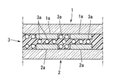
図6に、異方性導電材3を介して圧着された第1回路基板1と第2回路基板2の接続部分を模式的に拡大して示す。このように、第1回路基板1と第2回路基板2の対向電極1a,2aは、異方性導電材3に含まれている導電粒子3aによって電気的に接続される。
【0012】
対向電極1a,2a間に存在する導電粒子3aの個数が多いほど、確実な電気的接続状態が得られるが、第1回路基板1と第2回路基板2とがずれて、極端な場合、対向電極1a,2a間に存在する導電粒子3aが1個になったときでも、対向電極1a,2aは導通する。
【0013】
しかしながら、位置ずれにより対向電極1a,2a間に存在する導電粒子3aの数が少なくなると、長期間にわたっての接続の信頼性が低下してしまう。したがって、長期間にわたって接続の高い信頼性を得るには、対向電極1a,2a間に所定数の導電粒子3aが存在し得るような対向面積が必要とされる。
【0014】
すなわち、対向電極1a,2a間のずれ量が所定値以下であることが必要とされるが、上記先行技術では、対向電極1a,2a間の接続の有無は検査し得るものの、対向電極1a,2a間のずれ量までを正確に検査することは難しい。
【0015】
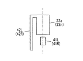
本発明は、上記した課題を解決するためになされたもので、その目的は、対向電極間のずれ量を電気的に容易に検査できるずれ量検出手段を備えた回路基板の接続構造を提供することにある。
【0016】
【課題を解決するための手段】
上記目的を達成するため、本発明は、短冊状の電極端子が所定のピッチで配列された第1電極端子群を有する第1回路基板と、上記第1電極端子群に対応する第2電極端子群を有する第2回路基板とを含み、上記第1電極端子群と上記第2電極端子群とを異方性導電材を介して電気的・機械的に接続する回路基板の接続構造において、いずれか一方の上記電極端子群に含まれる電極端子のうち、少なくとも両端に配置される端部電極端子の各々に、上記電極端子群の配列方向に沿う上記両回路基板間の相対的なずれ量を電気的に検出するずれ量検出手段が設けられており、上記ずれ量検出手段が、上記端部電極端子の電極端子群の中心側の内縁に沿う内縁延長線と上記端部電極端子の外縁に沿う外縁延長線とで挟まれる端部電極端子延長領域であって、かつ、いずれか他方の上記電極端子群に含まれる相手方端部電極端子が重ねられる領域内において、上記端部電極端子よりも狭い幅をもって上記端部電極端子とは電気的に絶縁して形成されたずれ量検出電極を備えていることを特徴としている。
【0017】
この構成によれば、上記相手方端部電極端子が上記ずれ量検出電極上に重ねられている場合には、上記端部電極端子と上記ずれ量検出電極とが上記相手方端部電極端子を介して導通状態となり、上記相手方端部電極端子が上記ずれ量検出電極から外れている場合には、上記端部電極端子と上記ずれ量検出電極は非導通となる。
【0018】
したがって、異方性導電材を介しての圧着後において、上記端部電極端子と上記ずれ量検出電極との間が、ショート(導通)であるかオープン(非導通)であるかを電気的に検査することにより、ずれ量の許容範囲内,許容範囲外を判定することができる。
【0019】
なお、上記ずれ量検出電極の幅は、上記第1電極端子群と上記第2電極端子群との間で許容されるずれ量に応じて、例えば端部電極端子の1/2幅,1/3幅などのように適宜決められる。
【0020】
上記端部電極端子と上記ずれ量検出電極との間のショート・オープン検査は、その双方にプローブを立てて行なわれるが、その作業を容易にするうえで、上記端部電極端子の一部分および上記ずれ量検出電極の一部分が、それぞれ上記相手方端部電極端子が重ねられる領域の外側に引き出されていることが好ましい。
【0021】
また、上記ずれ量検出電極が上記内縁延長線に接して配置されていることが好ましく、これによれば、上記端部電極端子の双方でショートであれば、ずれ量が許容範囲内と判定でき、いずれか一方の上記端部電極端子側でオープンであれば、ずれ量が許容範囲外と判定できる。
【0022】
上記端部電極端子を含めて電極端子が銅箔からなる場合、通常、その厚みは約35μmであり、これに対して、導電粒子の粒径は約10μm以下である。上記ずれ量検出電極は、上記端部電極端子よりも幅が狭く、しかも上記端部電極端子が上記のように上記内縁延長線に接して配置される場合には、その外縁側がブランク部分となり、異方性導電材による接着力が確保され難くなる。
【0023】
これを防止する意味で、上記ずれ量検出電極と、上記外縁延長線との間には、ずれ量の検出に関与しないダミー電極が上記ずれ量検出電極とは独立して形成されていることが好ましい。
【0024】
また、別の態様として、上記ずれ量検出電極は、その中心線が上記端部電極端子の中心線上に合致するように配置されていてもよく、これによっても、上記と同様な作用・効果が得られる。
【0025】
【発明の実施の形態】
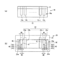
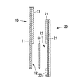
次に、図面を参照しながら、本発明の実施形態について説明する。図1(a)は第1回路基板10の電極接続部10aを示す平面図、図1(b)は第2回路基板20の電極接続部20aを示す平面図で、図2は第1回路基板10と第2回路基板20の各電極接続部10a,20aを異方性導電膜30を挟んで対向させた状態を示す断面図である。
【0026】
第1回路基板10と第2回路基板20は、ともにフレキシブル基板,ともに硬質基板もしくは一方がフレキシブル基板,他方が硬質基板のいずれの組み合わせであってもよい。なお、いずれか一方が例えば液晶パネルの端子部のようなITOからなる透明電極のリード端子を備えたガラス基板もしくはプラスチック基板であってもよい。また、異方性導電膜30に代えて、異方性導電樹脂が用いられてもよい。
【0027】
第1回路基板10と第2回路基板20とが、ともにフレキシブル基板であるとして、第1回路基板10の電極接続部10aには、ベースフィルム11上に形成された銅箔よりなる各リード配線から引き出された電極端子12a〜12n(nは特定の数を意味しない)を含む電極端子群12が露出されており、電極接続部10a以外の部分はレジスト膜13によって被覆されている。電極端子12a〜12nは短冊形状であって、所定のピッチで配列されている。なお、第1回路基板10の電極接続部10は、ベースフィルム11の端部に配置されている。
【0028】
第2回路基板20の電極接続部20aには、ベースフィルム21上に形成された銅箔よりなる各リード配線から引き出された電極端子22a〜22nを含む電極端子群22が露出されている。電極接続部20a以外の部分はレジスト膜23によって被覆されているが、この場合、電極接続部20aは窓枠状に開口されており、その周囲がレジスト膜23にて囲まれている。電極端子群22は電極端子群12と対応しており、電極端子22a〜22nの幅寸法および配列ピッチは、電極端子12a〜12nと同一である。
【0029】
なお、この例では、第2回路基板20の電極接続部20a上に異方性導電膜30を介して第1回路基板10の電極接続部10aを重ねるようにしており、したがって実際には、第1回路基板10の電極接続部10aは、図1(a)において紙面の裏側に位置している。
【0030】
また、この例において、第1回路基板10と第2回路基板20は、図2に示すように、電極接続部10aに対する電極端子群12の引き出し方向と、電極接続部20aに対する電極端子群22の引き出し方向とが同じ向きとなるようにして重ね合わされる。
【0031】
第1回路基板10側の電極端子群12に含まれる電極端子12a〜12nのうち、両端に位置する電極端子12a,12nを端部電極端子、同じく第2回路基板20側の電極端子群22に含まれる電極端子22a〜22nのうち、両端に位置する電極端子22a,22nを端部電極端子として、この例においては、第2回路基板20側の端部電極端子22a,22nの部分に、第1回路基板10と第2回路基板20との間のずれ量を検出するずれ量検出手段40がそれぞれ設けられている。
【0032】
このずれ量検出手段40は、端部電極端子22a側と端部電極端子22n側とで左右対称である点を除いて同一構成であるため、一方の端部電極端子22a側の構成要素には参照符号の末尾にLを付し、他方の端部電極端子22n側の構成要素には参照符号の末尾にRを付して、その構成を説明する。なお、他方の端部電極端子22n側の構成要素については、その参照符号を括弧内に記す。
【0033】
このずれ量検出手段40には、端部電極端子22a(22n)自体と、ずれ量検出電極41L(41R)とが含まれる。ずれ量検出電極41L(41R)は、端部電極端子22a(22n)の電極端子群の中心側の内縁IEに沿う内縁延長線と端部電極端子22a(22n)の外縁に沿う外縁延長線とで挟まれる端部電極端子延長領域であって、かつ、異方性導電膜30を介して相手方の端部電極端子12a(12n)が重ねられる領域(図4のハッチング部分)内に配置されている。
【0034】
ずれ量検出電極41L(41R)は、端部電極端子22a(22n)と同じく銅箔パターンよりなるが、端部電極端子22a(22n)とは電気的に絶縁するように形成されており、その幅W2は端部電極端子22a(22n)の幅W1よりも狭い。
【0035】
端部電極端子22a(22n)の電極端子群22の中心側寄りの縁を内縁IEとし、その反対側の縁を外縁OEとして、この例においては、ずれ量検出電極41L(41R)は、端部電極端子22a(22n)の内縁IEの延長線である内縁延長線に接するように配置されており、ずれの許容値に応じて、ずれ量検出電極41L(41R)の幅W2が選択される。
【0036】
例えば、第1回路基板10と第2回路基板20との間のずれの許容値を、端部電極端子22a(22n)の幅W1の1/2とするならばW2=W1/2に設定され、ずれの許容値を端部電極端子22a(22n)の幅W1の1/3とするならばW2=W1/3に設定される。なお、第1回路基板10側の電極端子を含めて他の電極端子の幅も、端部電極端子22a(22n)と同じくすべてW1である。
【0037】
本発明によると、第1回路基板10と第2回路基板20とを異方性導電膜30を介して圧着した後、端部電極端子22a(22n)とずれ量検出電極41L(41R)との間を対象として、導通チェッカーなどの検査器を用いて電気的なショート・オープン検査を実施することにより、回路基板10,20間のずれ量の良否判定を行うことができる。
【0038】
ショート・オープン検査には、図示しない2本のプローブが用いられる。すなわち、一方のプローブを端部電極端子22a(22n)側に接触させ、他方のプローブをずれ量検出電極41L(41R)側に接触させるのであるが、その作業を容易にするため、端部電極端子22a(22n)およびずれ量検出電極41L(41R)の各一部分を、相手方の端部電極端子12a(12n)が重ねられる領域の外側に引き出している。
【0039】
具体的に説明すると、この例においては、端部電極端子22a(22n)の外縁OE側からリード線42L(42R)を引き出して、このリード線42L(42R)の端部と、ずれ量検出電極41L(41R)の端部とを、電極接続部20aから反端部電極端子側に向けてレジスト膜23の下に潜り込ませるように延在させ、レジスト膜23の一部分にプローブ接触用として、それらの各端部を露出させるための開口部23aを形成している。
【0040】
ずれ量検出電極41L(41R)は、端部電極端子22a(22n)よりも幅が狭く、しかもずれ量検出電極41L(41R)が端部電極端子22a(22n)の内縁IE側寄りに配置されているため、ずれ量検出電極41L(41R)の脇(端部電極端子22a(22n)の外縁OE側)には、銅箔が存在しない比較的大きなブランク部分ができる。
【0041】
通常、パターンを形成する銅箔の厚みは約35μmであるため、銅箔が存在する部分と存在しないブランク部分とでは大きな高低差が生じ、ずれ量検出電極41L(41R)の接続安定性と、異方性導電膜30による接着力が確保され難くなる。
【0042】
これを防止する意味で、図1(b)に示すように、ずれ量検出電極41L(41R)の脇に、ずれ量の検出に関与しない銅箔よりなるダミー電極43L(43R)を、ずれ量検出電極41L(41R)と独立,離間して形成することが好ましい。
【0043】
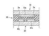
図3に、一方のずれ量検出電極41Lの脇にダミー電極43Lを形成した状態の断面図を示すが、これによれば、ずれ量検出電極41Lの近辺での高低差がなくなり、異方性導電膜30に含まれている粒子径が10μ以下の導電粒子3aによるずれ量検出電極41Lの接続安定性と、異方性導電膜30による接着力が確保されることになる。
【0044】
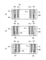
次に、図4(a)〜(c)を参照して、第1回路基板10と第2回路基板20とを異方性導電膜30を圧着した後において、上記したずれ量検出手段40を用いて、その相対的なずれ量の良否判定の仕方について説明する。なお、異方性導電膜30は、電極接続部10a,20aのほぼ全面にわたって配置される。また、ずれ量検出電極41L(41R)の幅W2は、W1/2幅であるとする。
【0045】
図4(a)は、第1回路基板10と第2回路基板20とが、それらの間にほとんどずれがない状態で接続された状態を示している。この場合、左側の端部電極端子22aとずれ量検出電極41Lとは、異方性導電膜30を介して相手方の端部電極端子12aにより導通され、また、右側の端部電極端子22nとずれ量検出電極41Rとは、異方性導電膜30を介して相手方の端部電極端子12nにより導通状態となる。したがって、ショート・オープン検査では、ずれ量検出電極41L−リード線42L間およびずれ量検出電極41R−リード線42R間は、ともにショートとなる。
【0046】
図4(b)は、第2回路基板20に対して第1回路基板10が左側にW1/2幅以上ずれた状態を示している。この場合、左側の端部電極端子22aにおいては、相手方の端部電極端子12aがずれ量検出電極41Lから外れる。これに対して、右側の端部電極端子22nでは、相手方の端部電極端子12nがずれ量検出電極41R上に存在している。したがって、ショート・オープン検査では、ずれ量検出電極41L−リード線42L間はオープンで、ずれ量検出電極41R−リード線42R間はショートとなる。
【0047】
図4(c)は図4(b)とは反対に、第2回路基板20に対して第1回路基板10が右側にW1/2幅以上ずれた状態を示している。この場合、左側の端部電極端子22aにおいては、相手方の端部電極端子12aがずれ量検出電極41L上に存在しており、これに対して、右側の端部電極端子22nでは、相手方の端部電極端子12nがずれ量検出電極41Rから外れる。したがって、ショート・オープン検査では、ずれ量検出電極41L−リード線42L間はショートで、ずれ量検出電極41R−リード線42R間はオープンとなる。
【0048】
このようにして、ずれ量検出電極41L−リード線42L間もしくはずれ量検出電極41R−リード線42R間のいずれか一方がオープンであれば、第1回路基板10と第2回路基板20とのずれ量が許容値(上記の例では、W1/2幅)を超えており、接続不良と判定することができる。
【0049】
変形例として、図5に示すように、ずれ量検出電極41L(41R)を端部電極端子22a(22n)に対して、例えばそれらの中心線を合わせて配置してもよい。この場合、第1回路基板10と第2回路基板20のずれが許容値を超えたときには、ずれ量検出電極41L−リード線42L間およびずれ量検出電極41R−リード線42R間はともにオープンとなる。
【0050】
なお、端部電極端子22a(22n)およびその相手方の端部電極端子12a(12n)は、ずれ量検出のためだけに設けられてもよいし、第1回路基板10と第2回路基板20との電気的な接続に関与する電極端子のいずれであってもよい。また、ずれ量検出手段40を第2回路基板20側ではなく、第1回路基板10側設けてもよい。
【0051】
【発明の効果】
以上説明したように、本発明によれば、第1回路基板側の電極端子群と第2回路基板側の電極端子群とを異方性導電材を介して電気的・機械的に接続する回路基板の接続構造において、いずれか一方の電極端子群に含まれる端部電極端子の各々に、その端部電極端子の電極端子群の中心側の内縁に沿う内縁延長線と端部電極端子の外縁に沿う外縁延長線とで挟まれる端部電極端子延長領域であって、かつ、いずれか他方の電極端子群に含まれる相手方端部電極端子が重ねられる領域内に、端部電極端子よりも狭いずれ許容幅を有するずれ量検出電極を形成したことにより、第1,第2回路基板の圧着後に、端部電極端子−ずれ量検出電極間を対象として電気的なショート・オープン検査を行うだけで、対向電極間のずれ量の良否判定を容易に行うことができる。
【図面の簡単な説明】
【図1】本発明の実施形態に係る第1回路基板および第2回路基板の各電極接続部を示す平面図。
【図2】上記第1回路基板および第2回路基板の対応関係を示す断面図。
【図3】本発明におけるずれ量検出電極部分を示す拡大断面図。
【図4】上記第1回路基板および第2回路基板のずれ量検出方法を説明するための模式図。
【図5】本発明におけるずれ量検出電極の変形例を示す平面図。
【図6】従来技術の説明において、異方性導電材による接続状態を示す拡大断面図。
【符号の説明】
10,20 回路基板
10a,20a 電極接続部
12,22 電極端子群
12a,12n,22a,22n 端部電極端子
30 異方性導電膜
40 ずれ量検出手段
41L,41R ずれ量検出電極
42L,42R リード線
43L,43R ダミー電極[0001]
TECHNICAL FIELD OF THE INVENTION
The present invention relates to a connection structure of a circuit board, and more specifically, a shift when electrically and mechanically connecting electrode terminal groups formed on two circuit boards via an anisotropic conductive material. It relates to an amount detecting means.
[0002]
[Prior art]
As a connection example of a circuit board, a field of a liquid crystal display element will be described. A control circuit board is connected to a terminal portion of a liquid crystal panel through a flexible board such as a TCP (tape carrier package) or a COF (chip on film). You.
[0003]
Anisotropic conductive materials that can electrically and mechanically connect a large number of electrode terminals collectively are often used for connecting the liquid crystal panel terminals to the flexible board and connecting the flexible board to the control circuit board. Have been.
[0004]
The anisotropic conductive material is, for example, a large number of conductive particles dispersed in a thermosetting resin, and is an electrical connection unit that exhibits conductivity in a single direction by thermocompression bonding. It is also a mechanical connection. The anisotropic conductive material includes a film-like anisotropic conductive film and a liquid anisotropic conductive resin.
[0005]
In the connection using an anisotropic conductive material, for example, an anisotropic conductive film is disposed between the electrode surface of one circuit board and the electrode surface of the other circuit board, and the respective electrode surfaces are overlapped and connected. Therefore, the connection state cannot be visually inspected unless one side is a transparent substrate like a terminal part of a liquid crystal panel.
[0006]
As this inspection method, methods of inspecting the state of pressure bonding by the strength of a peeling force (peeling force of a connection portion) or a method of protruding a resin have been known for a long time. Since it is difficult to check whether the inspection is performed, it is probably not reliable and a reliable inspection method.
[0007]
There is also a method of actually applying a test signal to each electrode after crimping to check whether there is continuity between the counter electrodes, but this requires a dedicated jig such as a connector for each circuit board, for example. In addition, when the number of electrodes is large, the inspection time becomes long, and thus it cannot be said that the inspection method is preferable.
[0008]
In view of this, the present applicant has previously proposed, for example, in Japanese Patent Application Laid-Open No. H11-15064, a technique capable of easily and reliably electrically inspecting a connection state between opposed electrodes regardless of the number of electrodes or the like.
[0009]
In this prior art, a pair of detection electrodes separated from each other are formed on both sides of an electrode terminal group of one circuit board, and the pair of detection electrodes are formed on both sides of an electrode terminal group of the other circuit board during regular alignment. A conduction electrode disposed between the detection electrodes is formed so that a shift between the electrode terminal groups is reflected on the pair of detection electrodes and the conduction electrode. By applying a probe to the detection electrode and measuring the conduction state between the detection electrodes, the presence or absence of connection between the counter electrodes can be inspected.
[0010]
[Patent Document 1]
JP-A-10-301137
[Problems to be solved by the invention]
FIG. 6 schematically shows a connection portion between the first circuit board 1 and the second circuit board 2 crimped via the anisotropic conductive material 3 in an enlarged scale. As described above, the opposing electrodes 1 a and 2 a of the first circuit board 1 and the second circuit board 2 are electrically connected by the conductive particles 3 a included in the anisotropic conductive material 3.
[0012]
As the number of the conductive particles 3a existing between the counter electrodes 1a and 2a increases, a more reliable electrical connection state can be obtained. However, when the first circuit board 1 and the second circuit board 2 are displaced from each other, in an extreme case, Even when the number of the conductive particles 3a existing between the electrodes 1a and 2a becomes one, the opposing electrodes 1a and 2a conduct.
[0013]
However, if the number of the conductive particles 3a existing between the opposing electrodes 1a and 2a is reduced due to the displacement, the reliability of the connection for a long time is reduced. Therefore, in order to obtain high connection reliability over a long period of time, a facing area where a predetermined number of conductive particles 3a can exist between the facing electrodes 1a and 2a is required.
[0014]
That is, it is necessary that the amount of displacement between the opposing electrodes 1a and 2a is equal to or less than a predetermined value. In the above-described prior art, the presence or absence of connection between the opposing electrodes 1a and 2a can be inspected. It is difficult to accurately inspect up to the displacement between 2a.
[0015]
SUMMARY OF THE INVENTION The present invention has been made to solve the above-described problem, and an object of the present invention is to provide a connection structure of a circuit board provided with a shift amount detection unit capable of easily electrically checking the shift amount between opposed electrodes. It is in.
[0016]
[Means for Solving the Problems]
To achieve the above object, the present invention provides a first circuit board having a first electrode terminal group in which strip-shaped electrode terminals are arranged at a predetermined pitch, and a second electrode terminal corresponding to the first electrode terminal group. A second circuit board having a group, wherein the first electrode terminal group and the second electrode terminal group are electrically and mechanically connected via an anisotropic conductive material via a circuit board connection structure. Of the electrode terminals included in one of the electrode terminal groups, at least each of the end electrode terminals disposed at both ends is provided with a relative shift amount between the two circuit boards along the arrangement direction of the electrode terminal group. Displacement amount detecting means for electrically detecting is provided, and the displacement amount detecting means is provided on an inner edge extension line along an inner edge on the center side of the electrode terminal group of the end electrode terminal and an outer edge of the end electrode terminal. End electrode terminal extension area sandwiched between outer edge extension lines along And, in a region where the other end electrode terminal included in one of the other electrode terminal groups overlaps, electrically insulates the end electrode terminal with a smaller width than the end electrode terminal. It is characterized by having a shift amount detection electrode formed in this way.
[0017]
According to this configuration, when the counterpart end electrode terminal is overlaid on the shift amount detection electrode, the end electrode terminal and the shift amount detection electrode are connected via the counterpart end electrode terminal. When the opposing end electrode terminal is deviated from the deviation amount detection electrode, the end electrode terminal and the deviation amount detection electrode become non-conductive.
[0018]
Therefore, after crimping via the anisotropic conductive material, it is electrically determined whether the end electrode terminal and the shift amount detection electrode are short (conductive) or open (non-conductive). By performing the inspection, it is possible to determine whether the deviation amount is within the allowable range or outside the allowable range.
[0019]
The width of the deviation amount detection electrode may be, for example, 幅 width of the end electrode terminal, 1/2 according to the deviation amount allowed between the first electrode terminal group and the second electrode terminal group. It is appropriately determined such as three widths.
[0020]
The short / open inspection between the end electrode terminal and the shift amount detection electrode is performed by setting up a probe on both of them, but in order to facilitate the work, a part of the end electrode terminal and the It is preferable that a part of the shift amount detection electrode is drawn out of the region where the counterpart end electrode terminal overlaps.
[0021]
Further, it is preferable that the shift amount detection electrode is disposed in contact with the inner edge extension line. According to this, if both of the end electrode terminals are short-circuited, the shift amount can be determined to be within an allowable range. If any one of the end electrode terminals is open, it can be determined that the shift amount is outside the allowable range.
[0022]
When the electrode terminals including the end electrode terminals are made of copper foil, the thickness is usually about 35 μm, whereas the particle size of the conductive particles is about 10 μm or less. The offset amount detection electrode is narrower than the end electrode terminal, and when the end electrode terminal is arranged in contact with the inner edge extension line as described above, the outer edge side becomes a blank portion. In addition, it is difficult to secure the adhesive force by the anisotropic conductive material.
[0023]
In order to prevent this, a dummy electrode that is not involved in the detection of the shift amount is formed between the shift amount detection electrode and the outer edge extension line independently of the shift amount detection electrode. preferable.
[0024]
Further, as another aspect, the displacement amount detection electrode may be arranged so that the center line thereof coincides with the center line of the end electrode terminal, and thereby, the same operation and effect as described above can be obtained. can get.
[0025]
BEST MODE FOR CARRYING OUT THE INVENTION
Next, an embodiment of the present invention will be described with reference to the drawings. FIG. 1A is a plan view showing an electrode connecting portion 10a of the first circuit board 10, FIG. 1B is a plan view showing an electrode connecting portion 20a of the second circuit board 20, and FIG. 2 is a first circuit board. FIG. 4 is a cross-sectional view showing a state in which the electrode connection portions 10 a and 20 a of the second circuit board 20 face each other with an anisotropic conductive film 30 interposed therebetween.
[0026]
The first circuit board 10 and the second circuit board 20 may be any combination of a flexible board, both a hard board or one of a flexible board and the other of a hard board. Note that one of them may be a glass substrate or a plastic substrate provided with a lead terminal of a transparent electrode made of ITO, such as a terminal portion of a liquid crystal panel. Further, instead of the anisotropic conductive film 30, an anisotropic conductive resin may be used.
[0027]
Assuming that the first circuit board 10 and the second circuit board 20 are both flexible boards, the electrode connection portions 10a of the first circuit board 10 are provided with respective lead wires made of copper foil formed on the base film 11. The electrode terminal group 12 including the extracted electrode terminals 12a to 12n (n does not mean a specific number) is exposed, and portions other than the electrode connection portions 10a are covered with a resist film 13. The electrode terminals 12a to 12n have a strip shape and are arranged at a predetermined pitch. In addition, the electrode connection part 10 of the first circuit board 10 is disposed at an end of the base film 11.
[0028]
An electrode terminal group 22 including electrode terminals 22a to 22n drawn from each lead wiring made of copper foil formed on the base film 21 is exposed at the electrode connection portion 20a of the second circuit board 20. The portion other than the electrode connection portion 20a is covered with the resist film 23. In this case, the electrode connection portion 20a is opened in a window frame shape, and the periphery thereof is surrounded by the resist film 23. The electrode terminal group 22 corresponds to the electrode terminal group 12, and the width dimension and arrangement pitch of the electrode terminals 22a to 22n are the same as those of the electrode terminals 12a to 12n.
[0029]
In this example, the electrode connection portion 10a of the first circuit board 10 is overlapped on the electrode connection portion 20a of the second circuit board 20 with the anisotropic conductive film 30 interposed therebetween. The electrode connection portion 10a of the one circuit board 10 is located on the back side of the drawing in FIG.
[0030]
Further, in this example, as shown in FIG. 2, the first circuit board 10 and the second circuit board 20 are connected to the electrode terminal group 12 with respect to the electrode connection part 10a and the electrode terminal group 22 with respect to the electrode connection part 20a. The sheets are superimposed so that the drawing direction is the same.
[0031]
Of the electrode terminals 12a to 12n included in the electrode terminal group 12 on the first circuit board 10, the electrode terminals 12a and 12n located at both ends are used as end electrode terminals, and the electrode terminals 22 on the second circuit board 20 are also used as electrode terminals. Of the included electrode terminals 22a to 22n, the electrode terminals 22a and 22n located at both ends are defined as end electrode terminals. In this example, the second electrode terminal 22a and 22n on the second circuit board 20 side are connected to the second electrode terminals 22a and 22n. A shift amount detecting means 40 for detecting a shift amount between the first circuit board 10 and the second circuit board 20 is provided.
[0032]
Since the displacement amount detecting means 40 has the same configuration except that the end electrode terminal 22a and the end electrode terminal 22n are symmetrical left and right, the components on one end electrode terminal 22a side include The configuration will be described by suffixing L to the end of the reference numerals and suffixing R to the components on the other end electrode terminal 22n side. In addition, about the component on the other end electrode terminal 22n side, the reference number is described in parentheses.
[0033]
The displacement amount detection means 40 includes the end electrode terminal 22a (22n) itself and a displacement amount detection electrode 41L (41R). The shift amount detection electrode 41L (41R) has an inner edge extension line along the center inner edge IE of the electrode terminal group of the end electrode terminals 22a (22n) and an outer edge extension line along the outer edge of the end electrode terminals 22a (22n). Are arranged in a region (hatched portion in FIG. 4) which is an end electrode terminal extension region sandwiched between the two and overlaps with the other end electrode terminal 12a (12n) via the anisotropic conductive film 30. I have.
[0034]
The displacement detection electrode 41L (41R) is made of a copper foil pattern like the end electrode terminal 22a (22n), but is formed so as to be electrically insulated from the end electrode terminal 22a (22n). The width W2 is smaller than the width W1 of the end electrode terminal 22a (22n).
[0035]
In this example, the edge near the center of the electrode terminal group 22 of the end electrode terminals 22a (22n) is defined as an inner edge IE, and the opposite edge is defined as an outer edge OE. It is arranged so as to be in contact with an inner edge extension line which is an extension of the inner edge IE of the internal electrode terminal 22a (22n), and the width W2 of the shift amount detection electrode 41L (41R) is selected according to the allowable shift value. .
[0036]
For example, if the allowable value of the displacement between the first circuit board 10 and the second circuit board 20 is の of the width W1 of the end electrode terminal 22a (22n), W2 = W1 / 2 is set. If the allowable value of the deviation is 1/3 of the width W1 of the end electrode terminal 22a (22n), W2 = W1 / 3. The widths of the other electrode terminals including the electrode terminals on the first circuit board 10 side are all W1 like the end electrode terminals 22a (22n).
[0037]
According to the present invention, after the first circuit board 10 and the second circuit board 20 are pressure-bonded via the anisotropic conductive film 30, the end electrode terminals 22a (22n) and the shift amount detection electrodes 41L (41R) are connected. By performing an electrical short / open test using a tester such as a continuity checker for the gap between the circuit boards, it is possible to determine whether or not the amount of deviation between the circuit boards 10 and 20 is good.
[0038]
Two probes (not shown) are used for the short / open inspection. That is, one probe is brought into contact with the end electrode terminals 22a (22n) and the other probe is brought into contact with the displacement detection electrodes 41L (41R). Each part of the terminal 22a (22n) and the shift amount detection electrode 41L (41R) is drawn out of the region where the other end electrode terminal 12a (12n) overlaps.
[0039]
More specifically, in this example, the lead wire 42L (42R) is pulled out from the outer edge OE side of the end electrode terminal 22a (22n), and the end of the lead wire 42L (42R) and the displacement detection electrode The end of 41L (41R) is extended from the electrode connecting portion 20a toward the opposite end electrode terminal side so as to be sunk under the resist film 23, and a part of the resist film 23 is used for probe contact. An opening 23a for exposing each of the ends is formed.
[0040]
The shift amount detection electrode 41L (41R) is narrower in width than the end electrode terminal 22a (22n), and the shift amount detection electrode 41L (41R) is arranged closer to the inner edge IE side of the end electrode terminal 22a (22n). Therefore, a relatively large blank portion free of copper foil is formed on the side of the shift amount detection electrode 41L (41R) (on the outer edge OE of the end electrode terminal 22a (22n)).
[0041]
Usually, since the thickness of the copper foil forming the pattern is about 35 μm, a large difference in height occurs between the portion where the copper foil is present and the blank portion where the copper foil is not present, and the connection stability of the displacement detection electrode 41L (41R) is improved. It becomes difficult to secure the adhesive force by the anisotropic conductive film 30.
[0042]
In order to prevent this, as shown in FIG. 1B, a dummy electrode 43L (43R) made of a copper foil which is not involved in the detection of the shift amount is provided beside the shift amount detection electrode 41L (41R). It is preferable to form the detection electrode 41L (41R) independently and apart from it.
[0043]
FIG. 3 is a cross-sectional view showing a state in which a dummy electrode 43L is formed beside one of the displacement amount detection electrodes 41L. According to this, a height difference near the displacement amount detection electrode 41L is eliminated, and The connection stability of the displacement detection electrode 41L by the conductive particles 3a having a particle diameter of 10 μm or less contained in the conductive film 30 and the adhesive force by the anisotropic conductive film 30 are secured.
[0044]
Next, referring to FIGS. 4A to 4C, after the first circuit board 10 and the second circuit board 20 are pressure-bonded with the anisotropic conductive film 30, the above-described displacement amount detecting means 40 is used. The method of determining the quality of the relative deviation will be described with reference to FIGS. In addition, the anisotropic conductive film 30 is disposed over substantially the entire surface of the electrode connecting portions 10a and 20a. Further, the width W2 of the displacement amount detection electrode 41L (41R) is assumed to be W1 / 2 width.
[0045]
FIG. 4A shows a state in which the first circuit board 10 and the second circuit board 20 are connected in a state where there is almost no displacement between them. In this case, the left end electrode terminal 22a and the shift amount detection electrode 41L are electrically connected to each other by the other end electrode terminal 12a via the anisotropic conductive film 30, and are shifted from the right end electrode terminal 22n. With the amount detection electrode 41R, the other end electrode terminal 12n becomes conductive through the anisotropic conductive film 30. Therefore, in the short / open inspection, both the gap between the displacement detection electrode 41L and the lead 42L and the gap between the displacement detection electrode 41R and the lead 42R are short-circuited.
[0046]
FIG. 4B shows a state in which the first circuit board 10 is shifted to the left side by more than W1 / 2 width with respect to the second circuit board 20. In this case, in the left end electrode terminal 22a, the other end electrode terminal 12a is displaced from the displacement detection electrode 41L. On the other hand, in the right end electrode terminal 22n, the counterpart end electrode terminal 12n exists on the shift amount detection electrode 41R. Therefore, in the short / open inspection, the gap between the displacement detection electrode 41L and the lead wire 42L is open, and the gap between the displacement detection electrode 41R and the lead wire 42R is short.
[0047]
FIG. 4C shows a state in which the first circuit board 10 is shifted to the right with respect to the second circuit board 20 by the width of W1 / 2 or more, contrary to FIG. 4B. In this case, in the left end electrode terminal 22a, the other end electrode terminal 12a is present on the shift amount detection electrode 41L, whereas in the right end electrode terminal 22n, the other end electrode terminal 22n is located at the other end electrode terminal 22a. The partial electrode terminal 12n comes off the displacement detection electrode 41R. Therefore, in the short / open inspection, the gap between the displacement detection electrode 41L and the lead wire 42L is short, and the gap between the displacement detection electrode 41R and the lead wire 42R is open.
[0048]
In this way, if any one of the gap between the shift amount detection electrode 41L and the lead wire 42L or the gap between the shift amount detection electrode 41R and the lead wire 42R is open, the shift between the first circuit board 10 and the second circuit board 20 is performed. The amount exceeds the allowable value (W1 / 2 width in the above example), and it can be determined that the connection is poor.
[0049]
As a modified example, as shown in FIG. 5, the displacement detection electrodes 41L (41R) may be arranged with respect to the end electrode terminals 22a (22n), for example, with their center lines aligned. In this case, when the displacement between the first circuit board 10 and the second circuit board 20 exceeds an allowable value, both the gap between the displacement detection electrode 41L and the lead 42L and the gap between the displacement detection electrode 41R and the lead 42R are open. .
[0050]
Note that the end electrode terminals 22a (22n) and the end electrode terminals 12a (12n) of the other end may be provided only for detecting the amount of displacement, or the first circuit board 10 and the second circuit board 20 may be provided separately. May be any of the electrode terminals involved in the electrical connection. Further, the shift amount detecting means 40 may be provided on the first circuit board 10 side instead of the second circuit board 20 side.
[0051]
【The invention's effect】
As described above, according to the present invention, a circuit for electrically and mechanically connecting an electrode terminal group on a first circuit board side and an electrode terminal group on a second circuit board side via an anisotropic conductive material. In the connection structure of the substrate, each of the end electrode terminals included in any one of the electrode terminal groups is provided with an inner edge extension line along an inner edge on the center side of the electrode terminal group of the end electrode terminal and an outer edge of the end electrode terminal. In the end electrode terminal extension region sandwiched between the outer electrode extension line along with, and in a region where the other end electrode terminal included in either of the other electrode terminal group is overlapped, it is narrower than the end electrode terminal. The formation of the displacement detection electrode having an allowable width in the end, after the crimping of the first and second circuit boards, requires only an electrical short / open inspection for the portion between the end electrode terminal and the displacement detection electrode. , Easy to determine the quality of the deviation between the opposing electrodes Ukoto can.
[Brief description of the drawings]
FIG. 1 is a plan view showing electrode connection portions of a first circuit board and a second circuit board according to an embodiment of the present invention.
FIG. 2 is a sectional view showing the correspondence between the first circuit board and the second circuit board.
FIG. 3 is an enlarged cross-sectional view showing a displacement amount detection electrode part according to the present invention.
FIG. 4 is a schematic diagram for explaining a method for detecting a shift amount between the first circuit board and the second circuit board.
FIG. 5 is a plan view showing a modification of the displacement detection electrode according to the present invention.
FIG. 6 is an enlarged cross-sectional view showing a connection state using an anisotropic conductive material in the description of the related art.
[Explanation of symbols]
10, 20 Circuit board 10a, 20a Electrode connection part 12, 22 Electrode terminal group 12a, 12n, 22a, 22n End electrode terminal 30 Anisotropic conductive film 40 Shift amount detecting means 41L, 41R Shift amount detecting electrodes 42L, 42R Lead Line 43L, 43R Dummy electrode