JP2004159372A - Antenna - Google Patents
Antenna Download PDFInfo
- Publication number
- JP2004159372A JP2004159372A JP2004051839A JP2004051839A JP2004159372A JP 2004159372 A JP2004159372 A JP 2004159372A JP 2004051839 A JP2004051839 A JP 2004051839A JP 2004051839 A JP2004051839 A JP 2004051839A JP 2004159372 A JP2004159372 A JP 2004159372A
- Authority
- JP
- Japan
- Prior art keywords
- antenna
- assembly
- probe
- layer
- antenna according
- Prior art date
- Legal status (The legal status is an assumption and is not a legal conclusion. Google has not performed a legal analysis and makes no representation as to the accuracy of the status listed.)
- Granted
Links
- 239000000463 material Substances 0.000 claims abstract description 63
- 239000000523 sample Substances 0.000 claims abstract description 38
- 230000035699 permeability Effects 0.000 claims abstract description 29
- 238000001914 filtration Methods 0.000 claims abstract description 10
- 230000005855 radiation Effects 0.000 claims abstract description 10
- 229910052751 metal Inorganic materials 0.000 claims description 11
- 239000002184 metal Substances 0.000 claims description 11
- 238000010586 diagram Methods 0.000 claims description 7
- 230000000737 periodic effect Effects 0.000 claims description 7
- 230000010287 polarization Effects 0.000 claims description 5
- 238000000034 method Methods 0.000 claims description 3
- 230000005540 biological transmission Effects 0.000 abstract description 4
- TWNQGVIAIRXVLR-UHFFFAOYSA-N oxo(oxoalumanyloxy)alumane Chemical compound O=[Al]O[Al]=O TWNQGVIAIRXVLR-UHFFFAOYSA-N 0.000 description 9
- 239000003989 dielectric material Substances 0.000 description 3
- 239000000696 magnetic material Substances 0.000 description 3
- 230000009977 dual effect Effects 0.000 description 2
- 230000009286 beneficial effect Effects 0.000 description 1
- 239000000919 ceramic Substances 0.000 description 1
- 238000010276 construction Methods 0.000 description 1
- 238000005516 engineering process Methods 0.000 description 1
- 230000006698 induction Effects 0.000 description 1
- 239000007769 metal material Substances 0.000 description 1
- 150000002739 metals Chemical class 0.000 description 1
- 229920003023 plastic Polymers 0.000 description 1
- 239000004033 plastic Substances 0.000 description 1
- 238000007747 plating Methods 0.000 description 1
- 229910000859 α-Fe Inorganic materials 0.000 description 1
Images


Classifications
-
- H—ELECTRICITY
- H01—ELECTRIC ELEMENTS
- H01Q—ANTENNAS, i.e. RADIO AERIALS
- H01Q19/00—Combinations of primary active antenna elements and units with secondary devices, e.g. with quasi-optical devices, for giving the antenna a desired directional characteristic
- H01Q19/06—Combinations of primary active antenna elements and units with secondary devices, e.g. with quasi-optical devices, for giving the antenna a desired directional characteristic using refracting or diffracting devices, e.g. lens
- H01Q19/062—Combinations of primary active antenna elements and units with secondary devices, e.g. with quasi-optical devices, for giving the antenna a desired directional characteristic using refracting or diffracting devices, e.g. lens for focusing
-
- H—ELECTRICITY
- H01—ELECTRIC ELEMENTS
- H01Q—ANTENNAS, i.e. RADIO AERIALS
- H01Q1/00—Details of, or arrangements associated with, antennas
- H01Q1/40—Radiating elements coated with or embedded in protective material
-
- H—ELECTRICITY
- H01—ELECTRIC ELEMENTS
- H01Q—ANTENNAS, i.e. RADIO AERIALS
- H01Q15/00—Devices for reflection, refraction, diffraction or polarisation of waves radiated from an antenna, e.g. quasi-optical devices
- H01Q15/0006—Devices acting selectively as reflecting surface, as diffracting or as refracting device, e.g. frequency filtering or angular spatial filtering devices
- H01Q15/006—Selective devices having photonic band gap materials or materials of which the material properties are frequency dependent, e.g. perforated substrates, high-impedance surfaces
-
- H—ELECTRICITY
- H01—ELECTRIC ELEMENTS
- H01Q—ANTENNAS, i.e. RADIO AERIALS
- H01Q19/00—Combinations of primary active antenna elements and units with secondary devices, e.g. with quasi-optical devices, for giving the antenna a desired directional characteristic
- H01Q19/005—Patch antenna using one or more coplanar parasitic elements
-
- H—ELECTRICITY
- H01—ELECTRIC ELEMENTS
- H01Q—ANTENNAS, i.e. RADIO AERIALS
- H01Q19/00—Combinations of primary active antenna elements and units with secondary devices, e.g. with quasi-optical devices, for giving the antenna a desired directional characteristic
- H01Q19/06—Combinations of primary active antenna elements and units with secondary devices, e.g. with quasi-optical devices, for giving the antenna a desired directional characteristic using refracting or diffracting devices, e.g. lens
-
- H—ELECTRICITY
- H01—ELECTRIC ELEMENTS
- H01Q—ANTENNAS, i.e. RADIO AERIALS
- H01Q19/00—Combinations of primary active antenna elements and units with secondary devices, e.g. with quasi-optical devices, for giving the antenna a desired directional characteristic
- H01Q19/10—Combinations of primary active antenna elements and units with secondary devices, e.g. with quasi-optical devices, for giving the antenna a desired directional characteristic using reflecting surfaces
Abstract
Description
本発明は、マイクロ波範囲において高度な周波数指向性を達成する送信または受信アンテナに関する。 The present invention relates to a transmitting or receiving antenna that achieves high frequency directivity in the microwave range.
電気エネルギーを電磁エネルギーにおよびその逆に変換することができる少なくとも1つのプローブを備えるアンテナが知られている。
現在、通常使用されているアンテナは、特に、パラボラ反射器アンテナ、レンズ・アンテナおよびホーン・アンテナである。
Antennas with at least one probe capable of converting electrical energy to electromagnetic energy and vice versa are known.
Currently used antennas are, in particular, parabolic reflector antennas, lens antennas and horn antennas.
パラボラ反射器アンテナは放物線形の反射面を備え、反射面の焦点にプローブが配置される。このため、アンテナはパラボラ反射器の焦点長さに対して一定のサイズでなければならない。 The parabolic reflector antenna has a parabolic reflecting surface, and the probe is located at the focal point of the reflecting surface. For this reason, the antenna must be of a fixed size for the focal length of the parabolic reflector.
レンズ・アンテナはレンズを備え、レンズの焦点にプローブが配置される。焦点長さのためにサイズが大きくなる他に、この種のアンテナはレンズの重量のせいで重く、この重量のためある種の用途には使用できない場合がある。 The lens antenna comprises a lens, and a probe is located at the focal point of the lens. In addition to being large in size due to focal length, such antennas are heavy due to the weight of the lens and may not be usable for certain applications due to this weight.
ホーン・アンテナは、高い指向性を得るためには体積および重量が大きくなければならない。 Horn antennas must be large in volume and weight to achieve high directivity.
本発明は、高い指向性で電磁波を送信または受信できながら体積および重量がより小さいアンテナを作ることによって、従来のアンテナの短所を克服する。 The present invention overcomes the shortcomings of conventional antennas by creating an antenna that is small in volume and weight while transmitting or receiving electromagnetic waves with high directivity.
本発明は、従って、電気エネルギーを電磁エネルギーにおよびその逆に変換することができる少なくとも1つのプローブを備えるアンテナに関するものであり、このアンテナが、さらに、その誘電率および/または透磁率および/または導電率の異なる少なくとも2つの材料で作られるエレメントのアセンブリを備え、その内部にプローブが配置され、アセンブリ内でのエレメントの配列が、プローブによって生成または受信される電磁波の放射および空間周波数フィルタリングを保証し、このフィルタリングにより、特に周波数バンド・ギャップ内においてアンテナの1つまたはそれ以上の動作周波数が許容されることを特徴とする。 The present invention therefore relates to an antenna comprising at least one probe capable of converting electrical energy to electromagnetic energy and vice versa, the antenna further comprising its dielectric constant and / or permeability and / or Includes an assembly of elements made of at least two materials of differing electrical conductivity, with a probe placed inside, the arrangement of elements in the assembly ensures radiation and spatial frequency filtering of electromagnetic waves generated or received by the probe However, this filtering is characterized in that one or more operating frequencies of the antenna are allowed, especially in the frequency band gap.
従って、このアンテナは、単純化された給電システムおよびその誘電率および/または透磁率および/または導電率の異なる材料で作られるエレメントの薄いアセンブリを使用することによって、サイズおよび重量を減少することができる。 Thus, this antenna can be reduced in size and weight by using a simplified feeding system and a thin assembly of elements made of materials with different dielectric and / or magnetic and / or electrical conductivity. it can.
本発明によるアンテナは、また、以下の特徴のうち1つまたはそれ以上を持つことができる。
−エレメントのアセンブリが、その構造において少なくとも一次元の周期性、および少なくとも内部に1つのキャビティを生成する1つの欠落部を有する。
−エレメントのアセンブリが、所与の誘電率、透磁率および導電率を有する第1の材料を備え、これが、その誘電率および/または透磁率および/または導電率が異なる他の2つの材料の構造の内部にキャビティを形成し、この構造が他の2つの材料の3つの別個の空間的方向に三重の周期性を有する。
−エレメントのアセンブリが、所与の誘電率、透磁率および導電率を有する第1の材料を備え、これが、その誘電率および/または透磁率および/または導電率が異なる他の2つの材料の構造内にキャビティを形成し、この構造が他の2つの材料の2つの別個の空間的方向に二重の周期性を有する。
−エレメント・アセンブリが、その誘電率および/または透磁率および/または導電率の異なる材料の平らな層によって構成される。
−エレメント・アセンブリが、所与の誘電率、透磁率および導電率を有する材料の第1の平らな層を備え、その内部にプローブが配置され、第1の層が、一次元の周期パターンに配列される誘電率および/または透磁率および/または導電率の異なる材料の少なくとも1連続の平らな層と接触する。
−さらに、プローブを支え、エレメントのアセンブリと接して配置される平面電磁波反射器を備える。
An antenna according to the invention may also have one or more of the following features.
The assembly of the elements has at least a one-dimensional periodicity in its structure and at least one missing part creating at least one cavity therein;
The assembly of the elements comprises a first material having a given dielectric constant, magnetic permeability and electrical conductivity, which is the structure of the other two materials whose dielectric constant and / or magnetic permeability and / or electrical conductivity are different Form a cavity inside, the structure having a triple periodicity in three distinct spatial directions of the other two materials.
The assembly of the elements comprises a first material having a given permittivity, magnetic permeability and electrical conductivity, which is the structure of the other two materials whose dielectric constant and / or magnetic permeability and / or electrical conductivity are different A cavity is formed in this structure having a dual periodicity in two distinct spatial directions of the other two materials.
The element assembly is constituted by flat layers of materials having different dielectric constants and / or permeability and / or conductivity;
The element assembly comprises a first flat layer of a material having a given permittivity, magnetic permeability and conductivity, in which the probe is arranged, the first layer being arranged in a one-dimensional periodic pattern; Contacting at least one continuous flat layer of materials of different dielectric and / or magnetic permeability and / or conductivity arranged.
It further comprises a planar electromagnetic wave reflector supporting the probe and arranged in contact with the assembly of the elements;
アンテナは、プローブを配置するための金属プレートを備え、金属プレートは、所与の誘電率、透磁率および導電率を有する材料の第1の平らな層と接触する平面反射器を形成し、第1の平らな層の厚みe1は式e1=0.5(λ/√εrμr)によって与えられ、第1の層自体は、その誘電率および/または透磁率および/または導電率が異なる材料の1連続の平らな層と接触し、平らな層の各々の厚みeは式e1=0.25(λ/√εrμr)によって与えられる。ここでラムダ(λ)はユーザが望むアンテナの動作周波数に対応する波長であり、εrおよびμrは、それぞれ当該平らな層の材料の比誘電率および比透磁率である。 The antenna comprises a metal plate for placing a probe, the metal plate forming a planar reflector in contact with a first planar layer of a material having a given permittivity, magnetic permeability and conductivity, and The thickness e 1 of one flat layer is given by the equation e 1 = 0.5 (λ / √ε r μ r ), the first layer itself having different dielectric constant and / or permeability and / or conductivity In contact with a continuous flat layer of material, the thickness e of each of the flat layers is given by the equation e 1 = 0.25 (λ / √ε r μ r ). Here, lambda (λ) is the wavelength corresponding to the operating frequency of the antenna desired by the user, and ε r and μ r are the relative permittivity and relative permeability of the material of the flat layer, respectively.
単純化された給電システムおよびその誘電率および/または透磁率および/または導電率の異なる材料で作られるエレメントの薄いアセンブリを使用することによって、サイズおよび重量を減少することができる。 The size and weight can be reduced by using a simplified power supply system and a thin assembly of elements made of materials with different dielectric and / or magnetic and / or electrical conductivity.
本発明は、単に例として示され下記の添付図面を参照して、より容易に理解されるだろう。 The present invention will be more readily understood with reference to the accompanying drawings, given by way of example only, and in which:
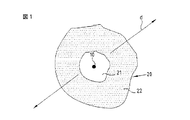
図1に示すように、本発明によるアンテナは、以下のものを備える。すなわち、電気波を電磁波にまたその逆に変換することができるプローブ10である。例えば、プレート・アンテナ、ダイポール・アンテナ、円偏極アンテナ、スロット・アンテナおよび共面プレート・ワイヤ・アンテナなどのアンテナは、本発明によるアンテナにおいてプローブ10として使用するのに適している。
As shown in FIG. 1, the antenna according to the present invention includes: That is, the
その誘電率および/または透磁率および/または導電率が異なる少なくとも2つの材料で作られるエレメントのアセンブリ20の内部にプローブ10が配置される。プラスティック、セラミック、フェライト、金属など、低損失の材料を使用することが望ましい。
The
本発明の1つの長所は、設計者が要求する分極のタイプ(線形または円形)、楕円率および電気特性を満たし、同時にこのプローブ10がアンテナの全体寸法に比べて小さくなければならないことを条件として、プローブ10の設計が非常に単純である点である。
One advantage of the present invention is that it meets the type of polarization (linear or circular), ellipticity, and electrical properties required by the designer, while at the same time providing that this
アセンブリ20の1つの利点は、これが、1つまたはそれ以上の認可空間方向dで1つのバンド・ギャップ内において1つまたはそれ以上の伝搬周波数モードを許容するアンテナの設計を可能にすることであり、空間フィルタリング自体は、周波数およびアセンブリ20が含む材料の性質に依存する。
One advantage of
内部に1つまたはそれ以上のキャビティ21が存在する光子禁止帯を持つ材料の原理に基づいて設計される構造22を備えるこのアセンブリ20の別の長所は、その最も隣接するものから非常によく絶縁された1つまたはそれ以上の伝搬周波数モードを持つことである。
Another advantage of this
光子禁止帯を持つ材料の原理に基づいて設計される構造は、その誘電率および/または透磁率および/または導電率の異なるエレメントの構造であり、この構造は少なくとも一次元の周期性を持つ。 A structure designed based on the principle of a material having a photon forbidden band is a structure of elements having different permittivity and / or magnetic permeability and / or conductivity, and this structure has at least one-dimensional periodicity.
アセンブリ20内部に配置されるキャビティ21は、光子禁止帯22を持つ材料と結合することによって、技術上、欠落部の光子禁止帯材料として知られる材料の性質をアセンブリに与える。
The
これは、
−使用される材料の誘電特性および/または磁気特性および/または導電特性を局部的に修正し、
−1つまたはそれ以上の材料の寸法を局部的に修正することができる。
this is,
Locally modifying the dielectric and / or magnetic and / or conductive properties of the materials used;
One or more material dimensions can be locally modified.
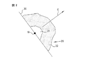
図2に示される本発明によるアンテナは、アセンブリ20の真中に配置されプローブ10を含む電磁反射面30を備えることもでき、特に放射が半空間においてのみ有益である場合にはアンテナの寸法を半分に縮小できるようにする。
The antenna according to the invention shown in FIG. 2 can also comprise an electromagnetic reflecting
電磁反射面30を備える本発明によるアンテナの1つの利点は、このアンテナの指向性を示す図における主たる突出部での利得を増大することである。
One advantage of the antenna according to the invention with the electromagnetic reflecting
図3に示される本発明によるアンテナは、一次元の周期性を有する光子禁止帯を持つ材料の原理に基づく構造22を備える。すなわち、この構造22は、それぞれ誘電率および/または透磁率および/または導電率の異なる2つの材料23および24、例えばアルミニウム酸化物と空気との交互の平らな層を備える。
The antenna according to the invention shown in FIG. 3 comprises a
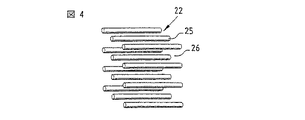
図4に示される本発明によるアンテナは、二次元の周期性を有する光子禁止帯の材料の原理に基づく構造22を備える。すなわち、この構造22は、第2の材料26例えば空気によって相互に分離される規則正しく配置される第1の材料例えばアルミニウム酸化物の円筒形のバー25を備え、第2の材料はその誘電率および/または透磁率および/または導電率が第1の材料と異なる。
The antenna according to the invention shown in FIG. 4 comprises a
例えば、この構造は重ねられた層の連続で配列される円筒形のバーで構成される。 For example, the structure consists of cylindrical bars arranged in a series of stacked layers.
各層において、バーは相互に平行に伸び、規則正しい間隔で配列される。 In each layer, the bars extend parallel to one another and are arranged at regular intervals.
さらに、連続層のバーは、規則正しい間隔で整合される。バーは金属で作られることが望ましい。 In addition, the bars of successive layers are aligned at regular intervals. The bar is preferably made of metal.
図5に示される本発明によるアンテナは、構造22が、第2の材料28例えば空気によって相互に分離された第1の材料例えばアルミニウム酸化物または金属の例えば直方体の均等に配列される交互のバー27を含むように、三次元の周期性を有する光子禁止帯を持つ材料の原理に基づく構造22を備え、第2の材料はその誘電率および/または透磁率および/または導電率が第1の材料と異なる。
The antenna according to the invention shown in FIG. 5 comprises an equally arranged alternating bar of
例えば、構造22は、層の積み重ね状に配列された本質的に直方体のバーで構成される。各層において、バーは相互に平行に伸び、規則正しい間隔で配置され、隣接する2つの層のバーは一定の角度例えば90°を形成する。
For example,
さらに、中間層によって分離される層のバーは相互に平行であり、規則正しい間隔で整合される。 Furthermore, the bars of the layers separated by the intermediate layer are parallel to one another and are aligned at regular intervals.
図6を参照すると、本発明によるアンテナの好適な実施態様は、次のものを備える。
−単一の給電線11を使用するプレート・プローブ10a。このプローブの長所は、その構造が非常に単純であり、アンテナの金属および誘電損失を制限することである。
−平面電磁反射器30aを形成する金属プレート。
−平面反射器30aと接触するキャビティ21aを形成する平らな層。このキャビティ21aは、表面波の誘導を制限するように、できれば低誘電率または低透磁率の材料によって構成されるが、図6に示されるようにこの材料を例えば空気とすることができる。
−構造22。誘電率および/または透磁率および/または導電率が異なるその材料23a、24a、23bは、一次元の周期パターンで連続的な平らな層に配列される。
Referring to FIG. 6, a preferred embodiment of the antenna according to the present invention comprises:
A
A metal plate forming the planar
A flat layer forming a
-
アンテナの平面に対して直角の方向に使用できる周期の数は、使用される材料の誘電率および/または透磁率および/または導電率の対比(コントラスト)に依存する。周期の数を少なくするためには、異なる材料間の指標の対比を増大しなければならない。 The number of periods that can be used in a direction perpendicular to the plane of the antenna depends on the relative permittivity and / or permeability and / or conductivity of the material used (contrast). To reduce the number of periods, the contrast of the index between different materials must be increased.
例えば、図6に示される実施態様において、使用される材料は、高誘電率のアルミニウム酸化物および低誘電率の空気であり、構造22は材料の層を3層持つだけでよい。
For example, in the embodiment shown in FIG. 6, the materials used are high-k aluminum oxide and low-k air, and the
従って、構造22は、第2の空気の平らな層24aと接触する第1のアルミニウム酸化物の層23aを含み、空気の層は第3のアルミニウム酸化物の層23bと接触する。
Thus,
誘電材料または磁気材料の連続的な平らな層のアセンブリ20の第1の層21aがキャビティを構成し、その後の層23a、24aおよび23bが構造22を構成する、図6に示される実施態様において、
a) 比誘電率εrおよび比透磁率μrである材料から成る平らな層21aの厚みe21aは、式e21a≒0.5 (λ/√εrμr)によって与えられる。ここで、λはアンテナの動作周波数に対応する波長であり、記号「≒」は「等しいかあるいはほぼ等しい」を意味する。
例えば、図6に示される空気の平らな層21aの厚みは、e21a=0.5λに等しい。
b) 構造22内の比誘電率εrおよび比透磁率μrである誘電材料または磁気材料から成る平らな層の厚みeは、式e≒0.25 (λ/√εrμr)によって与えられる。
例えば、図6に示されるアルミニウム酸化物23aの平らな層の厚みは、e23a=0.08λに等しく、図6に示される空気の平らな層24aの厚みはe24a=0.25λに等しく、図6に示されるアルミニウム酸化物の平らな層23bの厚みは、ほぼe23a=0.08λに等しい。
c) 構造22、プレート30aおよびキャビティ21aの横寸法は、アンテナに要求される利得の関数として選択される。アンテナの有益な形状は円形として表され、その直径Φは、以下の既知の経験式GdB≧20log(πΦ/λ)−2.5に従って、目標の利得に合わせられる。
例えば、図8に示されるように20dBの利得を得るためには、本発明によるアンテナ・システムの横寸法は、4.3λである。その後、既知のプロセスを使ってアンテナの一定形状の放射を得るようにアンテナの横形状が選択される。
d) 図6において説明されるアンテナの構成に使用される様々な材料の層の上記の横寸法および厚みを考慮すると、アンテナの全体寸法は次のとおりである:厚みHは約λ、および横寸法Lは約4.3λ。従って、波長3cmに対応する10GHz動作周波数の場合、図6に示される本発明によるアンテナの特定の実施態様において、体積は約3×13×13cm3であるのに対して、焦点長さが約70cmである同じ周波数10GHzで動作する従来の椀形アンテナはかなりこれより大きいスペースを必要とする。
In the embodiment shown in FIG. 6, the
a) The thickness e 21a of the
For example, the thickness of the flat layer of
b) The thickness e of the flat layer of dielectric or magnetic material with relative permittivity ε r and relative permeability μ r in the
For example, the thickness of the flat layer of
c) The lateral dimensions of
For example, to obtain a gain of 20 dB as shown in FIG. 8, the lateral dimension of the antenna system according to the invention is 4.3λ. The lateral shape of the antenna is then selected to obtain a constant shape radiation of the antenna using known processes.
d) Considering the above lateral dimensions and thicknesses of the layers of various materials used in the construction of the antenna described in FIG. 6, the overall dimensions of the antenna are: thickness H is about λ, and lateral Dimension L is about 4.3λ. Therefore, if the 10GHz operating frequency corresponding to the wavelength 3 cm, in certain embodiments of the antenna according to the invention shown in FIG. 6, whereas the volume is about 3 × 13 × 13cm 3, the focal length of approximately A conventional bowl antenna operating at the same frequency of 10 GHz, which is 70 cm, requires considerably more space.
従って、本発明は、主に本発明によるアンテナの薄さによって、アンテナに関連するサイズの問題を解決するのに確実に役立つことは明らかである。 Thus, it is clear that the invention certainly helps to solve the size problem associated with the antenna, mainly due to the thinness of the antenna according to the invention.
さらに、図6に示される本発明によるアンテナの連続的な平らな層の厚みはλに比例し、従ってアンテナの動作周波数に反比例するので、本発明が実現されることにより、多層技術を使って非常に高い周波数で動作するアンテナを設計することが可能になる。 Further, since the thickness of the continuous flat layer of the antenna according to the invention as shown in FIG. 6 is proportional to λ and therefore inversely proportional to the operating frequency of the antenna, the invention is realized by using multilayer technology. It becomes possible to design antennas that operate at very high frequencies.
図6に示される本発明によるアンテナは、このアンテナによって生成または受信される電磁波が、放射され、図7に示される通り、空間周波数フィルタリングを受けるようにする。このフィルタリングにより、特に、周波数バンド・ギャップB内においてアンテナの1つまたはそれ以上の動作周波数fが許容される。 The antenna according to the invention shown in FIG. 6 allows the electromagnetic waves generated or received by this antenna to be radiated and subjected to spatial frequency filtering as shown in FIG. This filtering allows, among other things, one or more operating frequencies f of the antenna in the frequency band gap B.
図6に示される本発明によるアンテナは、20dBの利得を達成するように設計され、図8に示される通りの放射図を持つ。 The antenna according to the invention shown in FIG. 6 is designed to achieve a gain of 20 dB and has a radiation diagram as shown in FIG.
本発明によるアンテナは従来のアパーチャ・アンテナと同様、ある所定の方向において大きな利得を得ることにある。 The antenna according to the present invention, like a conventional aperture antenna, is to obtain a large gain in a predetermined direction.
また、この放射図において、2番目の大きさの突出部が小さいことも明らかである。 It is also evident in this emission diagram that the second largest protrusion is small.
図6に関連して説明されるアンテナの動作について、次に検証する。アンテナは2つの動作モード、すなわち送信モードおよび受信モードを有する。 The operation of the antenna described with reference to FIG. 6 will now be verified. The antenna has two modes of operation, a transmit mode and a receive mode.
送信モードにおいて、給電線11によって送られる電流はプローブ10aに達し、プローブは、電流を電磁波に変換する。この電磁波は、次にその誘電率および/または透磁率および/または導電率の異なる材料で作られるエレメントのアセンブリ20を通過する。このアセンブリの配列は、その構成により電磁波の空間周波数フィルタリングが可能であるので、ユーザが要求する特性に応じてアンテナ・システムの放射図を形成する。
In the transmission mode, the current sent by the
受信モードにおいては、アンテナに達した電磁波は、プローブ10aに達する前に、その誘電率および/または透磁率および/または導電率の異なる材料で作られるエレメントのアセンブリ20を通過するとき空間周波数フィルタリングされる。アンテナの構成によりユーザが要求する特性に応じてフィルタリングされる電磁波は、次にプローブ10aによって電流に変換されて、給電線11に送られる。
In the receiving mode, the electromagnetic waves reaching the antenna are spatially frequency filtered before reaching the
特定の実施態様によれば、アンテナのプローブは、性質上、アンテナにおいて線形もしくは円偏極を生成することができ、アンテナが線形偏極または円偏極によって動作するようにする。 According to a particular embodiment, the probe of the antenna can by nature produce a linear or circular polarization at the antenna, causing the antenna to operate with linear or circular polarization.
別の実施態様によれば、平らな層の形状は、放射源アパーチャ理論に従って目標の放射および利得図を得るように設計される。 According to another embodiment, the shape of the flat layer is designed to obtain a target radiation and gain diagram according to the source aperture theory.
さらに別の実施態様によれば、構造を構成するエレメントはプローブを取り囲む同軸円筒形であり、従って、この配列は放射状の周期性を有し、内側の円筒形エレメントはプローブを受けるキャビティを形成する。 According to yet another embodiment, the elements making up the structure are coaxial cylinders surrounding the probe, thus the arrangement has a radial periodicity, the inner cylindrical element forming a cavity for receiving the probe .
さらに別の実施態様によれば、構造22を構成するエレメントは、二次元または三次元の周期性を有する光子禁止帯を持つ材料から成る同軸円筒形である。
According to yet another embodiment, the elements making up
本発明のさらに別の実施態様によれば、チューニング可能なアンテナを作れるようにするために、材料のうち少なくとも1つは、電場または磁場など外部ソースの関数として変動する誘電特性および/または磁気特性を持つ。 According to yet another embodiment of the invention, to enable the creation of a tunable antenna, at least one of the materials has a dielectric and / or magnetic property that varies as a function of an external source, such as an electric or magnetic field. have.
本発明のさらなる特徴によれば、アセンブリは、キャビティによりまたは多数のキャビティの並置により生成される複数の周期性の欠落部を持つので、アンテナの通過帯域を広げたり多帯域アンテナを作ることが可能になる。 According to a further feature of the present invention, the assembly has multiple periodic gaps created by cavities or by juxtaposition of multiple cavities, so that it is possible to extend the passband of the antenna or to make a multiband antenna become.
最後に、本発明の別の実施態様によれば、エレメントのアセンブリ20は少なくとも一次元の周期性を持ち、およびこの周期性の一次元の欠落部を少なくとも1つ持って、これがアセンブリ内部に少なくとも1つキャビティを生成し、エレメントは他の次元においては規則正しい間隔で配置される。
Finally, according to another embodiment of the invention, the assembly of
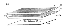
従って、図9に示されるアンテナでは、次のものを備える。
−単一給電線11を使用するプレート・プローブ10a
−平面電磁反射器30aを形成する金属プレート
−図6に示されるのと同じ、平面反射器30と接触してキャビティ21aを形成する平らな層、および
−キャビティ21aを形成する平らな層と接触する構造22
この構造は、二次元の周期性を有する。すなわち、2つの同一の重ねられた層32および34に配列された円筒形のバー25を備える。各層32および34において、バー25は相互に平行に伸び、規則正しい間隔で配列される。
従って、キャビティ21aおよび構造22から成るアセンブリ20は、平面反射器30aおよび層32および34に直交する方向の次元でその周期性に欠落部を有する。これに対して、各層32および34におけるバー25の周期的配列はキャビティ21aの存在に影響を受けない。
さらに、このアンテナの寸法は、設計動作周波数に依存する。例えば、4.75GHzの周波数で動作するためには、アンテナの横寸法は258mm、キャビティ21aの厚みは33.54mm、2つの層32および34の間隔は22.36mm、各層におけるバー25の直径は10.6mm、そのそれぞれの軸の間隔は22.36mmである。
バーは、誘電材、磁気材または金属材で構成することができる。
以上の条件の下で、図9に示されるアンテナは、図6に示されるものと同様、図8に示される通りの放射図を示す。
その代わりに、アンテナは異なるタイプの複数のプローブを持つことができる。
本発明に従ったアンテナは、以下のものとして使用できる。
−多層めっき技術によって高周波数で動作できることにより、高ビット伝送速度の高周波数アンテナ
−コンパクトなサイズでありその通過帯域が狭いため忍び込ませやすいため、宇宙または軍事用の搭載アプリケーション用のアンテナ
−椀形またはレンズ式の既知のアパーチャを有するアンテナを交換するための従来のアパーチャのアンテナ
Therefore, the antenna shown in FIG. 9 includes the following.
A
A metal plate forming the planar
This structure has a two-dimensional periodicity. That is, it comprises a
Thus, the
Further, the dimensions of the antenna depend on the design operating frequency. For example, to operate at a frequency of 4.75 GHz, the lateral dimensions of the antenna are 258 mm, the thickness of the
The bar can be composed of a dielectric, magnetic or metal material.
Under the above conditions, the antenna shown in FIG. 9 shows a radiation diagram as shown in FIG. 8, like the antenna shown in FIG.
Alternatively, the antenna can have multiple probes of different types.
The antenna according to the invention can be used as:
-High frequency antenna with high bit transmission rate by being able to operate at high frequency by multilayer plating technology-Antenna for space or military on-board applications because of its compact size and narrow passband, which makes it easy to penetrate-Bowl shape Or antenna of conventional aperture for replacing antenna with known aperture of lens type
10…プローブ
20…アセンブリ
21…キャビティ
22…光子禁止帯
30…電磁反射面
Claims (13)
電気エネルギーを電磁エネルギーにおよびその逆に変換することができる少なくとも1つのプローブ(10)と、
誘電率および/または透磁率および/または導電率が異なる少なくとも2つの材料で作られるエレメントのアセンブリ(20)であって、この中に前記プローブが配置され、前記アセンブリにおける前記エレメントの配列が、前記プローブによって生成または受信される電磁波の放射および空間周波数フィルタリングを保証し、前記フィルタリングにより、特にある非送信周波数バンドにおけるギャップ内において前記アンテナの1つまたはそれ以上の送信されるべき動作周波数(f)が許容されアセンブリと、を備え、
前記エレメントのアセンブリ(20)が、放射状の周期性、および前記放射状の周期性において少なくとも1つの欠落部(21)を有するアンテナ。 An antenna, wherein the antenna comprises:
At least one probe (10) capable of converting electrical energy to electromagnetic energy and vice versa;
An assembly (20) of elements made of at least two materials having different dielectric constants and / or magnetic permeability and / or conductivity, wherein said probe is disposed therein, and said arrangement of said elements in said assembly comprises: Guaranteeing the radiation and spatial frequency filtering of the electromagnetic waves generated or received by the probe, whereby said filtering one or more operating frequencies (f) of said antenna to be transmitted, especially in gaps in certain non-transmitting frequency bands With an acceptable assembly,
An antenna wherein said element assembly (20) has a radial periodicity and at least one missing portion (21) in said radial periodicity.
前記構造が放射状の周期性を有することを特徴とする請求項1に記載のアンテナ。 The assembly of elements (20) comprises a first material of a given permittivity, permeability and conductivity forming at least one cavity (21; 21a) and its permittivity and / or permeability and / or Or a structure (22) composed of two materials having different electrical conductivity (23, 24; 25, 26; 27, 28; 23a, 23b, 24a),
The antenna according to claim 1, wherein the structure has a radial periodicity.
前記第1の層が、その誘電率および/または透磁率および/または導電率の異なる材料の連続する円筒形の層(23a、23b、24a)と接触し、同軸円筒形の前記構造を形成するために少なくとも一次元の周期パターンで配列される請求項3に記載のアンテナ。 The element assembly comprises a first cylindrical layer made of a first material (21a) forming at least one cavity in which the probe is disposed;
The first layer is in contact with a continuous cylindrical layer (23a, 23b, 24a) of a material having a different dielectric constant and / or magnetic permeability and / or conductivity to form the coaxial cylindrical structure; 4. The antenna according to claim 3, wherein the antenna is arranged in at least a one-dimensional periodic pattern.
Applications Claiming Priority (2)
| Application Number | Priority Date | Filing Date | Title |
|---|---|---|---|
| FR99/14521 | 1999-11-18 | ||
| FR9914521A FR2801428B1 (en) | 1999-11-18 | 1999-11-18 | ANTENNA PROVIDED WITH AN ASSEMBLY OF FILTER MATERIALS |
Related Parent Applications (1)
| Application Number | Title | Priority Date | Filing Date |
|---|---|---|---|
| JP2001537822A Division JP4727884B2 (en) | 1999-11-18 | 2000-11-17 | Antenna with filtering material assembly |
Publications (2)
| Publication Number | Publication Date |
|---|---|
| JP2004159372A true JP2004159372A (en) | 2004-06-03 |
| JP4714417B2 JP4714417B2 (en) | 2011-06-29 |
Family
ID=9552269
Family Applications (2)
| Application Number | Title | Priority Date | Filing Date |
|---|---|---|---|
| JP2001537822A Expired - Lifetime JP4727884B2 (en) | 1999-11-18 | 2000-11-17 | Antenna with filtering material assembly |
| JP2004051839A Expired - Lifetime JP4714417B2 (en) | 1999-11-18 | 2004-02-26 | antenna |
Family Applications Before (1)
| Application Number | Title | Priority Date | Filing Date |
|---|---|---|---|
| JP2001537822A Expired - Lifetime JP4727884B2 (en) | 1999-11-18 | 2000-11-17 | Antenna with filtering material assembly |
Country Status (11)
| Country | Link |
|---|---|
| US (1) | US6549172B1 (en) |
| EP (2) | EP1145379B1 (en) |
| JP (2) | JP4727884B2 (en) |
| CN (2) | CN100424930C (en) |
| AT (2) | ATE336091T1 (en) |
| AU (1) | AU1868401A (en) |
| CA (1) | CA2360432C (en) |
| DE (2) | DE60036195T2 (en) |
| ES (2) | ES2269897T3 (en) |
| FR (1) | FR2801428B1 (en) |
| WO (1) | WO2001037373A1 (en) |
Cited By (3)
| Publication number | Priority date | Publication date | Assignee | Title |
|---|---|---|---|---|
| JP2010504674A (en) * | 2006-09-25 | 2010-02-12 | サントル ナシオナル デチュード スパシアル | ANTENNA USING PBG (PHOTONIC BAND GAP) MATERIAL, AND SYSTEM AND METHOD USING THIS ANTENNA |
| JP2015005929A (en) * | 2013-06-21 | 2015-01-08 | 日本電信電話株式会社 | Reflector plate and antenna device |
| JP2021040244A (en) * | 2019-09-03 | 2021-03-11 | 日本電信電話株式会社 | Antenna system |
Families Citing this family (22)
| Publication number | Priority date | Publication date | Assignee | Title |
|---|---|---|---|---|
| FR2801428B1 (en) * | 1999-11-18 | 2004-10-15 | Centre Nat Rech Scient | ANTENNA PROVIDED WITH AN ASSEMBLY OF FILTER MATERIALS |
| FR2830131B1 (en) * | 2001-09-24 | 2005-06-24 | Centre Nat Rech Scient | BROADBAND OR MULTI-BAND ANTENNA |
| GB0126737D0 (en) * | 2001-11-07 | 2002-01-02 | Univ Glasgow | Filter |
| FR2843238B1 (en) | 2002-07-31 | 2006-07-21 | Cit Alcatel | MULTISOURCES ANTENNA, IN PARTICULAR FOR A REFLECTOR SYSTEM |
| US7411564B2 (en) | 2002-10-24 | 2008-08-12 | Centre National De La Recherche Scientifique (C.N.R.S.) | Frequency multiband antenna with photonic bandgap material |
| FR2854735B1 (en) * | 2003-07-31 | 2006-07-21 | Centre Nat Rech Scient | MULTI-BEAM BEEP MATERIAL ANTENNA |
| JP4181172B2 (en) | 2002-10-24 | 2008-11-12 | サントル ナシオナル ドゥ ラ ルシェルシェサイアンティフィク(セエヌエールエス) | Multi-beam antenna with photonic band gap material |
| DE60305056T2 (en) | 2002-10-24 | 2006-12-07 | Centre National De La Recherche Scientifique (C.N.R.S.) | MULTI-STREAM LENS WITH PHOTONIC BELT MATERIAL |
| FR2854734B1 (en) * | 2003-07-31 | 2006-07-21 | Centre Nat Rech Scient | ELECTROMAGNETIC WAVE EMISSION AND RECEPTION SYSTEM EQUIPPED WITH A BEAM MATERIAL MULTI-BEAM ANTENNA |
| FR2854738B1 (en) * | 2003-07-31 | 2005-08-26 | Centre Nat Rech Scient | AERIAL EQUIPMENT BIP MULTI-BAND FREQUENCY |
| FR2854737A1 (en) * | 2002-10-24 | 2004-11-12 | Centre Nat Rech Scient | Earth communications geostationary satellite multiple beam antenna having focal point radiation pattern and photonic band gap material outer surface with periodicity default providing narrow pass band |
| FR2870642B1 (en) * | 2004-05-19 | 2008-11-14 | Centre Nat Rech Scient Cnrse | BIP MATERIAL ANTENNA (PHOTONIC PROHIBITED BAND) WITH A SIDE WALL SURROUNDING A AXIS |
| JP2007235460A (en) * | 2006-02-28 | 2007-09-13 | Mitsumi Electric Co Ltd | Antenna system |
| JP4912716B2 (en) * | 2006-03-29 | 2012-04-11 | 新光電気工業株式会社 | Wiring substrate manufacturing method and semiconductor device manufacturing method |
| FR2914506B1 (en) * | 2007-03-29 | 2010-09-17 | Centre Nat Rech Scient | RESONATOR ANTENNA EQUIPPED WITH A FILTER COATING AND SYSTEM INCORPORATING THIS ANTENNA. |
| GB2456556A (en) * | 2008-01-21 | 2009-07-22 | Zarlink Semiconductor Ltd | Antenna arrangement including dielectric and ferrite materials. |
| JP4623105B2 (en) * | 2008-02-18 | 2011-02-02 | ミツミ電機株式会社 | Broadcast receiving antenna device |
| CN102113173A (en) * | 2008-07-18 | 2011-06-29 | 株式会社Emw | Antenna with complex structure of periodic, grating arrangement of dielectric and magnetic substances |
| JP5833743B2 (en) | 2011-05-06 | 2015-12-16 | タイム・リバーサル・コミュニケーションズ | Device for transmitting and receiving waves, system comprising the device, and use of such a device |
| FR2985096B1 (en) | 2011-12-21 | 2014-01-24 | Centre Nat Rech Scient | ELEMENTARY ANTENNA AND CORRESPONDING TWO-DIMENSIONAL NETWORK ANTENNA |
| RU2562401C2 (en) * | 2013-03-20 | 2015-09-10 | Александр Метталинович Тишин | Low-frequency antenna |
| GB2512083B (en) * | 2013-03-19 | 2016-10-26 | Mettalinovich Tishin Alexandr | Antenna, array or system with a material structure surrounding at least part of an antenna element |
Citations (2)
| Publication number | Priority date | Publication date | Assignee | Title |
|---|---|---|---|---|
| US5739796A (en) * | 1995-10-30 | 1998-04-14 | The United States Of America As Represented By The Secretary Of The Army | Ultra-wideband photonic band gap crystal having selectable and controllable bad gaps and methods for achieving photonic band gaps |
| JP2003514476A (en) * | 1999-11-18 | 2003-04-15 | サントル ナシオナル ドゥ ラ ルシェルシェサイアンティフィク(セエヌエールエス) | Antenna with filtering material assembly |
Family Cites Families (12)
| Publication number | Priority date | Publication date | Assignee | Title |
|---|---|---|---|---|
| US3331073A (en) * | 1965-07-01 | 1967-07-11 | Armstrong Cork Co | Antenna |
| GB1555756A (en) * | 1975-03-18 | 1979-11-14 | Aerialite Aerials Ltd | Aerials |
| US4755820A (en) * | 1985-08-08 | 1988-07-05 | The Secretary Of State For Defence In Her Britannic Majesty's Government Of The United Kingdom Of Great Britain And Northern Ireland | Antenna device |
| US5398037A (en) * | 1988-10-07 | 1995-03-14 | The Trustees Of The University Of Pennsylvania | Radomes using chiral materials |
| US5187461A (en) * | 1991-02-15 | 1993-02-16 | Karl Brommer | Low-loss dielectric resonator having a lattice structure with a resonant defect |
| US5386215A (en) * | 1992-11-20 | 1995-01-31 | Massachusetts Institute Of Technology | Highly efficient planar antenna on a periodic dielectric structure |
| US5528254A (en) * | 1994-05-31 | 1996-06-18 | Motorola, Inc. | Antenna and method for forming same |
| US5541613A (en) * | 1994-11-03 | 1996-07-30 | Hughes Aircraft Company, Hughes Electronics | Efficient broadband antenna system using photonic bandgap crystals |
| WO1996029621A1 (en) * | 1995-03-17 | 1996-09-26 | Massachusetts Institute Of Technology | Metallodielectric photonic crystal |
| US5600342A (en) * | 1995-04-04 | 1997-02-04 | Hughes Aircraft Company | Diamond lattice void structure for wideband antenna systems |
| US5614919A (en) * | 1995-04-04 | 1997-03-25 | Hughes Aircraft Company | Wire diamond lattice structure for phased array side lobe suppression and fabrication method |
| JP3158963B2 (en) * | 1995-05-31 | 2001-04-23 | 株式会社村田製作所 | Antenna duplexer |
-
1999
- 1999-11-18 FR FR9914521A patent/FR2801428B1/en not_active Expired - Fee Related
-
2000
- 2000-11-17 EP EP00981432A patent/EP1145379B1/en not_active Expired - Lifetime
- 2000-11-17 ES ES03027264T patent/ES2269897T3/en not_active Expired - Lifetime
- 2000-11-17 EP EP03027264A patent/EP1416586B1/en not_active Expired - Lifetime
- 2000-11-17 AT AT03027264T patent/ATE336091T1/en not_active IP Right Cessation
- 2000-11-17 DE DE60036195T patent/DE60036195T2/en not_active Expired - Lifetime
- 2000-11-17 ES ES00981432T patent/ES2292491T3/en not_active Expired - Lifetime
- 2000-11-17 CN CNB2003101131825A patent/CN100424930C/en not_active Expired - Fee Related
- 2000-11-17 DE DE60030013T patent/DE60030013T2/en not_active Expired - Lifetime
- 2000-11-17 AT AT00981432T patent/ATE371964T1/en not_active IP Right Cessation
- 2000-11-17 WO PCT/FR2000/003205 patent/WO2001037373A1/en active IP Right Grant
- 2000-11-17 AU AU18684/01A patent/AU1868401A/en not_active Abandoned
- 2000-11-17 CN CN00802850.8A patent/CN1203579C/en not_active Expired - Fee Related
- 2000-11-17 US US09/889,517 patent/US6549172B1/en not_active Expired - Lifetime
- 2000-11-17 JP JP2001537822A patent/JP4727884B2/en not_active Expired - Lifetime
- 2000-11-17 CA CA002360432A patent/CA2360432C/en not_active Expired - Lifetime
-
2004
- 2004-02-26 JP JP2004051839A patent/JP4714417B2/en not_active Expired - Lifetime
Patent Citations (2)
| Publication number | Priority date | Publication date | Assignee | Title |
|---|---|---|---|---|
| US5739796A (en) * | 1995-10-30 | 1998-04-14 | The United States Of America As Represented By The Secretary Of The Army | Ultra-wideband photonic band gap crystal having selectable and controllable bad gaps and methods for achieving photonic band gaps |
| JP2003514476A (en) * | 1999-11-18 | 2003-04-15 | サントル ナシオナル ドゥ ラ ルシェルシェサイアンティフィク(セエヌエールエス) | Antenna with filtering material assembly |
Cited By (4)
| Publication number | Priority date | Publication date | Assignee | Title |
|---|---|---|---|---|
| JP2010504674A (en) * | 2006-09-25 | 2010-02-12 | サントル ナシオナル デチュード スパシアル | ANTENNA USING PBG (PHOTONIC BAND GAP) MATERIAL, AND SYSTEM AND METHOD USING THIS ANTENNA |
| JP2015005929A (en) * | 2013-06-21 | 2015-01-08 | 日本電信電話株式会社 | Reflector plate and antenna device |
| JP2021040244A (en) * | 2019-09-03 | 2021-03-11 | 日本電信電話株式会社 | Antenna system |
| JP7193805B2 (en) | 2019-09-03 | 2022-12-21 | 日本電信電話株式会社 | antenna system |
Also Published As
| Publication number | Publication date |
|---|---|
| CN1203579C (en) | 2005-05-25 |
| JP4714417B2 (en) | 2011-06-29 |
| ATE336091T1 (en) | 2006-09-15 |
| AU1868401A (en) | 2001-05-30 |
| ES2292491T3 (en) | 2008-03-16 |
| US6549172B1 (en) | 2003-04-15 |
| DE60030013D1 (en) | 2006-09-21 |
| CN1519988A (en) | 2004-08-11 |
| DE60036195T2 (en) | 2008-05-15 |
| DE60030013T2 (en) | 2007-02-22 |
| EP1145379A1 (en) | 2001-10-17 |
| CN1337078A (en) | 2002-02-20 |
| JP2003514476A (en) | 2003-04-15 |
| CN100424930C (en) | 2008-10-08 |
| CA2360432A1 (en) | 2001-05-25 |
| FR2801428A1 (en) | 2001-05-25 |
| ES2269897T3 (en) | 2007-04-01 |
| EP1416586A1 (en) | 2004-05-06 |
| WO2001037373A1 (en) | 2001-05-25 |
| EP1416586B1 (en) | 2006-08-09 |
| FR2801428B1 (en) | 2004-10-15 |
| JP4727884B2 (en) | 2011-07-20 |
| CA2360432C (en) | 2008-10-07 |
| ATE371964T1 (en) | 2007-09-15 |
| DE60036195D1 (en) | 2007-10-11 |
| EP1145379B1 (en) | 2007-08-29 |
Similar Documents
| Publication | Publication Date | Title |
|---|---|---|
| JP4727884B2 (en) | Antenna with filtering material assembly | |
| Wang et al. | Metantenna: When metasurface meets antenna again | |
| Hashmi et al. | Wideband high-gain EBG resonator antennas with small footprints and all-dielectric superstructures | |
| Juyal et al. | A high-gain single-feed dual-mode microstrip disc radiator | |
| JP4428864B2 (en) | Coaxial cavity antenna | |
| Mantash et al. | CP antenna array with switching-beam capability using electromagnetic periodic structures for 5G applications | |
| CN105870637A (en) | Radial line dielectric resonant antenna array | |
| Borazjani et al. | Design and fabrication of a new high gain multilayer negative refractive index metamaterial antenna for X‐band applications | |
| WO2014148954A4 (en) | Low-frequency antenna | |
| Al-Alem et al. | Highly efficient unpackaged 60 GHz planar antenna array | |
| Mohamad et al. | Selective high impedance surface active region loading of Archimedean spiral antenna | |
| Nahar et al. | Efficiency enhancement techniques of microwave and millimeter‐wave antennas for 5G communication: A survey | |
| Vaidya et al. | Efficient, high gain with low side lobe level antenna structures using parasitic patches on multilayer superstrate | |
| Ratni et al. | Low‐profile circularly polarized fabry–perot cavity antenna | |
| Xue et al. | An ultrathin dual-band Huygens’ meta-lens antenna with orthogonal linear polarization | |
| Zhiming et al. | Investigations and prospects of Fabry-Perot antennas: A review | |
| US8253641B1 (en) | Wideband wide scan antenna matching structure using electrically floating plates | |
| Guthi et al. | High gain and wideband circularly polarized S‐shaped patch antenna with reactive impedance surface and frequency‐selective surface configuration for Wi‐Fi and Wi‐Max applications | |
| JP2004208285A (en) | Mutual coaxial type colinear antenna | |
| Wang et al. | A TE₀₁-mode groove-gap-waveguide-based wideband fixed-frequency beam-scanning leaky-wave antenna for millimeter-wave applications | |
| Boukern et al. | High‐gain cavity antenna combining AMC‐reflector and FSS superstrate technique | |
| Hashmi et al. | Achieving high directivity-bandwidth through flat GRIN superstrates in Fabry-Perot cavity antennas | |
| Attia et al. | Reduction of grating lobes for slot antenna array at 60 GHz using multilayer spatial angular filter | |
| CN114421176A (en) | Electromagnetic lens based on artificial dielectric material | |
| Zhang et al. | Research progress on millimeter wave transmitarray in SKLMMW |
Legal Events
| Date | Code | Title | Description |
|---|---|---|---|
| A621 | Written request for application examination |
Free format text: JAPANESE INTERMEDIATE CODE: A621 Effective date: 20070925 |
|
| A131 | Notification of reasons for refusal |
Free format text: JAPANESE INTERMEDIATE CODE: A131 Effective date: 20100209 |
|
| A601 | Written request for extension of time |
Free format text: JAPANESE INTERMEDIATE CODE: A601 Effective date: 20100507 |
|
| A602 | Written permission of extension of time |
Free format text: JAPANESE INTERMEDIATE CODE: A602 Effective date: 20100512 |
|
| A521 | Request for written amendment filed |
Free format text: JAPANESE INTERMEDIATE CODE: A523 Effective date: 20100809 |
|
| A131 | Notification of reasons for refusal |
Free format text: JAPANESE INTERMEDIATE CODE: A131 Effective date: 20100831 |
|
| A601 | Written request for extension of time |
Free format text: JAPANESE INTERMEDIATE CODE: A601 Effective date: 20101129 |
|
| A602 | Written permission of extension of time |
Free format text: JAPANESE INTERMEDIATE CODE: A602 Effective date: 20101202 |
|
| A521 | Request for written amendment filed |
Free format text: JAPANESE INTERMEDIATE CODE: A523 Effective date: 20110218 |
|
| A01 | Written decision to grant a patent or to grant a registration (utility model) |
Free format text: JAPANESE INTERMEDIATE CODE: A01 Effective date: 20110308 |
|
| A61 | First payment of annual fees (during grant procedure) |
Free format text: JAPANESE INTERMEDIATE CODE: A61 Effective date: 20110328 |
|
| R250 | Receipt of annual fees |
Free format text: JAPANESE INTERMEDIATE CODE: R250 |
|
| R250 | Receipt of annual fees |
Free format text: JAPANESE INTERMEDIATE CODE: R250 |
|
| R250 | Receipt of annual fees |
Free format text: JAPANESE INTERMEDIATE CODE: R250 |
|
| R250 | Receipt of annual fees |
Free format text: JAPANESE INTERMEDIATE CODE: R250 |
|
| R250 | Receipt of annual fees |
Free format text: JAPANESE INTERMEDIATE CODE: R250 |
|
| R250 | Receipt of annual fees |
Free format text: JAPANESE INTERMEDIATE CODE: R250 |