JP2004158564A - Laser doping method and thin film transistor manufacturing method - Google Patents
Laser doping method and thin film transistor manufacturing method Download PDFInfo
- Publication number
- JP2004158564A JP2004158564A JP2002321619A JP2002321619A JP2004158564A JP 2004158564 A JP2004158564 A JP 2004158564A JP 2002321619 A JP2002321619 A JP 2002321619A JP 2002321619 A JP2002321619 A JP 2002321619A JP 2004158564 A JP2004158564 A JP 2004158564A
- Authority
- JP
- Japan
- Prior art keywords
- film
- dopant
- laser
- semiconductor layer
- doping
- Prior art date
- Legal status (The legal status is an assumption and is not a legal conclusion. Google has not performed a legal analysis and makes no representation as to the accuracy of the status listed.)
- Granted
Links
Images
Classifications
-
- H—ELECTRICITY
- H10—SEMICONDUCTOR DEVICES; ELECTRIC SOLID-STATE DEVICES NOT OTHERWISE PROVIDED FOR
- H10D—INORGANIC ELECTRIC SEMICONDUCTOR DEVICES
- H10D86/00—Integrated devices formed in or on insulating or conducting substrates, e.g. formed in silicon-on-insulator [SOI] substrates or on stainless steel or glass substrates
-
- H—ELECTRICITY
- H10—SEMICONDUCTOR DEVICES; ELECTRIC SOLID-STATE DEVICES NOT OTHERWISE PROVIDED FOR
- H10D—INORGANIC ELECTRIC SEMICONDUCTOR DEVICES
- H10D30/00—Field-effect transistors [FET]
- H10D30/01—Manufacture or treatment
- H10D30/021—Manufacture or treatment of FETs having insulated gates [IGFET]
- H10D30/031—Manufacture or treatment of FETs having insulated gates [IGFET] of thin-film transistors [TFT]
- H10D30/0312—Manufacture or treatment of FETs having insulated gates [IGFET] of thin-film transistors [TFT] characterised by the gate electrodes
- H10D30/0314—Manufacture or treatment of FETs having insulated gates [IGFET] of thin-film transistors [TFT] characterised by the gate electrodes of lateral top-gate TFTs comprising only a single gate
-
- H—ELECTRICITY
- H10—SEMICONDUCTOR DEVICES; ELECTRIC SOLID-STATE DEVICES NOT OTHERWISE PROVIDED FOR
- H10D—INORGANIC ELECTRIC SEMICONDUCTOR DEVICES
- H10D30/00—Field-effect transistors [FET]
- H10D30/01—Manufacture or treatment
- H10D30/021—Manufacture or treatment of FETs having insulated gates [IGFET]
- H10D30/031—Manufacture or treatment of FETs having insulated gates [IGFET] of thin-film transistors [TFT]
- H10D30/0321—Manufacture or treatment of FETs having insulated gates [IGFET] of thin-film transistors [TFT] comprising silicon, e.g. amorphous silicon or polysilicon
-
- H—ELECTRICITY
- H10—SEMICONDUCTOR DEVICES; ELECTRIC SOLID-STATE DEVICES NOT OTHERWISE PROVIDED FOR
- H10D—INORGANIC ELECTRIC SEMICONDUCTOR DEVICES
- H10D86/00—Integrated devices formed in or on insulating or conducting substrates, e.g. formed in silicon-on-insulator [SOI] substrates or on stainless steel or glass substrates
- H10D86/01—Manufacture or treatment
- H10D86/021—Manufacture or treatment of multiple TFTs
- H10D86/0221—Manufacture or treatment of multiple TFTs comprising manufacture, treatment or patterning of TFT semiconductor bodies
- H10D86/0223—Manufacture or treatment of multiple TFTs comprising manufacture, treatment or patterning of TFT semiconductor bodies comprising crystallisation of amorphous, microcrystalline or polycrystalline semiconductor materials
- H10D86/0225—Manufacture or treatment of multiple TFTs comprising manufacture, treatment or patterning of TFT semiconductor bodies comprising crystallisation of amorphous, microcrystalline or polycrystalline semiconductor materials using crystallisation-promoting species, e.g. using a Ni catalyst
-
- H—ELECTRICITY
- H10—SEMICONDUCTOR DEVICES; ELECTRIC SOLID-STATE DEVICES NOT OTHERWISE PROVIDED FOR
- H10P—GENERIC PROCESSES OR APPARATUS FOR THE MANUFACTURE OR TREATMENT OF DEVICES COVERED BY CLASS H10
- H10P32/00—Diffusion of dopants within, into or out of wafers, substrates or parts of devices
- H10P32/10—Diffusion of dopants within, into or out of semiconductor bodies or layers
- H10P32/14—Diffusion of dopants within, into or out of semiconductor bodies or layers within a single semiconductor body or layer in a solid phase; between different semiconductor bodies or layers, both in a solid phase
- H10P32/1408—Diffusion of dopants within, into or out of semiconductor bodies or layers within a single semiconductor body or layer in a solid phase; between different semiconductor bodies or layers, both in a solid phase from or through or into an external applied layer, e.g. photoresist or nitride layers
- H10P32/141—Diffusion of dopants within, into or out of semiconductor bodies or layers within a single semiconductor body or layer in a solid phase; between different semiconductor bodies or layers, both in a solid phase from or through or into an external applied layer, e.g. photoresist or nitride layers the applied layer comprising oxides only
-
- H—ELECTRICITY
- H10—SEMICONDUCTOR DEVICES; ELECTRIC SOLID-STATE DEVICES NOT OTHERWISE PROVIDED FOR
- H10P—GENERIC PROCESSES OR APPARATUS FOR THE MANUFACTURE OR TREATMENT OF DEVICES COVERED BY CLASS H10
- H10P32/00—Diffusion of dopants within, into or out of wafers, substrates or parts of devices
- H10P32/10—Diffusion of dopants within, into or out of semiconductor bodies or layers
- H10P32/17—Diffusion of dopants within, into or out of semiconductor bodies or layers characterised by the semiconductor material
- H10P32/171—Diffusion of dopants within, into or out of semiconductor bodies or layers characterised by the semiconductor material being group IV material
-
- H—ELECTRICITY
- H10—SEMICONDUCTOR DEVICES; ELECTRIC SOLID-STATE DEVICES NOT OTHERWISE PROVIDED FOR
- H10P—GENERIC PROCESSES OR APPARATUS FOR THE MANUFACTURE OR TREATMENT OF DEVICES COVERED BY CLASS H10
- H10P34/00—Irradiation with electromagnetic or particle radiation of wafers, substrates or parts of devices
- H10P34/40—Irradiation with electromagnetic or particle radiation of wafers, substrates or parts of devices with high-energy radiation
- H10P34/42—Irradiation with electromagnetic or particle radiation of wafers, substrates or parts of devices with high-energy radiation with electromagnetic radiation, e.g. laser annealing
-
- H—ELECTRICITY
- H10—SEMICONDUCTOR DEVICES; ELECTRIC SOLID-STATE DEVICES NOT OTHERWISE PROVIDED FOR
- H10P—GENERIC PROCESSES OR APPARATUS FOR THE MANUFACTURE OR TREATMENT OF DEVICES COVERED BY CLASS H10
- H10P14/00—Formation of materials, e.g. in the shape of layers or pillars
- H10P14/20—Formation of materials, e.g. in the shape of layers or pillars of semiconductor materials
- H10P14/29—Formation of materials, e.g. in the shape of layers or pillars of semiconductor materials characterised by the substrates
- H10P14/2901—Materials
-
- H—ELECTRICITY
- H10—SEMICONDUCTOR DEVICES; ELECTRIC SOLID-STATE DEVICES NOT OTHERWISE PROVIDED FOR
- H10P—GENERIC PROCESSES OR APPARATUS FOR THE MANUFACTURE OR TREATMENT OF DEVICES COVERED BY CLASS H10
- H10P14/00—Formation of materials, e.g. in the shape of layers or pillars
- H10P14/20—Formation of materials, e.g. in the shape of layers or pillars of semiconductor materials
- H10P14/34—Deposited materials, e.g. layers
- H10P14/3402—Deposited materials, e.g. layers characterised by the chemical composition
- H10P14/3404—Deposited materials, e.g. layers characterised by the chemical composition being Group IVA materials
- H10P14/3411—Silicon, silicon germanium or germanium
-
- H—ELECTRICITY
- H10—SEMICONDUCTOR DEVICES; ELECTRIC SOLID-STATE DEVICES NOT OTHERWISE PROVIDED FOR
- H10P—GENERIC PROCESSES OR APPARATUS FOR THE MANUFACTURE OR TREATMENT OF DEVICES COVERED BY CLASS H10
- H10P14/00—Formation of materials, e.g. in the shape of layers or pillars
- H10P14/20—Formation of materials, e.g. in the shape of layers or pillars of semiconductor materials
- H10P14/38—Formation of materials, e.g. in the shape of layers or pillars of semiconductor materials characterised by treatments done after the formation of the materials
- H10P14/3802—Crystallisation or recrystallisation of non-monocrystalline semiconductor materials, e.g. regrowth
- H10P14/3806—Crystallisation or recrystallisation of non-monocrystalline semiconductor materials, e.g. regrowth using crystallisation-enhancing elements
-
- H—ELECTRICITY
- H10—SEMICONDUCTOR DEVICES; ELECTRIC SOLID-STATE DEVICES NOT OTHERWISE PROVIDED FOR
- H10P—GENERIC PROCESSES OR APPARATUS FOR THE MANUFACTURE OR TREATMENT OF DEVICES COVERED BY CLASS H10
- H10P14/00—Formation of materials, e.g. in the shape of layers or pillars
- H10P14/20—Formation of materials, e.g. in the shape of layers or pillars of semiconductor materials
- H10P14/38—Formation of materials, e.g. in the shape of layers or pillars of semiconductor materials characterised by treatments done after the formation of the materials
- H10P14/3802—Crystallisation or recrystallisation of non-monocrystalline semiconductor materials, e.g. regrowth
- H10P14/3808—Crystallisation or recrystallisation of non-monocrystalline semiconductor materials, e.g. regrowth using laser beams
Landscapes
- Recrystallisation Techniques (AREA)
- Thin Film Transistor (AREA)
Abstract
【課題】濃度制御が容易であり、かつ、大面積に対するドーピングを実用的に行うことができ、さらに、特殊な装置を必要としない簡便なドーピング方法を提供することを課題とする。
【手段】本発明ではドーパントを含む液体を、ドーピングを行う半導体の表面に塗布してから、該半導体の表面にレーザー光を照射することでドーパントを該半導体に添加するレーザードーピング処理方法を提案する。また、同時に結晶化も行うことが可能である。
【選択図】 図1An object of the present invention is to provide a simple doping method that can easily perform concentration control, can practically perform doping over a large area, and does not require a special device.
The present invention proposes a laser doping method in which a liquid containing a dopant is applied to the surface of a semiconductor to be doped and then the surface of the semiconductor is irradiated with laser light to add the dopant to the semiconductor. . Further, crystallization can be performed at the same time.
[Selection diagram] Fig. 1
Description
【0001】
【発明の属する技術分野】
本発明は、半導体に不純物をドーピングする方法に関する。特にドーピングされる不純物の添加量に精密な制御が必要であるチャネルドーピングに関し、レーザー光を照射することにより半導体に不純物を添加するレーザードーピング処理方法に関する。
【0002】
【従来の技術】
半導体の電気的性質を利用し、半導体素子を作製する際にその電気的性質を制御するために、半導体に微量の不純物を添加するドーピングという技術が、現在汎用されている。半導体にドーピングをする方法は、原料より半導体を形成する過程で不純物を添加する方法と、半導体を形成してから不純物を添加する方法と、大きく2つにわけることができる。また、不純物を添加する方法として、代表的にはイオン注入法、プラズマドーピング法、レーザードーピング法などが挙げられる。
【0003】
イオン注入法はドーパントを含むガスをプラズマ室に添加することで、イオンビームを引き出し、質量分析器にかけることで所望のドーパントイオンを数keV〜数百keVのエネルギーで加速し、半導体の表面に衝突させ、物理的にドーパントを添加する方法である。また、プラズマドーピング法は、所望の濃度に希釈されたドーパントガスを含むプラズマ中に半導体をさらす、あるいは前記プラズマ中から引き出されたイオンに半導体をさらすことによりドーピングを行う方法である。プラズマドーピング法は質量分析を行わないため、プラズマ中に発生した様々な形態のイオンがドーピングされる。
【0004】
ドーピング法の一形態として、レーザードーピング法も使用されている。レーザードーピング法は、ドーパントを含むガス中に半導体を設置し、その表面にレーザー光を照射することで溶融添加、そして活性化する方法である。レーザードーピング法は広範囲のドーピング、高活性化が可能であるが、さらにその効率を上げるために試料を加熱したり、電磁エネルギーを与えながらレーザーを照射したりするなどの研究もなされている(例えば、特許文献1参照)。
【0005】
一方、半導体の世界は、日進月歩の勢いで高速化、微細化が進んでいる。それに伴い、半導体そのものや、回路の信頼性向上が強く求められている。半導体素子を評価する一パラメータとしてしきい値電圧が良く用いられるが、しきい値電圧は高すぎても低すぎても信頼性に欠け、所望のしきい値電圧を得られることが最も重要である。
【0006】
このしきい値電圧を制御するための手段としてチャネルドーピングという技術が用いられている。チャネルドーピングとは、その名のとおり、チャネル形成領域となる部分に、所望のしきい値電圧を得られるように極微量の不純物を添加する技術である。チャネルドーピングは精密にしきい値電圧の変化を制御することが目的であるため、その添加量を精密に制御することが必要となる。
【0007】
イオン注入法またはプラズマドーピング法におけるイオンの注入量の制御は、流れるイオンを電流として計測するファラデーカップ電流計を用いて制御している。必要な種類のイオンのみをドーピングすることができるイオン注入法は、精密な濃度制御が必要なチャネルドーピングには好適に使用することができる。
【0008】
また、高速化、微細化を実現するためには、ゲート長を短くすることも必要になってくる。しかし、ゲート長を短くすると、チャネル形成領域の深い部分で電流がもれてしまう、所謂短チャネル効果が発生し、問題となっている。これを防ぐためにはソース領域及びドレイン領域の極浅い部分にのみ不純物を添加すること(浅い接合を形成すること)が有効である。
【0009】
ところで、ガラス基板など、耐熱性の低い基板に対して結晶質の半導体層を形成する技術として、Niに代表される結晶化を助長する元素を用いる技術がある。ガラス基板上にアモルファスシリコンを形成し、Niを含む溶液をスピナーにより塗布、またはスパッタリングなどでNiの薄い膜を形成した後、結晶化を行うことで、低温、短時間で結晶化が行われるという技術である。この技術は安価なガラス基板を用いることで、製品の価格を下げるために無くてはならない重要な技術である。
【0010】
【特許文献1】
特開平5−326430号公報
【0011】
【発明が解決しようとする課題】
ドーピングの問題として、年々高集積化してゆく回路、そして大型化して行くディスプレイに伴い、製造工程に流れる基板サイズが大型化して、ドーピングが必要な領域も拡大している現状が挙げられる。
【0012】
イオン注入法はイオンビームを正確に質量分離させるために、ビームを細くすることが必要である。そのため、一度に広範囲にわたってドーピングを行うことができず、処理に膨大な時間がかかってしまうため、広範囲なドーピング処理に対応できないという重大な問題点がある。
【0013】
また、イオン注入法において、浅い接合を形成しようとすると、低いエネルギーでイオンを注入しなければいけないが、低いエネルギーのイオンビームは発散してしまい、十分な電流量を得ることが困難であるという問題点もある。また、イオン注入によるダメージを回復させるための熱アニールによって、ドーパントが拡散してしまい、極浅い領域にのみ不純物を添加することは非常に難しい。
【0014】
また、プラズマドーピング法においては、処理時間という点でイオン注入法より有利ではあるが、質量分離を行わないため、ファラデーカップ電流計で計測されるイオン電流は、ドーパントガスを希釈したガスのイオンとドーパントイオンを足した、トータルのイオン電流である。したがって、トータルのイオンドーピング量を正確に制御しても、ドーパントガスを希釈しているガスとドーパントのガスとの比、すなわちイオン比割合が装置稼動中に変化すると、注入ドーパント量も変化してしまう。そのため、精密な濃度制御が必要なチャネルドーピングに適用するには問題がある。
【0015】
一方、レーザードーピング法において、多く行われているドーパントガス雰囲気中でレーザー光を照射する方法では、注入するドーパント量の制御が困難であり、ドーパントを均一に分配させるために特殊な装置が必要となってしまう。
【0016】
また、別な問題として結晶化を助長する元素は、結晶化に関して非常に有利な働きをするが、結晶化後に大量に半導体層中にこれら元素が残留しているとその半導体層を用いてTFT、特にTFTのチャネル領域を作製した場合、TFTの特性に悪影響を及ぼしてしまう。そのため、これら結晶化を助長する元素を用いて結晶化を行った場合は、ゲッタリングという該元素の濃度を低減させる手段がとられることが普通である。
【0017】
ゲッタリングは、結晶化を助長させる元素が大量に残っていると不都合である領域から、他の領域(ゲッタリン領域と呼ばれる)に移動させることによって行う。
【0018】
残留Ni元素の除去に関しては、本出願人によりゲッタリング処理による方法(特開平10−214786号公報)が開示されているが、選択的にNi元素を添加するためのマスク形成工程と、ゲッタリング元素を選択的に添加するためのマスク形成工程が必要とされ、熱処理も結晶化工程とゲッタリング工程とで2回行う必要があること、などの工程増加の問題があり、生産性やコストを悪化させていた。
【0019】
これらの問題を鑑み、本発明では濃度制御が容易であり、かつ、大面積に対するドーピングを実用的に行うことができ、さらに、特殊な装置を必要としない簡便なドーピング方法を提供することを課題とする。
【0020】
また、浅い接合などに対応可能な、深さ方向の濃度制御を容易に行えるドーピング方法を提供することを課題とする。
【0021】
さらに、生産性やコストを悪化させないゲッタリング方法を提供することを課題とする。
【0022】
【課題を解決するための手段】
そこで、本発明ではドーパント(価電子制御を目的とした一導電型の不純物)を含む液体を、ドーピングを行う半導体の表面に塗布してから、該半導体の表面にレーザー光を照射することでドーパントを該半導体に添加するレーザードーピング処理方法を提案する。
【0023】
本法では、液体でドーパントを供給するために、ドーパントを含む液体中のドーパント濃度を調整することで、容易に半導体に添加するドーパントの濃度を制御することができる。そのため、しきい値電圧制御を行うために要求されるドーパント濃度の制御を好適に行うことができるようになる。
【0024】
また、レーザードーピング処理は、レーザーが照射された部分が溶融し、ドーパントが取り込まれる。そのため、レーザー光で与えるエネルギーを調節することによって、溶融する半導体の深さを調節することができるため、ドーパントを添加する深さを容易に調節することが可能となる。そのため、浅い接合を形成することも容易となる。
【0025】
また、本発明は、絶縁表面を有する基板上に形成された非晶質半導体層上にドーパントを含む液体を塗布し、レーザー光を照射することによって前記非晶質半導体層を結晶化し、結晶質半導体層とすることと同時に、前記結晶質半導体層にドーパントの添加を行うことを特徴とする。
【0026】
この構成により、レーザー光による結晶化と、ドーパントの添加を同時に行うことができるようになるため、工程の短縮、及びそれに伴うスループットの向上が期待できる。
【0027】
また、本発明は絶縁表面を有する基板上に形成された非晶質半導体層上にドーパント及び結晶化を助長する元素を含む液体を塗布し、レーザー光を照射することによって前記非晶質半導体層を結晶化し、結晶質半導体層とすることと同時に、前記結晶質半導体層にドーパントの添加を行うことを特徴とする。
【0028】
この構成により、ドーパントと同時に結晶化を助長する元素を同時に添加することができ、結晶性のよい結晶質半導体層を得ることができるうえ、その結晶化と同時にドーパントの添加を行うことができ、工程の短縮及びスループットの向上が期待できる。
【0029】
さらに、本発明は絶縁表面を有する基板上に形成された非晶質半導体層上に結晶化を助長する元素を含む液体を塗布し、前記非晶質半導体層を加熱することにより結晶化して結晶質半導体膜とし、前記結晶質半導体層上にドーパントを含む液体を塗布し、レーザー光を照射することによって前記結晶質半導体層にドーパントの添加を行うことを特徴とする。
【0030】
この構成により、結晶化を助長する元素を用いて熱結晶化を行った後のレーザーニールと同時に半導体にドーパントを添加することができ、工程の短縮につながる。
【0031】
また、本発明において、結晶化を助長する元素を用いて結晶化を行った半導体層の中には、結晶化を助長する元素が高濃度に残存している。該半導体層にドーパントを含む液体を塗布しレーザー光の照射を行うと、半導体層は溶融し、ドーパントが取り込まれるが、レーザー光の照射によって与えられた熱は基板側から放散するため、固化は基板側からはじまる。すると、ドーパントの濃度は基板から遠ざかるほど、つまり、半導体層の表面に近づくにしたがって高くなるように偏析する。結晶化を助長する元素は不純物濃度の高い方に移動しやすいため、結晶化を助長する元素の濃度も同様に表面に行くほど高くなるように偏析する。この結晶化を助長する元素濃度、ドーパント濃度が共に高い部分を、エッチングや化学的機械研磨(CMP)などによって除去することで、ゲッタリングを行うことを特徴とする。
【0032】
この構成により、工程数の大きく増加するゲッタリング法を使用しなくても、ドーピング工程にエッチングまたはCMP工程を追加するだけで、ゲッタリングを完了し、良好な特性のTFTを作製することができる結晶質半導体層を作製することができる。
【0033】
以上のような構成をとる本発明では、特別な装置を必要としなくても、より正確に添加ドーパントの濃度を制御することができ、さらに、ドーパントを添加する深さの制御が容易となり、その上、工程の短縮によりスループットが向上するといった効果を奏する。
【0034】
【実施の形態】
(実施の形態1)
本実施の形態ではドーパントを含む液体を塗布し、レーザー光を照射することで半導体へのドーピングを行う方法について説明する。
【0035】
半導体の表面に、ドーパントを含む液体をスピナーで塗布し、ドーパントを含む液体の薄い膜を形成する。ドーパントとしてはN型、またはP型を付与する元素を用い、代表的にはN型としてリン、砒素、アンチモン、P型としてボロン、アルミニウム、ガリウムなどがある。濃度は最終的に半導体膜中に所望の濃度が添加されるように液体中のドーパント濃度を調節する。
【0036】
P型、またはN型を付与する元素を含む液体としては、代表的にはおのおのホウ酸又はリン酸の水溶液などが挙げられる。半導体の表面にこれらの水溶液を塗布する場合は、半導体表面と水との濡れ性があまり良くないため、濡れ性を向上させるため、あらかじめ半導体膜の表面にオゾン水を塗布することによって極薄い酸化膜を形成しておくとよい。また、このP型またはN型を付与する元素はこれに限らず、適宜溶媒に溶解して塗布することができ、半導体の特性に重大な影響を及ぼす元素が含まれていないものであれば、使用することができる。また、溶媒も水に限らず、P型またはN型を付与する元素に合わせて有機溶媒なども使用することもできる。例えば、有機溶媒としては、ベンゼン、トルエン、キシレン、四塩化炭素、クロロホルム、エーテル、エタノールなどが使用でき、この場合は、半導体膜表面に酸化膜は形成しなくともよい。さらに、塗布する液体は溶液に限らず、均一分散液、コロイド溶液などでもよい。
【0037】
ドーパントを含む液体を塗布した後、レーザー光を照射し、ドーピングを行う。レーザー光は、パルス発振型または連続発光型の気体レーザー、固体レーザーもしくは金属レーザーを用いることができる。これらのレーザーを用いる場合には、レーザー発振器から放射されたレーザー光を光学系で線状に集光し、半導体膜に照射する方法を用いると良い。
【0038】
このレーザー照射によって、半導体の全部、又は一部が溶融し、ドーパントが取り込まれることにより半導体層中にドーパントが添加されることになる。
【0039】
このように、レーザードーピングを行うことで、半導体に精度良く所望の濃度の不純物を添加することができる、大面積基板においても信頼性の高いTFTをスループット良く得ることができる。
【0040】
(実施の形態2)
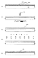
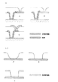
本実施の形態では結晶化とレーザードーピングを同時に行う方法について図1を用いて説明する。
【0041】
まず、基板100上に下地絶縁膜101a、101bを形成する。基板としては、ガラス基板、石英基板、結晶性ガラスなどの絶縁性基板や、セラミック基板、ステンレス基板、金属基板(タンタル、タングステン、モリブデン等)、半導体基板、プラスチック基板(ポリイミド、アクリル、ポリエチレンテレフタレート、ポリカーボネート、ポリアリレート、ポリエーテルスルホン等)等を用いることができる。これらの中より、プロセスの最高温度や、用途などを考慮して適したものを選べばよい。
【0042】
下地絶縁膜101a、101bは酸化シリコン膜、窒化シリコン膜、酸化窒化シリコン膜などの絶縁膜を単層又は2以上の複数層形成して形成する。これらはスパッタ法や減圧CVD法、プラズマCVD法等公知の方法を用いて形成する。本実施の形態では2層の積層構造としているが、もちろん単層でも3層以上の複数層でも構わない。
【0043】
次いで、非晶質半導体膜102を形成する。非晶質半導体膜はシリコンまたはシリコンを主成分とする材料(例えばSixGe1−x等)で25〜80nm(好ましくは30〜60nm)の厚さに形成すればよい。作製方法としては、公知の方法、例えばスパッタ法、減圧CVD法、またはプラズマCVD法等が使用できる。本実施の形態では、アモルファスシリコンにより膜厚50nmで形成した。(図1(A))
【0044】
続いて、ドーパントを含む液体103をスピナーで塗布し(図1(B))、非晶質半導体膜表面にドーパントを含む液体の薄い膜104を形成した(図1(C))。ドーパントとしてはN型、またはP型を付与する元素を用い、代表的にはリン、ボロンなどがある(本実施の形態ではボロン(B)をホウ酸水溶液として使用する)。なお、この場合は、非晶質半導体膜の表面に均一に塗布させるため、ホウ酸水溶液を塗布する前に、オゾン水で半導体層表面を処理することにより極薄い酸化膜(図示せず)を形成しておくとよい。
【0045】
ボロンの濃度は最終的に半導体膜中に所望のしきい値電圧を得られる程度にボロンが添加できれば良く、1×10¹⁵〜1×10¹⁸atoms/cm3(代表的には、5×1016〜5×1017atoms/cm3)位の濃度が添加されるように濃度を調節する。
【0046】
ホウ酸水溶液104を形成した後、レーザー光を照射し、ドーピングと同時に結晶化を行う。(図1(D))レーザーは、パルス発振型または連続発光型の気体レーザー、固体レーザーもしくは金属レーザーを用いることができる。これらのレーザーを用いる場合には、レーザー発振器から放射されたレーザー光を光学系で線状に集光し、半導体膜に照射する方法を用いると良い。
【0047】
気体レーザーとしては、エキシマレーザー、Arレーザー、Krレーザー、固体レーザーとして、YAGレーザー、YVO4レーザー、YLFレーザー、YAlO3レーザー、ガラスレーザー、ルビーレーザー、アレキサンドライドレーザー、Ti:サファイアレーザー、金属レーザーとしては、ヘリウムカドミウムレーザ、銅蒸気レーザー、金蒸気レーザーが挙げられる。固体レーザーは、Cr3+、Cr4+、Nd3+、Er3+、Ce3+、Co2+、Ti3+、Yb3+又はV3+がドーピングされたYAG、YVO4、YLF、YAlO3などの結晶を使ったレーザー等が使用可能である。当該レーザーの基本波はドーピングする材料によって異なり、1μm前後の基本波を有するレーザー光が得られる。基本波に対する高調波は、非線形光学素子を用いることで得ることができる。
【0048】
レーザー照射の条件は実施者が適宣選択するものであるが、エキシマレーザーを用いる場合はパルス発振周波数300Hzとし、レーザーエネルギー密度を100〜400mJ/cm2(代表的には200〜300mJ/cm2)とする。また、YAGレーザーを用いる場合にはその高次高調波を用いパルス発振周波数30〜300kHzとし、レーザーエネルギー密度を300〜600mJ/cm2(代表的には350〜500mJ/cm2))とすると良い。そして幅100〜1000μm、例えば400μmで線状に集光したレーザー光を基板全面に渡って照射し、この時の線状レーザー光の重ね合わせ率(オーバーラップ率)を50〜90%として行う。
【0049】
このレーザー光の照射によって、非晶質半導体層102の全部もしくは一部が溶融し、ボロンが取り込まれることにより非晶質半導体層102中にボロンが添加される。なお、本実施の形態では、非晶質半導体層102をパターニングする前にレーザー光の照射を行ったが、パターニングを行い、所望の形状としてから塗布及びレーザー光の照射を行っても構わない。このようにして、ボロンが導入された結晶質半導体膜105が形成される。(図1(E))
【0050】
このように、ホウ酸水溶液を塗布したのち、レーザー光を適当な条件で照射することによって、チャネルドーピングと同時に結晶化まで行うことができ、半導体に精度良く所望の濃度の不純物を添加することができる。また、結晶化の工程と同時にチャネルドーピングを行うことができるため、チャネルドーピングの工程を一部短縮することが可能となり、効率の向上が期待できる。さらに、該半導体層をチャネル形成領域としたTFTを作製することで、しきい値電圧制御が容易となり、大面積基板においても信頼性の高いTFTを更にスループット良く得ることができる。
【0051】
(実施の形態3)
本発明の他の実施の形態について、実施の形態2と同様に図1を使用して説明する。
【0052】
実施の形態2と同様に、基板100上に下地絶縁膜101a、101bを形成し、非晶質半導体層102を形成する。(図1(A))
【0053】
次に、ドーパント(ボロン)を含む液体(ホウ酸水溶液)中に同時に結晶化を助長する元素を重量換算で5〜100ppm含ませ、非晶質半導体層102上にスピナーで塗布する。本実施の形態では、重量換算で10ppmのNiに相当する酢酸ニッケルを同じにホウ酸水溶液中に含ませ、ドーパントとNiを含む液体103の薄い膜104を非晶質半導体層102の上に形成する。なお、結晶化を助長する元素とは、他に鉄(Fe)、パラジウム(Pd)、スズ(Sn)、鉛(Pb)、コバルト(Co)、白金(Pt)、銅(Cu)、金(Au)などがあるが、この中から一種または複数種を適宜使用すればよい。(図1(B)(C))
【0054】
続いて、実施の形態2と同様にレーザー光を照射する。その結果、触媒元素は溶融状態となった半導体層中を、シリサイドを形成しながら拡散し、その過程で半導体層の結晶化を促進させる効果があり、実施の形態2と比較してより結晶性の高い結晶質半導体層105を形成することを可能とする。
【0055】
また、この結晶化においてボロンも半導体層が溶融状態となることによって取り込まれ、添加される。
【0056】
このように、本実施の形態は、チャネルドーピングと同時に結晶化を助長する元素を使用した結晶化まで行うことができる。そのため、結晶化を助長する元素を用い、レーザー結晶化を行う工程において、チャネルドーピング工程数を増やさず行うことができ、効率が非常に向上することが期待できる。さらに、結晶質半導体膜に精度良く所望の濃度の不純物を添加することができ、結晶質半導体膜をチャネル形成領域としたTFTを作製することで、しきい値電圧制御が容易となり、大面積基板においても信頼性の高いTFTを更にスループット良く得ることもできるという効果がある。
【0057】
なお、本実施の形態では、非晶質半導体膜102をパターニングする前に結晶化を行ったが、パターニングを行い、所望の形状としてから塗布及び結晶化を行っても構わない。
【0058】
(実施の形態4)
本発明における他の実施の形態について、図2を使用して説明する。
【0059】
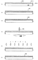
実施の形態2及び実施の形態3と同様に基板200上に、下地絶縁膜201a、201b、非晶質半導体膜202を形成する。(図2(A))
【0060】
次に、非晶質半導体膜202の結晶化を行う。本実施の形態では、触媒元素を用いた加熱による結晶化を行う。重量換算で10ppmのニッケルを含む酢酸ニッケル塩溶液をスピナーで塗布し、非晶質半導体膜202表面にニッケル溶液の薄い膜203を形成する(図2(B))。塗布に代えてスパッタ法でニッケル元素を全面に散布する方法を用いてもよい。触媒元素としては、ニッケル(Ni)以外に、鉄(Fe)、パラジウム(Pd)、スズ(Sn)、鉛(Pb)、コバルト(Co)、白金(Pt)、銅(Cu)、金(Au)、といった元素などから選んだ一種または複数種を使用してもよい。
【0061】
次いで、加熱処理を行い、非晶質半導体膜202を結晶化させる。触媒元素を用いているため、500℃〜650℃で4〜24時間程度行えばよい。この結晶化処理により、非晶質半導体膜膜202は結晶質の導体層膜204となる(図2(C))。本実施の形態では、結晶化は結晶化を助長する金属を用いた加熱による方法で行ったが、この結晶化はレーザー結晶化など、他の公知の方法を使用して行っても良い。
【0062】
続いて、実施の形態2と同様にドーパントを含む液体(ホウ酸水溶液)205を塗布し(図2(D))、レーザー光を照射する。(図2(E))
【0063】
このレーザー照射によって半導体膜が溶融状態となり、ボロンが取り込まれ、半導体層が再結晶化することにより、ドーパントが添加された結晶質の半導体膜206となる(図2(F))。本実施の形態では、結晶化を行ってからドーパントを添加しているため、同時に結晶化を行う方法と比較すると結晶性の良い半導体膜が得られる。
【0064】
(実施の形態5)
本実施の形態では、Niを用いた結晶化を行う工程において、同時にゲッタリングも行う方法について図3を用いて説明する。
【0065】
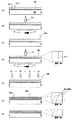
まず、実施の形態2にしたがって、基板500上に下地絶縁膜501a、501b、非晶質半導体層503までを形成する。但し、本実施の形態では、半導体層504の厚さは55〜140nm(好ましくは60〜120nm)とする。
【0066】
次に実施の形態4にしたがって、Niを含む溶液504を塗布し、Niを含む液体の層505を形成し、結晶化を行って非晶質半導体層503を結晶質半導体層506とする。この時点で、結晶質半導体層506の中にはNiが高濃度に残存している。その濃度分布は図3(D)に添付のグラフのようになる。
【0067】
次に、リンを含む液体507(代表的にはリン酸水溶液)をスピナーを用いて塗布し(図3(D))、半導体層の表面にリンを含む液体の薄い膜508を形成する。この状態の基板に対して、実施の形態2と同様にレーザー光を照射する(図3(E))。
【0068】
その結果、半導体層は溶融状態となり、リンが取り込まれるが。この際、半導体層の再結晶は基板側から始まるため、リンの濃度は半導体層の表面に近づくにつれ、高くなって行く。ここで、Niの固溶度はリンなど不純物の濃度が高くなるほど大きくなるため、Niの濃度も半導体層の表面に近づくにしたがって大きくなって行き、半導体層表面にリン、ニッケルのどちらの濃度も高い領域509bが形成される(図3(F))。
【0069】
この、リン、ニッケルが共に高い領域509bをエッチングにより、30〜60nm程度除去することで、ゲッタリングが完了する。この場合のリンを含む液体のリン濃度はゲッタリング工程により除去されない部分509aに所望の濃度のリンが取り込まれる程度に調節すれば良い。エッチングはCMP法に代えても良い。
【0070】
本発明を使用することにより、本発明のレーザードーピングの工程に、半導体の表層部を除去するエッチングやCMPの工程を付け加えるのみで、結晶化を助長する元素のゲッタリングまで行うことが可能となり、大幅な工程の短縮となる。
【0071】
なお、本実施の形態は、実施の形態2とも組み合わせて使用することが可能である。
【0072】
(実施の形態6)
本実施の形態では、レーザードーピング法を使用して、ドーピング深さを制御し短チャネル効果を抑制する浅いpn接合を形成する方法について説明する。
【0073】
レーザードーピング法では、レーザー光が照射され、半導体層が溶融することによりドーパントが取り込まれるため、ドーパントは溶融した部分にのみ添加される。また、レーザードーピング法でドーパントが添加された層は活性が高く、その後のアニールも必要としない場合が多いので、ドーピング工程後のアニールなどによる拡散の心配が無い。
【0074】
レーザードーピングによってドーパントを添加する際、半導体膜が溶融する深さに影響するのは、照射強度、照射時間及び波長である。同時間、同波長で照射するのであれば照射強度は高ければ深いところまで溶融するし、低ければ浅いところまでしか溶融しない。照射時間については、照射時間が長ければそれだけ多くのエネルギーが1箇所に与えられることになるため、溶融する深さが深くなる。波長については、半導体膜に対するレーザー光の吸収係数が波長により異なっているために溶融深さに影響する。
【0075】
波長が308nmのXeClエキシマレーザーをシリコンに照射した場合、300nm付近のシリコンの吸収係数が大きいため、レーザー光が直接シリコンに吸収されるのは約30nmの深さまでである。それより深い位置は、30nmにまで吸収されたレーザー光により発生した熱で徐々に溶融していく。
【0076】
一方、用いられることの多い、波長が532nmのNd:YAGレーザーの第2高調波を使用した場合、シリコンの該波長付近での吸収係数が小さく、半導体層の深い部分にまで、レーザー光が侵入する。そのため、この波長では深さ制御を行うことが難しいことから、YAGレーザーなど、波長が長いレーザーは非線型光学素子を用いて、第3高調波などに変換し、半導体層の吸収係数が大きい紫外領域の波長のレーザーに変換して使用すると良い。
【0077】
本実施の形態ではエキシマレーザーの基本波を使用し、300mj/cm2のエネルギー密度でレーザードーピングを行い、半導体層表面から40nm程度に浅くドーピングされた領域を形成することができる。本実施の形態には、Cr3+、Cr4+、Nd3+、Er3+、Ce3+、Co2+、Ti3+、Yb3+又はV3+がドーピングされたYAG、YVO4、YLF、YAlO3などの結晶を使った固体レーザーも使用することができ、これらのレーザーは基本波長を非線型光学素子を用いて紫外領域の高次高調波に変換することで、本実施の形態に使用することができるようになる。
【0078】
本実施の形態は、ソース領域やドレイン領域への不純物の添加に好適に用いることができ、特に、年々縮小されるデザインルールに対応して短くなったチャネル領域に起因して発生する短チャネル効果を、本法を使用することで浅い接合を形成することにより抑制することが可能となる。
また、本実施の形態は実施の形態1〜5と組み合わせて使用することができる。
【0079】
(実施の形態7)
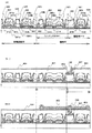
本発明を使用して、TFTを作製する方法について図4を使用して説明する。実施の形態2に示したように基板300上に下地絶縁膜301a、301b、結晶質半導体膜までを作製したら、結晶質半導体膜をエッチングにより所望の形状の結晶質半導体層302〜305とする。なお、半導体層を所望の形状にエッチングして非晶質半導体層としてから、前記結晶化処理を行っても構わない。また、結晶化のために使用したニッケルのゲッタリングを行っても良い。ゲッタリングは、実施の形態5で示した方法で行うと、チャネルドーピング工程にエッチング処理又はCMP処理を加えるだけで行うことができるので、工程の短縮につながる。もちろん他の公知の方法を使用してゲッタリングを行っても良い。
【0080】
他の方法でゲッタリングを行う場合は、例えば次のような方法がある。表面をオゾン水で処理し、1〜5nm程度のバリア膜を形成してから、該バリア層上にスパッタリング法にてゲッタリングサイトを形成する。ゲッタリングサイトはアルゴン元素を含む非晶質シリコン膜を膜厚150nm堆積することで形成する。成膜条件は、成膜圧力:0.3Pa、ガス(Ar)流量:50(sccm)、成膜パワー:3kW、基板温度:150℃とした。なお、上記条件での非晶質シリコン膜に含まれるアルゴン元素の原子濃度は、3×10²⁰/cm3〜6×1020/cm3、酸素の原子濃度は1×1019/cm3〜3×1019/cm3程度である。その後、ランプアニール装置を用いて650℃、3分の熱処理を行いゲッタリングする。ゲッタリング領域はエッチングなどで除去すれば良い。
【0081】
続いて、ゲート絶縁膜306を形成する。膜厚は115nm程度とし、減圧CVD法またはプラズマCVD法、スパッタ法などでシリコンを含む絶縁膜を形成すれば良い。本実施の形態では酸化シリコン膜を10nmの厚さで用いる。この場合、プラズマCVD法でTEOS(Tetraethyl Ortho Silicate)とO2とを混合し、反応圧力40Pa、基板温度300〜400℃の条件下で、高周波(13.56MHz)電力密度0.5〜0.8W/cm2で放電させて形成することができる。このようにして作製される酸化シリコン膜は、その後400〜500℃の加熱処理によりゲート絶縁膜として良好な特性を得ることができる。
【0082】
次いで、ゲート絶縁膜上に膜厚20〜100nmの第1の導電膜と第1の導電膜上に膜厚100〜400nmの第2の導電膜を形成する。本実施の形態では第1の導電膜としてTaNを30nm、第2の導電層としてWを370nmで形成した。TaN膜、W膜共スパッタ法で形成すればよく、TaN膜はTaのターゲットを用いて窒素雰囲気中で、W膜はWのターゲットを用いて成膜すれば良い。ゲート電極として使用するには抵抗が低いことが要求され、特にW膜の抵抗率は20μΩcm以下であることが望ましいため、Wのターゲットは高純度(99.9999%)のターゲットを用いることが望ましく、成膜時の不純物混入にも注意をはらわなければならない。こうして形成されたW膜の低効率は9〜20μΩcmとすることが可能である。
【0083】
なお、本実施の形態では第1の導電層をTaN、第2の導電層をWとしたが、これに限定されず、第1の導電層と第2の導電層は共にTa、W、Ti、Mo、Al、Cu、Cr、Ndから選ばれた元素、または前記元素を主成分とする合金材料若しくは化合物材料で形成してもよい。また、リン等の不純物元素をドーピングした多結晶珪素膜に代表される半導体膜を用いてもよい。また、AgPdCu合金を用いてもよい。さらに、その組み合わせも適宜選択すればよい。また、本実施の形態では、2層の積層構造としたが、1層としてもよいし、もしくは3層以上の積層構造としてもよい。
【0084】
次に、前記導電層をエッチングして電極及び配線を形成するため、フォトリソグラフィーにより露光工程を経てレジストからなるマスクを形成し、エッチングを行う。
【0085】
第1のエッチング処理では第1のエッチング条件と第2のエッチング条件でエッチングを行う。レジストによるマスクを用い、エッチングし、ゲート電極及び配線を形成する。エッチング条件は適宜選択すれば良い
【0086】
本法では、ICP(Inductively Coupled Plasma:誘導結合プラズマ)エッチング法を使用する。第1のエッチング条件として、エッチング用ガスにCF4、Cl2とO2を用い、それぞれのガス流量比を25/25/10(sccm)とし、1.0Paの圧力でコイル型電極に500WのRF(13.56MHz)電力を投入してプラズマを生成してエッチングを行う。基板側(試料ステージ)にも150WのRF(13.56MHz)電力を投入し、実質的に負の自己バイアス電圧を印加する。この第1のエッチング条件によりW膜をエッチングして第1の導電層の端部をテーパー形状とする。第1のエッチング条件でのW膜に対するエッチング速度は200.39nm/min、TaNに対するエッチング速度は80.32nm/min、でありTaNに対するWの選択比は約2.5である。また、この第1のエッチング条件によって、W膜のテーパー角度は約26°となる。
【0087】
続いて、第2のエッチング条件に移ってエッチングを行う。レジストからなるマスクを除去せず、のこしたまま、エッチング用ガスにCF4とCl2を用い、それぞれのガス流量比を30/30(sccm)、圧力1.0Paでコイル型の電極に500WのRF(13.56MHz)電力を投入してプラズマを生成して約15秒程度のエッチングを行う。基板側(試料ステージ)にも20WのRF(13.56MHz)電力を投入し、実質的に負の自己バイアス電圧を印加する。CF4とCl2を混合した第2のエッチング条件ではW膜及びTaN膜とも同程度にエッチングされる。この第1のエッチング処理において、電極に覆われていないゲート絶縁膜は20nm〜50nm程度エッチングされる。
【0088】
上記の第1のエッチング処理においては、基板側に印加されたバイアス電圧の効果により第1の導電層及び第2の導電層の端部はテーパー状となる。このように第1のエッチング処理においては、第1の導電層と第2の導電層からなる第1形状の導電層が形成される。
【0089】
次いで、レジストからなるマスクを除去せずに第2のエッチング処理を行う。第2のエッチング処理では、エッチング用のガスにSF6とCl2とO2を用い、それぞれのガス流量比を24/12/24(sccm)とし、1.3Paの圧力でコイル側の電力に700WのRF(13.56MHz)電力を投入してプラズマを発生して25秒程度エッチングを行う。基板側(試料ステージ)にも10WのRF(13.56MHz)電力を投入し、実質的に負の自己バイアス電圧を印加する。このエッチング条件ではW膜が選択的にエッチングされ、第2形状の導電層307a〜310a、307b〜310bが形成される。
【0090】
そして、レジストからなるマスクを除去せず、第1のドーピング処理を行う。これにより、結晶質半導体層302〜305にN型を付与する不純物が低濃度に添加される。第1のドーピング処理はイオンドープ法又はイオン注入法で行えば良い。イオンドープ法の条件はドーズ量が1×10¹³〜5×10¹⁴atoms/cm2、加速電圧が40〜80kVで行えばよい。本実施の形態では加速電圧を50kVとして行った。N型を付与する不純物元素としては15族に属する元素を用いることができ、代表的にはリン(P)または砒素(As)が用いられる。本実施の形態ではリン(P)を使用した。その際、第1の導電層307a〜310aをマスクとして、自己整合的に低濃度の不純物が添加されている第1の不純物領域(N−−領域)を形成した。
【0091】
続き、レジストからなるマスクを除去する。そして新たにレジストからなるマスクを、半導体層304の低濃度不純物領域を形成する場所と、及びPチャネルTFTを作製する半導体層303、305を覆って形成し、第1のドーピング処理よりも高い加速電圧で、第2のドーピング処理を行う。第2のドーピング処理もN型を付与する不純物を添加する。イオンドープ法の条件はドーズ量を1×10¹³〜3×10¹⁵atoms/cm2、加速電圧を60〜120kVとすれば良い。本実施の形態ではドーズ量を3.0×1015atoms/cm2とし、加速電圧を65kVとして行った。第2のドーピング処理は第2の導電層を不純物元素に対するマスクとして用い、第1の導電層の下方に位置する半導体層にも不純物元素が添加されるようにドーピングを行う。
【0092】
第2のドーピングを行うと、結晶質半導体層302〜305の第1の導電層307a〜310aと重なっている部分のうち、第2の導電層307b〜310bに重なっていない部分、もしくはマスクに覆われていない部分に、第2の不純物領域(N−領域、Lov領域)311が形成される。第2の不純物領域311には1×10¹⁸〜5×10¹⁹atoms/cm3の濃度範囲でN型を付与する不純物が添加される。また、結晶質半導体層302〜305のうち、第1形状の導電層307a〜310aにもマスクにも覆われておらず、露出している部分(第3の不純物領域:N+領域)312、313には、1×1019〜5×1021atom/cm3の範囲で高濃度にN型を付与する不純物が添加される。また、半導体層304にはN+領域が存在するが、一部マスクのみに覆われている部分314がある。この部分のN型を付与する不純物の濃度は、第1のドーピング処理で添加された不純物濃度のままである。
【0093】
なお、本実施の形態では2回のドーピング処理により各不純物領域を形成したが、これに限定されることは無く、適宜条件を設定して、一回もしくは複数回のドーピングによって所望の不純物濃度を有する不純物領域を形成すれば良い。
【0094】
次いで、レジストからなるマスクを除去した後、Nチャネル型TFTを形成する半導体層302、304上に、新たにレジストからなるマスクを形成し、第3のドーピング処理を行う。第3のドーピング処理により、Pチャネル型TFTとなる半導体層に前記第1の導電型及び前記第2の導電型とは逆の導電型を付与する不純物元素が添加された、第4の不純物領域(P+領域)315、316及び第5の不純物領域(P−領域)317、318が形成される。
【0095】
第3のドーピング処理では、レジストからなるマスクに覆われておらず、更に第1の導電層とも重なっていない部分315、316に、第4の不純物領域(P+領域)が形成され、レジストからなるマスクに覆われておらず、且つ第1の導電層と重なっており、第2の導電層と重なっていない部分317、318に第5の不純物領域(P−領域)が形成される。P型を付与する不純物元素としては、ホウ素(B)、アルミニウム(Al)、ガリウム(Ga)など周期律表第13族の元素が知られている。
【0096】
本実施の形態では、第4の不純物領域及び第5の不純物領域を形成するP型の不純物元素としてはホウ素(B)を選択し、ジボラン(B2H6)を用いたイオンドープ法で形成した。イオンドープ法の条件としては、ドーズ量を1×10¹⁶atoms/cm2とし、加速電圧を80kVとした。
【0097】
ここで、第1及び第2のドーピング処理によって、第4の不純物領域(P+領域)315、316及び第5の不純物領域(P−領域)317、318にはそれぞれ異なる濃度でリンが添加されている。しかし、第4の不純物領域(P+領域)315、316及び第5の不純物領域(P−領域317、318のいずれの領域においても、第3のドーピング処理によって、P型を付与する不純物元素の濃度が1×10¹⁹〜5×10²¹atoms/cm2となるようにドーピング処理される。そのため、第4の不純物領域(P+領域)315、316及び第5の不純物領域(P−領域)317、318は、Pチャネル型TFTのソース領域及びドレイン領域として問題無く機能する。
【0098】
なお、本実施の形態では、第3のドーピング一回で、第4の不純物領域(P+領域)315、316及び第5の不純物領域(P−領域)317、318を形成したが、これに限定はされない。ドーピング処理の条件によって適宜複数回のドーピング処理により第4の不純物領域(P+領域)315、316及び第5の不純物領域(P−領域)317、318を形成してもよい。
【0099】
次いで、レジストからなるマスクを除去して第1のパッシベーション膜319を形成する。この第1のパッシベーション膜としてはシリコンを含む絶縁膜を100〜200nmの厚さに形成する。成膜法としてはプラズマCVD法や、スパッタ法を用いればよい。本実施の形態では、プラズマCVD法により膜厚100nmの酸化窒化珪素膜を形成した。酸化窒化シリコン膜を用いる場合には、プラズマCVD法でSiH4、N2O、NH3から作製される酸化窒化シリコン膜、またはSiH4、N2Oから作製される酸化窒化シリコン膜を形成すれば良い。この場合の作製条件は反応圧力20〜200Pa、基板温度300〜400℃とし、高周波(60MHz)電力密度0.1〜1.0W/cm2である。また、第1のパッシベーション膜319としてSiH4、N2O、H2から作製される酸化窒化水素化シリコン膜を適用しても良い。もちろん、第1のパッシベーション膜319は、本実施の形態のような酸化窒化シリコン膜の単層構造に限定されるものではなく、他のシリコンを含む絶縁膜を単層構造、もしくは積層構造として用いても良い。
【0100】
その後、加熱処理(熱処理)を行って、半導体層の結晶性の回復、半導体層に添加された不純物元素の活性化を行う。熱アニール法としては、酸素濃度が1ppm以下、好ましくは0.1ppm以下の窒素雰囲気中で400〜700℃で行えば良く、本実施の形態では410℃、1時間の熱処理で活性化処理を行った。なお、熱アニール法の他に、レーザーアニール法、又はラピッドサーマルアニール法(RTA法)を適用することができる。
【0101】
また、第1のパッシベーション膜319を形成した後で熱処理を行うことで、活性化処理と同時に半導体層の水素化も行うことができる。水素化は、第1のパッシベーション膜319に含まれる水素によって、半導体層のダングリングボンドを終端するものである。
【0102】
また、第1のパッシベーション膜319を形成する前に加熱処理を行ってもよい。但し、第1の導電層及び第2の導電層を構成する材料が熱に弱い場合には、本実施の形態のように配線などを保護するため、第1のパッシベーション膜319を形成した後で熱処理を行うことが望ましい。さらに、この場合、第1のパッシベーション膜319がないため、当然パッシベーション膜に含まれる水素を利用しての水素化は行うことができない。
【0103】
この場合は、プラズマにより励起された水素を用いる手段(プラズマ水素化)を用いての水素化や、3〜100%の水素を含む雰囲気中において、300〜450℃で1〜12時間の加熱処理による水素化を用いれば良い。
【0104】
次いで、第1のパッシベーション膜319上に、第1の層間絶縁膜320を形成する。第1の層間絶縁膜320としては、無機絶縁膜や有機絶縁膜を用いることができる。無機絶縁膜としては、CVD法により形成された酸化シリコン膜や、SOG(Spin On Glass)法により塗布された酸化シリコン膜などを用いることができ、有機絶縁膜としてはポリイミド、ポリアミド、BCB(ベンゾシクロブテン)、アクリルまたはポジ型感光性有機樹脂、ネガ型感光性有機樹脂等の膜を用いることができる。また、アクリル膜と酸化窒化シリコン膜の積層構造を用いても良い。
【0105】
本実施の形態では、膜厚1.6μmの非感光性アクリル膜を形成した。第1の層間絶縁膜320によって、TFTによる凹凸を緩和し、平坦化することができる。とくに、第1の層間絶縁膜320は平坦化の意味合いが強いので、平坦化されやすい材質の絶縁膜を用いることが好ましい。
【0106】
その後、第1の層間絶縁膜320上に窒化酸化シリコン膜等からなる第2のパッシベーション膜321を形成する。膜厚は10〜200nm程度で形成すれば良く、第2のパッシベーション膜によって第1の層間絶縁膜320へ水分が出入りすることを抑制することができる。また、第2のパッシベーション膜には、窒化シリコン膜、窒化アルミニウム膜、酸化窒化アルミニウム膜、ダイヤモンドライクカーボン(DLC)膜やカーボンナイトライド(CN)膜も同様に使用できる。
【0107】
またRFスパッタ法を用いて成膜された膜は緻密性が高く、バリア性に優れている。RFスパッタの条件は、例えば酸化窒化珪素膜を成膜する場合、Siターゲットで、N2、Ar、N2Oをガスの流量比が31:5:4となるように流し、圧力0.4Pa、電力3000Wとして成膜する。また、例えば窒化珪素膜を成膜する場合、Siターゲットで、チャンバー内のN2、Arをガスの流量比が20:20となるように流し、圧力0.8Pa、電力3000W、成膜温度を215℃として成膜する。本実施の形態では、第2のパッシベーション膜321はRFスパッタ法を用いて、酸化窒化シリコン膜を70nmの膜厚で形成した。
【0108】
次いで、エッチングにより第2のパッシベーション膜321、第1の層間絶縁膜320及び第1のパッシベーション膜319をエッチングし、第3の不純物領域312、313及び第4の不純物領域315、316に達するコンタクトホールを形成する。
【0109】
続いて、各不純物領域とそれぞれ電気的に接続する配線322〜328及び電極329を形成する。なお、これらの配線は、膜厚50nmのTi膜と膜厚500nmの合金膜(AlとTi)との積層膜をパターニングして形成する。もちろん、に2層構造に限らず、単層構造でも良いし、3層以上の積層構造にしても良い。また、配線材料としては、AlとTiに限らない。例えばTaN膜上にAl膜やCu膜を形成し、更にTi膜を形成した積層膜をパターニングして配線を形成しても良い。
【0110】
本発明はこのようにして、図4の形態を得ることができ、液体によりドーパントを塗布した後レーザー照射によりドーパントを半導体層に添加することで、容易に大面積基板にも精密な濃度制御を行ったチャネルドーピングをすることができる。さらに、本発明をもちいることによって、精密なしきい値電圧制御を行ったTFTを作製することができる。
【0111】
なお、本実施の形態は実施の形態1〜6と適宜組み合わせ、もしくは差し替えて使用することができる。
【0112】
(実施の形態8)
本実施の形態では、本発明を使用して作製したTFTを用いて表示装置を作製する例について図4及び図5を用いて説明する。
【0113】
図4に示した本発明のTFTを作製後、TFTの配線327と一部重なるように、透明導電膜からなる第1の電極400を形成する。透明導電膜としては仕事関数の大きい材質を用いて作製することが望ましく、酸化インジウムと酸化スズの化合物(ITO)、酸化インジウムと酸化亜鉛の化合物、酸化亜鉛、酸化スズ、酸化インジウム、窒化チタンなどを用いることができる。また、前記透明導電膜にガリウムを添加して作製した膜やITO膜をスパッタ法で作製する際、ターゲットにSiO2を混ぜて作製した膜を用いても良い。この第1の電極400が発光素子の陽極となる。本実施の形態では第1の電極400にはITOを使用した。ITOは0.1μmの厚みにスパッタ法により形成した。
【0114】
また、この透明導電膜を形成する方法は、本実施の形態で示したようにTFTの配線327を形成した後に形成する方法の他、図5(i)に示したように配線327を形成する前に形成する方法(図5(i)B)、配線327形成後、絶縁物を形成してからコンタクトホールを開口して形成する方法(図5(i)C)などの方法で形成してもよい。図5(i)Aは本法の形態である。
【0115】
次いで、電極の端面を覆うように絶縁物401を形成する。絶縁物401は無機または有機の材料で形成することができるが、感光性の有機物を使用して形成すると、開口部の形状が発光層を蒸着する際に段切れなどが起こりにくいものとなり好適である。例えば、絶縁物401の材料としてネガ型の感光性アクリルを用いた場合、図5(ii)Aのように、絶縁物401の上端部に第1の曲率半径を有する曲面を有し、前記絶縁物の下端部に第2の曲率半径を有する曲面を有するように形成することができる。前記第1の曲率半径及び前記第2の曲率半径は、0.2μm〜3μm、また前記開口部の壁面のITOに対する角度は35°以上とすることが好ましい。また、感光性はネガ型に限らずポジ型を用いることができる。その際、ポジ型を用いた場合の開口部の形状は図5(ii)Bのように絶縁物の上端部は曲率半径を有する曲面となる。感光性の有機物を用いず、絶縁物401の開口部をドライエッチングで作製した場合は図5(ii)Cのような形状となる。
【0116】
その後、PVA(ポリビニルアルコール)系の多孔質体を用いて拭い、ゴミ等の除去を行う。なお本実施の形態では、PVAの多孔質体を用いた拭浄により、ITOや絶縁膜をエッチングしたときに発生する微粉(ゴミ)の除去を行った。
【0117】
次いで発光層の蒸着前処理に、全体にPEDOTを塗布し、ベークを行ってもよい。このとき、PEDOTはITOとの濡れ性が良くないため、一旦PEDOTを塗布後、水洗し、再度PEDOTを塗布することが好ましい。その後、常圧で加熱を行って水分を飛ばしてから、減圧雰囲気で加熱を行う。なお、本実施の形態では、PEDOTを塗布後、170℃の減圧雰囲気で4時間加熱し、その後30分かけて自然冷却を行う。
【0118】
そして、蒸着装置を用いて、蒸着源を移動させながら蒸着を行う。例えば、真空度が5×10⁻³Torr(0.665Pa)以下、好ましくは10−4〜10−6Torrまで真空排気された成膜室で蒸着を行う。蒸着の際、抵抗加熱により、予め有機化合物は気化されており、蒸着時にシャッターが開くことにより基板の方向へ飛散する。気化された有機化合物は、上方に飛散し、メタルマスクに設けられた開口部を通って基板に蒸着され、発光層402(正孔輸送層、正孔注入層、電子輸送層、電子注入層を含む)が形成される。
【0119】
ここでは蒸着法により発光層402を形成した例を示したが、特に限定されず、塗布法(スピンコート法、インクジェット法など)により高分子からなる発光層を形成してもよい。また、本実施の形態では、有機化合物層として低分子材料からなる層を積層した例を示したが、高分子材料からなる層と、低分子材料からなる層とを積層してもよい。また、RGBの発光層を形成してフルカラー表示を行っても、単色の発光層を形成し、色変換層やカラーフィルターを用いて、フルカラー表示を行ってもよい。また、無機の材料を用いても良い。
【0120】
発光素子の発光機構は、一対の電極間に有機化合物層を挟んで電圧を印加することにより、陰極から注入された電子および陽極から注入された正孔が有機化合物層中の発光中心で再結合して分子励起子を形成し、その分子励起子が基底状態に戻る際にエネルギーを放出して発光するといわれている。励起状態には一重項励起と三重項励起が知られ、発光はどちらの励起状態を経ても可能であると考えられている。
【0121】
発光層は通常、積層構造となっており、この積層構造は「正孔輸送層/電界発光層/電子輸送層」という構成が代表的である。この構造は非常に発光効率が高いため、現在研究開発が進められている発光装置はほとんどこの構造が採用されている。また、他にも陽極上に正孔注入層/正孔輸送層/電界発光層/電子輸送層、または正孔注入層/正孔輸送層/電界発光層/電子輸送層/電子注入層の順に積層する構造も良い。電界発光層に対して蛍光性色素等をドーピングしても良い。
【0122】
なお、本明細書において、陰極と陽極との間に設けられる全ての層を総称して発光層という。したがって、上述した正孔注入層、正孔輸送層、電界発光層、電子輸送層及び電子注入層は、全て発光層に含まれるものとする。これらは、低分子系有機化合物材料、中分子系有機化合物材料、又は高分子系有機化合物材料のいずれか、或いは、両者を適宣組み合わせて形成することが可能である。また、電子輸送性材料と正孔輸送性材料を適宜混合させた混合層、又はそれぞれの接合界面に混合領域を形成した混合接合を形成しても良い。又、有機系の材料のほかに無機系の発光材料を使用しても良い。
【0123】
次いで、上記発光層402上に、第2の電極403を陰極として形成する。第2の電極403は、仕事関数の小さい金属(Li、Mg、Cs)を含む薄膜を用いて形成すればよい。また更に、Li、Mg、Cs等を含む薄膜上に積層した透明導電膜(ITO(酸化インジウム酸化スズ合金)、酸化インジウム酸化亜鉛合金(In2O3―ZnO)、酸化亜鉛(ZnO)等)との積層膜で形成すると好ましい。膜厚は陰極として作用するように適宜設定すればよいが、0.01〜1μm程度の厚さに電子ビーム蒸着法で形成すればよい。
【0124】
ここで、電子ビーム蒸着法を用いると、加速電圧が高すぎた場合放射線を発生し、TFTにダメージを与えてしまう。しかし、加速電圧が低すぎても成膜速度が下がり、生産性が低下するため対策として、第2の電極403を陰極として作用しうる膜厚より過剰には成膜しないようにする。陰極が薄ければ成膜速度が遅くても生産性にさほどの影響は現れない。この場合陰極の膜厚が薄いことで高抵抗化してしまう問題も発生するが、陰極上に低抵抗金属であるAlなどを抵抗加熱蒸着やスパッタ法などで形成し、積層構造とすることで解決できる。
【0125】
次に、絶縁物401及び第2の電極403上に、第3のパッシベーション膜404を成膜した。第2のパッシベーション膜321と第3のパッシベーション膜404は、共に水分や酸素などの発光素子の劣化を促進させる原因となる物質を、他の絶縁膜と比較して透過させにくい膜を用いる。代表的には、例えばDLC膜、窒化炭素膜、RFスパッタ法で形成された窒化珪素膜等を用いるのが望ましい。またその膜厚は、10〜200nm程度とするのが望ましい。
【0126】
こうして図4(B−1)に示すような発光素子を得ることができる。図示しないが、その上にシーリング材としてプラスチックフィルムを設け、間の空間に不活性気体を充填する。そして異方性導電膜を用いてFPC(フレキシブルプリントサーキット)により外部端子と接続することで発光表示装置(表示モジュール)が完成する。
【0127】
本実施の形態は基板側(底面)から光を取り出す例を示したが、上面から光を取り出すようにするには、積層構造を図4(B−2)に示すようにする。その際は、第2の電極は透光性を有する材料で形成すれば良い。
【0128】
本発明を用い、しきい値電圧が精密に制御されたTFTを使用して表示装置を作製することにより、発光素子の輝度のバラツキが少なくなり、より高品質な画像を提供することができる表示装置を作製することができる。
【0129】
なお、本実施の形態は実施の形態1〜7と適宜組み合わせ、もしくは差し替えて使用することができる。
【0130】
【発明の効果】
本発明によって、しきい値制御のために濃度制御が非常に重要なチャネルドーピングを、精度良く、大面積に効率良く施すことができる。また、レーザーとそのエネルギーを適切に選ぶことによって、半導体層の表面極浅い部分のみに選択的にドーピングを行うことが可能となる。さらに、ドーピングすることによって結晶構造を破壊しないため、イオン注入法や、プラズマドーピング法を行った後に必要である活性化の作業を必要とせず、工程の短縮及び歩留まりの改善が期待できる。
【0131】
また、本発明によって、大幅な工程の追加をせずとも、半導体の特性に悪影響を及ぼす、半導体中に残存した過剰の結晶化を助長する元素を除去することが可能となり、スループットの向上、歩留まりの改善が期待できる。
【図面の簡単な説明】
【図1】本発明の実施の一例を示す図。
【図2】本発明の実施の一例を示す図。
【図3】本発明の実施の一例を示す図。
【図4】本発明の実施の一例を示す図。
【図5】本発明の実施の一例を示す図。[0001]
TECHNICAL FIELD OF THE INVENTION
The present invention relates to a method for doping a semiconductor with impurities. In particular, the present invention relates to channel doping, which requires precise control of the amount of an impurity to be doped, and to a laser doping method for adding an impurity to a semiconductor by irradiating laser light.
[0002]
[Prior art]
In order to utilize the electrical properties of a semiconductor and to control the electrical properties when a semiconductor element is manufactured, a technique called doping for adding a small amount of impurities to a semiconductor is currently widely used. The method of doping a semiconductor can be roughly classified into a method of adding an impurity in a process of forming a semiconductor from a raw material and a method of adding an impurity after forming a semiconductor. As a method for adding an impurity, an ion implantation method, a plasma doping method, a laser doping method, or the like is typically given.
[0003]
In the ion implantation method, an ion beam is extracted by adding a gas containing a dopant to a plasma chamber, and the ion beam is accelerated at an energy of several keV to several hundred keV by applying the ion beam to a mass analyzer. This is a method of causing collision and physically adding a dopant. The plasma doping method is a method in which doping is performed by exposing a semiconductor to plasma containing a dopant gas diluted to a desired concentration or exposing the semiconductor to ions extracted from the plasma. Since the plasma doping method does not perform mass spectrometry, various forms of ions generated in the plasma are doped.
[0004]
As one form of the doping method, a laser doping method is also used. The laser doping method is a method in which a semiconductor is placed in a gas containing a dopant, and the surface is irradiated with a laser beam to be melt-added and activated. Although the laser doping method can be used for a wide range of doping and high activation, studies have been made to further increase the efficiency, such as heating a sample or irradiating a laser while applying electromagnetic energy (for example, And Patent Document 1).
[0005]
On the other hand, in the semiconductor world, speeding up and miniaturization are progressing at a rapid pace. Accordingly, there is a strong demand for improved reliability of semiconductors and circuits. A threshold voltage is often used as one parameter for evaluating a semiconductor element. However, if the threshold voltage is too high or too low, it lacks reliability, and it is most important that a desired threshold voltage can be obtained. is there.
[0006]
As a means for controlling the threshold voltage, a technique called channel doping is used. As the name implies, channel doping is a technique in which a trace amount of impurities is added to a portion to be a channel formation region so that a desired threshold voltage can be obtained. Since the purpose of channel doping is to precisely control the change in threshold voltage, it is necessary to precisely control the amount of addition.
[0007]
The amount of injected ions in the ion implantation method or the plasma doping method is controlled using a Faraday cup ammeter that measures flowing ions as current. An ion implantation method capable of doping only necessary ions can be suitably used for channel doping requiring precise concentration control.
[0008]
Further, in order to realize high speed and miniaturization, it is necessary to shorten the gate length. However, when the gate length is shortened, a current leaks in a deep portion of a channel formation region, that is, a so-called short channel effect occurs, which is a problem. To prevent this, it is effective to add an impurity only to a very shallow portion of the source region and the drain region (form a shallow junction).
[0009]
Meanwhile, as a technique for forming a crystalline semiconductor layer on a substrate having low heat resistance, such as a glass substrate, there is a technique using an element such as Ni that promotes crystallization. After forming amorphous silicon on a glass substrate and applying a solution containing Ni by a spinner or forming a thin film of Ni by sputtering or the like, crystallization is performed, so that crystallization is performed in a short time at low temperature. Technology. This technology is an indispensable technology to reduce the price of a product by using an inexpensive glass substrate.
[0010]
[Patent Document 1]
JP-A-5-326430
[0011]
[Problems to be solved by the invention]
As a problem of doping, there is a current situation in which the circuit size is increasing year by year and the size of the display is increasing, so that the size of the substrate flowing in the manufacturing process is increasing and the area requiring doping is also increasing.
[0012]
In the ion implantation method, it is necessary to narrow the beam in order to accurately separate the mass of the ion beam. For this reason, doping cannot be performed over a wide area at once, and the processing takes an enormous amount of time. Therefore, there is a serious problem that a wide range of doping processing cannot be handled.
[0013]
In addition, in order to form a shallow junction in the ion implantation method, ions must be implanted with low energy, but an ion beam of low energy diverges, and it is difficult to obtain a sufficient amount of current. There are also problems. Further, the dopant diffuses due to thermal annealing for recovering damage due to ion implantation, and it is very difficult to add an impurity only to an extremely shallow region.
[0014]
In addition, the plasma doping method is more advantageous than the ion implantation method in terms of processing time, but since no mass separation is performed, the ion current measured by the Faraday cup ammeter is equal to the ion of the gas diluted with the dopant gas. This is the total ion current including the dopant ions. Therefore, even if the total ion doping amount is accurately controlled, if the ratio of the gas diluting the dopant gas to the dopant gas, that is, the ion ratio ratio changes during the operation of the apparatus, the amount of the implanted dopant also changes. I will. Therefore, there is a problem in applying to channel doping that requires precise concentration control.
[0015]
On the other hand, in the laser doping method, in which a method of irradiating a laser beam in a dopant gas atmosphere, which is widely used, it is difficult to control the amount of a dopant to be implanted, and a special device is required to uniformly distribute the dopant. turn into.
[0016]
Another problem is that elements that promote crystallization have a very advantageous effect on crystallization. However, if a large amount of these elements remain in the semiconductor layer after crystallization, TFTs may be formed using the semiconductor layer. In particular, when a channel region of a TFT is manufactured, the characteristics of the TFT are adversely affected. Therefore, when crystallization is performed using these elements that promote crystallization, a means for reducing the concentration of the elements called gettering is usually taken.
[0017]
Gettering is performed by moving from a region in which it is inconvenient if a large amount of an element promoting crystallization remains to another region (called a getterin region).
[0018]
Regarding the removal of the residual Ni element, the present applicant discloses a method by a gettering treatment (Japanese Patent Laid-Open No. Hei 10-214786). However, a mask forming step for selectively adding the Ni element and a gettering method are disclosed. A mask formation step for selectively adding elements is required, and heat treatment must be performed twice in the crystallization step and the gettering step. Had worsened.
[0019]
In view of these problems, it is an object of the present invention to provide a simple doping method that can easily perform concentration control, can practically perform doping over a large area, and does not require a special device. And
[0020]
Another object of the present invention is to provide a doping method capable of easily controlling the concentration in the depth direction, which can cope with a shallow junction or the like.
[0021]
It is another object to provide a gettering method that does not deteriorate productivity and cost.
[0022]
[Means for Solving the Problems]
Accordingly, in the present invention, a liquid containing a dopant (one conductivity type impurity for the purpose of controlling valence electrons) is applied to the surface of a semiconductor to be doped, and then the surface of the semiconductor is irradiated with a laser beam, whereby the dopant is applied. A laser doping method for adding GaN to the semiconductor is proposed.
[0023]
In this method, the concentration of the dopant to be added to the semiconductor can be easily controlled by adjusting the concentration of the dopant in the liquid containing the dopant in order to supply the dopant in the liquid. Therefore, it is possible to appropriately control the dopant concentration required for controlling the threshold voltage.
[0024]
In the laser doping treatment, a portion irradiated with the laser is melted, and the dopant is taken in. Therefore, by adjusting the energy given by the laser light, the depth of the semiconductor to be melted can be adjusted, so that the depth to which the dopant is added can be easily adjusted. Therefore, it is easy to form a shallow junction.
[0025]
Further, according to the present invention, a liquid containing a dopant is applied to an amorphous semiconductor layer formed over a substrate having an insulating surface, and the amorphous semiconductor layer is crystallized by irradiating a laser beam, At the same time as forming a semiconductor layer, a dopant is added to the crystalline semiconductor layer.
[0026]
With this configuration, the crystallization by the laser beam and the addition of the dopant can be performed at the same time, so that the process can be shortened and the throughput can be expected to be improved.
[0027]
The present invention also provides a method for applying a liquid containing a dopant and an element which promotes crystallization to an amorphous semiconductor layer formed over a substrate having an insulating surface, and irradiating the liquid with a laser beam. Is crystallized into a crystalline semiconductor layer, and at the same time, a dopant is added to the crystalline semiconductor layer.
[0028]
With this structure, an element that promotes crystallization can be added simultaneously with the dopant, and a crystalline semiconductor layer with good crystallinity can be obtained.In addition, the dopant can be added simultaneously with the crystallization, Shortening of the process and improvement of the throughput can be expected.
[0029]
Further, the present invention applies a liquid containing an element that promotes crystallization to an amorphous semiconductor layer formed over a substrate having an insulating surface, and crystallizes the amorphous semiconductor layer by heating the amorphous semiconductor layer. A liquid containing a dopant is applied onto the crystalline semiconductor layer, and the crystalline semiconductor layer is irradiated with laser light to add the dopant to the crystalline semiconductor layer.
[0030]
With this configuration, a dopant can be added to the semiconductor simultaneously with laser annealing after thermal crystallization using an element that promotes crystallization, leading to a reduction in the number of steps.
[0031]
In the present invention, in a semiconductor layer crystallized using an element which promotes crystallization, an element which promotes crystallization remains at a high concentration. When a liquid containing a dopant is applied to the semiconductor layer and laser light irradiation is performed, the semiconductor layer is melted and the dopant is taken in.However, since heat given by the laser light is dissipated from the substrate side, solidification does not occur. It starts from the substrate side. Then, the concentration of the dopant segregates so as to be farther from the substrate, that is, to be higher as approaching the surface of the semiconductor layer. Since the element that promotes crystallization tends to move to the side with a higher impurity concentration, the concentration of the element that promotes crystallization is similarly segregated to be higher toward the surface. A feature is that gettering is performed by removing a portion where both the element concentration and the dopant concentration that promote crystallization are high by etching or chemical mechanical polishing (CMP).
[0032]
With this configuration, gettering can be completed and a TFT having excellent characteristics can be manufactured by merely adding an etching or CMP step to the doping step without using a gettering method that greatly increases the number of steps. A crystalline semiconductor layer can be manufactured.
[0033]
In the present invention having the above configuration, the concentration of the added dopant can be controlled more accurately without the need for a special device, and the control of the depth at which the dopant is added is facilitated. In addition, there is an effect that the throughput is improved by shortening the process.
[0034]
Embodiment
(Embodiment 1)
In this embodiment, a method for doping a semiconductor by applying a liquid containing a dopant and applying laser light is described.
[0035]
A liquid containing a dopant is applied to the surface of the semiconductor with a spinner to form a thin film of the liquid containing the dopant. As the dopant, an element imparting N-type or P-type is used. Typically, phosphorus, arsenic, and antimony are used as N-type, and boron, aluminum, and gallium are used as P-type. The concentration is adjusted by adjusting the dopant concentration in the liquid so that a desired concentration is finally added to the semiconductor film.
[0036]
As a liquid containing an element imparting a P-type or an N-type, an aqueous solution of boric acid or phosphoric acid is typically given. When these aqueous solutions are applied to the surface of a semiconductor, the wettability between the semiconductor surface and water is not so good, and in order to improve the wettability, an ultrathin oxidation is performed by applying ozone water to the surface of the semiconductor film in advance. It is preferable to form a film. The element imparting the P-type or the N-type is not limited thereto, and may be appropriately dissolved in a solvent and applied, provided that the element does not contain an element that has a significant effect on the characteristics of the semiconductor. Can be used. Further, the solvent is not limited to water, and an organic solvent or the like can also be used in accordance with the element imparting P-type or N-type. For example, benzene, toluene, xylene, carbon tetrachloride, chloroform, ether, ethanol, and the like can be used as the organic solvent. In this case, an oxide film need not be formed on the surface of the semiconductor film. Further, the liquid to be applied is not limited to a solution, but may be a uniform dispersion, a colloid solution, or the like.
[0037]
After a liquid containing a dopant is applied, laser light is irradiated to perform doping. As a laser beam, a pulse oscillation type or continuous emission type gas laser, solid laser, or metal laser can be used. In the case of using these lasers, it is preferable to use a method in which laser light emitted from a laser oscillator is linearly condensed by an optical system and irradiated on a semiconductor film.
[0038]
By this laser irradiation, all or part of the semiconductor is melted, and the dopant is incorporated into the semiconductor layer by incorporating the dopant.
[0039]
As described above, by performing laser doping, a highly reliable TFT which can add a desired concentration of impurities to a semiconductor with high accuracy even on a large-area substrate can be obtained with high throughput.
[0040]
(Embodiment 2)
In this embodiment, a method for simultaneously performing crystallization and laser doping will be described with reference to FIGS.
[0041]
First,
[0042]
The
[0043]
Next, the
[0044]
Subsequently, a liquid 103 containing a dopant was applied by a spinner (FIG. 1B) to form a
[0045]
The boron concentration only needs to be such that boron can be finally added to the semiconductor film to obtain a desired threshold voltage. Fifteen ~ 1 × 10 18 atoms / cm 3 (Typically 5 × 10 16 ~ 5 × 10 17 atoms / cm 3 ) Adjust the concentration so that the concentration of the position is added.
[0046]
After the formation of the boric acid
[0047]
Excimer laser, Ar laser, Kr laser as gas laser, YAG laser, YVO as solid laser 4 Laser, YLF laser, YAlO 3 Examples of the laser, glass laser, ruby laser, alexandrite laser, Ti: sapphire laser, and metal laser include a helium cadmium laser, a copper vapor laser, and a gold vapor laser. The solid state laser is Cr 3+ , Cr 4+ , Nd 3+ , Er 3+ , Ce 3+ , Co 2+ , Ti 3+ , Yb 3+ Or V 3+ Doped YAG, YVO 4 , YLF, YAlO 3 A laser using a crystal such as the above can be used. The fundamental wave of the laser depends on the material to be doped, and a laser beam having a fundamental wave of about 1 μm can be obtained. Harmonics with respect to the fundamental wave can be obtained by using a nonlinear optical element.
[0048]
The conditions for laser irradiation are appropriately selected by the practitioner. When an excimer laser is used, the pulse oscillation frequency is set to 300 Hz, and the laser energy density is set to 100 to 400 mJ / cm. 2 (Typically 200 to 300 mJ / cm 2 ). When a YAG laser is used, its higher order harmonics are used, the pulse oscillation frequency is set to 30 to 300 kHz, and the laser energy density is set to 300 to 600 mJ / cm. 2 (Typically 350-500 mJ / cm 2 )) Then, a laser beam condensed linearly with a width of 100 to 1000 μm, for example, 400 μm, is irradiated over the entire surface of the substrate, and the superposition rate (overlap rate) of the linear laser light at this time is set to 50 to 90%.
[0049]
By the irradiation of the laser light, all or part of the
[0050]
In this way, by applying a boric acid aqueous solution and then irradiating with laser light under appropriate conditions, crystallization can be performed simultaneously with channel doping, and a desired concentration of impurity can be accurately added to a semiconductor. it can. In addition, since channel doping can be performed simultaneously with the crystallization step, a part of the channel doping step can be shortened, and improvement in efficiency can be expected. Further, by manufacturing a TFT using the semiconductor layer as a channel formation region, threshold voltage control becomes easy, and a highly reliable TFT can be obtained with higher throughput even on a large-area substrate.
[0051]
(Embodiment 3)
Another embodiment of the present invention will be described with reference to FIG. 1 similarly to the second embodiment.
[0052]
As in
[0053]
Next, a liquid (boric acid aqueous solution) containing a dopant (boron) is mixed with 5 to 100 ppm by weight of an element that promotes crystallization at the same time, and is applied onto the
[0054]
Subsequently, laser light irradiation is performed as in the second embodiment. As a result, the catalytic element diffuses in the molten semiconductor layer while forming silicide, and has an effect of promoting crystallization of the semiconductor layer in the process. It is possible to form the
[0055]
In this crystallization, boron is also taken in and added when the semiconductor layer is brought into a molten state.
[0056]
Thus, in this embodiment mode, crystallization using an element which promotes crystallization can be performed simultaneously with channel doping. Therefore, in the step of performing laser crystallization using an element that promotes crystallization, the step can be performed without increasing the number of channel doping steps, and it can be expected that the efficiency is greatly improved. Further, a desired concentration of impurities can be accurately added to the crystalline semiconductor film, and by manufacturing a TFT using the crystalline semiconductor film as a channel formation region, threshold voltage control becomes easy and a large area substrate can be formed. Also, there is an effect that a highly reliable TFT can be obtained with higher throughput.
[0057]
In this embodiment mode, crystallization is performed before patterning the
[0058]
(Embodiment 4)
Another embodiment of the present invention will be described with reference to FIG.
[0059]
As in
[0060]
Next, the
[0061]
Next, heat treatment is performed to crystallize the
[0062]
Subsequently, as in
[0063]
The semiconductor film is brought into a molten state by this laser irradiation, boron is taken in, and the semiconductor layer is recrystallized, so that a
[0064]
(Embodiment 5)
In this embodiment, a method of simultaneously performing gettering in a step of performing crystallization using Ni will be described with reference to FIGS.
[0065]
First,
[0066]
Next, according to Embodiment 4, a
[0067]
Next, a liquid 507 containing phosphorus (typically a phosphoric acid aqueous solution) is applied using a spinner (FIG. 3D) to form a
[0068]
As a result, the semiconductor layer is in a molten state, and phosphorus is taken in. At this time, since the recrystallization of the semiconductor layer starts from the substrate side, the concentration of phosphorus increases as approaching the surface of the semiconductor layer. Here, since the solid solubility of Ni increases as the concentration of impurities such as phosphorus increases, the concentration of Ni also increases as approaching the surface of the semiconductor layer. A
[0069]
Gettering is completed by removing the
[0070]
By using the present invention, it is possible to perform gettering of elements that promote crystallization only by adding an etching or CMP step for removing the surface layer portion of the semiconductor to the laser doping step of the present invention, This significantly shortens the process.
[0071]
Note that this embodiment can be used in combination with
[0072]
(Embodiment 6)
In this embodiment, a method for forming a shallow pn junction by controlling a doping depth and suppressing a short channel effect by using a laser doping method will be described.
[0073]
In the laser doping method, a semiconductor layer is melted by irradiation with a laser beam to take in a dopant, so that the dopant is added only to a melted portion. Further, the layer to which the dopant is added by the laser doping method has a high activity, and in many cases, subsequent annealing is not required. Therefore, there is no fear of diffusion due to annealing after the doping step.
[0074]
When a dopant is added by laser doping, the irradiation intensity, the irradiation time, and the wavelength affect the depth at which the semiconductor film melts. If the irradiation is carried out at the same wavelength for the same time, the irradiation intensity will be high, and if it is low, it will melt to a deep place, and if it is low, it will melt only to a shallow place. Regarding the irradiation time, the longer the irradiation time is, the more energy is given to one place, so that the melting depth becomes deep. The wavelength affects the melting depth because the absorption coefficient of the laser light to the semiconductor film varies depending on the wavelength.
[0075]
When silicon is irradiated with a XeCl excimer laser having a wavelength of 308 nm, since silicon has a large absorption coefficient near 300 nm, laser light is directly absorbed by silicon until a depth of about 30 nm. The deeper positions are gradually melted by the heat generated by the laser light absorbed to 30 nm.
[0076]
On the other hand, when the second harmonic of a Nd: YAG laser having a wavelength of 532 nm, which is often used, is used, the absorption coefficient of silicon near the wavelength is small, and laser light penetrates deep into the semiconductor layer. I do. For this reason, it is difficult to control the depth at this wavelength, so that a laser with a long wavelength, such as a YAG laser, is converted into a third harmonic using a non-linear optical element, and an ultraviolet light having a large absorption coefficient of the semiconductor layer It is good to convert to a laser of the wavelength in the range and use it.
[0077]
In this embodiment, a fundamental wave of an excimer laser is used, and 300 mj / cm 2 Laser doping is performed at an energy density of about 30 nm to form a lightly doped region of about 40 nm from the surface of the semiconductor layer. In the present embodiment, Cr 3+ , Cr 4+ , Nd 3+ , Er 3+ , Ce 3+ , Co 2+ , Ti 3+ , Yb 3+ Or V 3+ Doped YAG, YVO 4 , YLF, YAlO 3 Solid lasers using crystals such as these can also be used, and these lasers can be used in the present embodiment by converting the fundamental wavelength to higher harmonics in the ultraviolet region using a nonlinear optical element. Will be able to
[0078]
The present embodiment can be suitably used for adding impurities to a source region and a drain region, and in particular, a short channel effect generated due to a shortened channel region corresponding to a design rule that is reduced year by year. Can be suppressed by forming a shallow junction by using this method.
This embodiment can be used in combination with
[0079]
(Embodiment 7)
A method for manufacturing a TFT using the present invention will be described with reference to FIGS. After the
[0080]
When gettering is performed by another method, for example, the following method is available. After the surface is treated with ozone water to form a barrier film of about 1 to 5 nm, a gettering site is formed on the barrier layer by a sputtering method. The gettering site is formed by depositing an amorphous silicon film containing an argon element to a thickness of 150 nm. The deposition conditions were as follows: deposition pressure: 0.3 Pa, gas (Ar) flow rate: 50 (sccm), deposition power: 3 kW, substrate temperature: 150 ° C. Note that the atomic concentration of the argon element contained in the amorphous silicon film under the above conditions is 3 × 10 20 / Cm 3 ~ 6 × 10 20 / Cm 3 , The atomic concentration of oxygen is 1 × 10 19 / Cm 3 ~ 3 × 10 19 / Cm 3 It is about. Thereafter, heat treatment is performed at 650 ° C. for 3 minutes using a lamp annealing apparatus to perform gettering. The gettering region may be removed by etching or the like.
[0081]
Subsequently, a
[0082]
Next, a first conductive film with a thickness of 20 to 100 nm is formed over the gate insulating film, and a second conductive film with a thickness of 100 to 400 nm is formed over the first conductive film. In this embodiment mode, TaN is formed to be 30 nm as the first conductive film, and W is formed to be 370 nm as the second conductive layer. The TaN film and the W film may be formed by a co-sputtering method. The TaN film may be formed using a Ta target in a nitrogen atmosphere, and the W film may be formed using a W target. For use as a gate electrode, low resistance is required. In particular, since the resistivity of the W film is desirably 20 μΩcm or less, it is desirable to use a high-purity (99.9999%) W target. Attention must also be paid to impurity contamination during film formation. The low efficiency of the W film thus formed can be 9 to 20 μΩcm.
[0083]
In this embodiment mode, the first conductive layer is TaN and the second conductive layer is W. However, the present invention is not limited to this. Both the first conductive layer and the second conductive layer are Ta, W, and Ti. , Mo, Al, Cu, Cr, Nd, or an alloy material or a compound material containing the aforementioned element as a main component. Alternatively, a semiconductor film typified by a polycrystalline silicon film doped with an impurity element such as phosphorus may be used. Further, an AgPdCu alloy may be used. Further, the combination may be appropriately selected. Further, in this embodiment mode, a stacked structure of two layers is used, but a single layer structure or a stacked structure of three or more layers may be used.
[0084]
Next, in order to form an electrode and a wiring by etching the conductive layer, a mask made of a resist is formed through an exposure process by photolithography, and etching is performed.
[0085]
In the first etching process, etching is performed under the first etching condition and the second etching condition. Etching is performed using a resist mask to form a gate electrode and a wiring. Etching conditions may be appropriately selected
[0086]
In this method, an ICP (Inductively Coupled Plasma) etching method is used. As a first etching condition, CF is used as an etching gas. 4 , Cl 2 And O 2 And a gas flow ratio of 25/25/10 (sccm), and a 500 W RF (13.56 MHz) power is applied to the coil-type electrode at a pressure of 1.0 Pa to generate plasma to perform etching. . A 150 W RF (13.56 MHz) power is also applied to the substrate side (sample stage), and a substantially negative self-bias voltage is applied. The W film is etched under the first etching conditions to make the end of the first conductive layer tapered. The etching rate for the W film under the first etching condition is 200.39 nm / min, the etching rate for TaN is 80.32 nm / min, and the selectivity ratio of W to TaN is about 2.5. In addition, the taper angle of the W film is about 26 ° due to the first etching condition.
[0087]
Subsequently, etching is performed under the second etching condition. Without removing the mask made of resist, the etching gas is CF 4 And Cl 2 The plasma is generated by applying a 500 W RF (13.56 MHz) power to the coil-type electrode at a gas flow ratio of 30/30 (sccm) and a pressure of 1.0 Pa to generate plasma for about 15 seconds. I do. A 20 W RF (13.56 MHz) power is also applied to the substrate side (sample stage), and a substantially negative self-bias voltage is applied. CF 4 And Cl 2 Under the second etching condition in which W is mixed, the W film and the TaN film are etched to the same extent. In the first etching process, the gate insulating film not covered with the electrode is etched by about 20 nm to 50 nm.
[0088]
In the above first etching treatment, the ends of the first conductive layer and the second conductive layer are tapered due to the effect of the bias voltage applied to the substrate side. As described above, in the first etching process, a first-shaped conductive layer including the first conductive layer and the second conductive layer is formed.
[0089]
Next, a second etching process is performed without removing the resist mask. In the second etching process, SF is used as an etching gas. 6 And Cl 2 And O 2 And a gas flow ratio of 24/12/24 (sccm), and a 700 W RF (13.56 MHz) power was applied to the coil side power at a pressure of 1.3 Pa to generate plasma for 25 seconds. Etching is performed to the extent. A 10 W RF (13.56 MHz) power is also applied to the substrate side (sample stage) and a substantially negative self-bias voltage is applied. Under these etching conditions, the W film is selectively etched to form second shape
[0090]
Then, a first doping process is performed without removing the resist mask. Thus, impurities imparting N-type are added to the
[0091]
Subsequently, the mask made of the resist is removed. Then, a mask made of a resist is newly formed to cover the place where the low-concentration impurity region of the
[0092]
When the second doping is performed, a portion of the
[0093]
In this embodiment, each impurity region is formed by two doping processes. However, the present invention is not limited to this. By setting appropriate conditions, a desired impurity concentration can be obtained by one or more doping operations. Impurity regions may be formed.
[0094]
Next, after removing the resist mask, a new resist mask is formed on the semiconductor layers 302 and 304 for forming the N-channel TFT, and a third doping process is performed. A fourth impurity region in which an impurity element imparting a conductivity type opposite to the first conductivity type and the second conductivity type is added to a semiconductor layer to be a P-channel TFT by a third doping process; (P + Regions) 315 and 316 and a fifth impurity region (P − Regions 317 and 318 are formed.
[0095]
In the third doping process, the
[0096]
In this embodiment mode, boron (B) is selected as a P-type impurity element forming the fourth impurity region and the fifth impurity region, and diborane (B 2 H 6 ) Was formed by an ion doping method. The conditions of the ion doping method are as follows: 16 atoms / cm 2 And the acceleration voltage was 80 kV.
[0097]
Here, by the first and second doping processes, the fourth impurity region (P + Regions) 315 and 316 and a fifth impurity region (P − Phosphorus is added to the
[0098]
Note that in this embodiment mode, the fourth impurity region (P + Regions) 315 and 316 and a fifth impurity region (P − Although the
[0099]
Next, the
[0100]
After that, heat treatment (heat treatment) is performed to recover the crystallinity of the semiconductor layer and activate the impurity element added to the semiconductor layer. The thermal annealing method may be performed at 400 to 700 ° C. in a nitrogen atmosphere having an oxygen concentration of 1 ppm or less, preferably 0.1 ppm or less. In this embodiment, the activation treatment is performed by heat treatment at 410 ° C. for one hour. Was. In addition to the thermal annealing method, a laser annealing method or a rapid thermal annealing method (RTA method) can be applied.
[0101]
Further, by performing heat treatment after the formation of the
[0102]
Further, heat treatment may be performed before the
[0103]
In this case, hydrogenation using means excited by plasma (plasma hydrogenation) or heat treatment at 300 to 450 ° C. for 1 to 12 hours in an atmosphere containing 3 to 100% hydrogen Hydrogenation may be used.
[0104]
Next, a first
[0105]
In this embodiment, a non-photosensitive acrylic film having a thickness of 1.6 μm is formed. With the first
[0106]
After that, a second passivation film 321 made of a silicon nitride oxide film or the like is formed over the first
[0107]
Further, a film formed by an RF sputtering method has high density and excellent barrier properties. RF sputtering conditions include, for example, when a silicon oxynitride film is formed, 2 , Ar, N 2 O is flown so that the gas flow ratio becomes 31: 5: 4, and a film is formed at a pressure of 0.4 Pa and a power of 3000 W. Further, for example, when a silicon nitride film is formed, an N target in a chamber is formed with a Si target. 2 , Ar are flowed at a gas flow ratio of 20:20, and the pressure is 0.8 Pa, the power is 3000 W, and the film formation temperature is 215 ° C. to form a film. In this embodiment, the second passivation film 321 is formed using a silicon oxynitride film with a thickness of 70 nm by an RF sputtering method.
[0108]
Next, the second passivation film 321, the first
[0109]
Subsequently, wirings 322 to 328 and
[0110]
In this manner, the present invention can obtain the form shown in FIG. 4, and can apply a dopant to a semiconductor layer by laser irradiation after coating the dopant with a liquid, thereby easily performing precise concentration control on a large-area substrate. Performed channel doping can be performed. Further, by using the present invention, a TFT with precise threshold voltage control can be manufactured.
[0111]
Note that this embodiment can be combined with
[0112]
(Embodiment 8)
In this embodiment, an example in which a display device is manufactured using a TFT manufactured using the present invention will be described with reference to FIGS.
[0113]
After the TFT of the present invention shown in FIG. 4 is manufactured, a
[0114]
As a method for forming the transparent conductive film, a
[0115]
Next, an
[0116]
Thereafter, wiping is performed using a PVA (polyvinyl alcohol) -based porous body to remove dust and the like. In this embodiment mode, fine powder (dust) generated when the ITO or the insulating film is etched is removed by wiping using a PVA porous body.
[0117]
Next, PEDOT may be applied to the entire surface and baking may be performed before the deposition of the light emitting layer. At this time, since PEDOT has poor wettability with ITO, it is preferable to apply PEDOT once, rinse with water, and apply PEDOT again. Thereafter, heating is performed at normal pressure to remove moisture, and then heating is performed in a reduced pressure atmosphere. Note that, in this embodiment mode, after PEDOT is applied, heating is performed in a reduced-pressure atmosphere at 170 ° C. for 4 hours, and then natural cooling is performed over 30 minutes.
[0118]
Then, evaporation is performed using an evaporation apparatus while moving the evaporation source. For example, if the degree of vacuum is 5 × 10 -3 Torr (0.665 Pa) or less, preferably 10 -4 -10 -6 Vapor deposition is performed in a film formation chamber evacuated to Torr. At the time of vapor deposition, the organic compound is vaporized in advance by resistance heating, and scatters in the direction of the substrate when the shutter is opened at the time of vapor deposition. The vaporized organic compound scatters upward, is deposited on the substrate through an opening provided in the metal mask, and is formed on the light emitting layer 402 (a hole transport layer, a hole injection layer, an electron transport layer, and an electron injection layer). Is formed.
[0119]
Here, an example in which the light-emitting
[0120]
The light-emitting mechanism of a light-emitting element is such that by applying a voltage across an organic compound layer between a pair of electrodes, electrons injected from a cathode and holes injected from an anode recombine at a light-emitting center in the organic compound layer. It forms molecular excitons, and emits energy by emitting energy when the molecular excitons return to the ground state. Singlet excitation and triplet excitation are known as excited states, and light emission is considered to be possible through either excited state.
[0121]
The light emitting layer usually has a laminated structure, and this laminated structure has a typical configuration of “hole transport layer / electroluminescent layer / electron transport layer”. Since this structure has a very high luminous efficiency, most light emitting devices currently under research and development are adopting this structure. In addition, a hole injection layer / a hole transport layer / an electroluminescent layer / an electron transport layer, or a hole injection layer / a hole transport layer / an electroluminescent layer / an electron transport layer / an electron injection layer are formed on the anode in this order. A stacked structure is also good. The electroluminescent layer may be doped with a fluorescent dye or the like.
[0122]
In this specification, all layers provided between the cathode and the anode are collectively referred to as a light emitting layer. Therefore, the above-described hole injection layer, hole transport layer, electroluminescent layer, electron transport layer, and electron injection layer are all included in the light emitting layer. These can be formed from any of a low molecular weight organic compound material, a medium molecular weight organic compound material, and a high molecular weight organic compound material, or a suitable combination of both. Further, a mixed layer in which an electron transporting material and a hole transporting material are appropriately mixed, or a mixed junction in which a mixed region is formed at each bonding interface may be formed. Further, an inorganic light emitting material may be used in addition to the organic material.
[0123]
Next, a
[0124]
Here, when the electron beam evaporation method is used, when the acceleration voltage is too high, radiation is generated and the TFT is damaged. However, even if the acceleration voltage is too low, the film formation rate is reduced and productivity is reduced. As a countermeasure, the
[0125]
Next, a
[0126]
Thus, a light-emitting element as shown in FIG. 4B-1 can be obtained. Although not shown, a plastic film is provided thereon as a sealing material, and the space therebetween is filled with an inert gas. Then, the light-emitting display device (display module) is completed by connecting to an external terminal by FPC (flexible print circuit) using the anisotropic conductive film.
[0127]
In this embodiment mode, an example is described in which light is extracted from the substrate side (bottom surface). However, in order to extract light from the upper surface, the stacked structure is as shown in FIG. 4B-2. In that case, the second electrode may be formed using a light-transmitting material.
[0128]
By manufacturing a display device using a TFT whose threshold voltage is precisely controlled by using the present invention, variation in luminance of a light-emitting element is reduced and a display with higher quality can be provided. A device can be made.
[0129]
Note that this embodiment can be combined with or replaced by
[0130]
【The invention's effect】
According to the present invention, channel doping in which concentration control is very important for threshold value control can be performed accurately and efficiently over a large area. Further, by appropriately selecting the laser and its energy, it becomes possible to selectively dope only the extremely shallow surface portion of the semiconductor layer. Further, since the crystal structure is not destroyed by doping, the ion implantation method or the activation work required after performing the plasma doping method is not required, so that the process can be shortened and the yield can be improved.
[0131]
Further, according to the present invention, it is possible to remove an element which adversely affects the characteristics of a semiconductor and promotes excessive crystallization remaining in the semiconductor without adding a large number of steps, thereby improving the throughput and improving the yield. Improvement can be expected.
[Brief description of the drawings]
FIG. 1 is a diagram showing an example of an embodiment of the present invention.
FIG. 2 is a diagram showing an example of an embodiment of the present invention.
FIG. 3 is a diagram showing an embodiment of the present invention.
FIG. 4 is a diagram showing an example of an embodiment of the present invention.
FIG. 5 is a diagram showing an example of an embodiment of the present invention.
Claims (6)
レーザー光を照射することによって前記非晶質半導体層を結晶化し、結晶質半導体層とすることと同時に、前記結晶質半導体層にドーパントの添加を行うことを特徴とするレーザードーピング処理方法。Applying a liquid containing a dopant on the amorphous semiconductor layer formed on the substrate having an insulating surface,
A laser doping method, comprising irradiating a laser beam to crystallize the amorphous semiconductor layer to form a crystalline semiconductor layer, and simultaneously adding a dopant to the crystalline semiconductor layer.
レーザー光を照射することによって前記非晶質半導体層を結晶化し、結晶質半導体層とすることと同時に、前記結晶質半導体層にドーパントの添加を行うことを特徴とするレーザードーピング処理方法。Applying a liquid containing a dopant and an element that promotes crystallization to an amorphous semiconductor layer formed over a substrate having an insulating surface,
A laser doping method, comprising irradiating a laser beam to crystallize the amorphous semiconductor layer to form a crystalline semiconductor layer, and simultaneously adding a dopant to the crystalline semiconductor layer.
前記非晶質半導体層を加熱することにより結晶化して結晶質半導体膜とし、
前記結晶質半導体層上にドーパントを含む液体を塗布し、
レーザー光を照射することによって前記結晶質半導体層にドーパントの添加を行うことを特徴とするレーザードーピング処理方法。A liquid containing an element that promotes crystallization is applied to an amorphous semiconductor layer formed over a substrate having an insulating surface,
The amorphous semiconductor layer is crystallized by heating to form a crystalline semiconductor film,
Applying a liquid containing a dopant on the crystalline semiconductor layer,
A laser doping method, wherein a dopant is added to the crystalline semiconductor layer by irradiating a laser beam.
ドーパントの添加を行った後、前記結晶質半導体の表層部を除去することを特徴とする薄膜トランジスタの作製方法。In claim 2 and claim 3,
A method for manufacturing a thin film transistor, comprising removing a surface portion of the crystalline semiconductor after adding a dopant.
前記結晶化を助長する元素とは、ニッケル、鉄、パラジウム、スズ、鉛、コバルト、白金、銅、金のうちいずれか一つ、または複数であることを特徴とする薄膜トランジスタの作製方法。In any one of claims 1 to 5,
The method for manufacturing a thin film transistor, wherein the element that promotes crystallization is any one or more of nickel, iron, palladium, tin, lead, cobalt, platinum, copper, and gold.
Priority Applications (2)
| Application Number | Priority Date | Filing Date | Title |
|---|---|---|---|
| JP2002321619A JP4387091B2 (en) | 2002-11-05 | 2002-11-05 | Method for manufacturing thin film transistor |
| US10/700,571 US7504325B2 (en) | 2002-11-05 | 2003-11-05 | Laser doping processing method and method for manufacturing semiconductor device |
Applications Claiming Priority (1)
| Application Number | Priority Date | Filing Date | Title |
|---|---|---|---|
| JP2002321619A JP4387091B2 (en) | 2002-11-05 | 2002-11-05 | Method for manufacturing thin film transistor |
Publications (3)
| Publication Number | Publication Date |
|---|---|
| JP2004158564A true JP2004158564A (en) | 2004-06-03 |
| JP2004158564A5 JP2004158564A5 (en) | 2005-12-15 |
| JP4387091B2 JP4387091B2 (en) | 2009-12-16 |
Family
ID=32802108
Family Applications (1)
| Application Number | Title | Priority Date | Filing Date |
|---|---|---|---|
| JP2002321619A Expired - Fee Related JP4387091B2 (en) | 2002-11-05 | 2002-11-05 | Method for manufacturing thin film transistor |
Country Status (2)
| Country | Link |
|---|---|
| US (1) | US7504325B2 (en) |
| JP (1) | JP4387091B2 (en) |
Cited By (8)
| Publication number | Priority date | Publication date | Assignee | Title |
|---|---|---|---|---|
| JP2010525554A (en) * | 2007-03-06 | 2010-07-22 | フラウンホーファー・ゲゼルシャフト・ツール・フェルデルング・デア・アンゲヴァンテン・フォルシュング・エー・ファウ | Method for precision processing of substrates and use thereof |
| JP2010267787A (en) * | 2009-05-14 | 2010-11-25 | Sharp Corp | Manufacturing method of semiconductor device |
| JP2012004231A (en) * | 2010-06-15 | 2012-01-05 | Ihi Corp | Substrate for magnetic semiconductor, manufacturing method for the same and manufacturing apparatus for the same |
| KR101221125B1 (en) | 2006-11-28 | 2013-01-18 | 엘지디스플레이 주식회사 | Method for fabricating thin film transistor and method for fabricating thin film transistor array substrate |
| JP2015010017A (en) * | 2013-06-28 | 2015-01-19 | 独立行政法人国立高等専門学校機構 | Doping method using laser |
| KR20160115686A (en) * | 2015-03-26 | 2016-10-06 | 한국전자통신연구원 | doping method of substrate |
| JPWO2016151723A1 (en) * | 2015-03-23 | 2018-01-11 | 国立大学法人九州大学 | Laser doping apparatus and laser doping method |
| CN108899267A (en) * | 2018-06-22 | 2018-11-27 | 华中科技大学 | A kind of preparation method of metal-doped molybdenum disulfide film |
Families Citing this family (33)
| Publication number | Priority date | Publication date | Assignee | Title |
|---|---|---|---|---|
| US7442629B2 (en) | 2004-09-24 | 2008-10-28 | President & Fellows Of Harvard College | Femtosecond laser-induced formation of submicrometer spikes on a semiconductor substrate |
| US7057256B2 (en) | 2001-05-25 | 2006-06-06 | President & Fellows Of Harvard College | Silicon-based visible and near-infrared optoelectric devices |
| WO2007085452A1 (en) * | 2006-01-25 | 2007-08-02 | Fraunhofer-Gesellschaft zur Förderung der angewandten Forschung e.V. | Process and device for the precision-processing of substrates by means of a laser coupled into a liquid stream, and use of same |
| DE102006003607A1 (en) * | 2006-01-25 | 2007-08-02 | Fraunhofer-Gesellschaft zur Förderung der angewandten Forschung e.V. | Method and device for local doping of solids and its use |
| KR20080091241A (en) * | 2006-01-25 | 2008-10-09 | 프라운호퍼-게젤샤프트 추르 푀르데룽 데어 안제반텐 포르슝 에 파우 | Method for manufacturing metal contact structure of solar cell |
| CN101842910B (en) * | 2007-11-01 | 2013-03-27 | 株式会社半导体能源研究所 | Method for manufacturing photoelectric conversion device |
| WO2010028177A1 (en) * | 2008-09-03 | 2010-03-11 | Sionyx, Inc. | High sensitivity photodetectors, imaging arrays, and high efficiency photovoltaic devices produced using ion implantation and femtosecond laser irradiation |
| FR2941156A1 (en) * | 2009-01-19 | 2010-07-23 | Cummins Filtration | FILTRATION DEVICE FOR LIQUID CIRCULATING IN AN ENGINE OR A HYDRAULIC EQUIPMENT, COMPRISING MEANS FOR HEATING THE LIQUID JOINING THE FILTRATION MEANS |
| US8207051B2 (en) * | 2009-04-28 | 2012-06-26 | Sionyx, Inc. | Semiconductor surface modification |
| JP5961332B2 (en) * | 2009-09-17 | 2016-08-02 | サイオニクス、エルエルシー | Photosensitive imaging device and related method |
| US9911781B2 (en) | 2009-09-17 | 2018-03-06 | Sionyx, Llc | Photosensitive imaging devices and associated methods |
| US9673243B2 (en) | 2009-09-17 | 2017-06-06 | Sionyx, Llc | Photosensitive imaging devices and associated methods |
| WO2011066548A1 (en) * | 2009-11-30 | 2011-06-03 | Uvt Tech Systems, Inc. | Laser doping |
| US8692198B2 (en) | 2010-04-21 | 2014-04-08 | Sionyx, Inc. | Photosensitive imaging devices and associated methods |
| CN103081128B (en) | 2010-06-18 | 2016-11-02 | 西奥尼克斯公司 | High-speed photosensitive device and related method |
| DE102010037355A1 (en) * | 2010-09-06 | 2012-03-08 | Schott Solar Ag | Crystalline solar cell and process for producing such |
| CN105679862A (en) | 2010-12-21 | 2016-06-15 | 西奥尼克斯公司 | Semiconductor devices having reduced substrate damage and associated methods |
| CN106158895B9 (en) | 2011-03-10 | 2019-12-20 | 西奥尼克斯公司 | Three-dimensional sensors, systems, and related methods |
| DE102011006624A1 (en) * | 2011-04-01 | 2012-10-04 | Robert Bosch Gmbh | Process for producing a solar cell |
| US9496308B2 (en) | 2011-06-09 | 2016-11-15 | Sionyx, Llc | Process module for increasing the response of backside illuminated photosensitive imagers and associated methods |
| JP2014525091A (en) | 2011-07-13 | 2014-09-25 | サイオニクス、インク. | Biological imaging apparatus and related method |
| KR20130017312A (en) * | 2011-08-10 | 2013-02-20 | 삼성디스플레이 주식회사 | Display device |
| US8865507B2 (en) | 2011-09-16 | 2014-10-21 | Sionyx, Inc. | Integrated visible and infrared imager devices and associated methods |
| US9064764B2 (en) | 2012-03-22 | 2015-06-23 | Sionyx, Inc. | Pixel isolation elements, devices, and associated methods |
| WO2014127376A2 (en) | 2013-02-15 | 2014-08-21 | Sionyx, Inc. | High dynamic range cmos image sensor having anti-blooming properties and associated methods |
| US9939251B2 (en) | 2013-03-15 | 2018-04-10 | Sionyx, Llc | Three dimensional imaging utilizing stacked imager devices and associated methods |
| WO2014209421A1 (en) | 2013-06-29 | 2014-12-31 | Sionyx, Inc. | Shallow trench textured regions and associated methods |
| KR102308905B1 (en) * | 2014-11-21 | 2021-10-06 | 삼성디스플레이 주식회사 | Organic light emitting display device |
| US9972492B2 (en) * | 2015-03-26 | 2018-05-15 | Electronics And Telecommunications Research Institute | Method of doping substrate |
| US9805931B2 (en) * | 2015-08-28 | 2017-10-31 | Varian Semiconductor Equipment Associates, Inc. | Liquid immersion doping |
| JPWO2017163356A1 (en) | 2016-03-24 | 2019-01-31 | 国立大学法人九州大学 | Laser doping apparatus and semiconductor device manufacturing method |
| RU2654819C1 (en) * | 2017-04-26 | 2018-05-22 | Федеральное государственное бюджетное образовательное учреждение высшего образования "ДАГЕСТАНСКИЙ ГОСУДАРСТВЕННЫЙ УНИВЕРСИТЕТ" | Method of manufacture of semiconductor structures |
| CN111128722A (en) * | 2019-12-06 | 2020-05-08 | 华南理工大学 | Method for realizing normally-off HEMT device by annealing doping |
Family Cites Families (11)
| Publication number | Priority date | Publication date | Assignee | Title |
|---|---|---|---|---|
| US3520810A (en) * | 1968-01-15 | 1970-07-21 | Ibm | Manufacture of single crystal semiconductors |
| US4676404A (en) * | 1983-10-17 | 1987-06-30 | Nippon Zeon Co., Ltd. | Method and apparatus for feeding drug liquid from hermetic returnable can |
| JP3173854B2 (en) | 1992-03-25 | 2001-06-04 | 株式会社半導体エネルギー研究所 | Method for manufacturing thin-film insulated gate semiconductor device and semiconductor device manufactured |
| US5424244A (en) * | 1992-03-26 | 1995-06-13 | Semiconductor Energy Laboratory Co., Ltd. | Process for laser processing and apparatus for use in the same |
| JPH05326429A (en) | 1992-03-26 | 1993-12-10 | Semiconductor Energy Lab Co Ltd | Method and apparatus for laser treatment |
| JPH05326420A (en) | 1992-05-20 | 1993-12-10 | Fujitsu Ltd | Film-formation apparatus |
| JPH06302531A (en) | 1993-04-09 | 1994-10-28 | Nippon Steel Corp | Laser doping method |
| US6355509B1 (en) * | 1997-01-28 | 2002-03-12 | Semiconductor Energy Laboratory Co., Ltd. | Removing a crystallization catalyst from a semiconductor film during semiconductor device fabrication |
| JP4190600B2 (en) | 1997-01-28 | 2008-12-03 | 株式会社半導体エネルギー研究所 | Method for manufacturing semiconductor device |
| US6107641A (en) * | 1997-09-10 | 2000-08-22 | Xerox Corporation | Thin film transistor with reduced parasitic capacitance and reduced feed-through voltage |
| US6586318B1 (en) | 1999-12-28 | 2003-07-01 | Xerox Corporation | Thin phosphorus nitride film as an N-type doping source used in laser doping technology |
-
2002
- 2002-11-05 JP JP2002321619A patent/JP4387091B2/en not_active Expired - Fee Related
-
2003
- 2003-11-05 US US10/700,571 patent/US7504325B2/en not_active Expired - Fee Related
Cited By (10)
| Publication number | Priority date | Publication date | Assignee | Title |
|---|---|---|---|---|
| KR101221125B1 (en) | 2006-11-28 | 2013-01-18 | 엘지디스플레이 주식회사 | Method for fabricating thin film transistor and method for fabricating thin film transistor array substrate |
| JP2010525554A (en) * | 2007-03-06 | 2010-07-22 | フラウンホーファー・ゲゼルシャフト・ツール・フェルデルング・デア・アンゲヴァンテン・フォルシュング・エー・ファウ | Method for precision processing of substrates and use thereof |
| JP2010267787A (en) * | 2009-05-14 | 2010-11-25 | Sharp Corp | Manufacturing method of semiconductor device |
| JP2012004231A (en) * | 2010-06-15 | 2012-01-05 | Ihi Corp | Substrate for magnetic semiconductor, manufacturing method for the same and manufacturing apparatus for the same |
| JP2015010017A (en) * | 2013-06-28 | 2015-01-19 | 独立行政法人国立高等専門学校機構 | Doping method using laser |
| JPWO2016151723A1 (en) * | 2015-03-23 | 2018-01-11 | 国立大学法人九州大学 | Laser doping apparatus and laser doping method |
| KR20160115686A (en) * | 2015-03-26 | 2016-10-06 | 한국전자통신연구원 | doping method of substrate |
| KR102521976B1 (en) * | 2015-03-26 | 2023-04-17 | 한국전자통신연구원 | doping method of substrate |
| CN108899267A (en) * | 2018-06-22 | 2018-11-27 | 华中科技大学 | A kind of preparation method of metal-doped molybdenum disulfide film |
| CN108899267B (en) * | 2018-06-22 | 2020-07-24 | 华中科技大学 | A kind of preparation method of metal-doped molybdenum disulfide thin film |
Also Published As
| Publication number | Publication date |
|---|---|
| US7504325B2 (en) | 2009-03-17 |
| JP4387091B2 (en) | 2009-12-16 |
| US20050003594A1 (en) | 2005-01-06 |
Similar Documents
| Publication | Publication Date | Title |
|---|---|---|
| JP4387091B2 (en) | Method for manufacturing thin film transistor | |
| US7576485B2 (en) | Image display device with narrow frame | |
| US7391051B2 (en) | Semiconductor device forming method | |
| US7122450B2 (en) | Process for manufacturing a semiconductor device | |
| EP1113486B1 (en) | Method of doping a semiconductor | |
| US20010009783A1 (en) | Semiconductor device and fabrication method thereof | |
| US6905920B2 (en) | Method for fabrication of field-effect transistor to reduce defects at MOS interfaces formed at low temperature | |
| US7358165B2 (en) | Semiconductor device and method for manufacturing semiconductor device | |
| WO2012117439A1 (en) | Thin-film semiconductor device and manufacturing method therefor | |
| US7091110B2 (en) | Method of manufacturing a semiconductor device by gettering using a anti-diffusion layer | |
| US7507617B2 (en) | Method for manufacturing semiconductor device | |
| JPH0897137A (en) | Semiconductor device and manufacturing method thereof | |
| JP4780950B2 (en) | Display device | |
| KR101169058B1 (en) | Thin film transistor and fabrication method of the same | |
| US7374976B2 (en) | Method for fabricating thin film transistor | |
| US7615473B2 (en) | Method of introducing ion and method of manufacturing semiconductor device | |
| JP4338997B2 (en) | Method for manufacturing display device | |
| JP4461731B2 (en) | Thin film transistor manufacturing method | |
| US20130015453A1 (en) | Display device, thin-film transistor used for display device, and method of manufacturing thin-film transistor | |
| JP4817655B2 (en) | Method for manufacturing semiconductor device | |
| JP4472313B2 (en) | Method for manufacturing thin film transistor | |
| JP5005881B2 (en) | Method for manufacturing semiconductor device | |
| JPH06216157A (en) | Manufacture for mis-type semiconductor device | |
| US20110024764A1 (en) | Semiconductor device, method for producing the same, and display device | |
| JP3431857B2 (en) | Method for manufacturing semiconductor device |
Legal Events
| Date | Code | Title | Description |
|---|---|---|---|
| A521 | Request for written amendment filed |
Free format text: JAPANESE INTERMEDIATE CODE: A523 Effective date: 20051027 |
|
| A621 | Written request for application examination |
Free format text: JAPANESE INTERMEDIATE CODE: A621 Effective date: 20051027 |
|
| A977 | Report on retrieval |
Free format text: JAPANESE INTERMEDIATE CODE: A971007 Effective date: 20090114 |
|
| A131 | Notification of reasons for refusal |
Free format text: JAPANESE INTERMEDIATE CODE: A131 Effective date: 20090714 |
|
| A521 | Request for written amendment filed |
Free format text: JAPANESE INTERMEDIATE CODE: A523 Effective date: 20090831 |
|
| TRDD | Decision of grant or rejection written | ||
| A01 | Written decision to grant a patent or to grant a registration (utility model) |
Free format text: JAPANESE INTERMEDIATE CODE: A01 Effective date: 20090929 |
|
| A01 | Written decision to grant a patent or to grant a registration (utility model) |
Free format text: JAPANESE INTERMEDIATE CODE: A01 |
|
| A61 | First payment of annual fees (during grant procedure) |
Free format text: JAPANESE INTERMEDIATE CODE: A61 Effective date: 20090930 |
|
| R150 | Certificate of patent or registration of utility model |
Free format text: JAPANESE INTERMEDIATE CODE: R150 |
|
| FPAY | Renewal fee payment (event date is renewal date of database) |
Free format text: PAYMENT UNTIL: 20121009 Year of fee payment: 3 |
|
| FPAY | Renewal fee payment (event date is renewal date of database) |
Free format text: PAYMENT UNTIL: 20121009 Year of fee payment: 3 |
|
| FPAY | Renewal fee payment (event date is renewal date of database) |
Free format text: PAYMENT UNTIL: 20121009 Year of fee payment: 3 |
|
| FPAY | Renewal fee payment (event date is renewal date of database) |
Free format text: PAYMENT UNTIL: 20131009 Year of fee payment: 4 |
|
| R250 | Receipt of annual fees |
Free format text: JAPANESE INTERMEDIATE CODE: R250 |
|
| R250 | Receipt of annual fees |
Free format text: JAPANESE INTERMEDIATE CODE: R250 |
|
| R250 | Receipt of annual fees |
Free format text: JAPANESE INTERMEDIATE CODE: R250 |
|
| R250 | Receipt of annual fees |
Free format text: JAPANESE INTERMEDIATE CODE: R250 |
|
| LAPS | Cancellation because of no payment of annual fees |