JP2004140344A - Semiconductor integrated circuit - Google Patents
Semiconductor integrated circuit Download PDFInfo
- Publication number
- JP2004140344A JP2004140344A JP2003320862A JP2003320862A JP2004140344A JP 2004140344 A JP2004140344 A JP 2004140344A JP 2003320862 A JP2003320862 A JP 2003320862A JP 2003320862 A JP2003320862 A JP 2003320862A JP 2004140344 A JP2004140344 A JP 2004140344A
- Authority
- JP
- Japan
- Prior art keywords
- sense amplifier
- channel
- channel mos
- mos transistor
- circuit
- Prior art date
- Legal status (The legal status is an assumption and is not a legal conclusion. Google has not performed a legal analysis and makes no representation as to the accuracy of the status listed.)
- Pending
Links
- 239000004065 semiconductor Substances 0.000 title claims abstract description 45
- 239000011159 matrix material Substances 0.000 claims abstract description 6
- 238000010586 diagram Methods 0.000 description 41
- 238000009792 diffusion process Methods 0.000 description 20
- 239000013256 coordination polymer Substances 0.000 description 6
- WFKWXMTUELFFGS-UHFFFAOYSA-N tungsten Chemical compound [W] WFKWXMTUELFFGS-UHFFFAOYSA-N 0.000 description 4
- 229910052721 tungsten Inorganic materials 0.000 description 4
- 239000010937 tungsten Substances 0.000 description 4
- 230000004913 activation Effects 0.000 description 3
- 238000003491 array Methods 0.000 description 3
- 239000003990 capacitor Substances 0.000 description 3
- 230000000295 complement effect Effects 0.000 description 3
- 238000007599 discharging Methods 0.000 description 3
- 238000000034 method Methods 0.000 description 3
- 238000004904 shortening Methods 0.000 description 2
- 230000003213 activating effect Effects 0.000 description 1
- 238000013459 approach Methods 0.000 description 1
- 230000007423 decrease Effects 0.000 description 1
- 230000006870 function Effects 0.000 description 1
- 238000005468 ion implantation Methods 0.000 description 1
- 239000000758 substrate Substances 0.000 description 1
Images


Classifications
-
- H—ELECTRICITY
- H10—SEMICONDUCTOR DEVICES; ELECTRIC SOLID-STATE DEVICES NOT OTHERWISE PROVIDED FOR
- H10B—ELECTRONIC MEMORY DEVICES
- H10B12/00—Dynamic random access memory [DRAM] devices
- H10B12/50—Peripheral circuit region structures
-
- G—PHYSICS
- G11—INFORMATION STORAGE
- G11C—STATIC STORES
- G11C11/00—Digital stores characterised by the use of particular electric or magnetic storage elements; Storage elements therefor
- G11C11/21—Digital stores characterised by the use of particular electric or magnetic storage elements; Storage elements therefor using electric elements
- G11C11/34—Digital stores characterised by the use of particular electric or magnetic storage elements; Storage elements therefor using electric elements using semiconductor devices
- G11C11/40—Digital stores characterised by the use of particular electric or magnetic storage elements; Storage elements therefor using electric elements using semiconductor devices using transistors
- G11C11/401—Digital stores characterised by the use of particular electric or magnetic storage elements; Storage elements therefor using electric elements using semiconductor devices using transistors forming cells needing refreshing or charge regeneration, i.e. dynamic cells
- G11C11/4063—Auxiliary circuits, e.g. for addressing, decoding, driving, writing, sensing or timing
- G11C11/407—Auxiliary circuits, e.g. for addressing, decoding, driving, writing, sensing or timing for memory cells of the field-effect type
- G11C11/4076—Timing circuits
-
- G—PHYSICS
- G11—INFORMATION STORAGE
- G11C—STATIC STORES
- G11C11/00—Digital stores characterised by the use of particular electric or magnetic storage elements; Storage elements therefor
- G11C11/21—Digital stores characterised by the use of particular electric or magnetic storage elements; Storage elements therefor using electric elements
- G11C11/34—Digital stores characterised by the use of particular electric or magnetic storage elements; Storage elements therefor using electric elements using semiconductor devices
- G11C11/40—Digital stores characterised by the use of particular electric or magnetic storage elements; Storage elements therefor using electric elements using semiconductor devices using transistors
- G11C11/401—Digital stores characterised by the use of particular electric or magnetic storage elements; Storage elements therefor using electric elements using semiconductor devices using transistors forming cells needing refreshing or charge regeneration, i.e. dynamic cells
- G11C11/4063—Auxiliary circuits, e.g. for addressing, decoding, driving, writing, sensing or timing
- G11C11/407—Auxiliary circuits, e.g. for addressing, decoding, driving, writing, sensing or timing for memory cells of the field-effect type
- G11C11/409—Read-write [R-W] circuits
- G11C11/4091—Sense or sense/refresh amplifiers, or associated sense circuitry, e.g. for coupled bit-line precharging, equalising or isolating
-
- G—PHYSICS
- G11—INFORMATION STORAGE
- G11C—STATIC STORES
- G11C11/00—Digital stores characterised by the use of particular electric or magnetic storage elements; Storage elements therefor
- G11C11/21—Digital stores characterised by the use of particular electric or magnetic storage elements; Storage elements therefor using electric elements
- G11C11/34—Digital stores characterised by the use of particular electric or magnetic storage elements; Storage elements therefor using electric elements using semiconductor devices
- G11C11/40—Digital stores characterised by the use of particular electric or magnetic storage elements; Storage elements therefor using electric elements using semiconductor devices using transistors
- G11C11/401—Digital stores characterised by the use of particular electric or magnetic storage elements; Storage elements therefor using electric elements using semiconductor devices using transistors forming cells needing refreshing or charge regeneration, i.e. dynamic cells
- G11C11/4063—Auxiliary circuits, e.g. for addressing, decoding, driving, writing, sensing or timing
- G11C11/407—Auxiliary circuits, e.g. for addressing, decoding, driving, writing, sensing or timing for memory cells of the field-effect type
- G11C11/409—Read-write [R-W] circuits
- G11C11/4097—Bit-line organisation, e.g. bit-line layout, folded bit lines
-
- G—PHYSICS
- G11—INFORMATION STORAGE
- G11C—STATIC STORES
- G11C2207/00—Indexing scheme relating to arrangements for writing information into, or reading information out from, a digital store
- G11C2207/22—Control and timing of internal memory operations
- G11C2207/2281—Timing of a read operation
Landscapes
- Engineering & Computer Science (AREA)
- Microelectronics & Electronic Packaging (AREA)
- Computer Hardware Design (AREA)
- Semiconductor Memories (AREA)
- Dram (AREA)
Abstract
Description
この発明は、半導体集積回路に関するものであり、特にビット線の電位を読み取るセンスアンプ回路とこのセンスアンプ回路を活性化するためのセンスアンプ活性化回路とを備えたダイナミックランダムアクセスメモリに関するものである。 The present invention relates to a semiconductor integrated circuit, and more particularly to a dynamic random access memory including a sense amplifier circuit for reading a potential of a bit line and a sense amplifier activation circuit for activating the sense amplifier circuit. .
近年、通信用のルータやデータサーバ用の記憶素子として、ランダムアクセスが高速であるダイナミックランダムアクセスメモリ(以下、DRAMと記す)の需要が高まっている。 In recent years, demand for dynamic random access memory (hereinafter, referred to as DRAM), which has a high random access speed, as a storage element for a communication router or a data server has been increasing.
以下に、従来のDRAMの構成例について説明する。図16は、従来のビット線センスアンプを使用したDRAMの一例を示す回路図である。 (4) A configuration example of a conventional DRAM will be described below. FIG. 16 is a circuit diagram showing an example of a DRAM using a conventional bit line sense amplifier.
外部から入力される複数の外部入力信号EXTから、バッファ・制御回路101により、ビット線センスアンプ制御信号φSA、ワード線制御信号φWL、及びロウアドレスRAが作られる。ビット線センスアンプ制御信号φSAは、センスアンプ制御回路102に入力される。ワード線制御信号φWLはワード線ドライブ回路103に入力され、ロウアドレスRAはロウデコーダ104に入力される。
(4) The buffer /
前記ロウデコーダ104に接続されたワード線WL1、…、WLn−1、WLnは、トランジスタTRと容量CPで構成されたメモリセルMCに接続されている。メモリセルMCは、アレイ状に複数配置されてメモリセルアレイ105を構成している。
The word lines WL1,..., WLn−1, WLn connected to the
メモリセルMCに対するデータの読み出し/書き込みは、ビット線センスアンプによって制御される。ビット線センスアンプは、ダイナミック型CMOSセンスアンプ106、セルアレイ選択スイッチ107、ビット線イコライズ回路108、及びカラム選択スイッチ109で構成される。センスアンプ106は、相補関係にあるビット線対BLとbBLとの間にクロス接続されている。セルアレイ選択スイッチ107は、セルアレイ105とセンスアンプ106との間に配置されている。ビット線イコライズ回路108は、ビット線対BLとbBLを接続すると共に、これらビット線対BL、bBLを電圧Vblにプリチャージする。カラム選択スイッチ109は、カラム選択信号CSLによって制御され、データ読み出し/書き込みを行うビット線対BL、bBLを選択する。
(4) Reading / writing of data from / to the memory cell MC is controlled by the bit line sense amplifier. The bit line sense amplifier includes a dynamic
前記ダイナミック型CMOSセンスアンプ106は、NチャネルMOSトランジスタT101、T102からなるNチャネルセンスアンプと、PチャネルMOSトランジスタT103、T104からなるPチャネルセンスアンプを有している。Nチャネルセンスアンプの共通ソースには、Nチャネルセンスアンプ駆動信号SANが入力され、Pチャネルセンスアンプの共通ソースにはPチャネルセンスアンプ駆動信号SAPが入力される。センスアンプ駆動信号SAN、SAPのどちらも、センスアンプ制御回路102から出力される。
The dynamic
前記センスアンプ制御回路102の構成を図17に示す。タイミング発生回路110では、センスアンプ制御信号φSAに基づいて、センスアンプ制御回路で必要な各種の制御信号SEN、SEP、SAEQが作られる。
FIG. 17 shows the configuration of the sense
センスアンプ駆動回路111では、NチャネルMOSトランジスタT111のゲートにNチャネルセンスイネーブル信号SENが入力され、ソースに接地電位Vssが供給される。このトランジスタT111のドレインからは信号SANが出力される。
In the sense
また、PチャネルMOSトランジスタT112のゲートにPチャネルセンスイネーブル信号SEPが入力され、ソースにビット線リストア電位Vaaが供給される。このトランジスタT112のドレインからは信号SAPが出力される。 (4) The P-channel sense enable signal SEP is input to the gate of the P-channel MOS transistor T112, and the bit line restore potential Vaa is supplied to the source. The signal SAP is output from the drain of the transistor T112.
センスアンプイコライズ回路112は、トランジスタT113、T114、T115から構成され、センスアンプイコライズ信号SAEQによって制御される。このセンスアンプイコライズ回路112は、イコライズ信号SAEQに従ってトランジスタT111のドレインとトランジスタT112のドレインとを接続すると共に、信号SAN、SAPをイコライズ電位VBLにプリチャージする。
The sense amplifier equalizing
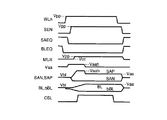
次に、前記ビット線センスアンプにおけるビット線電位の基本的なセンス動作について説明する。図18は、前記ビット線センスアンプにおけるセンス動作を示すタイミングチャートである。 Next, a basic sense operation of the bit line potential in the bit line sense amplifier will be described. FIG. 18 is a timing chart showing a sensing operation in the bit line sense amplifier.
まず、ビット線イコライズ信号BLEQの立ち下りによって、ビット線イコライズ回路108が非活性化される。その後、ワード線WLnが立ち上がると、メモリセル容量CPに蓄えられた電荷はトランジスタTRを介してビット線bBLに読み出される。仮に、蓄積されていたデータが“0”であれば、ビット線bBLの電位はイコライズ電位VBLから100mV程度低くなる。
{First, the fall of the bit line equalize signal BLEQ deactivates the bit line equalize
その後、センスイネーブル信号がSEN、SEPの順で活性化され、センスアンプ駆動信号SANが接地電位Vssに、センスアンプ駆動信号SAPが電圧Vaaに向けて変化する。信号SANの電圧低下でトランジスタT102のゲート−ソース間電圧VgsがトランジスタT102のしきい電圧Vthnよりも高くなれば、トランジスタT102がオンする。信号SAPの電圧上昇でトランジスタT103のゲート−ソース間電圧VgsがトランジスタT103のしきい電圧Vthpよりも高くなれば、トランジスタT103がオンする。これにより、ビット線bBLは接地電位Vssに向けて放電され、ビット線BLは電圧Vaaに向けて充電される。この結果、ビット線bBLに読み出された信号が増幅される。 (4) Thereafter, the sense enable signal is activated in the order of SEN and SEP, the sense amplifier drive signal SAN changes toward the ground potential Vss, and the sense amplifier drive signal SAP changes toward the voltage Vaa. When the voltage Vgs between the gate and the source of the transistor T102 becomes higher than the threshold voltage Vthn of the transistor T102 due to the voltage drop of the signal SAN, the transistor T102 is turned on. When the gate-source voltage Vgs of the transistor T103 becomes higher than the threshold voltage Vthp of the transistor T103 due to the rise in the voltage of the signal SAP, the transistor T103 is turned on. As a result, the bit line bBL is discharged toward the ground potential Vss, and the bit line BL is charged toward the voltage Vaa. As a result, the signal read to the bit line bBL is amplified.
その後、ビット線対BL、bBLに十分な電位差が生じた時点でカラム選択スイッチ109に入力されるカラム選択信号CSLが立ち上がり、データがI/O線対IO、bIOに読み出される。I/O線対へのデータ読み出し後も、メモリセルヘデータをリストアするためにビット線対BL、bBLへの充放電が継続される。
(4) Thereafter, when a sufficient potential difference occurs between the bit line pair BL and bBL, the column selection signal CSL input to the
前述した動作より、メモリセルからのデータの高速読み出し、またはメモリセルヘのデータのリストアが含まれるサイクルタイムの短縮のいずれを達成するにも、ビット線電位のセンス動作の高速化、特に初期のセンス時間の短縮が重要であることがわかる。前記ビット線電位のセンス動作を高速化するための例としては、ビット線オーバドライブ機構を設けた記憶装置が開示されている(例えば、特許文献1参照)。 According to the above-described operation, to achieve high-speed reading of data from the memory cell or shortening of the cycle time including restoration of data to the memory cell, the speed of the bit line potential sensing operation is increased, particularly the initial sensing time. It is understood that shortening is important. As an example for speeding up the bit line potential sensing operation, a storage device provided with a bit line overdrive mechanism is disclosed (for example, see Patent Document 1).
また、前述した初期のセンス時間を短縮するためには、信号SAN、SAPが流れる配線を介して接地電位Vss、電圧Vaaに流れる電流値を大きくすること、つまり信号SAN、SAPが流れる配線の配線抵抗を削減することと、信号SAN、SAPの駆動トランジスタT111、T112の寸法を大きくすることが特に有効である。そのために、センスアンプ及びセンスアンプ駆動回路のレイアウトにはさまざまな工夫がなされてきた。その一例を以下に示す。 Further, in order to shorten the initial sensing time described above, it is necessary to increase the value of the current flowing to the ground potential Vss and the voltage Vaa via the wiring through which the signals SAN and SAP flow, that is, the wiring of the wiring through which the signals SAN and SAP flow It is particularly effective to reduce the resistance and increase the dimensions of the driving transistors T111 and T112 for the signals SAN and SAP. Therefore, various ideas have been devised for the layout of the sense amplifier and the sense amplifier drive circuit. An example is shown below.
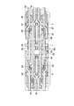
図19は、センスアンプ及びセンスアンプ駆動回路のレイアウトを示す概略図である。この図19では、センスアンプ駆動回路(SAD)111を分散配置し、センスアンプ駆動回路(SAD)111からセンスアンプ(SA1〜SA2m)106までのセンスアンプ駆動信号SAN、SAPが流れる配線の抵抗を小さくした例を示している。 FIG. 19 is a schematic diagram showing a layout of a sense amplifier and a sense amplifier drive circuit. In FIG. 19, the sense amplifier drive circuit (SAD) 111 is arranged in a distributed manner, and the resistance of the wiring through which the sense amplifier drive signals SAN and SAP flow from the sense amplifier drive circuit (SAD) 111 to the sense amplifiers (SA1 to SA2m) 106 is reduced. An example in which the size is reduced is shown.
2つのメモリセルアレイ間でセンスアンプを共有する方式の場合、4mカラムのセルアレイ105に対して左右にそれぞれ2mカラムのセンスアンプ106が配置される。ここでは、右側に配置される2mカラムのセンスアンプは図示していない。センスアンプ(SA1〜SA2m)106の列の中央には、センスアンプ駆動回路111が配置されている。このような方式では、セルアレイ105の2カラム分のピッチよりもセンスアンプの1カラムのピッチを小さくレイアウトすることにより、センスアンプ寸法を大きくすることなく、センスアンプ106の列内にもセンスアンプ駆動回路111を配置するスペースを捻出している。
しかしながら、図19に示したレイアウト方式では、センスアンプ駆動回路111のトランジスタ寸法を実際にはそれほど大きく設定することができない。さらに、セルアレイ105とセンスアンプ106間のビット線の接続が、領域W1で示すように複雑化し、ビット線の配線容量にアンバランスが生じる。したがって、このレイアウト方式は、センス動作のスピードを重視する場合には適切でない。
However, in the layout method shown in FIG. 19, the transistor dimensions of the sense
そこでこの発明は、前記課題に鑑みてなされたものであり、ビット線電位のセンス動作の高速化に適した半導体集積回路を提供することを目的とする。 Therefore, the present invention has been made in view of the above-described problems, and has as its object to provide a semiconductor integrated circuit suitable for speeding up a bit line potential sensing operation.
前記目的を達成するために、この発明の一実施形態の半導体集積回路装置は、メモリセルがマトリクス状に配置されたメモリセルアレイと、前記メモリセルから読み出された信号を増幅する、NチャネルMOSトランジスタから構成されたNチャネルセンスアンプとPチャネルMOSトランジスタから構成されたPチャネルセンスアンプとを含むセンスアンプと、前記センスアンプに隣接して配置され、前記センスアンプが含む前記Nチャネルセンスアンプ及びPチャネルセンスアンプをそれぞれ駆動するNチャネルMOSトランジスタを有する第1、第2の駆動回路と、前記第1、第2の駆動回路が有する各々の前記NチャネルMOSトランジスタのゲート電極に共通の制御信号を供給するセンスアンプ制御回路とを具備することを特徴とする。 In order to achieve the above object, a semiconductor integrated circuit device according to one embodiment of the present invention includes a memory cell array in which memory cells are arranged in a matrix, and an N-channel MOS amplifying a signal read from the memory cell. A sense amplifier including an N-channel sense amplifier including transistors and a P-channel sense amplifier including P-channel MOS transistors, the N-channel sense amplifier disposed adjacent to the sense amplifier, and included in the sense amplifier; First and second drive circuits having N-channel MOS transistors for driving P-channel sense amplifiers respectively, and a control signal common to the gate electrodes of the N-channel MOS transistors of the first and second drive circuits And a sense amplifier control circuit for supplying To.
この発明によれば、ビット線電位のセンス動作の高速化に適した半導体集積回路を提供することが可能である。 According to the present invention, it is possible to provide a semiconductor integrated circuit suitable for speeding up a bit line potential sensing operation.
この発明の実施の形態を説明する前に、センスアンプを駆動するためのセンスアンプ駆動回路をセンスアンプに隣接して配置した半導体集積回路について説明する。ここでは、半導体集積回路として、ランダムアクセスが可能なダイナミックランダムアクセスメモリ(DRAM)について述べる。 Before describing the embodiments of the present invention, a semiconductor integrated circuit in which a sense amplifier driving circuit for driving a sense amplifier is arranged adjacent to the sense amplifier will be described. Here, a random access dynamic random access memory (DRAM) will be described as a semiconductor integrated circuit.
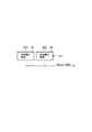
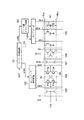
図1は、センスアンプにおけるセンス動作のスピードを重視する場合に、一般的に使用されるセンスアンプ及びセンスアンプ駆動回路のレイアウトを示す概略図である。 FIG. 1 is a schematic diagram showing a layout of a sense amplifier and a sense amplifier driving circuit which are generally used when importance is placed on the speed of the sense operation in the sense amplifier.
図1において、センスアンプ6の1カラムのピッチは、セルアレイ5の2カラム分のピッチと等しく設定する。Pチャネルセンスアンプ(PSA)が配列されるPチャネルセンスアンプ列6Pに隣接して、Pチャネルセンスアンプを駆動するためのセンスアンプ駆動回路(PSAD)11が配置される。また、Nチャネルセンスアンプ(NSA)が配列されるNチャネルセンスアンプ列6Nに隣接して、Nチャネルセンスアンプを駆動するためのセンスアンプ駆動回路(NSAD)10が配置される。
In FIG. 1, the pitch of one column of the
図2は、図1に示したレイアウトを有する半導体集積回路を、回路構成にて示した回路図である。 FIG. 2 is a circuit diagram showing a semiconductor integrated circuit having the layout shown in FIG. 1 in a circuit configuration.
図2に示すように、外部から複数の外部入力信号EXTがバッファ制御回路1へ入力される。バッファ制御回路1は、外部入力信号EXTに基づいて、ビット線センスアンプ制御信号φSA、ワード線制御信号φWL、及びロウアドレスRAを生成する。ビット線センスアンプ制御信号φSAは、センスアンプ制御回路2に入力される。ワード線制御信号φWLはワード線ドライブ回路3に入力され、ロウアドレスRAはロウデコーダ4に入力される。
(2) As shown in FIG. 2, a plurality of external input signals EXT are externally input to the
前記ロウデコーダ4からの出力信号が入力されるワード線WL1、…、WLn−1、WLnは、トランジスタTRと容量CPで構成されたメモリセルMCに接続されている。メモリセルMCは、アレイ状に複数配置されてメモリセルアレイ5を構成している。
The word lines WL1,..., WLn−1, WLn to which the output signal from the
前記メモリセルMCに記憶されたデータの読み出し、及びメモリセルMCへのデータの書き込みは、ビット線センスアンプによって制御される。ビット線センスアンプは、ダイナミック型CMOSセンスアンプ6、セルアレイ選択スイッチ7、ビット線イコライズ回路8、カラム選択スイッチ9、及びセンスアンプ駆動回路10、11で構成される。センスアンプ6は、相補関係にあるビット線対BLとbBLとの間にクロス接続されている。セルアレイ選択スイッチ7は、セルアレイ5とセンスアンプ6との間に配置されている。ビット線イコライズ回路8は、ビット線対BLとbBLを接続すると共に、これらビット線対BL、bBLを電圧Vblにプリチャージする。カラム選択スイッチ9は、カラム選択信号CSLによって制御され、データ読み出しまたは書き込みを行うビット線対BL、bBLを選択する。センスアンプ駆動回路10、11は、センスアンプ6を活性化あるいは非活性化状態にする。
{Reading of data stored in the memory cell MC and writing of data to the memory cell MC are controlled by a bit line sense amplifier. The bit line sense amplifier includes a dynamic
通常は、2つのセルアレイ間でセンスアンプ6が共有されているので、セルアレイ選択スイッチ7とビット線イコライズ回路8はセンスアンプ6を挟んで反対側にも接続されるが、ここでは図示しない。
Usually, since the
前記ダイナミック型CMOSセンスアンプ6は、NチャネルMOSトランジスタT1、T2からなるNチャネルセンスアンプと、PチャネルMOSトランジスタT3、T4からなるPチャネルセンスアンプとを有している。
The dynamic
Nチャネルセンスアンプの共通ソースには、Nチャネルセンスアンプ駆動信号SANが入力される。さらに、センスアンプ駆動信号SANは、Nチャネルセンスアンプ駆動回路10を構成するNチャネルMOSトランジスタT5のドレインに入力される。トランジスタT5のソースには接地電位Vssが供給され、ゲートにはセンスイネーブル信号SENが入力される。
N An N-channel sense amplifier drive signal SAN is input to a common source of the N-channel sense amplifier. Further, the sense amplifier drive signal SAN is input to the drain of the N-channel MOS transistor T5 included in the N-channel sense
また、Pチャネルセンスアンプの共通ソースには、Pチャネルセンスアンプ駆動信号SAPが入力される。さらに、センスアンプ駆動信号SAPは、Pチャネルセンスアンプ駆動回路11を構成するPチャネルMOSトランジスタT6のドレインに入力される。トランジスタT6のソースにはビット線リストア電位Vaaが供給され、ゲートにはセンスイネーブル信号SEPが入力される。センスアンプ駆動信号SAN、SAP、及びセンスイネーブル信号SEN、SEPは、いずれもセンスアンプ制御回路2から出力される。
(4) The P-channel sense amplifier drive signal SAP is input to the common source of the P-channel sense amplifier. Further, the sense amplifier drive signal SAP is input to the drain of the P-channel MOS transistor T6 forming the P-channel sense
図3は、前記センスアンプ制御回路2の構成を示す回路図である。
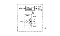
FIG. 3 is a circuit diagram showing a configuration of the sense
センスアンプ制御回路2は、タイミング発生回路21とイコライズ回路22を有する。タイミング発生回路21では、入力されるセンスアンプ制御信号φSAに基づいて、センスアンプ動作で必要な各種の制御信号SEN、SEP、SAEQを生成する。イコライズ回路22は、トランジスタT8、T9、T10からなり、制御信号SAEQを受け取り、センスアンプ駆動信号SANとSAPをイコライズする。イコライズ回路22は、センスアンプ6が非活性状態のときに、センスアンプイコライズ信号SAEQに従って、センスアンプ駆動信号SAN、SAPをイコライズ電位Vbl(Vaa/2レベル)にプリチャージする。
The sense
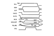
次に、基本的なビット線電位のセンス動作について図4を用いて説明する。図4は、前記ビット線センスアンプにおけるビット線電位のセンス動作を示すタイミングチャートである。 Next, a basic bit line potential sensing operation will be described with reference to FIG. FIG. 4 is a timing chart showing a bit line potential sensing operation in the bit line sense amplifier.
まず、ビット線イコライズ信号BLEQの立ち下りによって、ビット線イコライズ回路8が非活性化される。次に、ワード線WLnが立ち上がると、メモリセルの容量CPに蓄えられた電荷はトランジスタTRを介してビット線bBLに読み出される。仮に、メモリセルMCに蓄積されていたデータが“0”であれば、ビット線bBLの電位はイコライズ電位Vblから100mV程度低くなる。
{First, the falling of the bit line equalizing signal BLEQ deactivates the bit
その後、センスイネーブル信号SENが電圧Vppに向けて立ち上がり、続いてセンスイネーブル信号SEPが接地電位Vssに向けて立ち下がる。これにより、センスアンプ駆動回路(トランジスタT5、T6)が活性化される。このトランジスタT5、T6の活性化によって、センスアンプ駆動信号SANが接地電位Vssに、センスアンプ駆動信号SAPが電圧Vaaに向けて変化する。 (4) Thereafter, the sense enable signal SEN rises toward the voltage Vpp, and subsequently, the sense enable signal SEP falls toward the ground potential Vss. As a result, the sense amplifier drive circuit (transistors T5 and T6) is activated. By the activation of the transistors T5 and T6, the sense amplifier drive signal SAN changes toward the ground potential Vss, and the sense amplifier drive signal SAP changes toward the voltage Vaa.
センスアンプ駆動信号SANの電圧低下で、トランジスタT2のゲート−ソース間電圧VgsがトランジスタT2のしきい電圧Vthnよりも高くなれば、トランジスタT2がオンする。センスアンプ駆動信号SAPの電圧上昇でトランジスタT3のゲート−ソース間電圧VgsがトランジスタT3のしきい電圧Vthpよりも高くなれば、トランジスタT3がオンする。これにより、ビット線bBLは接地電位Vssに向けて放電される。また、ビット線BLは電圧Vaaに向けて充電される。この結果、ビット線bBLに読み出された信号が増幅される。 (4) If the voltage Vgs between the gate and the source of the transistor T2 becomes higher than the threshold voltage Vthn of the transistor T2 due to the voltage drop of the sense amplifier drive signal SAN, the transistor T2 turns on. When the voltage Vgs between the gate and the source of the transistor T3 becomes higher than the threshold voltage Vthp of the transistor T3 due to the rise of the voltage of the sense amplifier drive signal SAP, the transistor T3 is turned on. Thereby, the bit line bBL is discharged toward the ground potential Vss. Further, the bit line BL is charged toward the voltage Vaa. As a result, the signal read to the bit line bBL is amplified.
その後、ビット線対BLとbBLとの間に十分な電位差が生じた時点でカラム選択スイッチ9に入力されるカラム選択信号CSLが立ち上がり、データがI/O線対IO、bIOに読み出される。I/O線対へのデータ読み出し後も、メモリセルMCヘデータをリストアするためにビット線対BL、bBLへの充放電が継続される。 (4) Thereafter, when a sufficient potential difference occurs between the bit line pair BL and bBL, the column selection signal CSL input to the column selection switch 9 rises, and data is read out to the I / O line pair IO and bIO. Even after reading data to the I / O line pair, charging / discharging of the bit line pair BL and bBL is continued to restore data to the memory cell MC.
図5は、前記センスアンプ及びセンスアンプ駆動回路を構成するトランジスタの具体的なレイアウト図である。 FIG. 5 is a specific layout diagram of the transistors constituting the sense amplifier and the sense amplifier drive circuit.
この図5は、2カラム分のセンスアンプとセンスアンプ駆動回路を示している。領域CにはPチャネルセンスアンプ(トランジスタT3、T4)が配置され、領域BにはPチャネルセンスアンプ駆動回路(トランジスタT6)が配置される。また、領域EにはNチャネルセンスアンプ(トランジスタT1、T2)が配置され、領域DにはNチャネルセンスアンプ駆動回路(トランジスタT5)が配置される。領域A1、A2は、それぞれカラムごとのセンスアンプ領域を示している。 FIG. 5 shows a sense amplifier and a sense amplifier drive circuit for two columns. In a region C, a P-channel sense amplifier (transistors T3 and T4) is arranged, and in a region B, a P-channel sense amplifier driving circuit (transistor T6) is arranged. An N-channel sense amplifier (transistors T1 and T2) is arranged in the region E, and an N-channel sense amplifier driving circuit (transistor T5) is arranged in the region D. The areas A1 and A2 each indicate a sense amplifier area for each column.
図5に示すように、P型拡散領域31上には、ゲート電極32、33、ドレインコンタクト34、35、及び共通ソースコンタクト36が形成される。前記ゲート電極32、33は、クロスカップルされたPチャネルトランジスタT3、T4のそれぞれのゲート電極である。ドレインコンタクト34、35は、トランジスタT3、T4のドレインにそれぞれ接続されている。共通ソースコンタクト36は、トランジスタT3、T4の共通のソースに接続されている。
(5) As shown in FIG. 5, on the P-
トランジスタT3,T4から構成されるPチャネルセンスアンプに隣接して、センスアンプ駆動回路を構成する駆動トランジスタT6が配置される。この駆動トランジスタT6は、P型拡散領域37に形成される。P型拡散領域37上には、トランジスタT6のゲート電極38、ドレインコンタクト39、及びソースコンタクト40が形成される。なお、ゲート電極38のゲートコンタクトは図示していないが、センスアンプ領域上を縦に走る配線から、あるまとまったセンスアンプ単位ごとに取られる。
(4) A drive transistor T6 forming a sense amplifier drive circuit is arranged adjacent to the P-channel sense amplifier formed by the transistors T3 and T4. This drive transistor T6 is formed in the P-type diffusion region 37. On the P-type diffusion region 37, a
ウェル境界41は、Pチャネルセンスアンプが含まれるNウェル領域と、Nチャネルセンスアンプが含まれるPウェル領域との境界である。Pウェル領域内の領域E、Dには、前述したように、Nチャネルセンスアンプ(トランジスタT1、T2)、センスアンプ駆動回路(トランジスタT5)がそれぞれ配置される。
The
図5に示したレイアウトでは、センスアンプの2カラム当たりに1つの駆動トランジスタが隣接配置されるため、センスアンプとセンスアンプを駆動する駆動トランジスタとの間の配線抵抗を非常に小さくできる。また、センスアンプの2カラム当たりに1つ設けられる駆動トランジスタの寸法を十分大きく設定できるため、ビット線電位のセンス時間を短縮することが可能となる。 (5) In the layout shown in FIG. 5, since one drive transistor is arranged adjacent to every two columns of the sense amplifier, the wiring resistance between the sense amplifier and the drive transistor for driving the sense amplifier can be extremely reduced. In addition, since the size of one driving transistor provided for every two columns of the sense amplifier can be set sufficiently large, it is possible to shorten the bit line potential sensing time.
しかし、図5に示したレイアウトでは、センスアンプ及びセンスアンプ駆動回路を形成するために必要な領域の寸法が増え、チップサイズが大きくなってしまう。具体的には、Nチャネルセンスアンプ及びPチャネルセンスアンプのそれぞれの駆動トランジスタを、前記Nチャネルセンスアンプ及びPチャネルセンスアンプの横にそれぞれ配置したため、トランジスタ領域が増大する。さらに、センスアンプを駆動するセンスイネーブル信号SEN、SEPの配線が2本増える。これらにより、チップ面積が大幅に増大し、高速ランダムアクセスが可能なDRAMを安価に提供することができない場合がある。 However, in the layout shown in FIG. 5, the size of the region necessary for forming the sense amplifier and the sense amplifier driving circuit increases, and the chip size increases. Specifically, since the respective drive transistors of the N-channel sense amplifier and the P-channel sense amplifier are arranged beside the N-channel sense amplifier and the P-channel sense amplifier, respectively, the transistor area increases. Further, the number of wires of the sense enable signals SEN and SEP for driving the sense amplifier is increased by two. As a result, the chip area is significantly increased, and it may not be possible to provide a DRAM capable of high-speed random access at low cost.
このような問題点を解決した、この発明の実施の形態の半導体集積回路について以下に説明する。説明に際し、前述した半導体集積回路における構成と同様の部分には同じ符号を付す。 The following describes a semiconductor integrated circuit according to an embodiment of the present invention which has solved such problems. In the description, the same parts as those in the configuration of the semiconductor integrated circuit described above are denoted by the same reference numerals.
図6は、この発明の実施の形態の半導体集積回路の構成を示す回路図である。 FIG. 6 is a circuit diagram showing a configuration of a semiconductor integrated circuit according to an embodiment of the present invention.
図6に示すように、外部から複数の外部入力信号EXTがバッファ制御回路1へ入力される。バッファ制御回路1は、外部入力信号EXTに基づいて、ビット線センスアンプ制御信号φSA、ワード線制御信号φWL、及びロウアドレスRAを生成する。ビット線センスアンプ制御信号φSAは、センスアンプ制御回路2Aに入力される。ワード線制御信号φWLはワード線ドライブ回路3に入力され、ロウアドレスRAはロウデコーダ4に入力される。
(6) As shown in FIG. 6, a plurality of external input signals EXT are externally input to the
前記ロウデコーダ4からの出力信号が入力されるワード線WL1、…、WLn−1、WLnは、トランジスタTRと容量CPで構成されたメモリセルMCに接続されている。メモリセルMCは、アレイ状(例えばマトリクス状)に複数配置されてメモリセルアレイ5を構成している。
The word lines WL1,..., WLn−1, WLn to which the output signal from the
前記メモリセルMCに記憶されたデータの読み出し、及びメモリセルMCへのデータの書き込みは、ビット線センスアンプによって制御される。ビット線センスアンプは、ダイナミック型CMOSセンスアンプ6、セルアレイ選択スイッチ7、ビット線イコライズ回路8、カラム選択スイッチ9、及びセンスアンプ駆動回路10、11Aで構成される。センスアンプ6は、相補関係にあるビット線対BLとbBLとの間にクロス接続されている。セルアレイ選択スイッチ7は、セルアレイ5とセンスアンプ6との間に配置されている。ビット線イコライズ回路8は、ビット線対BLとbBLを接続すると共に、これらビット線対BL、bBLを電圧Vblにプリチャージする。カラム選択スイッチ9は、カラム選択信号CSLによって制御され、データ読み出しまたは書き込みを行うビット線対BL、bBLを選択する。センスアンプ駆動回路10、11Aは、センスアンプ6を活性化あるいは非活性化状態にする。
{Reading of data stored in the memory cell MC and writing of data to the memory cell MC are controlled by a bit line sense amplifier. The bit line sense amplifier includes a dynamic
通常は、2つのセルアレイ間でセンスアンプ6が共有されているので、セルアレイ選択スイッチ7とビット線イコライズ回路8はセンスアンプ6を挟んで反対側にも接続されるが、ここでは図示しない。
Usually, since the
前記ダイナミック型CMOSセンスアンプ6は、NチャネルMOSトランジスタT1、T2からなるNチャネルセンスアンプと、PチャネルMOSトランジスタT3、T4からなるPチャネルセンスアンプとを有している。
The dynamic
Nチャネルセンスアンプの共通ソースには、Nチャネルセンスアンプ駆動信号SANが入力される。さらに、センスアンプ駆動信号SANは、Nチャネルセンスアンプ駆動回路10を構成するNチャネルMOSトランジスタT5のドレインに入力される。トランジスタT5のソースには接地電位Vssが供給され、ゲートにはセンスイネーブル信号SENが入力される。
N An N-channel sense amplifier drive signal SAN is input to a common source of the N-channel sense amplifier. Further, the sense amplifier drive signal SAN is input to the drain of the N-channel MOS transistor T5 included in the N-channel sense
また、Pチャネルセンスアンプの共通ソースには、Pチャネルセンスアンプ駆動信号SAPが入力される。さらに、センスアンプ駆動信号SAPは、Pチャネルセンスアンプ駆動回路11Aを構成するNチャネルMOSトランジスタT7のドレインに入力される。トランジスタT7のソースにはビット線リストア電位Vaaが供給され、ゲートには前記トランジスタT5のゲートと同様に、センスイネーブル信号SENが入力される。センスアンプ駆動信号SAN、SAP、及びセンスイネーブル信号SENは、いずれもセンスアンプ制御回路2Aから出力される。
(4) The P-channel sense amplifier drive signal SAP is input to the common source of the P-channel sense amplifier. Further, the sense amplifier drive signal SAP is input to the drain of the N-channel MOS transistor T7 forming the P-channel sense
図1に示した半導体集積回路とは、Pチャネルセンスアンプを駆動するセンスアンプ駆動回路がNチャネルMOSトランジスタT7で構成される点と、Nチャネル及びPチャネルセンスアンプを駆動するセンスアンプ駆動回路、すなわちトランジスタT5及びT7のゲートに入力される信号が同一のセンスイネーブル信号SENである点が異なっている。 The semiconductor integrated circuit shown in FIG. 1 is different from the semiconductor integrated circuit shown in FIG. 1 in that a sense amplifier drive circuit for driving a P-channel sense amplifier is constituted by an N-channel MOS transistor T7, That is, the difference is that the signals input to the gates of the transistors T5 and T7 are the same sense enable signal SEN.
図7は、前記センスアンプ制御回路2Aの構成を示す回路図である。
FIG. 7 is a circuit diagram showing a configuration of the sense
センスアンプ制御回路2Aは、タイミング発生回路21とイコライズ回路22を有する。タイミング発生回路21では、入力されるセンスアンプ制御信号φSAに基づいて、センスアンプ動作で必要な各種の制御信号SEN、SAEQを生成する。イコライズ回路22は、トランジスタT8、T9、T10からなり、制御信号SAEQを受け取り、センスアンプ駆動信号SANとSAPをイコライズする。イコライズ回路22は、センスアンプ6が非活性状態のときに、センスアンプイコライズ信号SAEQに従って、センスアンプ駆動信号SAN、SAPをイコライズ電位Vbl(Vaa/2レベル)にプリチャージする。
The sense
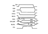
次に、基本的なビット線電位のセンス動作について図8を用いて説明する。図8は、前記ビット線センスアンプにおけるビット線電位のセンス動作を示すタイミングチャートである。 Next, a basic bit line potential sensing operation will be described with reference to FIG. FIG. 8 is a timing chart showing a bit line potential sensing operation in the bit line sense amplifier.
まず、ビット線イコライズ信号BLEQの立ち下りによって、ビット線イコライズ回路8が非活性化される。次に、ワード線WLnが立ち上がると、メモリセルの容量CPに蓄えられた電荷はトランジスタTRを介してビット線bBLに読み出される。仮に、メモリセルMCに蓄積されていたデータが“0”であれば、ビット線bBLの電位はイコライズ電位Vblから100mV程度低くなる。
{First, the falling of the bit line equalizing signal BLEQ deactivates the bit
その後、センスイネーブル信号SENが電圧Vppに向けて立ち上がり、センスアンプ駆動回路(トランジスタT5、T7)が活性化される。これにより、センスアンプ駆動信号SANが接地電位Vssに向けて変化する。これと同時に、センスアンプ駆動信号SAPがビット線リストア電位Vaaに向けて変化する。 (4) Thereafter, the sense enable signal SEN rises toward the voltage Vpp, and the sense amplifier driving circuits (transistors T5 and T7) are activated. As a result, the sense amplifier drive signal SAN changes toward the ground potential Vss. At the same time, the sense amplifier drive signal SAP changes toward the bit line restore potential Vaa.
この実施の形態では、ビット線リストア速度のさらなる高速化のために、すなわちビット線BLを電圧Vaaまで充電する速度を高速化するために、ビット線電位のセンス動作の初期に、ビット線リストア電位Vaaを一時的に電圧Vaahまで上昇させるオーバードライブ方式を採用している。前記電圧Vaahは、電圧Vaaより所定電圧だけ高い電圧である。 In this embodiment, in order to further increase the bit line restore speed, that is, to increase the speed at which the bit line BL is charged to the voltage Vaa, the bit line restore potential is set at the beginning of the bit line potential sense operation. An overdrive method of temporarily increasing Vaa to a voltage Vaah is employed. The voltage Vaah is a voltage higher than the voltage Vaa by a predetermined voltage.
Nチャネル及びPチャネルセンスアンプを駆動する駆動トランジスタT5及びT7のゲートには、前述したように、センスイネーブル信号SENが共通に入力される。このとき、トランジスタT7のソース電位の初期値はイコライズ電位Vblと高い。このため、Pチャネルセンスアンプ駆動信号SAPの立ち上がりは、Nチャネルセンスアンプ駆動信号SANの立ち下がりよりもわずかに遅くなる。 As described above, the sense enable signal SEN is commonly input to the gates of the driving transistors T5 and T7 that drive the N-channel and P-channel sense amplifiers. At this time, the initial value of the source potential of the transistor T7 is as high as the equalizing potential Vbl. Therefore, the rise of the P-channel sense amplifier drive signal SAP is slightly later than the fall of the N-channel sense amplifier drive signal SAN.
センスアンプ駆動信号SANの電圧低下で、トランジスタT2のゲート−ソース間電圧Vgsがしきい電圧Vthnよりも高くなればトランジスタT2がオンする。また、センスアンプ駆動信号SAPの電圧上昇で、トランジスタT3のゲート−ソース間電圧Vgsがしきい電圧Vthpよりも高くなればトランジスタT3がオンする。これらにより、ビット線bBLは接地電位Vssに向けて放電され、ビット線BLは電圧Vaahに向けて充電される。この結果、ビット線bBLに読み出された信号が増幅される。 (4) When the voltage Vgs between the gate and the source of the transistor T2 becomes higher than the threshold voltage Vthn due to the voltage drop of the sense amplifier drive signal SAN, the transistor T2 is turned on. When the voltage Vgs between the gate and the source of the transistor T3 becomes higher than the threshold voltage Vthp due to the rise of the voltage of the sense amplifier drive signal SAP, the transistor T3 is turned on. As a result, the bit line bBL is discharged toward the ground potential Vss, and the bit line BL is charged toward the voltage Vaah. As a result, the signal read to the bit line bBL is amplified.
その後、ビット線対BLとbBLとの間に十分な電位差が生じた時点でカラム選択スイッチ9に入力されるカラム選択信号CSLが立ち上がり、データがI/O線対IO、bIOに読み出される。I/O線対へのデータ読み出し後も、メモリセルヘデータをリストアするためにビット線対BL、bBLへの充放電が継続される。なお、前記オーバードライブは、ビット線が予め設定されたリストア用の電圧Vaaに十分近づいた時点で停止される。 (4) Thereafter, when a sufficient potential difference occurs between the bit line pair BL and bBL, the column selection signal CSL input to the column selection switch 9 rises, and data is read out to the I / O line pair IO and bIO. Even after reading data to the I / O line pair, charging / discharging of the bit line pair BL and bBL is continued to restore data to the memory cell. Note that the overdrive is stopped when the bit line sufficiently approaches a preset restoration voltage Vaa.
図9は、前記ビット線リストア電位Vaa及び電圧Vaahを発生するオーバードライブ回路の構成を示す図である。 FIG. 9 is a diagram showing a configuration of an overdrive circuit that generates the bit line restore potential Vaa and the voltage Vaah.
このオーバードライブ回路は、チップ内に設けられており、第1内部降圧回路51、及び第2内部降圧回路52を有する。第1内部降圧回路51は、供給される電源電位Vccを降圧して、あらかじめ設定されたリストア電位Vaaを定常的に発生する。また、第2内部降圧回路52は、供給される電源電位Vccを降圧してオーバードライブ用電位を発生する。この第2内部降圧回路52には制御信号ODが入力されており、第2内部降圧回路52は制御信号ODに従って、オーバードライブ用電圧を出力するか否かを切り換える。電位Vaaより所定電圧だけ高い電圧Vaahは、ビット線リストア電位Vaaにオーバードライブ用電位を加えることにより生成される。そして、第2内部降圧回路52に入力される制御信号ODによって、電圧Vaahを出力するか否かが制御される。
This overdrive circuit is provided in the chip, and has a first internal voltage down
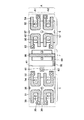
図10は、前記センスアンプ及びセンスアンプ駆動回路を構成するトランジスタの第1例のレイアウト図である。 FIG. 10 is a layout diagram of a first example of transistors constituting the sense amplifier and the sense amplifier drive circuit.
この図10には、2カラム分のセンスアンプとセンスアンプ駆動回路が示されている。領域CにはPチャネルセンスアンプ(トランジスタT3、T4)が配置され、領域EにはNチャネルセンスアンプ(トランジスタT1、T2)が配置されている。領域Fには、Nチャネルセンスアンプを駆動するセンスアンプ駆動回路(トランジスタT5)と、Pチャネルセンスアンプを駆動するセンスアンプ駆動回路(トランジスタT7)が配置されている。領域A1、A2は、それぞれカラムごとのセンスアンプ領域を示している。 FIG. 10 shows two columns of sense amplifiers and sense amplifier drive circuits. In a region C, a P-channel sense amplifier (transistors T3 and T4) is arranged, and in a region E, an N-channel sense amplifier (transistors T1 and T2) is arranged. In region F, a sense amplifier driving circuit (transistor T5) for driving an N-channel sense amplifier and a sense amplifier driving circuit (transistor T7) for driving a P-channel sense amplifier are arranged. The areas A1 and A2 each indicate a sense amplifier area for each column.
前記レイアウト図中の個々の構成について、以下に詳しく述べる。P型拡散領域31上には、ゲート電極32、33、ドレインコンタクト34、35、及び共通ソースコンタクト36が形成される。前記ゲート電極32、33は、クロスカップルされたPチャネルトランジスタT3、T4のゲート電極である。ドレインコンタクト34、35は、トランジスタT3、T4のドレインにそれぞれ接続されている。共通ソースコンタクト36は、トランジスタT3、T4の共通のソースに接続されている。N型拡散領域61及びコンタクト62は、Pチャネルセンスアンプが含まれるNウェル領域の電位を取るためのものである。
(4) Each configuration in the layout diagram will be described in detail below.
ウェル境界41は、Pチャネルセンスアンプが含まれるNウェル領域と、Nチャネルセンスアンプが含まれるPウェル領域との境界である。
The
前記Pウェル領域内のN型拡散領域42上には、ゲート電極43、44、ドレインコンタクト45、46、及び共通ソースコンタクト47が形成される。前記ゲート電極43、44は、クロスカップルされたNチャネルトランジスタT1、T2のゲート電極である。ドレインコンタクト45、46は、トランジスタT1、T2のドレインにそれぞれ接続されている。共通ソースコンタクト47は、トランジスタT1、T2の共通のソースに接続されている。
(4)
また、前記Pウェル領域内の領域Fには、センスアンプ駆動回路を構成するNチャネルMOSトランジスタT5、T7が形成されている。ここで、図6の回路図に示したように、Nチャネルセンスアンプ及びPチャネルセンヌアンプは、共にNチャンネルMOSトランジスタで駆動される。さらに、トランジスタT5、T7のゲートに入力される信号は、共にセンスイネーブル信号SENである。このような回路構成の場合、トランジスタT5及びT7をセンスアンプ6が形成される領域C、Eに隣接する領域Fに1列に配置することが可能である。
{Circle around (2)} In a region F in the P-well region, N-channel MOS transistors T5 and T7 constituting a sense amplifier driving circuit are formed. Here, as shown in the circuit diagram of FIG. 6, both the N-channel sense amplifier and the P-channel Senne amplifier are driven by N-channel MOS transistors. Further, the signals input to the gates of the transistors T5 and T7 are both sense enable signals SEN. In the case of such a circuit configuration, the transistors T5 and T7 can be arranged in one column in the region F adjacent to the regions C and E where the
N型拡散領域63上には、Pチャネルセンスアンプを駆動するための前記NチャネルトランジスタT7が形成されており、ゲート電極64、ソースコンタクト65、及びドレインコンタクト66が配置されている。ソースコンタクト65はトランジスタT7のソースに接続されており、このソースコンタクト65には電位Vaaが供給される。ドレインコンタクト66はトランジスタT7のドレインに接続されており、このドレインコンタクト66にはセンスアンプ駆動信号SAPが供給される。
On the N-
N型拡散領域67上には、Nチャネルセンスアンプを駆動するためのNチャネルトランジスタT5が形成されており、ゲート電極64、ソースコンタクト68、及びドレインコンタクト69が配置されている。図に示したトランジスタT5はレイアウトの境界部のため、トランジスタの上部と下部が分離されて描かれている。ソースコンタクト68はトランジスタT5のソースに接続されており、このソースコンタクト68には接地電位Vssが供給される。ドレインコンタクト69はトランジスタT5のドレインに接続されており、このドレインコンタクト69には信号SANが供給される。これらのトランジスタT5、T7では、チャネルイオン注入の境界と拡散領域間の余裕を取ることが難しい。このため、通常、トランジスタT5とT7のしきい値電圧は、等しく低い電圧に設定される。また、トランジスタT5とT7のゲート長は等しく設定される。
On the N-
図11は、図10に示したレイアウト図に、ビット線配線とこのビット線配線と同層の配線層を追加した図である。 FIG. 11 is a diagram in which bit line wiring and a wiring layer of the same layer as the bit line wiring are added to the layout diagram shown in FIG.
Pチャネルセンスアンプ駆動回路を構成するトランジスタT7のドレインコンタクト66と、Pチャネルセンスアンプを構成するトランジスタT3、T4の共通のソースコンタクト36は、配線81で相互に接続される。Pチャネルセンスアンプが含まれるNウェル領域に接続されたコンタクト62は、前記配線81に接続されている。配線81は、例えばタングステン(W)により形成する。
(4) The
また、Nチャネルセンスアンプ駆動回路を構成するトランジスタT5のドレインコンタクト69と、Nチャネルセンスアンプを構成するトランジスタT1、T2の共通のソースコンタクト47は、配線82で相互に接続される。配線81と配線82は、図11に示すように、列方向に交互に配置される。なお、ビット線と同じ配線層で直接接続されていないソースコンタクト36、47もあるが、ソースコンタクト36間、及びソースコンタクト47間はさらに前記配線81、82より上層の配線層を介してそれぞれ共通に接続される。
The
また、トランジスタT4のドレインコンタクト35、トランジスタT3のゲート電極32、トランジスタT2のドレインコンタクト46、及びトランジスタT1のゲート電極43は、ビット線bBLである配線83で相互に接続される。トランジスタT3のドレインコンタクト34、トランジスタT4のゲート電極33、トランジスタT1のドレインコンタクト45、及びトランジスタT2のゲート電極44は、ビット線BLである配線84で相互に接続される。
{The
図12は、前記センスアンプ及びセンスアンプ駆動回路を構成するトランジスタの第2例のレイアウト図である。 FIG. 12 is a layout diagram of a second example of the transistors constituting the sense amplifier and the sense amplifier drive circuit.
この図12には、前記第1例と同様に、2カラム分のセンスアンプとセンスアンプ駆動回路が示されている。領域CにはPチャネルセンスアンプ(トランジスタT3、T4)が配置され、領域EにはNチャネルセンスアンプ(トランジスタT1、T2)が配置されている。領域Fには、Nチャネルセンスアンプを駆動するセンスアンプ駆動回路(トランジスタT5)、またはPチャネルセンスアンプを駆動するセンスアンプ駆動回路(トランジスタT7)が配置されている。領域A1、A2は、それぞれカラムごとのセンスアンプ領域を示している。 FIG. 12 shows a sense amplifier and a sense amplifier drive circuit for two columns, as in the first example. In a region C, a P-channel sense amplifier (transistors T3 and T4) is arranged, and in a region E, an N-channel sense amplifier (transistors T1 and T2) is arranged. In the region F, a sense amplifier driving circuit (transistor T5) for driving an N-channel sense amplifier or a sense amplifier driving circuit (transistor T7) for driving a P-channel sense amplifier is arranged. The areas A1 and A2 each indicate a sense amplifier area for each column.
前記レイアウト図中の個々の構成について、以下に詳しく述べる。P型拡散領域31上には、前記第1例と同様に、ゲート電極32、33、ドレインコンタクト34、35、及び共通ソースコンタクト36が形成されている。N型拡散領域61及びコンタクト62は、Pチャネルセンスアンプが含まれるN型ウェル領域の電位を設定するためのものである。さらに、ウェル境界41は、Pチャネルセンスアンプが含まれるN型ウェル領域と、Nチャネルセンスアンプが含まれるP型ウェル領域との境界である。
(4) Each configuration in the layout diagram will be described in detail below.
前記P型ウェル領域内のN型拡散領域42上には、ゲート電極93、94、ドレインコンタクト95、96、及び共通ソースコンタクト97が形成される。前記ゲート電極93、94は、クロスカップルされたNチャネルトランジスタT1、T2のゲート電極である。ドレインコンタクト95、96は、トランジスタT1、T2のドレインにそれぞれ接続されている。共通ソースコンタクト97は、トランジスタT1、T2の共通のソースに接続されている。
(4)
また、前記P型ウェル領域内の領域Fには、センスアンプ駆動回路を構成するNチャネルMOSトランジスタT5またはT7が形成されており、ゲート電極98が配置されている。NチャネルMOSトランジスタT5またはT7のゲート電極98の一端は、領域Aの末端まで延伸されずに切断されている。一方、ゲート電極98の他端には配線99が接続され、配線99にはコンタクト92が接続されている。
{Circle around (2)} In the region F in the P-type well region, an N-channel MOS transistor T5 or T7 constituting a sense amplifier driving circuit is formed, and a
図13は、図12に示したレイアウト図に、ビット線配線とこのビット線配線と同層の配線層を追加した図であり、領域FにはPチャネルセンスアンプを駆動するNチャネルMOSトランジスタT7が配置されている。 FIG. 13 is a diagram in which a bit line wiring and a wiring layer of the same layer as the bit line wiring are added to the layout diagram shown in FIG. 12, and an N-channel MOS transistor T7 driving a P-channel sense amplifier is provided in a region F. Is arranged.
N型拡散領域63上には、Pチャネルセンスアンプを駆動するための前記NチャネルトランジスタT7が形成されており、ゲート電極98、ソースコンタクト65、及びドレインコンタクト66が配置されている。
On the N-
NチャネルMOSトランジスタT7のドレインコンタクト66と、Pチャネルセンスアンプを構成するトランジスタT3、T4の共通のソースコンタクト36は、配線81で相互に接続される。Pチャネルセンスアンプが含まれるN型ウェル領域に接続されたコンタクト62は、前記配線81に接続されている。配線81は、例えばタングステン(W)により形成される。なお、ビット線と同じ配線層で直接接続されていないソースコンタクト36、97もあるが、ソースコンタクト36間、及びソースコンタクト97間はさらに前記配線81より上層の配線層を介してそれぞれ共通に接続される。
(4) The
また、トランジスタT4のドレインコンタクト35、トランジスタT3のゲート電極32、トランジスタT1のゲート電極93、及びトランジスタT2のドレインコンタクト96は、ビット線bBLである配線90で相互に接続される。トランジスタT4のゲート電極33、トランジスタT3のドレインコンタクト34、トランジスタT1のドレインコンタクト95、及びトランジスタT2のゲート電極94は、ビット線BLである配線91で相互に接続される。
{The
ソースコンタクト65はトランジスタT7のソースに接続されており、このソースコンタクト65には電位Vaaが供給される。ドレインコンタクト66はトランジスタT7のドレインに接続されており、このドレインコンタクト66にはセンスアンプ駆動信号SAPが供給される。
The
図14は、図12に示したレイアウト図に、ビット線配線とこのビット線配線と同層の配線層を追加した図であり、領域FにはNチャネルセンスアンプを駆動するNチャネルMOSトランジスタT5が配置されている。 FIG. 14 is a diagram in which a bit line wiring and a wiring layer of the same layer as the bit line wiring are added to the layout diagram shown in FIG. 12, and an N-channel MOS transistor T5 driving an N-channel sense amplifier is provided in a region F. Is arranged.
N型拡散領域63上には、Nチャネルセンスアンプを駆動するための前記NチャネルトランジスタT5が形成されており、ゲート電極98、ソースコンタクト68、及びドレインコンタクト69が配置されている。
The N-channel transistor T5 for driving the N-channel sense amplifier is formed on the N-
NチャネルMOSトランジスタT5のドレインコンタクト69と、Nチャネルセンスアンプを構成するトランジスタT1、T2の共通のソースコンタクト97は、配線82で相互に接続される。配線82は、例えばタングステン(W)により形成される。また、Pチャネルセンスアンプを構成するトランジスタT3、T4の共通のソースコンタクト36とPチャネルセンスアンプが含まれるN型ウェル領域に接続されたコンタクト62は、配線89にて接続されている。なお、ビット線と同じ配線層で直接接続されていないソースコンタクト36、97もあるが、ソースコンタクト36間、及びソースコンタクト97間はさらに前記配線81、89より上層の配線層を介してそれぞれ共通に接続される。
(4) The
また、トランジスタT4のドレインコンタクト35、トランジスタT3のゲート電極32、トランジスタT1のゲート電極93、及びトランジスタT2のドレインコンタクト96は、ビット線bBLである配線90で相互に接続される。トランジスタT4のゲート電極33、トランジスタT3のドレインコンタクト34、トランジスタT1のドレインコンタクト95、及びトランジスタT2のゲート電極94は、ビット線BLである配線91で相互に接続される。
{The
ソースコンタクト68はトランジスタT5のソースに接続されており、このソースコンタクト68には接地電位Vssが供給される。ドレインコンタクト69はトランジスタT5のドレインに接続されており、このドレインコンタクト69にはセンスアンプ駆動信号SANが供給される。
The
ここで、図6の回路図に示したように、Nチャネルセンスアンプ及びPチャネルセンヌアンプは、共にNチャンネルMOSトランジスタで駆動される。さらに、トランジスタT5またはT7のゲートに入力される信号は、共にセンスイネーブル信号SENである。このような回路構成の場合、トランジスタT5またはT7を、センスアンプ6が形成される領域C、Eに隣接する領域Fに1列に配置することが可能である。
Here, as shown in the circuit diagram of FIG. 6, both the N-channel sense amplifier and the P-channel Senne amplifier are driven by N-channel MOS transistors. Further, the signals input to the gates of the transistors T5 and T7 are both sense enable signals SEN. In the case of such a circuit configuration, it is possible to arrange the transistors T5 or T7 in a row in a region F adjacent to the regions C and E where the
また、図13、図14に示したレイアウトを用いると、Pチャネルセンスアンプ(トランジスタT3、T4)及びNチャネルセンスアンプ(トランジスタT1、T2)にセンスアンプ駆動回路(トランジスタT7またはT5)をそれぞれ接続することが可能である。半導体基板上の所定領域内に、図13及び図14に示したレイアウトを所望の数だけ配置することにより、トランジスタT7を合せたトランジスタサイズと、トランジスタT5を合せたトランジスタサイズとのサイズ比を自由に設定することができる。例えば、セルアレイとして4mカラムのメモリセルが配置される場合、計m個のセンスアンプ駆動回路(トランジスタT7またはT5)を領域Fの列に配置できる。図13に示したレイアウトをi個配置し、図14に示したレイアウトをj個配置すると、i+j=mとなる(i、jは、1、2、…、m−1)。このように図13に示したレイアウトと、図14に示したレイアウトとの配置数を調節することで、トランジスタT7及びT5(センスアンプ駆動回路)のトランジスタサイズを最適なサイズに設定する。これにより、ビット線センスの高速化とビット線リストアの高速化が容易となる。 When the layouts shown in FIGS. 13 and 14 are used, a sense amplifier driving circuit (transistor T7 or T5) is connected to a P-channel sense amplifier (transistors T3 and T4) and an N-channel sense amplifier (transistors T1 and T2). It is possible to do. By arranging a desired number of the layouts shown in FIGS. 13 and 14 in a predetermined region on the semiconductor substrate, the size ratio between the transistor size including the transistor T7 and the transistor size including the transistor T5 can be freely set. Can be set to For example, when 4 m columns of memory cells are arranged as a cell array, a total of m sense amplifier driving circuits (transistors T7 or T5) can be arranged in the column of the region F. When i layouts shown in FIG. 13 are arranged and j layouts shown in FIG. 14 are arranged, i + j = m (i, j is 1, 2,..., M-1). In this way, by adjusting the number of layouts shown in FIG. 13 and the layout shown in FIG. 14, the transistor sizes of the transistors T7 and T5 (sense amplifier drive circuit) are set to optimal sizes. This facilitates speeding up bit line sensing and speeding up bit line restoration.
図15は、図7に示した信号SAPとSANをイコライズするトランジスタT10を、図12に示した領域Fに配置したレイアウト図である。 FIG. 15 is a layout diagram in which the transistor T10 for equalizing the signals SAP and SAN shown in FIG. 7 is arranged in the region F shown in FIG.
N型拡散領域63上には、信号SAPとSANをイコライズするNチャネルMOSトランジスタT10が形成されており、ゲート電極78、ソースコンタクト85、及びドレインコンタクト86が配置されている。NチャネルMOSトランジスタT10のゲート電極78の一端は、領域Aの末端まで延伸されずに切断されている。一方、ゲート電極78の他端には配線79が接続され、配線79にはコンタクト80が接続されている。
On the N-
NチャネルMOSトランジスタT10のドレインコンタクト86と、Pチャネルセンスアンプを構成するトランジスタT3、T4の共通のソースコンタクト36は、配線87で相互に接続される。Pチャネルセンスアンプが含まれるN型ウェル領域に接続されたコンタクト62は、前記配線87に接続されている。また、NチャネルMOSトランジスタT10のソースコンタクト85と、Nチャネルセンスアンプを構成するトランジスタT1、T2の共通のソースコンタクト97は、配線88で相互に接続される。配線87、88は、例えばタングステン(W)により形成される。なお、図15に示した配線層で直接接続されていないソースコンタクト36、97もあるが、ソースコンタクト36間、及びソースコンタクト97間はさらに前記配線87、88より上層の配線層を介してそれぞれ共通に接続される。
(4) The
前記イコライズトランジスタT10のゲート電極78には、図8に示した信号SAEQが入力される。このイコライズトランジスタT10を領域Fの列方向に分散配置することにより、信号SAPとSANをイコライズするための機能を大きくすると共に配線抵抗を低減することができ、イコライズ動作を高速化できる。この結果、半導体集積回路における読み出し及び書き込みのサイクル時間(tRC)を短縮することができる。
The signal SAEQ shown in FIG. 8 is input to the
図5に示したレイアウト例では、Pチャネルセンスアンプ及びセンスアンプ駆動回路を構成するトランジスタT3、T4、及びT6が同一のNウェル領域内に形成される。このため、前記Nウェル領域の電位は電圧Vaa以下にすることはできない。したがって、図5に示したレイアウト例では、Pチャネルセンスアンプの動作開始時には、トランジスタT3、T4のソース電位は電圧Vaaよりも低くなるので、センスアンプ駆動回路(トランジスタT6)にはバックバイアスがかかる。このため、トランジスタT6のしきい電圧Vthが上昇しその駆動力が低下する。この結果、Pチャネルセンスアンプによる初期のセンス速度が悪化することがある。 In the layout example shown in FIG. 5, the transistors T3, T4, and T6 forming the P-channel sense amplifier and the sense amplifier driving circuit are formed in the same N-well region. Therefore, the potential of the N well region cannot be lower than the voltage Vaa. Therefore, in the layout example shown in FIG. 5, at the start of the operation of the P-channel sense amplifier, the source potential of the transistors T3 and T4 becomes lower than the voltage Vaa, so that a back bias is applied to the sense amplifier drive circuit (transistor T6). . For this reason, the threshold voltage Vth of the transistor T6 increases, and its driving force decreases. As a result, the initial sensing speed of the P-channel sense amplifier may deteriorate.
これに対して、この実施の形態では、Pチャネルセンスアンプによる初期のセンス動作時に、センスアンプ駆動回路(トランジスタT7)にバックバイアスがかからないため、しきい電圧Vthが低いままである。これにより、Pチャネルセンスアンプによる初期のセンス速度を高速化できる。 In contrast, in this embodiment, the threshold voltage Vth remains low because no back bias is applied to the sense amplifier driving circuit (transistor T7) during the initial sensing operation by the P-channel sense amplifier. Thereby, the initial sensing speed by the P-channel sense amplifier can be increased.
以上説明したようにこの発明の実施の形態では、レイアウト及び回路の改良により、ビット線センスアンプ活性化回路をセンスアンプに隣接して配置した場合でも従来よりもチップ面積を小さくすることができ、高速なランダムアクセスが可能なDRAMを安価に提供することができる。 As described above, in the embodiment of the present invention, the chip area can be made smaller than that of the related art even when the bit line sense amplifier activation circuit is arranged adjacent to the sense amplifier by improving the layout and the circuit. A DRAM capable of high-speed random access can be provided at low cost.
詳述すると、前記実施の形態では、従来はPチャネルMOSトランジスタで構成されていた、Pチャネルセンスアンプを駆動する第1駆動トランジスタを、NチャネルMOSトランジスタに置き換える。さらに、Nチャネルセンスアンプを駆動する第2駆動トランジスタのゲートと、前記第1駆動トランジスタのゲートへの入力信号を共通化する。これらにより、センスアンプ中に2列必要であった第1駆動トランジスタ及び第2駆動トランジスタを1列に配列することが可能であり、従来に比べてチップ面積が大幅に小さい高速なDRAMを実現できる。また、Pチャネルセンスアンプが含まれるNウェル領域の電位を、Pチャネルセンスアンプを駆動する第2駆動トランジスタの出力から取ることにより、従来に比べて初期のセンス速度を高速化することができる。 Specifically, in the above-described embodiment, the first drive transistor for driving the P-channel sense amplifier, which has conventionally been constituted by a P-channel MOS transistor, is replaced with an N-channel MOS transistor. Further, the input signal to the gate of the second drive transistor for driving the N-channel sense amplifier and the input signal to the gate of the first drive transistor are shared. As a result, the first drive transistor and the second drive transistor, which required two columns in the sense amplifier, can be arranged in one column, and a high-speed DRAM having a significantly smaller chip area than that of the related art can be realized. . Further, by obtaining the potential of the N-well region including the P-channel sense amplifier from the output of the second drive transistor for driving the P-channel sense amplifier, the initial sensing speed can be increased as compared with the related art.
また、この発明の実施の形態は前述した構成に限定されるわけではなく、前記構成の変更あるいは各種構成の追加によって、様々な実施の形態を形成することが可能である。 The embodiments of the present invention are not limited to the above-described configurations, and various embodiments can be formed by changing the configurations or adding various configurations.
1…バッファ制御回路、2、2A…センスアンプ制御回路、3…ワード線ドライブ回路、4…ロウデコーダ、5…メモリセルアレイ、6…ダイナミック型CMOSセンスアンプ、7…セルアレイ選択スイッチ、8…ビット線イコライズ回路、9…カラム選択スイッチ、10…Nチャネルセンスアンプ駆動回路、11、11A…Pチャネルセンスアンプ駆動回路、21…タイミング発生回路、22…イコライズ回路、31…P型拡散領域、32、33…ゲート電極、34、35…ドレインコンタクト、36…共通ソースコンタクト、41…ウェル境界、42…N型拡散領域、43、44…ゲート電極、45、46…ドレインコンタクト、47…共通ソースコンタクト、51…第1内部降圧回路、52…第2内部降圧回路、61…N型拡散領域、62…コンタクト、63…N型拡散領域、64…ゲート電極、65…ソースコンタクト、66…ドレインコンタクト、67…N型拡散領域、68…ソースコンタクト、69…ドレインコンタクト、78…ゲート電極、79…配線、80…コンタクト、81、82、83、84…配線、85…ソースコンタクト、86…ドレインコンタクト、87、88、89、90、91…配線、92…コンタクト、93、94…ゲート電極、95、96…ドレインコンタクト、97…共通ソースコンタクト、98…ゲート電極、99…配線、BL、bBL…ビット線対、CSL…カラム選択信号、EXT…外部入力信号、MC…メモリセル、RA…ロウアドレス、SAN…Nチャネルセンスアンプ駆動信号、SAP…Pチャネルセンスアンプ駆動信号、SEN…センスイネーブル信号、T1、T2…NチャネルMOSトランジスタ、T3、T4…PチャネルMOSトランジスタ、T5…NチャネルMOSトランジスタ、T6…PチャネルMOSトランジスタ、T7…NチャネルMOSトランジスタ、WL1、…、WLn−1、WLn…ワード線、φSA…ビット線センスアンプ制御信号、φWL…ワード線制御信号
DESCRIPTION OF
Claims (16)
前記メモリセルから読み出された信号を増幅する、NチャネルMOSトランジスタから構成されたNチャネルセンスアンプとPチャネルMOSトランジスタから構成されたPチャネルセンスアンプとを含むセンスアンプと、
前記センスアンプに隣接して配置され、前記センスアンプが含む前記Nチャネルセンスアンプ及びPチャネルセンスアンプをそれぞれ駆動するNチャネルMOSトランジスタを有する第1、第2の駆動回路と、
前記第1、第2の駆動回路が有する各々の前記NチャネルMOSトランジスタのゲート電極に共通の制御信号を供給するセンスアンプ制御回路と、
を具備することを特徴とする半導体集積回路。 A memory cell array in which memory cells are arranged in a matrix,
A sense amplifier for amplifying a signal read from the memory cell, the sense amplifier including an N-channel sense amplifier including an N-channel MOS transistor and a P-channel sense amplifier including a P-channel MOS transistor;
First and second drive circuits arranged adjacent to the sense amplifier and having N-channel MOS transistors for driving the N-channel sense amplifier and the P-channel sense amplifier included in the sense amplifier, respectively;
A sense amplifier control circuit for supplying a common control signal to a gate electrode of each of the N-channel MOS transistors of the first and second drive circuits;
A semiconductor integrated circuit comprising:
前記列方向に連続して配置され、前記メモリセルから読み出され前記ビット線対間に現われた微小信号を増幅する、PチャネルMOSトランジスタから構成されたPチャネルセンスアンプを含むセンスアンプと、
前記センスアンプに隣接して前記列方向に連続して配置され、前記センスアンプが含む前記Pチャネルセンスアンプを駆動するNチャネルMOSトランジスタを有する駆動回路と、
前記駆動回路が有する前記NチャネルMOSトランジスタのゲート電極に制御信号を供給するセンスアンプ制御回路と、
を具備することを特徴とする半導体集積回路。 A memory cell array in which memory cells are arranged in a matrix in a row direction and a column direction, and are connected to a bit line pair;
A sense amplifier including a P-channel sense amplifier constituted by a P-channel MOS transistor, which is arranged continuously in the column direction and amplifies a small signal read from the memory cell and appearing between the bit line pairs;
A drive circuit having an N-channel MOS transistor arranged adjacent to the sense amplifier in the column direction and driving the P-channel sense amplifier included in the sense amplifier;
A sense amplifier control circuit for supplying a control signal to a gate electrode of the N-channel MOS transistor included in the drive circuit;
A semiconductor integrated circuit comprising:
前記列方向に連続して配置され、前記メモリセルから読み出され前記ビット線対間に現われた微小信号を増幅する、NチャネルMOSトランジスタから構成されたNチャネルセンスアンプとPチャネルMOSトランジスタから構成されたPチャネルセンスアンプとを含むセンスアンプと、
前記センスアンプに隣接して前記列方向に連続して配置され、前記センスアンプが含む前記Nチャネルセンスアンプ及びPチャネルセンスアンプをそれぞれ駆動するNチャネルMOSトランジスタを有する第1、第2の駆動回路と、
前記第1、第2の駆動回路が有する各々の前記NチャネルMOSトランジスタのゲート電極に共通の制御信号を供給するセンスアンプ制御回路と、
を具備することを特徴とする半導体集積回路。 A memory cell array in which memory cells are arranged in a matrix in a row direction and a column direction, and are connected to a bit line pair;
An N-channel sense amplifier and an P-channel MOS transistor, which are arranged continuously in the column direction and amplify a small signal read from the memory cell and appearing between the pair of bit lines, comprising an N-channel MOS transistor. A sense amplifier including a selected P-channel sense amplifier;
First and second drive circuits arranged adjacent to the sense amplifier in the column direction and having N-channel MOS transistors respectively driving the N-channel sense amplifier and the P-channel sense amplifier included in the sense amplifier When,
A sense amplifier control circuit for supplying a common control signal to a gate electrode of each of the N-channel MOS transistors of the first and second drive circuits;
A semiconductor integrated circuit comprising:
前記第1、第2回路群の配置数を変更して、第1、第2の駆動回路の数を変更することにより、前記第1の駆動回路が有するNチャネルMOSトランジスタと前記第2の駆動回路が有するNチャネルMOSトランジスタとのトランジスタサイズ比を設定することを特徴とする請求項1または3に記載の半導体集積回路。 A sense amplifier including the N-channel sense amplifier and the P-channel sense amplifier; a first circuit group including the first drive circuit driving the N-channel sense amplifier; the sense amplifier; and the P-channel sense amplifier A second circuit group including the second drive circuit for driving the semiconductor integrated circuit;
By changing the number of the first and second circuit groups and changing the number of the first and second drive circuits, the N-channel MOS transistor included in the first drive circuit and the second drive circuit are changed. 4. The semiconductor integrated circuit according to claim 1, wherein a transistor size ratio with respect to an N-channel MOS transistor included in the circuit is set.
前記イコライズトランジスタは、前記第1、第2の駆動回路が連続して配置された列内に配置されていることを特徴とする請求項3に記載の半導体集積回路。 An equalizing transistor for equalizing a source potential of the N-channel MOS transistor forming the N-channel sense amplifier and a source potential of the P-channel MOS transistor forming the P-channel sense amplifier;
4. The semiconductor integrated circuit according to claim 3, wherein said equalizing transistor is arranged in a column in which said first and second driving circuits are arranged continuously.
Priority Applications (2)
| Application Number | Priority Date | Filing Date | Title |
|---|---|---|---|
| JP2003320862A JP2004140344A (en) | 2002-09-24 | 2003-09-12 | Semiconductor integrated circuit |
| US10/668,027 US6973002B2 (en) | 2002-09-24 | 2003-09-22 | Semiconductor integrated circuit comprising sense amplifier activating circuit for activating sense amplifier circuit |
Applications Claiming Priority (2)
| Application Number | Priority Date | Filing Date | Title |
|---|---|---|---|
| JP2002278072 | 2002-09-24 | ||
| JP2003320862A JP2004140344A (en) | 2002-09-24 | 2003-09-12 | Semiconductor integrated circuit |
Publications (2)
| Publication Number | Publication Date |
|---|---|
| JP2004140344A true JP2004140344A (en) | 2004-05-13 |
| JP2004140344A5 JP2004140344A5 (en) | 2005-09-29 |
Family
ID=32095395
Family Applications (1)
| Application Number | Title | Priority Date | Filing Date |
|---|---|---|---|
| JP2003320862A Pending JP2004140344A (en) | 2002-09-24 | 2003-09-12 | Semiconductor integrated circuit |
Country Status (2)
| Country | Link |
|---|---|
| US (1) | US6973002B2 (en) |
| JP (1) | JP2004140344A (en) |
Cited By (3)
| Publication number | Priority date | Publication date | Assignee | Title |
|---|---|---|---|---|
| US7474549B2 (en) | 2006-08-08 | 2009-01-06 | Samsung Electronics Co., Ltd. | Bit-line equalizer, semiconductor memory device including the same, and method for manufacturing bit-line equalizer |
| JP2010040903A (en) * | 2008-08-07 | 2010-02-18 | Nec Electronics Corp | Semiconductor storage device |
| JP2014116619A (en) * | 2014-01-16 | 2014-06-26 | Renesas Electronics Corp | Semiconductor storage device |
Families Citing this family (5)
| Publication number | Priority date | Publication date | Assignee | Title |
|---|---|---|---|---|
| KR20060018972A (en) * | 2004-08-26 | 2006-03-03 | 주식회사 하이닉스반도체 | Bit line sense amplifier control circuit |
| KR100728571B1 (en) * | 2006-02-09 | 2007-06-15 | 주식회사 하이닉스반도체 | Apparatus for sensing data of semiconductor memory |
| KR100753418B1 (en) * | 2006-03-30 | 2007-08-30 | 주식회사 하이닉스반도체 | Semiconductor memory device for bit line sense amplifying action control using row address and column address |
| KR101171254B1 (en) * | 2010-05-31 | 2012-08-06 | 에스케이하이닉스 주식회사 | Control Circuit for Bit-line Sense Amplifier and Semiconductor Memory Apparatus Having the Same |
| US9361972B1 (en) * | 2015-03-20 | 2016-06-07 | Intel Corporation | Charge level maintenance in a memory |
Family Cites Families (5)
| Publication number | Priority date | Publication date | Assignee | Title |
|---|---|---|---|---|
| KR0133973B1 (en) * | 1993-02-25 | 1998-04-20 | 기다오까 다까시 | Semiconductor memory device |
| JP3694072B2 (en) | 1995-08-18 | 2005-09-14 | 株式会社日立製作所 | Semiconductor device |
| JPH09128966A (en) | 1995-10-31 | 1997-05-16 | Nec Corp | Dynamic semiconductor memory |
| EP1039470A3 (en) * | 1999-03-25 | 2000-11-29 | SANYO ELECTRIC Co., Ltd. | Semiconductor memory device |
| JP4552258B2 (en) * | 2000-03-29 | 2010-09-29 | エルピーダメモリ株式会社 | Semiconductor memory device |
-
2003
- 2003-09-12 JP JP2003320862A patent/JP2004140344A/en active Pending
- 2003-09-22 US US10/668,027 patent/US6973002B2/en not_active Expired - Fee Related
Cited By (3)
| Publication number | Priority date | Publication date | Assignee | Title |
|---|---|---|---|---|
| US7474549B2 (en) | 2006-08-08 | 2009-01-06 | Samsung Electronics Co., Ltd. | Bit-line equalizer, semiconductor memory device including the same, and method for manufacturing bit-line equalizer |
| JP2010040903A (en) * | 2008-08-07 | 2010-02-18 | Nec Electronics Corp | Semiconductor storage device |
| JP2014116619A (en) * | 2014-01-16 | 2014-06-26 | Renesas Electronics Corp | Semiconductor storage device |
Also Published As
| Publication number | Publication date |
|---|---|
| US6973002B2 (en) | 2005-12-06 |
| US20040075104A1 (en) | 2004-04-22 |
Similar Documents
| Publication | Publication Date | Title |
|---|---|---|
| US6944078B2 (en) | Semiconductor device | |
| US6477100B2 (en) | Semiconductor memory device with over-driving sense amplifier | |
| US7414907B2 (en) | Semiconductor memory device | |
| US10141047B2 (en) | Static random access memory | |
| JP3781270B2 (en) | Semiconductor integrated circuit device | |
| JP4024975B2 (en) | Data transmission circuit | |
| US8169847B2 (en) | Semiconductor memory apparatus and refresh control method of the same | |
| KR101026658B1 (en) | Semiconductor device having single-ended sensing amplifier | |
| JP2003228981A (en) | Semiconductor memory device | |
| US6191990B1 (en) | Semiconductor integrated circuit device having stabilizing capacitors connected between power lines of main amplifiers | |
| JP2004152394A (en) | Semiconductor memory device | |
| US7085187B2 (en) | Semiconductor storage device | |
| JP2007035157A (en) | Ferroelectric memory device | |
| US7619939B2 (en) | Semiconductor storage apparatus | |
| WO2017145312A1 (en) | Semiconductor storage device | |
| US8279692B2 (en) | Semiconductor device having hierarchical data line structure and control method thereof | |
| JP2004140344A (en) | Semiconductor integrated circuit | |
| JP2007115337A (en) | Semiconductor memory apparatus | |
| US20070076500A1 (en) | Semiconductor memory device | |
| US7751268B2 (en) | Sense amplifier power supply circuit | |
| US8004916B2 (en) | Semiconductor circuit | |
| JP2008299928A (en) | Semiconductor storage device | |
| JP2001266569A (en) | Semiconductor memory | |
| JP2008299932A (en) | Semiconductor storage device | |
| KR20010077137A (en) | Semiconductor memory device |
Legal Events
| Date | Code | Title | Description |
|---|---|---|---|
| A521 | Request for written amendment filed |
Free format text: JAPANESE INTERMEDIATE CODE: A523 Effective date: 20050801 |
|
| A621 | Written request for application examination |
Free format text: JAPANESE INTERMEDIATE CODE: A621 Effective date: 20050801 |
|
| A977 | Report on retrieval |
Free format text: JAPANESE INTERMEDIATE CODE: A971007 Effective date: 20080401 |
|
| A131 | Notification of reasons for refusal |
Free format text: JAPANESE INTERMEDIATE CODE: A131 Effective date: 20090519 |
|
| A02 | Decision of refusal |
Free format text: JAPANESE INTERMEDIATE CODE: A02 Effective date: 20090929 |