JP2004117365A - Microscopic dimension measuring apparatus - Google Patents
Microscopic dimension measuring apparatus Download PDFInfo
- Publication number
- JP2004117365A JP2004117365A JP2003338380A JP2003338380A JP2004117365A JP 2004117365 A JP2004117365 A JP 2004117365A JP 2003338380 A JP2003338380 A JP 2003338380A JP 2003338380 A JP2003338380 A JP 2003338380A JP 2004117365 A JP2004117365 A JP 2004117365A
- Authority
- JP
- Japan
- Prior art keywords
- micro
- condenser
- microlens array
- microlenses
- microlens
- Prior art date
- Legal status (The legal status is an assumption and is not a legal conclusion. Google has not performed a legal analysis and makes no representation as to the accuracy of the status listed.)
- Pending
Links
Images


Classifications
-
- G—PHYSICS
- G01—MEASURING; TESTING
- G01B—MEASURING LENGTH, THICKNESS OR SIMILAR LINEAR DIMENSIONS; MEASURING ANGLES; MEASURING AREAS; MEASURING IRREGULARITIES OF SURFACES OR CONTOURS
- G01B11/00—Measuring arrangements characterised by the use of optical techniques
Abstract
Description
本発明は、微小寸法測定装置に関し、特に光源と、ビーム成形光学系と、コンデンサを備えたクリティカルな微小寸法を測定する装置に関する。 The present invention relates to an apparatus for measuring critical dimensions, and more particularly to an apparatus for measuring critical dimensions including a light source, a beam shaping optical system, and a condenser.
微小寸法測定装置は、個々の生産工程後の半導体チップにおける特徴部(features)の寸法の一貫性をチェックし、生産工程の品質を制御するために、クリティカルな微小寸法(cd,critical dimension)を測定するように半導体の生産において使われる。半導体の集積密度は絶え間無く増加するので、測定される特徴部のクリティカルな微小寸法は一斉にさらに小さくなる。測定および検査システムの仕様、例えば測定精度および測定結果の再現性の面からの要求は、対応してより厳しいものとなってきている。 The critical dimension measuring device checks the consistency of the dimensions of features on a semiconductor chip after each production process, and determines critical critical dimensions (cd, critical dimension) in order to control the quality of the production process. Used in semiconductor production to measure. As the integration density of semiconductors continually increases, the critical critical dimensions of the features being measured are all the smaller. The requirements for measurement and inspection system specifications, such as measurement accuracy and reproducibility of measurement results, have become correspondingly more stringent.
測定あるいは検査のために使われる光の波長よりも測定される特徴部のクリティカルな微小寸法が既により小さいにもかかわらず、光学的走査方法および対応の光学測定装置が生産において好まれている。この理由は、光学測定装置が非光学の測定装置より実質的に使いやすいことによる。しかし同時に光学測定装置への要求が特に分解能および近接した特徴部の分離(識別)に関して増大している。そこでは検査される特徴部の照明品質が規定的な役割を演じる。クリティカルな微小寸法、エッジプロフィル(形状、輪郭)、および同様のクリティカルに微小な変数が光学的な手段を用いて再現性のあるように測定されるように、フーリエ光学によれば、測定域(フィールド)、すなわち測定の間に捕捉される特徴部とその周囲の照明が極めて均質であることが要求される。 Optical scanning methods and corresponding optical measuring devices are preferred in production, even though the critical critical dimension of the feature being measured is already smaller than the wavelength of light used for measurement or inspection. The reason for this is that optical measuring devices are substantially easier to use than non-optical measuring devices. At the same time, however, the demands on optical measuring devices are increasing, especially with respect to resolution and separation (identification) of close features. There, the lighting quality of the inspected feature plays a definitive role. According to Fourier optics, the measurement area (such as the critical dimension, the edge profile (shape, contour), and similar critically small variables can be measured reproducibly using optical means) Field), ie, the features captured during the measurement and the surrounding illumination are required to be very homogeneous.
従来の微小寸法測定装置では、これは各種の照明素子を用いて試みられている。照明素子の一つは、例えばガス放電ランプが光源として用いられ、検査される試料(specimen)は、典型的なケーラー照明によって照明される。従来のガス放電ランプでは、至る所で光の強度分布がクリティカルな微小寸法測定に対し好ましくない(すなわち、非対称である)ことを示している。ケーラー照明に関連して、このようなフィールド分布は、光学的測定フィールドおよび瞳の不均質な照明に帰着する。この「瞳」は、入射光照明システムにおいては目標となる瞳(objective pupil)として定義され、透過光照明システムにおいてはコンデンサの瞳として定義される。不均質で特に斜め方向の照明の結果、測定されるクリティカル微小寸法は、光学的測定フィールド内の、測定される特徴部の位置と方向に依存することになる。このことは、再現性と測定結果が特徴部の測定位置と方向に依存しないことに関し、ユーザの厳しい要求に適合しないという不都合を生じる。 で は In conventional micro-size measuring devices, this has been attempted using various lighting elements. One of the lighting elements is, for example, a gas discharge lamp used as a light source, and the specimen to be inspected is illuminated by typical Koehler illumination. Conventional gas discharge lamps have shown that the light intensity distribution everywhere is unfavorable (ie asymmetric) for critical critical dimension measurements. In the context of Koehler illumination, such a field distribution results in inhomogeneous illumination of the optical measurement field and the pupil. This "pupil" is defined as the objective pupil in the incident light illumination system and as the condenser pupil in the transmitted light illumination system. As a result of the non-homogeneous and particularly oblique illumination, the critical critical dimension measured will depend on the position and orientation of the measured feature in the optical measurement field. This gives rise to the inconvenience that the reproducibility and the measurement results do not depend on the measurement position and the orientation of the feature and do not meet the stringent requirements of the user.
他のクリティカルな微小寸法測定装置では、レーザが光源として用いられている。これはレーザにより発さられる放射がほとんど完全にコヒーレントであるという欠点をもつ。この高いレベルのコヒーレンシにより放射フィールドにおける内部干渉を引き起こす。これは、例えば測定フィールドにおけるレーザ光の粒状性(granulation)としては知覚しうるもので、クリティカルな微小寸法測定に否定的な結果を与え、特徴部の測定位置や方向に依存しない高い再現性と測定結果を達成することが不可能になる。 レ ー ザ Lasers are used as light sources in other critical dimension measuring devices. This has the disadvantage that the radiation emitted by the laser is almost completely coherent. This high level of coherency causes internal interference in the radiated field. This can be perceived, for example, as the granularity of the laser light in the measurement field, giving a negative result to critical critical dimension measurements and providing high reproducibility independent of the measurement location and orientation of the feature. It becomes impossible to achieve measurement results.
したがって、本発明の目的は、再現性のあるクリティカルな微小寸法測定を可能とし、特徴部の測定位置や方向の影響を受けないようなクリティカルな微小寸法測定装置を創出することにある。 Therefore, an object of the present invention is to create a critical minute dimension measuring apparatus which enables reproducible critical minute dimension measurement and is not affected by the measurement position and direction of a characteristic portion.
この目的は、光源と、ビーム成形光学系(beam-shaping optical system)と、コンデンサとを備えるクリティカルな微小寸法測定装置により達成される。本発明によればクリティカルな微小寸法測定装置は、次の構成により特徴付けられる。
a)コンデンサの瞳を満たすように発散性の光線束(ray bundle)を夫々生成する各マイクロレンズからなる第1のマイクロレンズアレイ配列(microlens array arrangement)と、
b)その後に、正の屈折力を持つ第1の補助的な光学素子であって、その焦点面にコンデンサの瞳が配置されるものと、
c)その後に、正の屈折力を持つ第2の補助的な光学素子と、
d)その後に、第2のマイクロレンズアレイ配列とが、
ビーム成形光学系とコンデンサとの間に順に配置される。
This object is achieved by a critical dimension measuring device comprising a light source, a beam-shaping optical system, and a condenser. According to the present invention, a critical dimension measuring apparatus is characterized by the following configuration.
a) a first microlens array arrangement consisting of microlenses each producing a divergent ray bundle to fill the pupil of the condenser;
b) then a first auxiliary optical element having positive refractive power, the condenser pupil being arranged at its focal plane;
c) then a second auxiliary optical element with positive refractive power;
d) Thereafter, the second microlens array arrangement is:
It is arranged in order between the beam shaping optical system and the condenser.
レーザを、光源として配置可能であり、ビーム拡散光学系(beam-spreading optical system)を、ビーム成形光学系として配置可能である。それに代わり、光源は、ガス放電ランプとしてもよいし、ビーム成形光学系は、集光器としてもよい。この場合、特定の測定のために必要な光源のスペクトル(周波数)成分のみを通過させるスペクトル性フィルタシステム(spectrally effective filter system)を備えると効果的である。この場合、スペクトル性フィルタシステムは集光器の出力側に配置される。 A laser can be deployed as a light source, and a beam-spreading optical system can be deployed as a beam-shaping optical system. Alternatively, the light source may be a gas discharge lamp and the beam shaping optics may be a concentrator. In this case, it is effective to provide a spectrally effective filter system that passes only the spectral (frequency) components of the light source necessary for a specific measurement. In this case, the spectral filter system is located at the output of the collector.
マイクロレンズアレイ配列は、例えば多数の同一の六角系の蜂の巣形状あるいは正方形のマイクロレンズを含んで構成されてもよい。或いはまた、マイクロレンズアレイ配列は、円柱状のマイクロレンズを備える2組のマイクロレンズアレイを含むことができ、各々のマイクロレンズアレイは、複数の同一の円柱状のマイクロレンズから構成できる。この2組のマイクロレンズアレイは、円柱状のマイクロレンズの円柱軸方向に関して互いに交差するように配置される。マイクロレンズアレイ配列は、微小な蜂の巣状のコンデンサとしてもよい。 The microlens array may include a plurality of identical hexagonal honeycomb or square microlenses, for example. Alternatively, the microlens array arrangement can include two sets of microlens arrays with cylindrical microlenses, each microlens array can be composed of a plurality of identical cylindrical microlenses. These two sets of microlens arrays are arranged so as to intersect with each other in the column axis direction of the columnar microlens. The microlens array arrangement may be a tiny honeycomb-shaped capacitor.
本発明は、検査される試料上の均質なフィールド照明と、コンデンサの瞳に少なくとも回転対称の強度分布とが存在する場合にのみ、信頼度の高いクリティカル微小寸法測定が可能になるという考察に基づいている。この2つの条件が高い精度の光学的クリティカル微小寸法測定のための必要条件である。斜めからの照明は特徴部の左エッジと右エッジで異なる測定結果を生じさせ、差分の計算、すなわち実際のクリティカルな微小寸法の決定、には常に誤差の影響がある。この必要条件、すなわち均質なフィールド照明と、瞳における少なくとも回転対称となる強度分布と、に基づき、検査される特徴部の測定フィールド内の位置および配向とはほとんど無関係に微細構造(micro structures)および超微細構造(sub-microstructures)における幅の再現性のある測定が可能となる。かくて、従来の技術で知られるような照明の不均質による不都合を排除するためには、クリティカルな微小寸法の測定において好ましくないガス放電ランプの近フィールド分布そして遠フィールド分布、あるいは同様に、レーザを用いた照明の場合には測定フィールドにおけるレーザ光の粒状性から生じる強度における差が、均質化されねばならない。 The present invention is based on the consideration that reliable critical critical dimension measurements are only possible if there is a homogeneous field illumination on the specimen to be examined and at least a rotationally symmetric intensity distribution in the pupil of the condenser. ing. These two conditions are necessary for high-precision optical critical critical dimension measurement. Oblique illumination produces different measurements at the left and right edges of the feature, and the calculation of the difference, ie, the determination of the actual critical critical dimension, is always subject to errors. Based on this requirement, ie, homogeneous field illumination and at least rotationally symmetric intensity distribution in the pupil, microstructures and microstructures are almost independent of the position and orientation of the inspected features in the measurement field. Reproducible measurement of width in sub-microstructures is possible. Thus, in order to eliminate the disadvantages of illumination inhomogeneity as known in the prior art, the near-field and far-field distributions of gas discharge lamps, which are undesirable in measuring critical critical dimensions, or, similarly, lasers In the case of illumination with, the differences in intensity resulting from the granularity of the laser light in the measurement field must be homogenized.
この目的のため、本発明によるクリティカルな微小寸法測定装置は、瞳で回転対称の強度分布を持つと同時に均質なフィールド照明を提供するケーラーの原理による照明が存在するように、照明の2段階の均質化を備える。クリティカルな微小寸法測定のために被検特徴部の特定のエッジが測定フィールドに位置しているので、コンデンサの瞳における回転対称の強度分布により、立上がりと立下りの両エッジ、すなわち例えば特徴部の左と右のエッジについて、同じ強度と照明の条件の下に測定が行われることを保証している。本発明のクリティカルな微小寸法測定装置は、被検特徴部の測定フィールド内における位置とは無関係に、そして被検特徴部の測定フィールドにおける配向とは無関係にクリティカルな微小寸法の測定が実行されることを初めて可能とする。 For this purpose, the critical dimension measuring device according to the invention is a two-stage illumination, such that there is illumination according to the Koehler principle, which has a rotationally symmetric intensity distribution at the pupil and at the same time provides a homogeneous field illumination. With homogenization. Because a particular edge of the feature to be measured is located in the measurement field for critical critical dimension measurements, the rotationally symmetric intensity distribution in the pupil of the capacitor will result in both rising and falling edges, i.e., of the feature, for example. For the left and right edges, it is guaranteed that the measurements are taken under the same intensity and lighting conditions. The critical dimension measurement apparatus of the present invention performs critical critical dimension measurements independent of the position of the inspected feature in the measurement field and independent of the orientation of the inspected feature in the measurement field. Make it possible for the first time.
図を参照し、以下に発明を詳細に説明する。 発 明 The invention will be described below in detail with reference to the drawings.
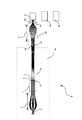
図1は、クリティカルな微小寸法測定装置1の光学系の構成を示す。クリティカルな微小寸法測定装置1は、ケーラー照明に基づく本発明によるフィールドと瞳の均質化システムを備えている。本実施形態では、ガス放電ランプが光源2として用意されている。ガス放電ランプにより放射される光は、集光器3により集められる。光源2は、集光器3の焦点に位置し、無限遠に発光プラズマ(luminous plasma)の像を結ぶ。照明のためのガス放電ランプのスペクトルのスペクトル成分を通過させるスペクトル性フィルタシステム4が集光器3の後のビームの進路に配置される。フィルタシステム4の後には第1のマイクロレンズアレイ配列5が配置され、その後には正の屈折力を持つ第1の補助的な光学素子6が配置される。図2は、第1の照明の均質化部を含む、図1の詳細部Aの拡大したものを示す。これについては、以下でより詳細に述べる。
FIG. 1 shows the configuration of the optical system of the critical dimension measuring apparatus 1. The critical dimension measuring device 1 comprises a field and pupil homogenization system according to the invention based on Koehler illumination. In the present embodiment, a gas discharge lamp is provided as the light source 2. The light emitted by the gas discharge lamp is collected by a light collector 3. The light source 2 is located at the focal point of the light collector 3 and forms an image of a luminous plasma at infinity. A spectral filter system 4 that passes the spectral components of the spectrum of the gas discharge lamp for illumination is arranged in the beam path after the collector 3. After the filter system 4, a first
第1のマイクロレンズアレイ配列5は、屈折あるいは回折のマイクロレンズアレイ、または2以上のアレイの組合せであったもよい。個々のマイクロレンズは、例えば六角形あるいは正方形の輪郭を持つものであってもよい。マイクロレンズは、収束レンズあるいは発散レンズとしてもよい。また、2つのマイクロレンズアレイを配置し、各マイクロレンズアレイは互いに交差する方向(crossed orientation)に配置された円柱状のマイクロレンズから構成することが考えられる。図示の便宜上第1のマイクロレンズアレイ配列5の3つのマイクロレンズI、II、IIIのみが描かれている。ここでは3つのマイクロレンズに減少させて描かれているが、実際には多数のマイクロレンズからマイクロレンズアレイは構成される。マイクロレンズアレイとして第1のマイクロレンズアレイ配列5が使われ、個々のマイクロレンズは全く同一のものである。
The first
各マイクロレンズI、II、IIIは、ビーム角8を有する円錐形の光線束7を生成する。以下でビーム角8は、広がり角ないし発散角(divergence angle)あるいは単に発散度(divergence)と称される。この発散度は、各マイクロレンズI、II、IIIから発せられる光線束7がコンデンサ11のコンデンサ瞳面10内のコンデンサ瞳9を完全に照明するように選ばれる。コンデンサ瞳9を持つコンデンサ瞳面10の位置は、図1の詳細部Bの拡大である図3に示される。これから明らかなようにここで用いられるコンデンサ11の実施形態では、コンデンサ瞳面10は第1のコンデンサレンズ12と第2のコンデンサレンズ13との間に置かれる。図2と図3の説明の目的では、第1のマイクロレンズアレイ配列5のマイクロレンズI、II、IIIから進行する例として描かれる光線には、同様にI、II、IIIの符号が付けられている。
Each microlens I, II, III produces a conical light bundle 7 having a beam angle 8. In the following, the beam angle 8 is referred to as the divergence angle or divergence angle or simply the divergence. This divergence is chosen such that the light beam 7 emitted from each microlens I, II, III completely illuminates the
光線束7の発散度は、個々のマイクロレンズI、II、IIIの屈折力(refractive power)により決定される。第1のマイクロレンズアレイ配列5のコンデンサ側の焦点面14からコンデンサ瞳9までの距離に広がり角8の半分の正接を掛けたものがコンデンサ瞳9の半径15以上になるように、個々のマイクロレンズの屈折力、すなわち発散度が選ばれる。
発 The divergence of the light beam 7 is determined by the refractive power of the individual microlenses I, II, III. The individual micro-lenses are arranged such that the distance from the
第1の補助的な光学素子6が無いと、個々のマイクロレンズI、II、IIIから進行する個々の収束あるいは発散する光線束(複数)7が同じビーム角8(すなわち同一の発散度)を示すが、異なる横方向のずれ(lateral offsets)を持ってコンデンサ瞳面10に到達するだろう。このずれのために光線束(複数)7の成分(複数)がコンデンサ瞳9の外側に入射してしまうだろう。この結果、光の強度の損失と、コンデンサ瞳9のエッジでの明るさの低下を生じてしまうだろう。
Without the first auxiliary optical element 6, the individual converging or diverging ray bundles 7 traveling from the individual microlenses I, II, III have the same beam angle 8 (ie the same divergence). As shown, the
これを防止するためにマイクロレンズI、II、IIIから進行する全ての光線束(複数)7が、第1の補助的な光学素子6によってコンデンサ瞳9に向けられる。この目的のために正の屈折力を持つ第1の補助的な光学素子6が使われる。第1の補助的な光学素子6の焦点距離は、第1の補助的な光学素子6とコンデンサ瞳9との間の距離に実質上等しい。その結果、個々のマイクロレンズI、II、IIIから進行する光線束(複数)7の中心光線(center rays)は、第1の補助的な光学素子6の前では平行に走るが、第1の補助的な光学素子6の後ではコンデンサ瞳9の中心に収束して向かうようになる。言い換えれば、コンデンサ瞳面10内で照明される領域は、コンデンサ瞳それ自身よりいくらか大きくなる。しかし図示の明瞭さのために図3ではコンデンサ瞳9が溢れ出るようにせずに単に一杯になるように示してある。溢れ出るようにするには十分に大きな数の光線を描く必要があるからである。
In order to prevent this, all light fluxes 7 traveling from the microlenses I, II, III are directed to the
多数のマイクロレンズによって強度が平均化され、コンデンサ瞳9における強度分布の均質化がなされる。ガス放電ランプ(すなわち光源2)の発光プラズマの中間像(intermediate images)が第1のマイクロレンズアレイ配列5の個々のマイクロレンズのコンデンサ側の焦点面14(すなわち焦点面)付近に作られる。この中間像の数はマイクロレンズI、II、IIIの数に対応する。
(4) The intensity is averaged by a number of microlenses, and the intensity distribution in the
これらの中間像は、正の屈折力を持つ第2の補助的な光学素子16と第2のマイクロレンズアレイ配列17とによって、コンデンサ瞳9すなわちコンデンサ瞳面10内に多数そして互いにずれたように結像される。実際には多くのマイクロレンズが存在するが、簡略化のために第2のマイクロレンズアレイ配列17の3つのマイクロレンズのみが図1および図3では概略的に描かれている。
These intermediate images are in large numbers and offset from one another in the
第2の補助的な光学素子16の効果は、中間像(焦点面14に位置する)から進行して発散する光線束(複数)の中心光線を整列(align the center rays)することにある。第2の補助的な光学素子16の前では、これら個々の光線束の中心光線は、発散的に広がり、第2の補助的な光学素子16によって全体のシステムの光軸18(図2および図3に示す)に対して平行にされる。中間像から進行する各光線束が第2のマイクロレンズアレイ配列17の各マイクロレンズに当るように、第2のマイクロレンズアレイ配列17が配置される。
The effect of the second auxiliary
第2のマイクロレンズアレイ配列17の個々のマイクロレンズの発散度は、試料19上の均質照明フィールドの大きさを決定する。図によれば、コンデンサ瞳面10に到達する個々の光線束に対する小さなビーム角度の場合は、特徴部20が測定される試料19上の小さな均質照明フィールドとなることを意味する。同じようにコンデンサ瞳面10に到達する個々の光線束に対する大きなビーム角度(すなわち大きな発散度)の場合は、測定される試料19上の大きな均質照明フィールドとなるが、小さなフィールドの場合より強度は低くなる。照明される目標のフィールドの大きさは、第2のマイクロレンズアレイ配列17のマイクロレンズの焦点距離の適切な選択により決定される。第2の補助的な光学素子16と第2のマイクロレンズアレイ配列17とにより達せられる第2の多数の結像の動作によって光の強度のフィールドにおける均質化がなされる。これにより図4に示すコンデンサ瞳9における強度分布が得られる。先に述べたようにコンデンサ瞳9はわずかに溢れ出ている。
The divergence of the individual microlenses of the second
第2のマイクロレンズアレイ配列17の発散度とコンデンサ11の焦点距離とが、このように試料19の照明フィールドの大きさを決定する。第2のマイクロレンズアレイ配列17の発散度、すなわち第2のマイクロレンズアレイ配列17のマイクロレンズの発散度は、目的の照明フィールドが若干オーバ(溢れて)照明されるように選ばれるのが望ましい。
The divergence of the
図1に描くように、試料19は、透明な支持層ないし基体(substrate)であって、その表面の右側に示すように検査される特徴部20が配されている。この試料は、例えば半導体製造のマスクである。光学的な検査が透過光により実行される。検査される特徴部(features)20は焦点に位置する。画像光学システム21は、例えばカメラのような画像取得(撮像)装置22に試料19の特徴部を結像する。画像取得(撮像)装置22により取得された画像は、画像評価装置23に送られ、画像評価装置23は、画像から特徴部20のクリティカル微小寸法を決定する。画像評価装置23は、例えば関連のソフトウェアを備えた計算機を含むものである。
試 料 As depicted in FIG. 1, sample 19 is a transparent support or substrate with
1 微小寸法測定装置
2 光源
3 集光器
4 フィルタシステム
5 第1のマイクロレンズアレイ配列(MLA)
6 第1の補助的な光学素子
7 光線束
8 ビーム角=広がり角
9 コンデンサ瞳
10 コンデンサ瞳面
11 コンデンサ
12 第1のコンデンサレンズ
13 第2のコンデンサレンズ
14 第1のMLAのコンデンサ側の焦点面
15 コンデンサ瞳の半径
16 第2の補助的な光学素子
17 第2のマイクロレンズアレイ配列(MLA)
18 光軸
19 試料
20 特徴部
21 画像光学システム
22 画像取得(撮像)装置
23 画像評価装置
I、II、III マイクロレンズと関連の光線
DESCRIPTION OF SYMBOLS 1 Micro dimension measuring apparatus 2 Light source 3 Condenser 4
Reference Signs List 6 First auxiliary optical element 7 Beam bundle 8 Beam angle = spread
Claims (10)
前記ビーム成形光学系(3)と、前記コンデンサ(11)との間に順に、
a) コンデンサの瞳(9)を満たすような発散性の光線束(7)を夫々生成する各マイクロレンズ(I、II、III)からなる第1のマイクロレンズアレイ配列(5)、
b) 正の屈折力を持つ第1の補助的な光学素子(6)であって、その焦点面に該コンデンサの瞳(9)が配置されるもの、
c) 正の屈折力を持つ第2の補助的な光学素子(16)、
d) 第2のマイクロレンズアレイ配列(17)、
を配置することを特徴とする微小寸法測定装置。 A light source (2), a beam shaping optical system (3), and a condenser (11);
In order between the beam shaping optical system (3) and the condenser (11),
a) a first microlens array arrangement (5) consisting of microlenses (I, II, III) each producing a divergent ray bundle (7) to fill the pupil (9) of the condenser;
b) a first auxiliary optical element (6) having a positive refractive power, the pupil (9) of the condenser being arranged at the focal plane;
c) a second auxiliary optical element (16) having a positive refractive power,
d) a second microlens array arrangement (17),
A micro-size measuring device characterized by disposing.
2. The micro-dimension measuring device according to claim 1, wherein the second micro-lens array arrangement is configured as a micro honeycomb-shaped capacitor.
Applications Claiming Priority (1)
| Application Number | Priority Date | Filing Date | Title |
|---|---|---|---|
| DE10245473A DE10245473A1 (en) | 2002-09-28 | 2002-09-28 | Linewidths meter |
Publications (2)
| Publication Number | Publication Date |
|---|---|
| JP2004117365A true JP2004117365A (en) | 2004-04-15 |
| JP2004117365A5 JP2004117365A5 (en) | 2006-09-28 |
Family
ID=31969709
Family Applications (1)
| Application Number | Title | Priority Date | Filing Date |
|---|---|---|---|
| JP2003338380A Pending JP2004117365A (en) | 2002-09-28 | 2003-09-29 | Microscopic dimension measuring apparatus |
Country Status (4)
| Country | Link |
|---|---|
| US (1) | US6943901B2 (en) |
| EP (1) | EP1403676B1 (en) |
| JP (1) | JP2004117365A (en) |
| DE (2) | DE10245473A1 (en) |
Families Citing this family (1)
| Publication number | Priority date | Publication date | Assignee | Title |
|---|---|---|---|---|
| CN113251949B (en) * | 2021-06-18 | 2021-11-30 | 三代光学科技(天津)有限公司 | Method for generating single-point optical measurement path of micro-lens array surface shape |
Family Cites Families (11)
| Publication number | Priority date | Publication date | Assignee | Title |
|---|---|---|---|---|
| US5359440A (en) * | 1989-10-23 | 1994-10-25 | Sharp Kabushiki Kaisha | Image display apparatus with microlens plate having mutually fused together lenses resulting in hexagonal shaped microlenses |
| JPH0560982A (en) * | 1991-08-30 | 1993-03-12 | Nikon Corp | Kohler illumination optical system |
| ES2182907T3 (en) * | 1994-06-14 | 2003-03-16 | Visionix Ltd | APPARATUS TO CARTOGRAPH OPTICAL ELEMENTS. |
| US5473408A (en) * | 1994-07-01 | 1995-12-05 | Anvik Corporation | High-efficiency, energy-recycling exposure system |
| TW374864B (en) * | 1994-10-28 | 1999-11-21 | Toshiba Corp | Projecting type displaying device and photo-modulating elements array used therein |
| JPH1164787A (en) * | 1997-08-21 | 1999-03-05 | Seiko Epson Corp | Projection type display device |
| JPH11174372A (en) * | 1997-12-11 | 1999-07-02 | Victor Co Of Japan Ltd | Illumination device for projection device and projection device |
| DE10062579A1 (en) * | 1999-12-15 | 2001-06-21 | Nikon Corp | Optical integrator of wave front subdividing type used for photolithographic illuminating device comprises micro-optical elements arranged two-dimensionally to form light sources by subdividing wave front of falling light beam |
| DE10031719A1 (en) * | 2000-06-29 | 2002-01-10 | Leica Microsystems | Illumination device and coordinate measuring device with an illumination device |
| JP2002023061A (en) * | 2000-07-11 | 2002-01-23 | Nikon Corp | Device and method for illuminating dark field of microscope |
| US6731383B2 (en) * | 2000-09-12 | 2004-05-04 | August Technology Corp. | Confocal 3D inspection system and process |
-
2002
- 2002-09-28 DE DE10245473A patent/DE10245473A1/en not_active Withdrawn
-
2003
- 2003-09-24 DE DE50303167T patent/DE50303167D1/en not_active Expired - Lifetime
- 2003-09-24 EP EP03021531A patent/EP1403676B1/en not_active Expired - Fee Related
- 2003-09-26 US US10/672,048 patent/US6943901B2/en not_active Expired - Fee Related
- 2003-09-29 JP JP2003338380A patent/JP2004117365A/en active Pending
Also Published As
| Publication number | Publication date |
|---|---|
| EP1403676A1 (en) | 2004-03-31 |
| DE10245473A1 (en) | 2004-04-08 |
| DE50303167D1 (en) | 2006-06-08 |
| US6943901B2 (en) | 2005-09-13 |
| US20040070821A1 (en) | 2004-04-15 |
| EP1403676B1 (en) | 2006-05-03 |
Similar Documents
| Publication | Publication Date | Title |
|---|---|---|
| TWI382202B (en) | Catadioptric optical system for scatterometry | |
| JP2007527545A (en) | Inspection system using small catadioptric objective | |
| JP2008275612A (en) | Device equipped with high resolution measurement structure on substrate for manufacturing semiconductor, and use of aperture in measuring device | |
| TWI569002B (en) | Metrology tool, catadioptric optical system, and metrology method | |
| JP6370626B2 (en) | Illumination optical system, illumination device, and illumination optical element | |
| TWI803714B (en) | Light source apparatus, illumination apparatus, exposure apparatus, and method for manufacturing object | |
| JP6546172B2 (en) | Reflective optical element, in particular a measuring arrangement for measuring the optical properties of microlithography | |
| TWI647448B (en) | Lens array-based illumination for wafer inspection | |
| US7001055B1 (en) | Uniform pupil illumination for optical inspection systems | |
| JP3303595B2 (en) | Illumination device and observation device using the same | |
| TWI809281B (en) | Method for determining a production aerial image of an object to be measured | |
| JP5261095B2 (en) | Illumination optical system for image sensor inspection | |
| JP2004117365A (en) | Microscopic dimension measuring apparatus | |
| JP2008182244A (en) | Optical integrator for illumination system of microlithographic projection exposure apparatus | |
| CN104122757B (en) | prism optical system, illumination optical system, exposure apparatus, and device manufacturing method | |
| KR101999553B1 (en) | Illumination optical device, exposure apparatus, and method of manufacturing article | |
| JP2000019012A (en) | Lighting system brightness distribution measuring device | |
| US20230418081A1 (en) | Light source system and method | |
| CN101113937A (en) | Compound eye lens simple detecting method | |
| JP2008064759A (en) | Device and method for optically detecting surface error of substrate | |
| TWI547768B (en) | Prism optical system, illumination optical system, exposure apparatus, and device manufacturing method | |
| JP4500919B2 (en) | Microscope device and object observation method | |
| TW202336530A (en) | Metrology system for examining objects with euv measurement light | |
| JP2013239709A (en) | Optical assembly for euv lithography | |
| JP2007132975A (en) | Light source device |
Legal Events
| Date | Code | Title | Description |
|---|---|---|---|
| A521 | Written amendment |
Free format text: JAPANESE INTERMEDIATE CODE: A523 Effective date: 20060809 |
|
| A621 | Written request for application examination |
Free format text: JAPANESE INTERMEDIATE CODE: A621 Effective date: 20060809 |
|
| A977 | Report on retrieval |
Free format text: JAPANESE INTERMEDIATE CODE: A971007 Effective date: 20090109 |
|
| A131 | Notification of reasons for refusal |
Free format text: JAPANESE INTERMEDIATE CODE: A131 Effective date: 20090224 |
|
| A02 | Decision of refusal |
Free format text: JAPANESE INTERMEDIATE CODE: A02 Effective date: 20090721 |