EP1403676B1 - Apparatus for measuring structure widths - Google Patents
Apparatus for measuring structure widths Download PDFInfo
- Publication number
- EP1403676B1 EP1403676B1 EP03021531A EP03021531A EP1403676B1 EP 1403676 B1 EP1403676 B1 EP 1403676B1 EP 03021531 A EP03021531 A EP 03021531A EP 03021531 A EP03021531 A EP 03021531A EP 1403676 B1 EP1403676 B1 EP 1403676B1
- Authority
- EP
- European Patent Office
- Prior art keywords
- microlens array
- array arrangement
- condenser
- measuring structure
- microlenses
- Prior art date
- Legal status (The legal status is an assumption and is not a legal conclusion. Google has not performed a legal analysis and makes no representation as to the accuracy of the status listed.)
- Expired - Fee Related
Links
Images

Classifications
-
- G—PHYSICS
- G01—MEASURING; TESTING
- G01B—MEASURING LENGTH, THICKNESS OR SIMILAR LINEAR DIMENSIONS; MEASURING ANGLES; MEASURING AREAS; MEASURING IRREGULARITIES OF SURFACES OR CONTOURS
- G01B11/00—Measuring arrangements characterised by the use of optical techniques
Definitions
- the invention relates to a structure width measuring device with a light source, a beam shaping optics, and a condenser.
- Texture width measuring devices are used in the production of critical dimension measuring devices (cd) to check the dimensional accuracy of structures on semiconductor chips according to the individual production steps and to control the quality of the production steps.
- critical dimension measuring devices cd
- the structural widths of the structures to be measured are becoming smaller and smaller. Accordingly, the requirements for the specifications of measuring and inspection systems, e.g. the requirements for the measuring accuracy and the repeatability of the measurement results.
- Optical probing methods and corresponding optical measuring devices are preferred in production, although the pattern widths of the structures to be measured are already smaller than the optical wavelength used for measurement or inspection. This is because the optical measuring devices are much easier to use than the non-optical ones. At the same time, however, the demands on the optical measuring devices, in particular with respect to the resolution and the separation of neighboring structures. In this case, the quality of the illumination of the structures to be examined plays a decisive role. In order to be able to measure structural widths, edge profiles and similar critical quantities reproducibly by optical means, the measuring fields, ie the structures detected during the measurement and their surroundings, must be illuminated extremely homogeneously for Fourier optical reasons.
- gas discharge lamps are used as light sources and the objects to be examined are illuminated in the manner of classic Köhler lighting.
- the known gas discharge lamps have unfavorable for the feature width measurement, i. asymmetric, near and far distributions of light intensity.
- Köhler illumination these field distributions result in uneven illumination of the optical measuring field and the pupil.
- the pupil is the objective pupil in incident-light illumination and the condenser pupil in transmitted-light illumination.
- the uneven illumination and in particular an oblique illumination has the consequence that the measured structure widths are dependent on the position and the orientation of the structure to be examined in the optical measuring field. This has the disadvantage that the high demands of the users on the reproducibility and independence of the measurement results from the measurement position and the orientation of the structure can not be met.
- DE 100 62 579 A1 describes a photolithography exposure device with an illumination device which has an optical integrator according to the principle of wavefront subdivision.
- the laser originating device passes through a beam expander, a first microlens array, a positive lens and the optical integrator, which is composed of two microlens arrays.
- a second positive lens serves as a condenser.
- the US 2002/0001090 A1 describes a coordinate measuring machine, which determines the position of structures on an object and thus also allows a structured-beam measurement.
- the light of a light source is coupled into a fiber bundle at the other end coupled again and directed to a single-stage Homogenfal mecanicsoptik consisting of a In this way, a one-stage homogenization of the illumination is achieved.
- lasers are used as light sources. This has the disadvantage that the radiation emitted by the laser is almost completely coherent. This high degree of coherence leads to self-interference of the radiation field. These are noticeable for example by laser light granulation in the measuring field and also influence the structure width measurement negatively, so that a high reproducibility and independence of the measurement results from the measuring position and the orientation of the structure is not possible.
- a laser can be arranged as the light source and a beam expansion optics can be arranged as beam shaping optics.
- the light source may be formed as a gas discharge lamp and the beam shaping optics as a collector.
- a spectrally effective filter system is provided, which only transmits the spectral component of the light source spectrum required for the respective measurement.
- the spectrally effective filter system is then arranged at the output of the collector.
- the microlens array arrangement may, for example, comprise a multiplicity of identical, hexagonal, honeycomb or square microlenses.
- the microlens array arrangement may comprise two microlens cylindrical microlens arrays each having a plurality of like cylindrical microlenses, the two microlens arrays being cylindrical in relation to the cylinder axes Microlenses are arranged crossed.
- the microlens array arrangement may also be designed as a micro-cell condenser.
- the invention is based on the consideration that a reliable structure width measurement is only possible if there is a uniform field illumination on the object to be examined and an at least rotationally symmetrical intensity distribution in the pupil of the condenser. Both conditions are a necessary prerequisite for optical structure width measurement with high accuracy. This is due to the fact that any form of oblique illumination leads to different measurement results at the left edge and the right edge of a structure, so that the difference formation, ie the actual structure width determination, always has an error. Because of these requirements, ie a uniform field illumination and an at least rotationally symmetrical intensity distribution in the pupil, it is possible to carry out reproducible measurements of the width of microstructures and submicrostructures in the measurement field almost independently of the position and orientation of the structure to be investigated.
- the near and far field distributions of gas discharge lamps which are unfavorable for the structural width measurements, or the intensity differences due to laser light granulation in the measuring field must be homogenized in an analogous manner with illumination by means of a laser.
- the structure width measuring device has a two-stage homogenization in the illumination, so that illumination according to the Köhler principle is present, which has a homogeneous field illumination with simultaneous rotation-symmetrical intensity distribution in the pupil. Since the respective edge of a structure to be measured is positioned in the measurement field for the structure width measurement, the rotationally symmetrical intensity distribution in the pupil of the condenser ensures that both falling and rising edges, for example the left and the right edge of a structure, can be measured with the same intensity and illumination conditions. thats why With the present structure width measuring device for the first time a measurement of structure widths possible, which can be made independently of the position of the structure to be examined in the measuring field and independent of the orientation of the structure to be examined in the measuring field.
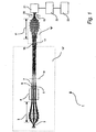
- FIG. 1 shows the schematic optical structure of a structure width measuring device 1 with a field and pupil homogenization according to the invention on the basis of Köhler illumination.
- a gas discharge lamp is arranged in the present embodiment.
- the light emitted from the gas discharge lamp is collected by a collector 3.
- the light source 2 is in the focus of the collector 3 and therefore reflects the luminous plasma after ⁇ .
- a spectrally effective filter system 4 is arranged after the collector 3, which filters out the intended for lighting spectral component of the lamp spectrum of the gas discharge lamp.
- a first microlens array arrangement 5 and then a first auxiliary optical element 6 with a positive refractive power is arranged.
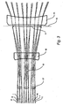
- FIG. 2 shows a detail enlargement "A" from FIG. 1 with this first homogenization stage of the illumination, which will be described in more detail below.
- the first microlens array arrangement 5 can be a refractive or diffractive microlens array or even a combination of two or more such arrays.
- the individual microlenses may have, for example, a hexagonal or a square contour.
- the microlenses can each be designed as collecting or dissipating lenses. It is also conceivable to arrange two microlens arrays each with cylindrical microlenses in a crossed orientation to each other. For reasons of clarity of the drawing, only three microlenses I, II and III are shown by the first microlens array arrangement 5. Thus, this is only a schematic reduction to three microlenses, while the actually arranged microlens array has a plurality of microlenses. As with known microlens arrays, the individual microlenses are the same even in the case of the first microlens array arrangement 5 used here.
- Each microlens I, II and III produces a cone-shaped beam 7 with an opening angle 8, which is referred to below as the divergence angle or as a short divergence.
- This divergence is chosen such that the beam 7 emanating from each microlens I, II and III completely illuminates the condenser pupil 9 in the condenser pupil plane 10 of the condenser 11.
- FIG. 3 shows an enlarged detail "B" of FIG .
- the condenser pupil plane 10 lies between the first condenser lens 12 and the second condenser lens 13.
- FIGS. 2 and 3 the rays drawn by way of example from the microlenses I, II and III of the first microlens array arrangement 5 are likewise denoted by I, II and III.
- the divergence of the beam 7 is determined by the refractive power of the individual microlenses I, II and III.
- the refractive power of the individual microlenses and thus the divergence is chosen so that the distance from the condenser-side focal plane 14 of the first microlens array array 5 to the Condenser pupil 9 multiplied by the tangent of the half divergence angle 8 ⁇ the radius 13 of the condenser pupil 9 is.
- the individual convergent or divergent beams 7 emanating from the individual microlenses I, II and III would all have the same opening angle 8, ie the same divergence, but with different lateral offset in the condenser pupil plane 10 arrive. This offset would cause portions of the radiation beams 7 to impinge outside the Kondersor pupil 9. This would lead to a loss of light intensity and a decrease in brightness at the edge of the Kondersor pupil 9.
- all beams 7 emanating from the microlenses I, II and III are aligned with the condenser pupil 9 by means of the first optical auxiliary element 6.
- a first auxiliary optical element 6 with positive refractive power is used.
- the focal length of the first auxiliary optical element 6 is substantially equal to the distance of the first auxiliary optical element 6 from the condenser pupil 9. This causes the center rays of the emanating from the individual microlenses I, II and III beams 7, the front of the first optical Auxiliary element 6 are still parallel, now after the first optical auxiliary element 6 are convergently directed into the center of the condenser pupil 9.
- the condenser pupil 9 is slightly over-operated.
- Fig. 3 shows, for reasons of clarity, the condenser pupil 9, however, only filled, not over-served, as this much more rays would have to be displayed.
- the plurality of microlenses leads to an intensity averaging and thus to a homogenization of the intensity distribution in the condenser pupil 9.
- the individual microlenses of the first microlens array arrangement 5 intermediate images of the luminous plasma are formed the gas discharge lamp, so the Light source 2.
- the number of these intermediate images corresponds to the number of microlenses I, II and III.
- the second auxiliary optical element 16 causes the center rays of the divergent beams emanating from the individual intermediate images (located in the focal plane 14) to be aligned.
- the center rays of these individual ray bundles extend divergently and are aligned by the second auxiliary optical element 16 parallel to the optical axis 18 (shown in FIGS. 2 and 3 ) of the overall system.
- the second microlens array arrangement 17 is aligned such that in each case a beam emanating from an intermediate image strikes a microlens of the second microlens array arrangement 17.
- the divergence of the individual microlenses of the second microlens array arrangement 17 determines how large the homogenous field illuminated on the object 19 is. This clearly indicates that a small opening angle of the individual beams impinging in the condenser pupil plane 10 causes a small, homogeneously illuminated field on the object 19 whose structures 20 are to be measured. Similarly, a large aperture angle, ie a large divergence, causes the individual beams incident in the condenser pupil plane 10 to emit a large, homogeneously illuminated field on the object 19 to be measured, albeit at a lower intensity than in the small field.
- the size of the illuminated object field is determined.
- the with the second optical sub-array 16 and the second micro-lens array array 17 scored second multiple image causes the field homogenization of the light intensity.
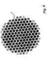
- the intensity distribution in the condenser pupil 9 shown in FIG. 4 is obtained .
- the condenser pupil 9 is slightly over-operated.
- the divergence of the second microlens array 17 and the focal length of the condenser 11 determine the size of the illuminated field on the object 19.
- the divergence of the second microlens array 17, i. the microlenses of this second microlens array arrangement 17, chosen so that the object field to be illuminated is slightly outshone.
- the object 19 is a transparent substrate on whose surface shown on the right the structures 20 to be examined are applied.
- this object may be a mask for semiconductor fabrication.
- the optical examination is therefore carried out in transmitted light.
- the structures 20 to be examined are in focus.
- An imaging optical system 21 images the structures of the object 19 onto an image recording device 22, which may be, for example, a camera.
- the recorded images of the image recording device 22 are transmitted to an image evaluation device 23 which determines the structure widths of the structures 20 from the images.
- the image evaluation device 23 may comprise, for example, a computer with the associated software.
Landscapes
- Physics & Mathematics (AREA)
- General Physics & Mathematics (AREA)
- Length Measuring Devices By Optical Means (AREA)
- Photometry And Measurement Of Optical Pulse Characteristics (AREA)
- Microscoopes, Condenser (AREA)
Description
Die Erfindung betrifft ein Strukturbreiten-Messgerät mit einer Lichtquelle, einer Strahlformungsoptik, und einem Kondensor.The invention relates to a structure width measuring device with a light source, a beam shaping optics, and a condenser.
Strukturbreiten-Messgeräte werden in der Produktion von Halbleitem zum Messen von Strukturbreiten (englisch: critical dimension = cd) eingesetzt, um die Maßhaltigkeit von Strukturen auf Halbleiter-Chips nach den einzelnen Produktionsschritten zu überprüfen und die Qualität der Produktionsschritte zu steuern. Bei ständig steigenden Packungsdichten auf den Halbleiter-Chips werden zugleich die Strukturbreiten der zu vermessenden Strukturen immer kleiner. Entsprechend steigen die Anforderungen an die Spezifikationen von Mess- und Inspektionssystemen, z.B. die Anforderungen an die Messgenauigkeit und die Wiederholbarkeit der Messergebnisse.Texture width measuring devices are used in the production of critical dimension measuring devices (cd) to check the dimensional accuracy of structures on semiconductor chips according to the individual production steps and to control the quality of the production steps. At constantly increasing packing densities on the semiconductor chips, the structural widths of the structures to be measured are becoming smaller and smaller. Accordingly, the requirements for the specifications of measuring and inspection systems, e.g. the requirements for the measuring accuracy and the repeatability of the measurement results.
Optische Antastverfahren und entsprechende optische Mess-Vorrichtungen werden in der Produktion bevorzugt, obwohl die Strukturbreiten der zu vermessenden Strukturen schon kleiner als die zum Messen bzw. zur Inspektion verwendete optische Wellenlänge sind. Dies liegt daran, dass die optischen Mess-Vorrichtungen wesentlich leichter zu benutzen sind als die nicht-optischen. Gleichzeitig steigen aber die Anforderungen an die optischen Mess-Vorrichtungen, insbesondere bezüglich des Auflösungsvermögens und der Trennung von benachbarten Strukturen. Eine entscheidende Rolle spielt hierbei die Güte der Beleuchtung der zu untersuchenden Strukturen. Um Strukturbreiten, Kantenprofile und ähnliche kritische Größen mit optischen Mitteln reproduzierbar vermessen zu können, müssen aus Fourier-optischen Gründen die Messfelder, also die bei der Messung erfassten Strukturen und deren Umgebung, extrem homogen ausgeleuchtet werden.Optical probing methods and corresponding optical measuring devices are preferred in production, although the pattern widths of the structures to be measured are already smaller than the optical wavelength used for measurement or inspection. This is because the optical measuring devices are much easier to use than the non-optical ones. At the same time, however, the demands on the optical measuring devices, in particular with respect to the resolution and the separation of neighboring structures. In this case, the quality of the illumination of the structures to be examined plays a decisive role. In order to be able to measure structural widths, edge profiles and similar critical quantities reproducibly by optical means, the measuring fields, ie the structures detected during the measurement and their surroundings, must be illuminated extremely homogeneously for Fourier optical reasons.
Dazu werden in den bekannten Strukturbreiten-Messgeräten unterschiedliche Arten von Beleuchtungseinrichtungen eingesetzt. So werden in einer Art der Beleuchtungseinrichtungen als Lichtquellen Gas-Entladungslampen eingesetzt und die zu untersuchenden Objekte nach Art der klassischen Köhler-Beleuchtung ausgeleuchtet. Die bekannten Gas-Entladungslampen weisen für die Strukturbreiten-Messung ungünstige, d.h. asymmetrische, Nah-und Fernverteilungen der Lichtintensität auf. Diese Feldverteilungen führen bei einer Köhler-Beleuchtung zu einer ungleichmäßigen Ausleuchtung des optischen Messfelds und der Pupille. Als Pupille wird dabei in einer Auflicht-Beleuchtung die Objektiv-Pupille und in einer Durchlicht-Beleuchtung die Kondensor-Pupille bezeichnet. Die ungleichmäßige Ausleuchtung und insbesondere eine schräge Beleuchtung hat zur Folge, dass die gemessenen Strukturbreiten von der Position und der Orientierung der zu untersuchenden Struktur im optischen Messfeld abhängig sind. Dies hat den Nachteil, dass die hohen Anforderungen der Anwender an die Reproduzierbarkeit und Unabhängigkeit der Messergebnisse von der Messposition und der Orientierung der Struktur nicht erfüllt werden können.For this purpose, different types of lighting devices are used in the known structure width measuring devices. Thus, in one type of lighting devices, gas discharge lamps are used as light sources and the objects to be examined are illuminated in the manner of classic Köhler lighting. The known gas discharge lamps have unfavorable for the feature width measurement, i. asymmetric, near and far distributions of light intensity. With Köhler illumination, these field distributions result in uneven illumination of the optical measuring field and the pupil. The pupil is the objective pupil in incident-light illumination and the condenser pupil in transmitted-light illumination. The uneven illumination and in particular an oblique illumination has the consequence that the measured structure widths are dependent on the position and the orientation of the structure to be examined in the optical measuring field. This has the disadvantage that the high demands of the users on the reproducibility and independence of the measurement results from the measurement position and the orientation of the structure can not be met.
Die DE 100 62 579 A1 beschreibt eine Photollthographie-Belichtungseinrichtung mit einer Beleuchtungseinrichtung, die einen optischen Integrierer nach dem Prinzip der Wellenfrontunterteilung aufweist. Das von einer Laser ausgehende Ucht durchläuft einen Strahlaufweiter, eine erstes Mikrolinsen-Array, eine Positivlinse sowie den optischen Integrierer, der aus zwei Mikrolinsen-Arrays aufgebaut ist. Eine zweite Positivlinse dient als Kondensor. Mittels geeigneter Blenden wird ein für den Lithographie-Prozess geeignetes kleines Beieuehtungsfeid erzielt.DE 100 62 579 A1 describes a photolithography exposure device with an illumination device which has an optical integrator according to the principle of wavefront subdivision. The laser originating device passes through a beam expander, a first microlens array, a positive lens and the optical integrator, which is composed of two microlens arrays. A second positive lens serves as a condenser. By means of suitable apertures a suitable for the lithography process small Beieehtungsfeid is achieved.
Die US 2002/0001090 A1 beschreibt eine Koordinatenmessmaschine, welche die Position von Strukturen auf einem Objekt bestimmt und somit auch eine Strukturbreltenmessung erlaubt Das Licht einer Lichtquelle wird in ein Faserbündel eingekoppelt an dessen anderen Ende wieder ausgekoppelt und auf eine einstufige Homogenfalerungsoptik geleitet, die aus einem Mikrowabenkondensor und einem als Kondensor wirkenden Linsenglied besteht Auf diese Weise wird eine einstufige Homogenisierung der Beleuchtung erzielt.The US 2002/0001090 A1 describes a coordinate measuring machine, which determines the position of structures on an object and thus also allows a structured-beam measurement. The light of a light source is coupled into a fiber bundle at the other end coupled again and directed to a single-stage Homogenfalerungsoptik consisting of a In this way, a one-stage homogenization of the illumination is achieved.
In anderen Strukturbreiten-Messgeräten werden Laser als Lichtquellen eingesetzt. Dies hat den Nachteil, dass die von dem Laser emittierte Strahlung nahezu vollständig kohärent ist. Dieser hohe Kohärenzgrad führt zu Eigeninterferenzen des Strahlungsfeldes. Diese machen sich beispielsweise durch Laserlicht-Granulation im Messfeld bemerkbar und beeinflussen die Strukturbreiten-Messung ebenfalls negativ, so dass eine hohe Reproduzierbarkeit und Unabhängigkeit der Messergebnisse von der Messposition und der Orientierung der Struktur nicht möglich ist.In other structure-width measuring devices, lasers are used as light sources. This has the disadvantage that the radiation emitted by the laser is almost completely coherent. This high degree of coherence leads to self-interference of the radiation field. These are noticeable for example by laser light granulation in the measuring field and also influence the structure width measurement negatively, so that a high reproducibility and independence of the measurement results from the measuring position and the orientation of the structure is not possible.
Es ist daher Aufgabe der vorliegenden Erfindung, ein Strukturbreiten-Messgerät anzugeben, mit dem reproduzierbare, von der Messposition und der Orientierung der Struktur unabhängige Strukturbreiten-Messungen möglich sind.It is therefore an object of the present invention to provide a structure-width measuring device, with the reproducible, independent of the measurement position and the orientation of the structure structure width measurements are possible.
Diese Aufgabe wird gelöst durch ein Strukturbreiten-Messgerät gemäss Anspruch 1.This object is achieved by a structure width measuring device according to
Als Lichtquelle kann ein Laser und als Strahlformungsoptik eine Strahlaufweitungsoptik angeordnet sein. Alternativ kann die Lichtquelle als eine Gasentladungslampe und die Strahlformungsoptik als ein Kollektor ausgebildet sein. In diesem Fall ist es vorteilhaft, wenn zusätzlich ein spektral wirksames Filtersystem vorgesehen ist, welches nur den für die jeweilige Messung erforderlichen Spektralanteil des Lichtquellenspektrums durchlässt. In diesem Fall ist dann das spektral wirksame Filtersystem am Ausgang des Kollektors angeordnet.A laser can be arranged as the light source and a beam expansion optics can be arranged as beam shaping optics. Alternatively, the light source may be formed as a gas discharge lamp and the beam shaping optics as a collector. In this case, it is advantageous if, in addition, a spectrally effective filter system is provided, which only transmits the spectral component of the light source spectrum required for the respective measurement. In this case, the spectrally effective filter system is then arranged at the output of the collector.
Die Mikrolinsenarray-Anordnung kann beispielsweise eine Vielzahl von gleichen, sechseckigen, wabenförmigen oder quadratischen Mikrolinsen aufweisen. Alternativ kann die Mikrolinsenarray-Anordnung zwei Mikrolinsenarrays mit zylindrischen Mikrolinsen aufweisen, die jeweils eine Vielzahl von gleichen, zylindrischen Mikrolinsen aufweisen, wobei die beiden Mikrolinsenarrays in Bezug auf die Zylinderachsen der zylindrischen Mikrolinsen gekreuzt angeordnet sind. Die Mikrolinsenarray-Anordnung kann auch als ein Mikrowabenkondensor ausgebildet sein.The microlens array arrangement may, for example, comprise a multiplicity of identical, hexagonal, honeycomb or square microlenses. Alternatively, the microlens array arrangement may comprise two microlens cylindrical microlens arrays each having a plurality of like cylindrical microlenses, the two microlens arrays being cylindrical in relation to the cylinder axes Microlenses are arranged crossed. The microlens array arrangement may also be designed as a micro-cell condenser.
Der Erfindung liegt die Überlegung zugrunde, dass eine zuverlässige Strukturbreiten-Messung nur möglich ist, wenn eine gleichmäßige Feldausleuchtung auf dem zu untersuchenden Objekt und eine zumindest rotationssymmetrische Intensitätsverteilung in der Pupille des Kondensors vorliegen. Beide Bedingungen sind eine notwendige Voraussetzung für eine optische Strukturbreiten-Messung mit hoher Genauigkeit. Dies liegt daran, dass jegliche Form von schräger Beleuchtung zu unterschiedlichen Messergebnissen an der linken Kante und der rechten Kante einer Struktur führen, so dass die Differenzbildung, also die eigentliche Strukturbreiten-Bestimmung, stets mit einem Fehler behaftet ist. Aufgrund dieser Voraussetzungen, also einer gleichmäßigen Feldausleuchtung und einer zumindest rotationssymmetrischen Intensitätsverteilung in der Pupille, ist es möglich, nahezu unabhängig von der Position und der Orientierung der zu untersuchenden Struktur im Messfeld reproduzierbare Messungen der Breite von Mikro- und Submikrostrukturen durchzuführen. Will man also die aus dem Stand der Technik bekannten Nachteile der Beleuchtungsinhomogenitäten vermeiden, so müssen die für die Strukturbreitenmessungen ungünstigen Nah- und Femfeldverteilungen von Gasentladungslampen bzw. in analoger Weise bei einer Beleuchtung mittels eines Lasers die Intensitätsunterschiede durch Laserlichtgranulation im Messfeld homogenisiert werden.The invention is based on the consideration that a reliable structure width measurement is only possible if there is a uniform field illumination on the object to be examined and an at least rotationally symmetrical intensity distribution in the pupil of the condenser. Both conditions are a necessary prerequisite for optical structure width measurement with high accuracy. This is due to the fact that any form of oblique illumination leads to different measurement results at the left edge and the right edge of a structure, so that the difference formation, ie the actual structure width determination, always has an error. Because of these requirements, ie a uniform field illumination and an at least rotationally symmetrical intensity distribution in the pupil, it is possible to carry out reproducible measurements of the width of microstructures and submicrostructures in the measurement field almost independently of the position and orientation of the structure to be investigated. If, therefore, one wishes to avoid the drawbacks of the inhomogeneities known from the prior art, the near and far field distributions of gas discharge lamps, which are unfavorable for the structural width measurements, or the intensity differences due to laser light granulation in the measuring field must be homogenized in an analogous manner with illumination by means of a laser.
Dazu weist das erfindungsgemäße Strukturbreiten-Messgerät eine zweistufige Homogenisierung in der Beleuchtung auf, so dass eine Beleuchtung nach dem Köhler'schen Prinzip vorliegt, welche eine homogene Feldausleuchtung bei gleichzeitiger rotationssymmetrischer Intensitätsverteilung in der Pupille aufweist. Da für die Strukturbreiten-Messung die jeweils zu vermessende Kante einer Struktur im Messfeld positioniert wird, wird durch die rotationssymmetrische Intensitätsverteilung in der Pupille des Kondensors sichergestellt, dass sowohl bei fallenden als auch ansteigenden Kanten, also beispielsweise der linken und der rechten Kante einer Struktur, mit denselben Intensitäts- und Beleuchtungsverhältnissen gemessen werden kann. Daher ist mit dem vorliegenden Strukturbreiten-Messgerät erstmals eine Messung von Strukturbreiten möglich, die unabhängig von der Position der zu untersuchenden Struktur im Messfeld und unabhängig von der Orientierung der zu untersuchenden Struktur im Messfeld vorgenommen werden kann.For this purpose, the structure width measuring device according to the invention has a two-stage homogenization in the illumination, so that illumination according to the Köhler principle is present, which has a homogeneous field illumination with simultaneous rotation-symmetrical intensity distribution in the pupil. Since the respective edge of a structure to be measured is positioned in the measurement field for the structure width measurement, the rotationally symmetrical intensity distribution in the pupil of the condenser ensures that both falling and rising edges, for example the left and the right edge of a structure, can be measured with the same intensity and illumination conditions. thats why With the present structure width measuring device for the first time a measurement of structure widths possible, which can be made independently of the position of the structure to be examined in the measuring field and independent of the orientation of the structure to be examined in the measuring field.
Die Erfindung wird nachfolgend anhand der schematischen Zeichnung ausführlich beschrieben. Es zeigen:
- Fig. 1:
- ein Strukturbreiten-Messgerät mit einer Gasentladungslampe als Lichtquelle;
- Fig. 2 :
- eine Detailvergrößerung "A" aus der Fig. 1 mit der ersten Homogenisierungsstufe der Beleuchtung;
- Fig. 3 :
- eine weitere Detailvergrößerung "B" aus der Fig. 1 mit der zweiten Homogenisierungsstufe der Beleuchtung;
- Fig. 4 :
- Intensitätsverteilung in der Pupille.
- Fig. 1 :
- a structure width measuring device with a gas discharge lamp as a light source;
- Fig. 2 :
- a detail enlargement "A" of Figure 1 with the first homogenization stage of the illumination.
- 3 :
- a further detail enlargement "B" of Figure 1 with the second homogenization stage of lighting.
- 4 :
- Intensity distribution in the pupil.
Fig. 1 zeigt den schematischen optischen Aufbau eines Strukturbreiten-Messgerätes 1 mit einer erfindungsgemäßen Feld- und Pupillenhomogenisierung auf Basis einer Köhler'schen Beleuchtung. Als Lichtquelle 2 ist in der vorliegenden Ausführungsform eine Gasentladungslampe angeordnet. Das von der Gasentladungslampe emittierte Licht wird von einem Kollektor 3 gesammelt. Die Lichtquelle 2 steht im Fokus des Kollektors 3 und bildet daher das leuchtende Plasma nach ∞ ab. Im Strahlengang ist nach dem Kollektor 3 ein spektral wirksames Filtersystem 4 angeordnet, das den zur Beleuchtung bestimmten spektralen Anteil des Lampenspektrums der Gasentladungslampe herausfiltert. Nach dem Filtersystem 4 ist eine erste Mikrolinsenarray-Anordnung 5 und danach ein erstes optisches Hilfselement 6 mit positiver Brechkraft angeordnet. Fig. 2 zeigt eine Detailvergrößerung "A" aus der Fig. 1 mit dieser ersten Homogenisierungsstufe der Beleuchtung, die nachfolgend näher beschrieben wird. 1 shows the schematic optical structure of a structure width measuring
Bei der ersten Mikrolinsenarray-Anordnung 5 kann es sich um ein refraktives oder diffraktives Mikrolinsenarray oder auch um eine Kombination aus zwei oder mehreren solcher Arrays handeln. Dabei können die einzelnen Mikrolinsen beispielsweise eine sechseckige oder auch eine quadratische Kontur aufweisen. Die Mikrolinsen können jeweils als sammelnde oder zerstreuende Linsen ausgebildet sein. Es ist auch denkbar, zwei Mikrolinsenarrays mit jeweils zylindrischen Mikrolinsen in gekreuzter Orientierung zueinander anzuordnen. Aus Gründen der Anschaulichkeit der Zeichnung sind von der ersten Mikrolinsenarray-Anordnung 5 nur drei Mikrolinsen I, II und III dargestellt. Hierbei handelt es sich also lediglich um eine schematische Reduzierung auf drei Mikrolinsen, während das tatsächlich angeordnete Mikrolinsenarray eine Vielzahl von Mikrolinsen aufweist. Wie bei bekannten Mikrolinsenarrays sind auch bei der hier verwendeten ersten Mikrolinsenarray-Anordnung 5 die einzelnen Mikrolinsen gleich.The first
Jede Mikrolinse I, II und III erzeugt ein kegelförmiges Strahlenbündel 7 mit einem Öffnungswinkel 8, der nachfolgend als Divergenzwinkel bzw. als kurz als Divergenz bezeichnet wird. Diese Divergenz wird so gewählt, dass das von jeder Mikrolinse I, II und III ausgehende Strahlenbündel 7 die Kondensor-Pupille 9 in der Kondensor-Pupillenebene 10 des Kondensors 11 vollständig ausleuchtet. Die Lage der Kondensor-Pupillenebene 10 mit der Kondensor-Pupille 9 ist in Fig. 3 dargestellt, welche eine Detailvergrößerung "B" der Fig. 1 zeigt. Daraus geht hervor, dass bei der hier verwendeten Ausführungsform des Kondensors 11 die Kondensor-Pupillenebene 10 zwischen der ersten Kondensorlinse 12 und der zweiten Kondensorlinse 13 liegt. Zur Veranschaulichung sind in den Fig. 2 und Fig. 3 die von den Mikrolinsen I, II und III der ersten Mikrolinsenarray-Anordnung 5 ausgehenden, beispielhaft gezeichneten Strahlen ebenfalls mit I, 11 und III bezeichnet.Each microlens I, II and III produces a cone-shaped beam 7 with an
Die Divergenz der Strahlenbündel 7 wird von der Brechkraft der einzelnen Mikrolinsen I, II und III bestimmt. Die Brechkraft der einzelnen Mikrolinsen und damit die Divergenz ist so gewählt, dass der Abstand von der kondensorseitigen Brennebene 14 der ersten Mikrolinsenarray-Anordnung 5 bis zur Kondensor-Pupille 9 multipliziert mit dem Tangens des halben Divergenz-Winkels 8 ≥ dem Radius 13 der Kondensor-Pupille 9 ist.The divergence of the beam 7 is determined by the refractive power of the individual microlenses I, II and III. The refractive power of the individual microlenses and thus the divergence is chosen so that the distance from the condenser-side
Ohne das erste optische Hilfselement 6 würden die einzelnen konvergenten bzw. divergenten Strahlenbündel 7, die von den einzelnen Mikrolinsen I, II und III ausgehen, zwar alle denselben Öffnungswinkel 8, das heißt dieselbe Divergenz, aufweisen, jedoch mit unterschiedlichem Seitenversatz in der Kondensor-Pupillenebene 10 ankommen. Dieser Versatz würde dazu führen, dass Anteile der Strahlenbündel 7 außerhalb der Kondersor-Pupille 9 auftreffen würden. Dies würde zu einem Lichtintensitätsverlust und einem Helligkeitsabfall am Rand der Kondersor-Pupille 9 führen.Without the first auxiliary optical element 6, although the individual convergent or divergent beams 7 emanating from the individual microlenses I, II and III would all have the
Um dies zu verhindern, werden mittels des ersten optischen Hilfselementes 6 sämtliche, von den Mikrolinsen I, II und III ausgehenden Strahlenbündel 7 auf die Kondensor-Pupille 9 ausgerichtet. Dazu wird ein erstes optisches Hilfselement 6 mit positiver Brechkraft eingesetzt. Die Brennweite des ersten optischen Hilfselementes 6 ist im wesentlichen gleich dem Abstand des ersten optischen Hilfselementes 6 von der Kondensor-Pupille 9. Dies bewirkt, dass die Mittenstrahlen der von den einzelnen Mikrolinsen I, II und III ausgehenden Strahlenbündel 7, die vor dem ersten optischen Hilfselement 6 noch parallel verlaufen, nunmehr nach dem ersten optischen Hilfselement 6 konvergent in die Mitte der Kondensor-Pupille 9 gerichtet sind. Dabei wird die Kondensor-Pupille 9 leicht überbedient. Dies heißt, dass die in der Kondensor-Pupillenebene 10 ausgeleuchtete Fläche etwas größer als die Kondensor-Pupille selbst ist. Fig. 3 zeigt aus Gründen der Übersichtlichkeit die Kondensor-Pupille 9 jedoch lediglich ausgefüllt, nicht überbedient, da hierfür noch wesentlich mehr Strahlen dargestellt werden müssten.In order to prevent this, all beams 7 emanating from the microlenses I, II and III are aligned with the
Die Vielzahl der Mikrolinsen führt zu einer Intensitätsmittelung und damit zu einer Homogenisierung der Intensitätsverteilung in der Kondensor-Pupille 9. In der Nähe der kondensorseitigen Brennebene 14, also der Fokus-Ebene, der einzelnen Mikrolinsen der ersten Mikrolinsenarray-Anordnung 5 entstehen Zwischenbilder des leuchtenden Plasmas der Gasentladungslampe, also der Lichtquelle 2. Die Anzahl dieser Zwischenbilder entspricht der Anzahl der Mikrolinsen I, II und III.The plurality of microlenses leads to an intensity averaging and thus to a homogenization of the intensity distribution in the
Diese Zwischenbilder werden mit Hilfe eines zweiten optischen Hilfselementes 16 mit positiver Brechkraft und einer zweiten Mikrolinsenarray-Anordnung 17 vielfach und jeweils versetzt in die Kondensor-Pupille 9, also in die Kondensor-Pupillenebene 10, abgebildet. Auch von der zweiten Mikrolinsenarray-Anordnung 17 sind in Fig. 1 und Fig. 3 zur Vereinfachung schematisch nur drei Mikrolinsen dargestellt, obwohl es sich in der Realität um eine Vielzahl von Mikrolinsen handelt.These intermediate images are often imaged with the aid of a second auxiliary
Das zweite optische Hilfselement 16 bewirkt, dass die Mittenstrahlen der von den einzelnen (in der Fokusebene 14 gelegenen) Zwischenbildern ausgehenden divergenten Strahlenbündel ausgerichtet werden. Vor dem zweiten optischen Hilfselement 16 verlaufen die Mittenstrahlen dieser einzelnen Strahlenbündel divergent und werden durch das zweite optische Hilfselement 16 parallel zur optischen Achse 18 (in Fig. 2 und Fig. 3 gezeigt) des Gesamtsystems ausgerichtet. Die zweite Mikrolinsenarray-Anordnung 17 ist so ausgerichtet, dass jeweils ein von einem Zwischenbild ausgehendes Strahlenbündel auf eine Mikrolinse der zweiten Mikrolinsenarray-Anordnung 17 trifft.The second auxiliary
Die Divergenz der einzelnen Mikrolinsen der zweiten Mikrolinsenarray-Anordnung 17 bestimmt, wie groß das auf dem Objekt 19 ausgeleuchtete homogene Feld ist. Dies bedeutet anschaulich: Ein kleiner Öffnungswinkel der einzelnen in der Kondensor-Pupillenebene 10 auftreffenden Strahlenbündel bewirkt ein kleines, homogen ausgeleuchtetes Feld auf dem Objekt 19, dessen Strukturen 20 vermessen werden sollen. Analog bewirkt ein großer Öffnungswinkel, also eine große Divergenz, der einzelnen in der Kondensor-Pupillenebene 10 auftreffenden Strahlenbündel ein großes homogen ausgeleuchtetes Feld auf dem zu vermessenden Objekt 19, allerdings mit geringerer Intensität als bei dem kleinen Feld. Durch geeignete Wahl der Brennweiten der Mikrolinsen der zweiten Mikrolinsenarray-Anordnung 17 wird daher die Größe des ausgeleuchteten Objektfeldes bestimmt. Die mit dem zweiten optischen Hilfselement 16 und der zweiten Mikrolinsenarray-Anordnung 17 erzielte zweite Vielfachabbildung bewirkt die Feldhomogenisierung der Lichtintensität. Man erhält dadurch die in der Fig. 4 gezeigte Intensitätsverteilung in der Kondensor-Pupille 9. Wie bereits beschrieben, wird die Kondensor-Pupille 9 leicht überbedient.The divergence of the individual microlenses of the second
Somit bestimmen die Divergenz der zweiten Mikrolinsenarray-Anordnung 17 und die Brennweite des Kondensors 11 die Größe des ausgeleuchteten Feldes auf dem Objekt 19. Vorzugsweise wird die Divergenz der zweiten Mikrolinsen-Array-Anordnung 17, d.h. der Mikrolinsen dieser zweiten Mikrolinsen-Array-Anordnung 17, so gewählt, dass das auszuleuchtende Objektfeld leicht überstrahlt wird.Thus, the divergence of the
Wie in Fig.1 dargestellt, handelt es sich bei dem Objekt 19 um ein transparentes Substrat, auf dessen rechts dargestellter Oberfläche die zu untersuchenden Strukturen 20 aufgebracht sind. Bei diesem Objekt kann es sich beispielsweise um eine Maske für die Halbleiter-Herstellung handeln. Die optische Untersuchung erfolgt daher im Durchlicht. Die zu untersuchenden Strukturen 20 befinden sich im Fokus. Eine abbildende Optik 21 bildet die Strukturen des Objekts 19 auf eine Bildaufnahme-Einrichtung 22 ab, welche beispielsweise eine Kamera sein kann. Die aufgenommenen Bilder der Bildaufnahme-Einrichtung 22 werden an eine Bildauswerte-Einrichtung 23 übertragen, welche aus den Bildern die Strukturbreiten der Strukturen 20 bestimmt. Die Bildauswerte-Einrichtung 23 kann beispielsweise einen Computer mit der zugehörigen Software umfassen.As shown in FIG. 1, the
- 1.1.
- Strukturbreiten-MessgerätLinewidths meter
- 2.Second
- Lichtquellelight source
- 3.Third
- Kollektorcollector
- 4.4th
- Filtersystemfilter system
- 5.5th
- erste Mikrolinsenarray-Anordnung (MLA)first microlens array array (MLA)
- 6.6th
- erstes optisches Hilfselementfirst optical auxiliary element
- 7.7th
- Strahlenbündelray beam
- 8.8th.
- Öffnungswinkel = DivergenzwinkelOpening angle = divergence angle
- 9.9th
- Kondensor-PupilleCondenser pupil
- 10.10th
- Kondensor-PupillenebeneCondenser pupil plane
- 11.11th
- Kondensorcondenser
- 12.12th
- erste Kondensorlinsefirst condenser lens
- 13.13th
- zweite Kondensorlinsesecond condenser lens
- 14.14th
- kondensorseitige Brennebene der ersten MLACondenser-side focal plane of the first MLA
- 15.15th
- Radius der Kondensor-PupilleRadius of the condenser pupil
- 16.16th
- zweites optisches Hilfselementsecond optical auxiliary element
- 17.17th
- zweite Mikrolinsenarray-Anordnung (MLA)second microlens array arrangement (MLA)
- 18.18th
- optische Achseoptical axis
- 19.19th
- Objektobject
- 20.20th
- Strukturenstructures
- 21.21st
- abbildende Optikimaging optics
- 22.22nd
- Bildaufnahme-EinrichtungImager
- 23.23rd
- Bildauswerte-EinrichtungImage evaluation device
- I, II, III =I, II, III =
- Mikrolinsen bzw. ihnen zugeordnete StrahlenMicrolenses or associated with them rays
Claims (10)
- Apparatus for measuring structure widths (1) having a light source (2), beam-forming optics (3), and a condenser (11), which illuminates an object (19) having structures that are to be measured,
characterized in that
the following elements are arranged in succession between the beam-forming optics (3) and the condenser (11):a) a first microlens array arrangement (5), each microlens (I, II, III) generating a divergent pencil of rays (7), which fills the condenser pupil (9),b) a first optical auxiliary element (6) having a positive refractive power,c) a second optical auxiliary element (16) having a positive refractive power,d) a second microlens array arrangement (17),and that the focal plane of the first optical auxiliary element (6) lies in the condenser pupil (9), whereby the central rays of the pencils (7) emanating from the individual microlenses (I, II, III) are directed convergently into the centre of the condenser pupil (9),
and that the second optical auxiliary element (16) having a positive refractive power and the second microlens array arrangement (17) serve for imaging of the intermediate images, occurring in proximity to the focal plane of the first microlens array arrangement (5), into the condenser pupil plane (9). - Apparatus for measuring structure widths (1) according to Claim 1, characterized in that the light source (2) is a laser and the beam-forming optics are beam-expanding optics.
- Apparatus for measuring structure widths (1) according to Claim 1, characterized in that the light source (2) is a gas discharge lamp and the beam-forming optics are a collector (3).
- Apparatus for measuring structure widths (1) according to Claim 3, characterized in that a spectrally active filter system (4) is additionally provided, which only allows the spectral part of the light source spectrum that is required for the particular measurement to pass.
- Apparatus for measuring structure widths (1) according to Claim 4, characterized in that the spectrally active filter system (4) is arranged at the outlet of the collector lens (3).
- Apparatus for measuring structure widths (1) according to Claim 1, characterized in that the first microlens array arrangement (5) has a plurality of identical hexagonal, honeycomb or identical square microlenses (I, II, III).
- Apparatus for measuring structure widths (1) according to Claim 1, characterized in that the second microlens array arrangement (17) has a plurality of identical hexagonal, honeycomb or identical square microlenses (I, II, III).
- Apparatus for measuring structure widths (1) according to Claim 1, characterized in that the first microlens array arrangement (5) has two microlens arrays with cylindrical microlenses, which each have a plurality of identical cylindrical microlenses, the two microlens arrays being arranged crossed in relation to the cylinder axes of the cylindrical microlenses.
- Apparatus for measuring structure widths (1) according to Claim 1, characterized in that the second microlens array arrangement (17) has two microlens arrays with cylindrical microlenses, which each have a plurality of identical cylindrical microlenses, the two microlens arrays being arranged crossed in relation to the cylinder axes of the cylindrical microlenses.
- Apparatus for measuring structure widths (1) according to Claim 1, characterized in that the first microlens array arrangement (5) and/or the second microlens array arrangement (17) take(s) the form of a micro-honeycomb condenser.
Applications Claiming Priority (2)
| Application Number | Priority Date | Filing Date | Title |
|---|---|---|---|
| DE10245473 | 2002-09-28 | ||
| DE10245473A DE10245473A1 (en) | 2002-09-28 | 2002-09-28 | Linewidths meter |
Publications (2)
| Publication Number | Publication Date |
|---|---|
| EP1403676A1 EP1403676A1 (en) | 2004-03-31 |
| EP1403676B1 true EP1403676B1 (en) | 2006-05-03 |
Family
ID=31969709
Family Applications (1)
| Application Number | Title | Priority Date | Filing Date |
|---|---|---|---|
| EP03021531A Expired - Fee Related EP1403676B1 (en) | 2002-09-28 | 2003-09-24 | Apparatus for measuring structure widths |
Country Status (4)
| Country | Link |
|---|---|
| US (1) | US6943901B2 (en) |
| EP (1) | EP1403676B1 (en) |
| JP (1) | JP2004117365A (en) |
| DE (2) | DE10245473A1 (en) |
Families Citing this family (1)
| Publication number | Priority date | Publication date | Assignee | Title |
|---|---|---|---|---|
| CN113251949B (en) * | 2021-06-18 | 2021-11-30 | 三代光学科技(天津)有限公司 | Method for generating single-point optical measurement path of micro-lens array surface shape |
Family Cites Families (11)
| Publication number | Priority date | Publication date | Assignee | Title |
|---|---|---|---|---|
| US5359440A (en) * | 1989-10-23 | 1994-10-25 | Sharp Kabushiki Kaisha | Image display apparatus with microlens plate having mutually fused together lenses resulting in hexagonal shaped microlenses |
| JPH0560982A (en) * | 1991-08-30 | 1993-03-12 | Nikon Corp | Kohler illumination optical system |
| EP1248093A1 (en) * | 1994-06-14 | 2002-10-09 | Visionix Ltd. | Apparatus for mapping optical elements |
| US5473408A (en) * | 1994-07-01 | 1995-12-05 | Anvik Corporation | High-efficiency, energy-recycling exposure system |
| TW374864B (en) * | 1994-10-28 | 1999-11-21 | Toshiba Corp | Projecting type displaying device and photo-modulating elements array used therein |
| JPH1164787A (en) * | 1997-08-21 | 1999-03-05 | Seiko Epson Corp | Projection type display device |
| JPH11174372A (en) * | 1997-12-11 | 1999-07-02 | Victor Co Of Japan Ltd | Illumination device for projection device and projection device |
| DE10062579A1 (en) * | 1999-12-15 | 2001-06-21 | Nikon Corp | Optical integrator of wave front subdividing type used for photolithographic illuminating device comprises micro-optical elements arranged two-dimensionally to form light sources by subdividing wave front of falling light beam |
| DE10031719A1 (en) * | 2000-06-29 | 2002-01-10 | Leica Microsystems | Illumination device and coordinate measuring device with an illumination device |
| JP2002023061A (en) * | 2000-07-11 | 2002-01-23 | Nikon Corp | Device and method for illuminating dark field of microscope |
| US6731383B2 (en) * | 2000-09-12 | 2004-05-04 | August Technology Corp. | Confocal 3D inspection system and process |
-
2002
- 2002-09-28 DE DE10245473A patent/DE10245473A1/en not_active Withdrawn
-
2003
- 2003-09-24 EP EP03021531A patent/EP1403676B1/en not_active Expired - Fee Related
- 2003-09-24 DE DE50303167T patent/DE50303167D1/en not_active Expired - Lifetime
- 2003-09-26 US US10/672,048 patent/US6943901B2/en not_active Expired - Fee Related
- 2003-09-29 JP JP2003338380A patent/JP2004117365A/en active Pending
Also Published As
| Publication number | Publication date |
|---|---|
| JP2004117365A (en) | 2004-04-15 |
| DE50303167D1 (en) | 2006-06-08 |
| DE10245473A1 (en) | 2004-04-08 |
| US20040070821A1 (en) | 2004-04-15 |
| US6943901B2 (en) | 2005-09-13 |
| EP1403676A1 (en) | 2004-03-31 |
Similar Documents
| Publication | Publication Date | Title |
|---|---|---|
| EP1257882B1 (en) | Device for detecting wave fronts | |
| EP1446813B1 (en) | Reflective x-ray microscope for examining objects with wavelengths of = 100nm in reflection | |
| EP1202101A2 (en) | Variable illumination system | |
| WO2008061681A2 (en) | Illumination lens system for projection microlithography, and measuring and monitoring method for such an illumination lens system | |
| DE10046218B4 (en) | Projection exposure system | |
| EP1845417B1 (en) | Illumination system with zoom lens | |
| DE102008003916A1 (en) | Projection exposure apparatus for use in microlithography, has measuring device for measuring irradiance distribution, and evaluating device for determining respective angularly resolved irradiation distribution from radiation intensity | |
| DE102005030543A1 (en) | Polarizer device for illumination system, has interference device converting light beam with angular distribution to another beam, and decoupling device receiving latter beam and emitting beam with another angular distribution | |
| DE102018130901A1 (en) | Optical measuring device | |
| DE102008040742A1 (en) | Method and device for monitoring multi-mirror arrangements, optical arrangement with such a device and with a second multiple mirror arrangement for switching on and off a first multiple mirror arrangement and illumination optics for a projection exposure apparatus with such a device | |
| EP3781899B1 (en) | Optical measuring device and method for measuring an optical element | |
| DE10220816A1 (en) | Reflective X-ray microscope for examining an object in an object plane illuminates the object with beam wavelengths less than 30 nm while scanning it into an image plane as an enlarged object | |
| DE19639939A1 (en) | Optical spectral measuring device | |
| EP1136806B1 (en) | Device and procedure for a space resolved determination of the refractive power of an optical element | |
| DE102017219179B3 (en) | Method of restoring an illumination system for an EUV system, detector module and method for monitoring a lighting system installed in an EUV system | |
| DE10031719A1 (en) | Illumination device and coordinate measuring device with an illumination device | |
| DE102011076658A1 (en) | Illumination lens for use in projection illumination system for extreme UV-projection lithography for manufacturing e.g. semiconductor chip, has first selection facet comprising larger surface than surfaces of second and third facets | |
| DE102011005826A1 (en) | Optical device for e.g. extreme UV projection exposure system for manufacturing semiconductor chips, has sensor device comprising sensor line, where sensor device is formed to examine optic during shift of holder for exposure on wafer | |
| EP1403676B1 (en) | Apparatus for measuring structure widths | |
| DE102011082481A1 (en) | Illumination system for micro-lithographic projection exposure apparatus, has several light deflection elements which generate two respective light spots whose intensity differs from each other by the polarization state of light spots | |
| EP1434977A1 (en) | Scatterometric measuring array and measuring method | |
| DE102012211846A1 (en) | Method for measuring angle-resolved intensity distribution in reticle plane of projection exposure system for microlithography with illumination system, involves arranging optical module in beam path of projection exposure system | |
| DE102013224583A1 (en) | Measuring arrangement for use in the trajectory determination of flying objects | |
| EP1008914A2 (en) | Microlithographic projection apparatus | |
| WO2003069391A1 (en) | Device for confocal, optical microanalysis |
Legal Events
| Date | Code | Title | Description |
|---|---|---|---|
| PUAI | Public reference made under article 153(3) epc to a published international application that has entered the european phase |
Free format text: ORIGINAL CODE: 0009012 |
|
| AK | Designated contracting states |
Kind code of ref document: A1 Designated state(s): AT BE BG CH CY CZ DE DK EE ES FI FR GB GR HU IE IT LI LU MC NL PT RO SE SI SK TR |
|
| AX | Request for extension of the european patent |
Extension state: AL LT LV MK |
|
| 17P | Request for examination filed |
Effective date: 20040820 |
|
| 17Q | First examination report despatched |
Effective date: 20041001 |
|
| AKX | Designation fees paid |
Designated state(s): DE FR GB |
|
| GRAP | Despatch of communication of intention to grant a patent |
Free format text: ORIGINAL CODE: EPIDOSNIGR1 |
|
| GRAS | Grant fee paid |
Free format text: ORIGINAL CODE: EPIDOSNIGR3 |
|
| GRAA | (expected) grant |
Free format text: ORIGINAL CODE: 0009210 |
|
| AK | Designated contracting states |
Kind code of ref document: B1 Designated state(s): DE FR GB |
|
| REG | Reference to a national code |
Ref country code: GB Ref legal event code: FG4D Free format text: NOT ENGLISH |
|
| REF | Corresponds to: |
Ref document number: 50303167 Country of ref document: DE Date of ref document: 20060608 Kind code of ref document: P |
|
| GBT | Gb: translation of ep patent filed (gb section 77(6)(a)/1977) |
Effective date: 20060712 |
|
| ET | Fr: translation filed | ||
| PLBE | No opposition filed within time limit |
Free format text: ORIGINAL CODE: 0009261 |
|
| STAA | Information on the status of an ep patent application or granted ep patent |
Free format text: STATUS: NO OPPOSITION FILED WITHIN TIME LIMIT |
|
| 26N | No opposition filed |
Effective date: 20070206 |
|
| PGFP | Annual fee paid to national office [announced via postgrant information from national office to epo] |
Ref country code: DE Payment date: 20100922 Year of fee payment: 8 |
|
| PGFP | Annual fee paid to national office [announced via postgrant information from national office to epo] |
Ref country code: FR Payment date: 20111005 Year of fee payment: 9 Ref country code: GB Payment date: 20110926 Year of fee payment: 9 |
|
| GBPC | Gb: european patent ceased through non-payment of renewal fee |
Effective date: 20120924 |
|
| REG | Reference to a national code |
Ref country code: FR Ref legal event code: ST Effective date: 20130531 |
|
| PG25 | Lapsed in a contracting state [announced via postgrant information from national office to epo] |
Ref country code: DE Free format text: LAPSE BECAUSE OF NON-PAYMENT OF DUE FEES Effective date: 20130403 Ref country code: GB Free format text: LAPSE BECAUSE OF NON-PAYMENT OF DUE FEES Effective date: 20120924 |
|
| REG | Reference to a national code |
Ref country code: DE Ref legal event code: R119 Ref document number: 50303167 Country of ref document: DE Effective date: 20130403 |
|
| PG25 | Lapsed in a contracting state [announced via postgrant information from national office to epo] |
Ref country code: FR Free format text: LAPSE BECAUSE OF NON-PAYMENT OF DUE FEES Effective date: 20121001 |
|
| P01 | Opt-out of the competence of the unified patent court (upc) registered |
Effective date: 20230525 |