JP2004111663A - Insulated gate semiconductor device and method of manufacturing the same - Google Patents
Insulated gate semiconductor device and method of manufacturing the same Download PDFInfo
- Publication number
- JP2004111663A JP2004111663A JP2002272389A JP2002272389A JP2004111663A JP 2004111663 A JP2004111663 A JP 2004111663A JP 2002272389 A JP2002272389 A JP 2002272389A JP 2002272389 A JP2002272389 A JP 2002272389A JP 2004111663 A JP2004111663 A JP 2004111663A
- Authority
- JP
- Japan
- Prior art keywords
- trench
- channel layer
- gate electrode
- forming
- insulating film
- Prior art date
- Legal status (The legal status is an assumption and is not a legal conclusion. Google has not performed a legal analysis and makes no representation as to the accuracy of the status listed.)
- Pending
Links
Images


Landscapes
- Insulated Gate Type Field-Effect Transistor (AREA)
- Electrodes Of Semiconductors (AREA)
Abstract
【課題】従来のパワーMOSFETでは、レジスト膜とマスクによりパターンを形成する工程が多用されており、合わせ精度の問題などで制約が多く、微細化に限界があった。従って、集積度を上げてオン抵抗を低減するのは限界があった。
【解決手段】ドレイン領域2となる半導体基板に、チャネル層4、窒化膜5、トレンチ開口部6、トレンチ7、ゲート酸化膜11、ゲート電極13および層間絶縁膜14を形成後、窒化膜5を全面除去してゲート電極突出部13bを露出し、ゲート電極突出部13bによりソース領域16をセルフアラインで、ゲート電極突出部13bの側面に形成された酸化膜サイドウォール17によりボディコンタクト領域18をセルフアラインで形成することにより、微細化が可能となり、集積度を上げてオン抵抗を低減できる絶縁ゲート型半導体装置およびその製造方法を提供できる。
【選択図】 図1In a conventional power MOSFET, a process of forming a pattern using a resist film and a mask is frequently used, and there are many restrictions due to problems such as alignment accuracy, and there is a limit to miniaturization. Therefore, there is a limit to increasing the degree of integration and reducing the on-resistance.
After forming a channel layer, a nitride film, a trench opening, a trench, a gate oxide film, a gate electrode, and an interlayer insulating film on a semiconductor substrate to be a drain region, the nitride film is formed. The entire surface is removed to expose the gate electrode protrusion 13b, the source region 16 is self-aligned by the gate electrode protrusion 13b, and the body contact region 18 is self-aligned by the oxide film sidewall 17 formed on the side surface of the gate electrode protrusion 13b. By forming in an aligned manner, it is possible to provide an insulated gate semiconductor device which can be miniaturized, increase the degree of integration and reduce the on-resistance, and a method for manufacturing the same.
[Selection diagram] Fig. 1
Description
【0001】
【発明の属する技術分野】
本発明は絶縁ゲート型半導体装置およびその製造方法に係り、セルフアラインを用いてセル集積度を上げてスイッチング性能の改善、特にオン抵抗の低減を実現する絶縁ゲート型半導体装置およびその製造方法に関する。
【0002】
【従来の技術】
携帯端末の普及に伴い小型で大容量のリチュウムイオン電池が求められるようになってきた。このリチュウムイオン電池の充放電のバッテリーマネージメントを行う保護回路は携帯端末の軽量化のニーズにより、小型で負荷ショートにも十分に耐えうるものでなくてはならない。かかる保護回路はリチュウムイオン電池の容器内に内蔵されるために小型化が求められ、チップ部品を多用したCOB(Chip on Board)技術が駆使され、小型化の要求に応えてきた。しかし一方ではリチュウムイオン電池に直列にパワーMOSFETを接続するのでこのパワーMOSFETのオン抵抗も極めて小さくするニーズがあり、これが携帯電話では通話時間や待機時間を長くするために不可欠の要素である。
【0003】
このためにチップを製造する上で微細加工によりセル密度を上げる開発が進められてきた。具体的には、チャネルが半導体基板表面に形成されるプレーナー構造ではセル密度は740万個/平方インチであったが、チャネルをトレンチの側面に形成するトレンチ構造の第1世代ではセル密度は2500万個/平方インチと大幅に向上した。さらにトレンチ構造の第2世代では、微細化によりセル密度は7200万個/平方インチまで向上できた(例えば特許文献1参照。)。
【0004】
図22に従来のトレンチ構造のパワーMOSFETの構造をNチャネル型を例に示す。
【0005】
N+型のシリコン半導体基板21の上にN−型のエピタキシャル層からなるドレイン領域22を設け、その表面にP型のチャネル層24を設ける。チャネル層24を貫通し、ドレイン領域22まで到達するトレンチ27を設け、トレンチ27の内壁をゲート酸化膜31で被膜し、トレンチ27に充填されたポリシリコンよりなるゲート電極33を設ける。トレンチ27に隣接したチャネル層24表面にはN+型のソース領域35が形成され、隣り合う2つのセルのソース領域35間のチャネル層24表面にはP+型のボディコンタクト領域34を設ける。さらにチャネル層24にはソース領域35からトレンチ27に沿ってチャネル領域(図示せず)が形成される。ゲート電極33上は層間絶縁膜36で覆い、ソース領域35およびボディコンタクト領域34にコンタクトするソース電極37を設ける。
【0006】
図16から図22を参照して、従来のトレンチ構造のNチャネル型パワーMOSFETの製造工程を示す。
【0007】
図16では、N+型シリコン半導体基板21にN−型のエピタキシャル層を積層してドレイン領域22を形成する。予定のチャネル層24に選択的にボロンを注入した後、拡散してP型のチャネル層24を形成する。
【0008】
全面にCVD法によりNSG(Non−doped Silicate Glass)のCVD酸化膜25を生成し、マスク形成後ドライエッチングして部分的に除去し、チャネル層24が露出したトレンチ開口部26を形成する。
【0009】
図17では、CVD酸化膜25をマスクとしてトレンチ開口部26のシリコン半導体基板をCF系およびHBr系ガスにより異方性ドライエッチングし、チャネル層24を貫通してドレイン領域22まで達するトレンチ27を形成する。
【0010】
次にダミー酸化をしてトレンチ27内壁とCVD酸化膜25表面に酸化膜(図示せず)を形成し、その後、酸化膜とCVD酸化膜25をエッチングにより除去する。このダミー酸化を行う理由は、ドライエッチングの際のエッチングダメージを除去し、後のゲート酸化膜を安定に形成するためである。また、高温で熱酸化することによりトレンチ開口部26に丸みをつけ、トレンチ開口部26での電界集中を避ける効果もある。これにより、トレンチ27が形成される。
【0011】
図18では、全面を熱酸化してゲート酸化膜31を形成する。その後、トレンチ27に埋設されるゲート電極33を形成する。すなわち、全面にノンドープのポリシリコン層を付着し、リンを高濃度に注入・拡散して高導電率化を図る。その後全面に付着したポリシリコン層をマスクなしでドライエッチして、トレンチ27に埋設されたゲート電極33とする。
【0012】
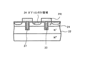
図19ではレジスト膜PRによるマスクにより選択的にボロンをイオン注入し、P+型のボディコンタクト領域34を形成した後、レジスト膜PRを除去する。
【0013】
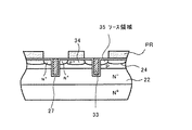
図20では新たなレジスト膜PRで予定のソース領域35およびゲート電極33を露出する様にマスクして、砒素をイオン注入し、N+型のソース領域35をトレンチ27に隣接するチャネル層24表面に形成した後、レジスト膜PRを除去する。
【0014】
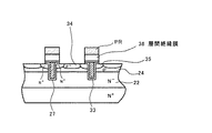
図21では、全面にNSG層を形成後、BPSG(Boron Phosphorus Silicate Glass)層をCVD法により付着して、層間絶縁膜36を形成する。その後、レジスト膜PRをマスクにして少なくともゲート電極33上に層間絶縁膜36を残して、他の領域のBPSG層、NSG層および基盤表面のゲート酸化膜を除去する。
【0015】
図22では、アルミをスパッタ装置で全面に付着して、ソース領域35およびボディコンタクト領域34にコンタクトするソース電極37を形成する。
【0016】
【特許文献1】
特開2001−284588号公報(第3頁、第19−28図)
【0017】
【発明が解決しようとする課題】
かかる従来のパワーMOSFETでは、特に微細加工技術を必要とするトレンチ形成後においても、レジスト膜を用いマスクによりパターンを形成する工程が多用されている。
【0018】
従って、セル集積度を上げてスイッチング性能の改善、特にオン抵抗の低減を実現するためにデザインルールを微細化したいが、露光装置、レジスト材、マスク作成や合わせ精度の問題で設計線幅に制限があり、レジスト膜を用いマスクによりパターンを形成する現在のデバイス設計手法では、限界にきている。
【0019】
【課題を解決するための手段】
本発明はかかる課題に鑑みてなされ、ドレイン領域となる一導電型の半導体基板と、半導体基板表面に設けた逆導電型のチャネル層と、チャネル層を貫通しドレイン領域まで到達するトレンチと、トレンチの表面に設けたゲート絶縁膜と、トレンチに埋設されその上部が基板表面から突出した半導体材料からなるゲート電極と、ゲート電極上部の層間絶縁膜と、チャネル層表面のトレンチに隣接して設けた一導電型のソース領域と、ゲート電極上部の突出部側面に形成されたサイドウォールと、隣接するトレンチ間に形成されている溝の底部でチャネル層表面に設けた逆導電型のボディコンタクト領域と、ソース領域およびボディコンタクト領域にコンタクトしたソース電極とを有する絶縁ゲート型半導体装置において、ソース領域がゲート電極上部の突出部を用いたセルフアラインにより、またボディコンタクト領域がサイドウォールを用いたセルフアラインにより形成されていることを特徴とし、セルフアラインを用いて素子を形成することにより微細化が可能となり、微細化により集積度を上げて、オン抵抗の低減を実現する絶縁ゲート型半導体装置を提供できる。
【0020】
また、ドレイン領域となる一導電型の半導体基板表面に逆導電型のチャネル層を形成する工程と、チャネル層表面に第1の絶縁膜を形成する工程と、第1の絶縁膜にトレンチ開口部を形成する工程と、トレンチ開口部の第1の絶縁膜側面に第1のサイドウォールを形成する工程と、トレンチ開口部にチャネル層を貫通しドレイン領域まで到達するトレンチを形成する工程と、トレンチの少なくともチャネル層上にゲート絶縁膜を形成する工程と、トレンチおよび第1の絶縁膜に埋設されその上部が基板表面から突出した半導体材料からなるゲート電極を形成する工程と、ゲート電極上部に層間絶縁膜を形成する工程と、ゲート電極上部を露出する工程と、チャネル層表面に一導電型の不純物領域を形成する工程と、ゲート電極上部の突出部側面に第2のサイドウォールを形成する工程と、隣接するトレンチ間に一導電型の不純物領域を貫通しチャネル層まで到達する溝を形成する工程と、溝のチャネル層表面に逆導電型の不純物領域を形成する工程と、ソース領域およびボディコンタクト領域を生成する工程と、ソース領域およびボディコンタクト領域にコンタクトしたソース電極を形成する工程とを具備することを特徴とし、セルフアラインを用いて素子を形成することにより微細化が可能となり、微細化により集積度を上げて、オン抵抗の低減を実現する絶縁ゲート型半導体装置の製造方法を提供できる。
【0021】
【発明の実施の形態】
本発明の実施の形態を図1から図15を参照してトレンチ型パワーMOSFETのNチャネル型を例に説明する。
【0022】
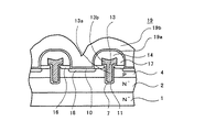
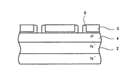
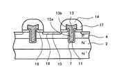
図1に本発明よるパワーMOSFETの構造の断面図を示す。
【0023】
トレンチ型パワーMOSFETは、ドレイン領域2を形成したN+型シリコン半導体基板1と、チャネル層4と、トレンチ7と、ゲート絶縁膜11と、ゲート電極13と、層間絶縁膜14と、ソース領域16と、酸化膜サイドウォール17と、ボディコンタクト領域18と、ソース電極19とから構成される。
【0024】
半導体基板は、N+型シリコン半導体基板1の上にN−型のエピタキシャル層を積層してドレイン領域2とする。
【0025】
チャネル層4は、ドレイン領域2の表面に選択的にP型のボロンをイオン注入後、拡散してトレンチ7の深さよりも浅く形成する。このチャネル層4のトレンチ7に隣接した領域に、チャネル領域(図示せず)が形成される。
【0026】
トレンチ7は、半導体基板を異方性ドライエッチングして形成し、チャネル層4を貫通してドレイン領域2まで到達させる。一般的には半導体基板上に格子状またはストライプ状にトレンチ7を形成する。トレンチ7内壁にはゲート酸化膜11を設け、ゲート電極13を形成するためにポリシリコンを埋設し、該ポリシリコンには、低抵抗化を図るためにN型不純物が導入されている。
【0027】
ゲート酸化膜11は、少なくともチャネル層と接するトレンチ7内壁に300Å前後の厚みに形成する。ゲート酸化膜11は絶縁膜であるので、トレンチ7内に設けられたゲート電極13と半導体基板に挟まれてMOS構造となっている。
【0028】
ゲート電極13は、トレンチ7に埋設されたゲート電極埋設部13aと基板表面から突出したゲート電極突出部13bで構成されており、ゲート電極突出部13bの幅はゲート電極埋設部13aの幅よりも大きく、ゲート電極突出部13b周囲の下面はゲート酸化膜11を介してチャネル層4の表面に接している。
【0029】
またゲート電極13は、半導体基板の周囲を取り巻くゲート連結電極(図示せず)まで延在され、半導体基板上に設けられたゲートパッド電極(図示せず)に連結される。ゲート電極13の上部は酸化による層間絶縁膜14が設けられるので、ゲート電極突出部13bの周端部は中央付近よりも厚く、角状になる。
【0030】
層間絶縁膜14は、全面を高温スチームに晒し、ポリシリコンで形成されているゲート電極13上部に酸化膜を成長させて形成する。
【0031】
ゲート電極突出部13b側面に形成されたサイドウォールである酸化膜サイドウォール17は、全面にCVD法によりNSG(Non−doped Silicate Glass)のCVD酸化膜を堆積後、CVD酸化膜のエッチバックにより生成する。製造方法で記載した第2のサイドウォールと一致する。
【0032】
ソース領域16は、ゲート電極突出部13bを用いたセルフアラインにより、チャネル層4表面にN+型不純物をイオン注入し、熱処理による活性化を行って形成する。またソース領域16は、ボディコンタクト領域18を形成する時に酸化膜サイドウォール17により保護されるので、酸化膜サイドウォール17の下部に設けられる構造になっている。
【0033】
ボディコンタクト領域18は、酸化膜サイドウォール17を用いたセルフアラインにより、ソース領域16を貫通しチャネル層4に到達する溝10をエッチングにより形成後、溝10の底部のチャネル層4表面にP+型不純物をイオン注入し、熱処理による活性化を行って形成する。従ってボディコンタクト領域18はソース領域16よりも下側に形成されている。またこのボディコンタクト領域の形成は、基板の電位安定化のために行うものである。
【0034】
ソース領域16およびボディコンタクト領域18にコンタクトしたソース電極19は、先ずチタンナイトライド等のバリアメタル層19aをスパッタ後さらにアルミ層19bをスパッタして形成する。
【0035】
本発明の構造による特徴は、ソース領域がゲート電極上部の突出部を用いたセルフアラインにより、またボディコンタクト領域がサイドウォールを用いたセルフアラインにより形成されていることにあり、セルフアラインを用いて素子を形成することにより微細化が可能となり、微細化により集積度を上げて、オン抵抗の低減を実現する絶縁ゲート型半導体装置を提供できる。
【0036】
次に本発明のパワーMOSFETの製造方法を図1から図15を参照してNチャネル型を例に説明する。
【0037】
トレンチ型パワーMOSFETの製造方法は、ドレイン領域2を形成したN+型シリコン半導体基板1表面に逆導電型のチャネル層4を形成する工程と、チャネル層4表面に第1の絶縁膜である窒化膜5を形成する工程と、窒化膜5にトレンチ開口部6を形成する工程と、トレンチ開口部6の窒化膜5側面に第1のサイドウォール8を形成する工程と、トレンチ開口部6にチャネル層4を貫通しドレイン領域2まで到達するトレンチ7を形成する工程と、トレンチ7の少なくともチャネル層4上にゲート酸化膜11を形成する工程と、トレンチ7および窒化膜5に埋設されその上部が基板表面から突出した半導体材料からなるゲート電極13を形成する工程と、ゲート電極13上部に層間絶縁膜14を形成する工程と、ゲート電極13上部を露出する工程と、チャネル層4表面に一導電型の不純物領域16aを形成する工程と、ゲート電極13上部の突出部側面に第2のサイドウォールである酸化膜サイドウォール17を形成する工程と、隣接するトレンチ7間に一導電型の不純物領域16aを貫通しチャネル層4まで到達する溝10を形成する工程と、溝10のチャネル層4表面に逆導電型の不純物領域18aを形成する工程と、ソース領域16およびボディコンタクト領域18を生成する工程と、ソース領域16およびボディコンタクト領域18にコンタクトしたソース電極19を形成する工程とから構成される。
【0038】
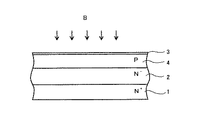
本発明の第1の工程は図2に示すごとく、ドレイン領域2を形成したN+型シリコン半導体基板1表面に逆導電型のチャネル層4を形成することにある。
【0039】
半導体基板は、N+型シリコン半導体基板1にN−型のエピタキシャル層を積層してドレイン領域2を形成する。予定のチャネル層4に選択的にボロンを注入した後、拡散してP型のチャネル層4を形成する。この時チャネル層4の表面には薄い酸化膜3が生成される。
【0040】
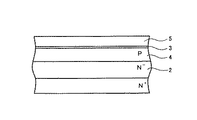
本発明の第2の工程は図3に示すごとく、チャネル層4表面に第1の絶縁膜である窒化膜5を形成することにある。
【0041】
シランガスとアンモニアガスを気相で化学反応させるCVD法により、第1の絶縁膜となるシリコン窒化膜(Si3N4)5を、半導体基板表面全面に堆積し、チャネル層4表面に窒化膜5を形成する。
【0042】
本発明の第3の工程は図4に示すごとく、窒化膜にトレンチ開口部6を形成することにある。
【0043】
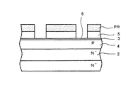
チャネル層4が露出したトレンチ開口部6を除いてレジスト膜PRによってマスクし、選択的に窒化膜5をエッチングしてチャネル層4が露出したトレンチ開口部6を形成した後、レジスト膜PRを除去する。
【0044】
本発明の第4の工程は図5に示すごとく、第1のサイドウォール8を形成することにある。
【0045】
全面にCVD法によりNSG(Non−doped Silicate Glass)のCVD酸化膜を堆積し、異方性の強いドライエッチングにより、窒化膜5の側面にのみCVD酸化膜を残すエッチバックにより、トレンチ開口部6の窒化膜5側面に第1のサイドウォール8を形成する。
【0046】
本発明の第5の工程は図6に示すごとく、チャネル層4を貫通しドレイン領域2まで到達するトレンチ7を形成することにある。
【0047】
第1のサイドウォール8をマスクとするセルフアラインでトレンチ開口部6のシリコン半導体基板をCF系およびHBr系ガスにより異方性ドライエッチングし、チャネル層4を貫通してドレイン領域2まで達するトレンチ7を形成する。
【0048】
ここでトレンチ7は第1のサイドウォール8の厚み分だけトレンチ開口部6の内側に形成されている。
【0049】
本発明の第6の工程は図7に示すごとく、トレンチ7の少なくともチャネル層4上にゲート酸化膜11を形成することにある。
【0050】
全面をダミー酸化して、トレンチ7内壁とCVD酸化膜で形成されている第1のサイドウォール8表面に酸化膜(図示せず)を形成し、その後酸化膜とCVD酸化膜で形成されている第1のサイドウォール8をエッチングによりすべて除去する。このダミー酸化を行う理由は、ドライエッチングの際のエッチングダメージを除去し、ゲート酸化膜11を安定に形成するためである。また、高温で熱酸化することによりトレンチ7の上部に丸みをつけ、トレンチ7の上部での電界集中を避ける効果もある。
【0051】
その後全面を熱酸化して、ゲート絶縁膜となる厚さ300Å前後のゲート酸化膜11を形成する。
【0052】
本発明の第7の工程は図8に示すごとく、トレンチ7および窒化膜5に埋設されその上部が基板表面から突出した半導体材料からなるゲート電極13を形成することにある。
【0053】
全面にノンドープのポリシリコン層を付着し、リンを高濃度に注入・拡散して高導電率化を図る。その後全面に付着したポリシリコン層をマスクなしでドライエッチングして、トレンチ7に埋設されたゲート電極埋設部13aと基板表面から突出し窒化膜5内に埋設されたゲート電極突出部13bで構成されているゲート電極13を形成する。
【0054】
ゲート電極突出部13bは第1のサイドウォール8を除去した窒化膜5に埋設されているので、13bの幅はトレンチ7に埋設されるゲート電極埋設部13aの幅よりも大きく、ゲート電極突出部13b周囲の下面はゲート酸化膜11を介してチャネル層4の表面に接している。
【0055】
本発明の第8の工程は図9に示すごとく、ゲート電極13上部に層間絶縁膜14を形成することにある。
【0056】
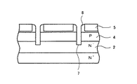
窒化膜5に埋設されたゲート電極13を新たにマスクを用いることなく全面を高温スチームに晒し、ポリシリコンで形成されているゲート電極13上部表面に酸化膜を成長させ、層間絶縁膜14とする。
【0057】
本発明の第9の工程は図10に示すごとく、ゲート電極13上部を露出することにある。
【0058】
層間絶縁膜14を形成後、酸化膜ライトエッチを行い、窒化膜5上の微量な酸化膜を除去すると共に、酸化膜で形成されている層間絶縁膜14も少しエッチングされて酸化膜厚が減少する。この状態で窒化膜5のエッチングを行うと窒化膜サイドウォールが形成されることなく、窒化膜5が全面除去され、ゲート電極突出部13bが露出する。
【0059】
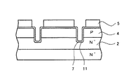
本発明の第10の工程は図11に示すごとく、チャネル層4表面に、完成時ソース領域16となる一導電型の不純物領域16aを形成することにある。
【0060】
全面に砒素をドーズ量5.0×10¹⁵でイオン注入すると、ゲート電極突出部13bをマスクとして用いたセルフアラインにより、トレンチ7間のチャネル層4の表面に、完成時ソース領域16となる浅いN+型の不純物領域である、一導電型の不純物領域16aが形成される。また、全面にイオン注入することにより、ゲート電極13にもN+型の不純物が導入されるが、ゲート電極13の高電導率化を図るために拡散されている不純物と同型なので、何ら影響はない。
【0061】
本発明の第11の工程は図12に示すごとく、ゲート電極突出部13b側面に第2のサイドウォールである酸化膜サイドウォール17を形成することにある。
【0062】
全面にCVD法によりNSG(Non−doped Silicate Glass)のCVD酸化膜を堆積し、異方性の強いドライエッチングにより、ゲート電極突出部13bの側面にCVD酸化膜を残すエッチバックにより、第2のサイドウォールとなる酸化膜サイドウォール17を形成する。
【0063】
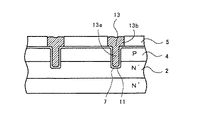
ここで、第9の工程において窒化膜5を全面除去してゲート電極突出部13bを露出した時は、ゲート電極突出部13bの側面が露出していたが、酸化膜サイドウォール17を形成することによりゲート電極突出部13bは、すべて絶縁膜で覆われることになる。ゲート電極突出部13b上部表面は層間絶縁膜14で覆われたままである。
【0064】
本発明の第12の工程は図13に示すごとく、隣接するトレンチ7間に、一導電型の不純物領域16aを貫通しチャネル層4まで到達する溝10を形成することにある。
【0065】
酸化膜サイドウォール17をマスクとして用いたセルフアラインにより、隣接するトレンチ7間に露出しているシリコン半導体基板を、CF系およびHBr系ガスにより異方性ドライエッチングし、少なくても一導電型の不純物領域16aを貫通しチャネル層4に到達する深さまでエッチングして、溝10を形成する。
【0066】
本発明の第13の工程は図14に示すごとく、溝10部分のチャネル層4表面に、完成時ボディコンタクト領域18となる逆導電型の不純物領域18aを形成することにある。
【0067】
全面にボロンをドーズ量5.0×10¹⁴でイオン注入すると、酸化膜サイドウォール17をマスクとして用いたセルフアラインにより、溝10のチャネル層4の表面に、完成時ボディコンタクト領域18となる浅いP+型の不純物領域である、逆導電型の不純物領域18aが形成される。ボディコンタクト領域18はドレイン領域2とチャネル層4で形成される基板の電位安定化のために形成される。
【0068】
本発明の第14の工程は図15に示すごとく、イオン注入した一導電型の不純物領域16aおよび逆導電型の不純物領域18aを活性化して、それぞれソース領域16およびボディコンタクト領域18を生成することにある。
【0069】
イオン注入した浅いN+型の不純物領域である一導電型の不純物領域16aおよび浅いP+型の不純物領域である逆導電型の不純物領域18aの活性化、シリコン結晶のダメージの回復などを目的とした熱処理であるリフローを実施する。
【0070】
リフロー処理により、一導電型の不純物領域16aは活性化されたソース領域16に、逆導電型の不純物領域18aは活性化されたボディコンタクト領域18となる。
【0071】
本発明の第15の工程は図1に示すごとく、全面にソース電極19を形成することにある。
【0072】
リフロー処理により生成したソース領域16およびボディコンタクト領域18の表面の薄い酸化膜を除去するためにウエットエッチングを行ってから、先ずチタンナイトライド等のバリアメタル層19aをスパッタ後、さらにアルミ層19bをスパッタして、ソース領域16およびボディコンタクト領域18に電気的に接続されたソース電極19を全面に形成する。
【0073】
【発明の効果】
本発明の絶縁ゲート型半導体装置およびその製造方法によれば以下にあげる数々の効果が得られる。
【0074】
第1に、ゲート電極の形状に特徴があり、ゲート電極トレンチ埋設部分の上部に突出部を設け、突出部表面以外を窒化膜に埋設された状態で形成することにより、層間絶縁膜をマスクを用いることなくゲート電極上部の酸化のみで形成していること、ゲート電極突出部を露出し、露出したゲート電極突出部を用いたセルフアラインでソース領域を形成していること、またゲート電極突出部側面に形成したサイドウォールを用いたセルフアラインでボディコンタクト領域を形成していることに示されるように基本となる素子の形成において、従来のマスクを用いた製造方法によらず、ゲート電極突出部やその側面に形成したサイドウォールを用いたセルフアラインによる製造方法を用いているので、マスク合わせの余裕をとらずに精度の高いパターン重ね合わせが実現でき、デザインルールをより微細化することができる。従って集積度を上げることができるので、セル密度の向上を図ることができ、オン抵抗の低減に大きく寄与できる。
【0075】
ちなみに従来のデザインルールと本発明によるデザインルールで、セル密度を比較してみると約1.42倍に向上している。
【0076】
第2に、パターン形成時の位置合わせのズレが発生しないので、従来発生していたマスクズレによる特性のバラツキ、信頼性不良および製造ラインの歩留まりの低下などが大幅に改善される。
【図面の簡単な説明】
【図1】本発明の絶縁ゲート型半導体装置およびその製造方法を説明する断面図である。
【図2】本発明の絶縁ゲート型半導体装置の製造方法を説明する断面図である。
【図3】本発明の絶縁ゲート型半導体装置の製造方法を説明する断面図である。
【図4】本発明の絶縁ゲート型半導体装置の製造方法を説明する断面図である。
【図5】本発明の絶縁ゲート型半導体装置の製造方法を説明する断面図である。
【図6】本発明の絶縁ゲート型半導体装置の製造方法を説明する断面図である。
【図7】本発明の絶縁ゲート型半導体装置の製造方法を説明する断面図である。
【図8】本発明の絶縁ゲート型半導体装置の製造方法を説明する断面図である。
【図9】本発明の絶縁ゲート型半導体装置の製造方法を説明する断面図である。
【図10】本発明の絶縁ゲート型半導体装置の製造方法を説明する断面図である。
【図11】本発明の絶縁ゲート型半導体装置の製造方法を説明する断面図である。
【図12】本発明の絶縁ゲート型半導体装置の製造方法を説明する断面図である。
【図13】本発明の絶縁ゲート型半導体装置の製造方法を説明する断面図である。
【図14】本発明の絶縁ゲート型半導体装置の製造方法を説明する断面図である。
【図15】本発明の絶縁ゲート型半導体装置の製造方法を説明する断面図である。
【図16】従来の絶縁ゲート型半導体装置の製造方法を説明する断面図である。
【図17】従来の絶縁ゲート型半導体装置の製造方法を説明する断面図である。
【図18】従来の絶縁ゲート型半導体装置の製造方法を説明する断面図である。
【図19】従来の絶縁ゲート型半導体装置の製造方法を説明する断面図である。
【図20】従来の絶縁ゲート型半導体装置の製造方法を説明する断面図である。
【図21】従来の絶縁ゲート型半導体装置の製造方法を説明する断面図である。
【図22】従来の絶縁ゲート型半導体装置およびその製造方法を説明する断面図である。
【符号の説明】
1 N+型シリコン半導体基板
2 ドレイン領域
3 薄い酸化膜
4 チャネル層
5 窒化膜
6 トレンチ開口部
7 トレンチ
8 第1のサイドウォール
10 溝
11 ゲート酸化膜
13 ゲート電極
13a ゲート電極埋設部
13b ゲート電極突出部
14 層間絶縁膜
16 ソース領域
16a 一導電型の不純物領域
17 酸化膜サイドウォール
18 ボディコンタクト領域
18a 逆導電型の不純物領域
19 ソース電極
19a バリアメタル層
19b アルミ層
20 パシベーション膜[0001]
TECHNICAL FIELD OF THE INVENTION
The present invention relates to an insulated gate semiconductor device and a method of manufacturing the same, and more particularly, to an insulated gate semiconductor device that improves switching performance by increasing cell integration using self-alignment, and in particular, realizes reduction of on-resistance and a method of manufacturing the same.
[0002]
[Prior art]
With the spread of mobile terminals, small-sized and large-capacity lithium-ion batteries have been required. The protection circuit that performs the battery management of the charging and discharging of the lithium ion battery must be small and sufficiently resistant to a load short due to the need for reducing the weight of the portable terminal. Such a protection circuit is required to be miniaturized because it is built in the container of the lithium ion battery, and COB (Chip on Board) technology using a lot of chip components has been used to meet the demand for miniaturization. However, on the other hand, since the power MOSFET is connected in series to the lithium ion battery, there is a need to make the on-resistance of the power MOSFET extremely small, which is an essential element for a mobile phone to increase the talk time and the standby time.
[0003]
For this reason, development for increasing the cell density by fine processing in manufacturing chips has been promoted. Specifically, in the planar structure in which the channel is formed on the surface of the semiconductor substrate, the cell density is 7.4 million cells / square inch, but in the first generation of the trench structure in which the channel is formed on the side surface of the trench, the cell density is 2500. Significantly improved to 10,000 units / square inch. Further, in the second generation of the trench structure, the cell density could be improved to 72 million cells / square inch by miniaturization (for example, see Patent Document 1).
[0004]
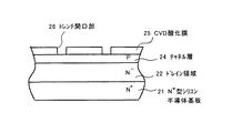
FIG. 22 shows an example of a conventional trench-structured power MOSFET of an N-channel type.
[0005]
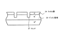
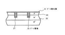
A
[0006]
With reference to FIGS. 16 to 22, a manufacturing process of a conventional N-channel power MOSFET having a trench structure will be described.
[0007]
In FIG. 16, an N − type epitaxial layer is stacked on an N + type silicon semiconductor substrate 21 to form a
[0008]
An NSG (Non-Doped Silicate Glass) CVD oxide film 25 is formed on the entire surface by a CVD method, and is partially removed by dry etching after forming a mask to form a trench opening 26 where the
[0009]
In FIG. 17, the silicon semiconductor substrate in the trench opening 26 is anisotropically dry-etched with CF-based and HBr-based gases using the CVD oxide film 25 as a mask to form a
[0010]
Next, an oxide film (not shown) is formed on the inner wall of the
[0011]
In FIG. 18, a gate oxide film 31 is formed by thermally oxidizing the entire surface. Thereafter, a
[0012]
In FIG. 19, boron ions are selectively implanted using a mask made of a resist film PR to form a P + type
[0013]
In FIG. 20, arsenic is ion-implanted by masking a new resist film PR so as to expose the intended
[0014]
In FIG. 21, after an NSG layer is formed on the entire surface, a BPSG (Boron Phosphorus Silicate Glass) layer is attached by a CVD method to form an interlayer insulating film 36. After that, using the resist film PR as a mask, the BPSG layer, the NSG layer, and the gate oxide film on the substrate surface in other regions are removed, leaving at least the interlayer insulating film 36 on the
[0015]
In FIG. 22, aluminum is deposited on the entire surface by a sputtering apparatus to form a source electrode 37 that contacts the
[0016]
[Patent Document 1]
JP 2001-284588 A (Page 3, FIGS. 19-28)
[0017]
[Problems to be solved by the invention]
In such a conventional power MOSFET, a step of forming a pattern using a mask using a resist film is often used, especially after forming a trench that requires fine processing technology.
[0018]
Therefore, we want to refine the design rules in order to increase the cell integration and improve the switching performance, especially to reduce the on-resistance. However, the design line width is limited due to the problems of the exposure equipment, resist material, mask preparation and alignment accuracy. The current device design method of forming a pattern using a mask using a resist film has reached its limit.
[0019]
[Means for Solving the Problems]
The present invention has been made in view of the above problems, and has been made in consideration of the above circumstances, a semiconductor substrate of one conductivity type serving as a drain region, a channel layer of an opposite conductivity type provided on a surface of the semiconductor substrate, a trench penetrating the channel layer and reaching the drain region, and a trench. A gate insulating film provided on the surface of the substrate, a gate electrode made of a semiconductor material buried in the trench and having an upper portion protruding from the substrate surface, an interlayer insulating film on the gate electrode, and a trench provided on the channel layer surface adjacent to the trench. A source region of one conductivity type, a sidewall formed on the side surface of the protrusion above the gate electrode, and a body contact region of the opposite conductivity type provided on the surface of the channel layer at the bottom of the groove formed between adjacent trenches; An insulated gate semiconductor device having a source region, a source electrode in contact with a body contact region, and a source region. It is characterized by the self-alignment using the protruding part at the top and the body contact region formed by self-alignment using the sidewall.It is possible to miniaturize by forming the element using the self-alignment. In addition, it is possible to provide an insulated gate semiconductor device capable of increasing the degree of integration by miniaturization and reducing on-resistance.
[0020]
A step of forming a channel layer of the opposite conductivity type on a surface of the semiconductor substrate of one conductivity type serving as a drain region; a step of forming a first insulating film on the surface of the channel layer; and a step of forming a trench opening in the first insulating film. Forming a first sidewall on the side surface of the first insulating film in the trench opening; forming a trench in the trench opening through the channel layer to reach the drain region; Forming a gate insulating film on at least the channel layer, forming a gate electrode made of a semiconductor material buried in the trench and the first insulating film and having an upper part protruding from the substrate surface; Forming an insulating film, exposing the upper part of the gate electrode, forming an impurity region of one conductivity type on the surface of the channel layer, Forming a second sidewall between adjacent trenches, forming a groove between adjacent trenches through the one conductivity type impurity region and reaching the channel layer, and forming a reverse conductivity type impurity region on the channel layer surface of the groove. Forming a source region and a body contact region; and forming a source electrode in contact with the source region and the body contact region. By doing so, it is possible to provide a method of manufacturing an insulated gate semiconductor device that can achieve miniaturization, increase the degree of integration by miniaturization, and reduce on-resistance.
[0021]
BEST MODE FOR CARRYING OUT THE INVENTION
An embodiment of the present invention will be described with reference to FIGS. 1 to 15 taking an N-channel trench MOSFET as an example.
[0022]
FIG. 1 shows a sectional view of the structure of a power MOSFET according to the present invention.
[0023]
The trench type power MOSFET includes an N + type silicon semiconductor substrate 1 having a
[0024]
The semiconductor substrate is formed as a
[0025]
The
[0026]
The
[0027]
[0028]
The
[0029]
The
[0030]
The
[0031]
The
[0032]
The
[0033]
The
[0034]
The source electrode 19 in contact with the
[0035]
The feature of the structure of the present invention resides in that the source region is formed by self-alignment using the protrusion above the gate electrode, and the body contact region is formed by self-alignment using the sidewall. By forming the element, miniaturization becomes possible, and the degree of integration can be increased by miniaturization to provide an insulated gate semiconductor device that realizes a reduction in on-resistance.
[0036]
Next, a method of manufacturing a power MOSFET according to the present invention will be described with reference to FIGS.
[0037]
The method of manufacturing the trench type power MOSFET includes a step of forming a
[0038]
The first step of the present invention is to form a
[0039]
In the semiconductor substrate, an N − type epitaxial layer is stacked on an N + type silicon semiconductor substrate 1 to form a
[0040]
The second step of the present invention is to form a
[0041]
A silicon nitride film (Si3N4) 5 serving as a first insulating film is deposited on the entire surface of the semiconductor substrate by a CVD method in which a silane gas and an ammonia gas are chemically reacted in a gas phase, and a
[0042]
The third step of the present invention is to form a
[0043]
After masking with the resist film PR except for the
[0044]
The fourth step of the present invention is to form the
[0045]
An NSG (Non-doped Silicate Glass) CVD oxide film is deposited on the entire surface by the CVD method, and the
[0046]
The fifth step of the present invention is to form a
[0047]
The silicon semiconductor substrate in the
[0048]
Here, the
[0049]
The sixth step of the present invention is to form a
[0050]
An entire surface is subjected to dummy oxidation to form an oxide film (not shown) on the inner wall of the
[0051]
Thereafter, the entire surface is thermally oxidized to form a
[0052]
As shown in FIG. 8, the seventh step of the present invention is to form a
[0053]
A non-doped polysilicon layer is attached to the entire surface, and phosphorus is injected and diffused at a high concentration to achieve high conductivity. Thereafter, the polysilicon layer adhered to the entire surface is dry-etched without a mask to form a gate electrode buried
[0054]
Since the
[0055]
The eighth step of the present invention is to form an
[0056]
The entire surface of the
[0057]
The ninth step of the present invention is to expose the upper part of the
[0058]
After forming the
[0059]
The tenth step of the present invention is to form a one conductivity
[0060]
When arsenic is ion-implanted over the entire surface at a dose of 5.0 × 10 15 , the surface of the
[0061]
As shown in FIG. 12, the eleventh step of the present invention is to form an
[0062]
An NSG (Non-doped Silicate Glass) CVD oxide film is deposited on the entire surface by the CVD method, and the second anisotropic dry etching is performed to leave the CVD oxide film on the side surface of the gate
[0063]
Here, when the entire surface of the
[0064]
In the twelfth step of the present invention, as shown in FIG. 13, a
[0065]
The silicon semiconductor substrate exposed between the
[0066]
As shown in FIG. 14, the thirteenth step of the present invention is to form an
[0067]
When boron is ion-implanted into the entire surface at a dose of 5.0 × 10 14 , a shallow
[0068]
In a fourteenth step of the present invention, the
[0069]
The purpose is to activate the one conductivity
[0070]
By the reflow process, the one conductivity
[0071]
The fifteenth step of the present invention is to form a
[0072]
After performing wet etching to remove a thin oxide film on the surface of the
[0073]
【The invention's effect】
According to the insulated gate semiconductor device and the method of manufacturing the same of the present invention, the following effects can be obtained.
[0074]
First, the shape of the gate electrode is characterized by providing a protrusion above the gate electrode trench buried portion and forming the portion other than the protrusion surface in a state buried in the nitride film, thereby masking the interlayer insulating film. That the gate electrode is formed only by oxidizing the upper part without using it, that the gate electrode protrusion is exposed, and that the source region is formed by self-alignment using the exposed gate electrode protrusion, and that the gate electrode protrusion is formed. In the formation of the basic element, as shown in the fact that the body contact region is formed by self-alignment using the sidewall formed on the side surface, regardless of the conventional manufacturing method using a mask, the gate electrode protruding portion is formed. And a self-aligned manufacturing method using sidewalls formed on the side surfaces of the mask. Over emissions superposition can be realized, it can be finer design rules. Therefore, the degree of integration can be increased, so that the cell density can be improved and the on-resistance can be greatly reduced.
[0075]
Incidentally, when the cell density is compared between the conventional design rule and the design rule according to the present invention, the cell density is improved by about 1.42 times.
[0076]
Second, since there is no misalignment at the time of pattern formation, variations in characteristics due to mask misalignment, poor reliability and reduced production line yield, which have conventionally occurred, are greatly improved.
[Brief description of the drawings]
FIG. 1 is a cross-sectional view illustrating an insulated gate semiconductor device and a method for manufacturing the same of the present invention.
FIG. 2 is a cross-sectional view illustrating a method of manufacturing an insulated gate semiconductor device of the present invention.
FIG. 3 is a cross-sectional view illustrating a method of manufacturing an insulated gate semiconductor device of the present invention.
FIG. 4 is a cross-sectional view illustrating the method of manufacturing the insulated gate semiconductor device of the present invention.
FIG. 5 is a sectional view illustrating the method of manufacturing the insulated gate semiconductor device of the present invention.
FIG. 6 is a sectional view illustrating the method of manufacturing the insulated gate semiconductor device of the present invention.
FIG. 7 is a cross-sectional view illustrating the method of manufacturing the insulated gate semiconductor device of the present invention.
FIG. 8 is a sectional view illustrating the method of manufacturing the insulated gate semiconductor device of the present invention.
FIG. 9 is a sectional view illustrating the method of manufacturing the insulated gate semiconductor device of the present invention.
FIG. 10 is a sectional view illustrating the method of manufacturing the insulated gate semiconductor device of the present invention.
FIG. 11 is a sectional view illustrating the method of manufacturing the insulated gate semiconductor device of the present invention.
FIG. 12 is a sectional view illustrating the method of manufacturing the insulated gate semiconductor device of the present invention.
FIG. 13 is a sectional view illustrating the method of manufacturing the insulated gate semiconductor device of the present invention.
FIG. 14 is a sectional view illustrating the method of manufacturing the insulated gate semiconductor device of the present invention.
FIG. 15 is a sectional view illustrating the method of manufacturing the insulated gate semiconductor device of the present invention.
FIG. 16 is a cross-sectional view illustrating a method of manufacturing a conventional insulated gate semiconductor device.
FIG. 17 is a cross-sectional view illustrating a method of manufacturing a conventional insulated gate semiconductor device.
FIG. 18 is a cross-sectional view illustrating a method for manufacturing a conventional insulated gate semiconductor device.
FIG. 19 is a cross-sectional view illustrating a method of manufacturing a conventional insulated gate semiconductor device.
FIG. 20 is a cross-sectional view illustrating a method for manufacturing a conventional insulated gate semiconductor device.
FIG. 21 is a cross-sectional view illustrating a method of manufacturing a conventional insulated gate semiconductor device.
FIG. 22 is a cross-sectional view illustrating a conventional insulated gate semiconductor device and a method for manufacturing the same.
[Explanation of symbols]
Reference Signs List 1 N + type
Claims (18)
前記半導体基板表面に設けた逆導電型のチャネル層と、
前記チャネル層を貫通し前記ドレイン領域まで到達するトレンチと、
前記トレンチの表面に設けたゲート絶縁膜と、
前記トレンチに埋設されその上部が基板表面から突出した半導体材料からなるゲート電極と、
前記ゲート電極上部の層間絶縁膜と、
前記チャネル層表面の前記トレンチに隣接して設けた一導電型のソース領域と、
前記ゲート電極上部の突出部側面に形成されたサイドウォールと、
隣接する前記トレンチ間に形成されている溝の底部で前記チャネル層表面に設けた逆導電型のボディコンタクト領域と、
前記ソース領域および前記ボディコンタクト領域にコンタクトしたソース電極とを具備することを特徴とする絶縁ゲート型半導体装置。A semiconductor substrate of one conductivity type serving as a drain region,
A channel layer of the opposite conductivity type provided on the surface of the semiconductor substrate,
A trench penetrating the channel layer and reaching the drain region;
A gate insulating film provided on the surface of the trench;
A gate electrode made of a semiconductor material buried in the trench and having an upper part protruding from the substrate surface;
An interlayer insulating film on the gate electrode,
A source region of one conductivity type provided adjacent to the trench on the surface of the channel layer;
A sidewall formed on a side surface of the protrusion above the gate electrode;
An opposite conductivity type body contact region provided on the surface of the channel layer at the bottom of the groove formed between the adjacent trenches;
An insulated gate semiconductor device comprising: a source electrode in contact with the source region and the body contact region.
前記チャネル層表面に第1の絶縁膜を形成する工程と、
前記第1の絶縁膜にトレンチ開口部を形成する工程と、
前記トレンチ開口部の第1の絶縁膜側面に第1のサイドウォールを形成する工程と、
前記トレンチ開口部に前記チャネル層を貫通し前記ドレイン領域まで到達するトレンチを形成する工程と、
前記トレンチの少なくとも前記チャネル層上にゲート絶縁膜を形成する工程と、
前記トレンチおよび前記第1の絶縁膜に埋設されその上部が基板表面から突出した半導体材料からなるゲート電極を形成する工程と、
前記ゲート電極上部に層間絶縁膜を形成する工程と、
前記ゲート電極上部を露出する工程と、
前記チャネル層表面に一導電型の不純物領域を形成する工程と、
前記ゲート電極上部の突出部側面に第2のサイドウォールを形成する工程と、
隣接する前記トレンチ間に前記一導電型の不純物領域を貫通しチャネル層まで到達する溝を形成する工程と、
前記溝のチャネル層表面に逆導電型の不純物領域を形成する工程と、
ソース領域およびボディコンタクト領域を生成する工程と、
前記ソース領域および前記ボディコンタクト領域にコンタクトしたソース電極を形成する工程とを具備することを特徴とする絶縁ゲート型半導体装置の製造方法。Forming a channel layer of the opposite conductivity type on the surface of the semiconductor substrate of the one conductivity type serving as the drain region,
Forming a first insulating film on the surface of the channel layer;
Forming a trench opening in the first insulating film;
Forming a first sidewall on a side surface of a first insulating film of the trench opening;
Forming a trench through the channel layer in the trench opening to reach the drain region;
Forming a gate insulating film on at least the channel layer of the trench;
Forming a gate electrode made of a semiconductor material buried in the trench and the first insulating film and having an upper part protruding from a substrate surface;
Forming an interlayer insulating film over the gate electrode;
Exposing the upper portion of the gate electrode;
Forming an impurity region of one conductivity type on the surface of the channel layer;
Forming a second sidewall on a side surface of the protrusion above the gate electrode;
Forming a groove between the adjacent trenches and penetrating the impurity region of one conductivity type and reaching the channel layer;
Forming a reverse conductivity type impurity region on the channel layer surface of the trench;
Generating a source region and a body contact region;
Forming a source electrode in contact with the source region and the body contact region.
Priority Applications (1)
| Application Number | Priority Date | Filing Date | Title |
|---|---|---|---|
| JP2002272389A JP2004111663A (en) | 2002-09-19 | 2002-09-19 | Insulated gate semiconductor device and method of manufacturing the same |
Applications Claiming Priority (1)
| Application Number | Priority Date | Filing Date | Title |
|---|---|---|---|
| JP2002272389A JP2004111663A (en) | 2002-09-19 | 2002-09-19 | Insulated gate semiconductor device and method of manufacturing the same |
Publications (1)
| Publication Number | Publication Date |
|---|---|
| JP2004111663A true JP2004111663A (en) | 2004-04-08 |
Family
ID=32269414
Family Applications (1)
| Application Number | Title | Priority Date | Filing Date |
|---|---|---|---|
| JP2002272389A Pending JP2004111663A (en) | 2002-09-19 | 2002-09-19 | Insulated gate semiconductor device and method of manufacturing the same |
Country Status (1)
| Country | Link |
|---|---|
| JP (1) | JP2004111663A (en) |
Cited By (5)
| Publication number | Priority date | Publication date | Assignee | Title |
|---|---|---|---|---|
| JP2007110071A (en) * | 2005-09-16 | 2007-04-26 | Denso Corp | Semiconductor device manufacturing method and semiconductor device |
| JP2008042056A (en) * | 2006-08-09 | 2008-02-21 | Renesas Technology Corp | Semiconductor device and manufacturing method thereof |
| JP2008519436A (en) * | 2004-10-29 | 2008-06-05 | インターナショナル レクティファイアー コーポレイション | MOSFET having trenches deposited with a filling oxide layer |
| JP2008235399A (en) * | 2007-03-19 | 2008-10-02 | Toshiba Corp | Trench type power semiconductor device and manufacturing method thereof |
| JP2009224543A (en) * | 2008-03-17 | 2009-10-01 | Sony Corp | Method for production of semiconductor device |
-
2002
- 2002-09-19 JP JP2002272389A patent/JP2004111663A/en active Pending
Cited By (6)
| Publication number | Priority date | Publication date | Assignee | Title |
|---|---|---|---|---|
| JP2008519436A (en) * | 2004-10-29 | 2008-06-05 | インターナショナル レクティファイアー コーポレイション | MOSFET having trenches deposited with a filling oxide layer |
| US8106446B2 (en) | 2004-10-29 | 2012-01-31 | International Rectifier Corporation | Trench MOSFET with deposited oxide |
| JP2007110071A (en) * | 2005-09-16 | 2007-04-26 | Denso Corp | Semiconductor device manufacturing method and semiconductor device |
| JP2008042056A (en) * | 2006-08-09 | 2008-02-21 | Renesas Technology Corp | Semiconductor device and manufacturing method thereof |
| JP2008235399A (en) * | 2007-03-19 | 2008-10-02 | Toshiba Corp | Trench type power semiconductor device and manufacturing method thereof |
| JP2009224543A (en) * | 2008-03-17 | 2009-10-01 | Sony Corp | Method for production of semiconductor device |
Similar Documents
| Publication | Publication Date | Title |
|---|---|---|
| JP4829473B2 (en) | Insulated gate semiconductor device and manufacturing method thereof | |
| US9299794B2 (en) | Semiconductor device | |
| KR20030032118A (en) | Method for fabricating trench-gated power semiconductor device | |
| US20210343865A1 (en) | Semiconductor structure and method for forming same | |
| CN108155237A (en) | A kind of semiconductor devices and its manufacturing method and electronic device | |
| JPH1197629A (en) | Semiconductor device and manufacturing method thereof | |
| JP3754266B2 (en) | Insulated gate type semiconductor device manufacturing method | |
| CN103178013B (en) | The manufacture method of semiconductor device | |
| TWI236090B (en) | Trench power MOSFET and method for fabricating the same | |
| JP2001274396A (en) | Manufacturing method of insulated gate semiconductor device | |
| CN118431290A (en) | Trench type power device, preparation method, power module, conversion circuit and vehicle | |
| JP4906184B2 (en) | Insulated gate type semiconductor device manufacturing method | |
| JP2004111663A (en) | Insulated gate semiconductor device and method of manufacturing the same | |
| JP2002314065A (en) | MOS semiconductor device and method of manufacturing the same | |
| JP4454213B2 (en) | Insulated gate type semiconductor device manufacturing method | |
| JPH053300A (en) | Semiconductor device | |
| JPH11154749A (en) | Semiconductor device and manufacturing method thereof | |
| JP2004111662A (en) | Insulated gate semiconductor device and method of manufacturing the same | |
| JP4093712B2 (en) | Insulated gate type semiconductor device manufacturing method | |
| JP3953280B2 (en) | Insulated gate type semiconductor device manufacturing method | |
| JP2001320051A (en) | Insulated gate type semiconductor device | |
| JP2002158233A (en) | Method for manufacturing insulated gate semiconductor device | |
| JP2004111660A (en) | Manufacturing method of insulated gate semiconductor device | |
| TWI405326B (en) | Double-conducting semiconductor device and manufacturing method thereof | |
| JP2004349329A (en) | Method for manufacturing insulated gate type semiconductor device |