JP2004095612A - Semiconductor device and wiring board - Google Patents
Semiconductor device and wiring board Download PDFInfo
- Publication number
- JP2004095612A JP2004095612A JP2002250934A JP2002250934A JP2004095612A JP 2004095612 A JP2004095612 A JP 2004095612A JP 2002250934 A JP2002250934 A JP 2002250934A JP 2002250934 A JP2002250934 A JP 2002250934A JP 2004095612 A JP2004095612 A JP 2004095612A
- Authority
- JP
- Japan
- Prior art keywords
- wiring board
- semiconductor device
- core material
- bonding
- semiconductor element
- Prior art date
- Legal status (The legal status is an assumption and is not a legal conclusion. Google has not performed a legal analysis and makes no representation as to the accuracy of the status listed.)
- Pending
Links
Images


Classifications
-
- H—ELECTRICITY
- H01—ELECTRIC ELEMENTS
- H01L—SEMICONDUCTOR DEVICES NOT COVERED BY CLASS H10
- H01L2224/00—Indexing scheme for arrangements for connecting or disconnecting semiconductor or solid-state bodies and methods related thereto as covered by H01L24/00
- H01L2224/73—Means for bonding being of different types provided for in two or more of groups H01L2224/10, H01L2224/18, H01L2224/26, H01L2224/34, H01L2224/42, H01L2224/50, H01L2224/63, H01L2224/71
- H01L2224/732—Location after the connecting process
- H01L2224/73201—Location after the connecting process on the same surface
- H01L2224/73203—Bump and layer connectors
- H01L2224/73204—Bump and layer connectors the bump connector being embedded into the layer connector
Abstract
Description
【0001】
【発明の属する技術分野】
本発明は半導体装置に係り、特に超音波を用いたフリップチップ接合により半導体素子を配線基板に接続して形成される半導体装置に関する。
【0002】
【従来の技術】
半導体装置としての外部接続端子を設けるために、いわゆるインターポーザと呼ばれる配線基板により配線の引き回しを行い、外部接続端子を効率的に配列した半導体パッケージが多くなっている。このような半導体パッケージを製造する工程において、半導体素子を配線基板に搭載する際に、超音波を用いて半導体素子のバンプを配線基板の電極に接合する、いわゆる超音波フリップチップボンディングが多く用いられる。
【0003】
近年、半導体素子の高機能化に伴い半導体素子のサイズが増大しており、大型の半導体素子に対応したフリップチップボンディング用の大型の超音波振動工具がいくつか開発されている。これにより、大型の半導体素子も超音波フリップチップボンディングにより実装されるようになってきている。
【0004】
半導体素子がフリップチップ実装される配線基板としては、セラミック基板、樹脂テープ基板、有機基板等が用いられる。このうち、例えばガラスエポキシ基板のような有機基板は、取り扱いやコストの面で他の基板より優れており、多く使用されている。
【0005】
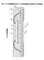
図1は従来の両面配線型の配線基板の断面図である。図1に示す配線基板1は、基板コア材2の両面に導体パターンが形成されている。半導体素子が搭載される面側の導体パターンにより、半導体素子の電極(バンプ)をフリップチップ接合するためのボンディングパッド3と、上部配線4とが形成される。また、反対側の面の導体パターンにより、外部接続端子を設けるためのランド5と、下部配線6とが形成される。また、基板コア材2を貫通して両側の導体パターンを電気的に接続する貫通ビア(図示せず)が設けられ、ボンディングパッド3は、上部配線4、貫通ビア及び下部配線6を介して、ランド5に接続される。ランド5には外部接続端子としてハンダボール等が設けられる。基板コア材2は、一般的にFR−4材やBTレジンのような有機材料用いて形成されることが多い。なお、両面の導体パターンの露出する必要のない部分はソルダレジスト7により覆われる。
【0006】
図2は従来の片面配線型の配線基板の断面図である。図2に示す配線基板11は、基板コア材12の片面だけに導体パターンが形成されている。導体パターンにより、半導体素子の電極(バンプ)をフリップチップ接合するためのボンディングパッド13と、配線14と、外部接続端子を設けるためのランド15とが形成される。ランド15の下には、基板コア材12を貫通して裏面まで延在する貫通孔16が形成されており、貫通孔16を介してハンダボール等の外部接続端子がランド15に接続される。図1に示す配線基板1と同様に、基板コア材12は、FR−4材やBTレジンのような有機材料を用いて形成されることが多い。
【0007】
【発明が解決しようとする課題】
図1及び2に示す配線基板1又は11に対して、半導体素子をフリップチップ搭載する際には、半導体素子をボンディングツールに装着して、半導体素子のバンプを配線基板のボンディングパッド3又は13に押圧しながらボンディングツールから超音波振動を印加する。
【0008】
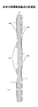
図3は図1に示す配線基板1に対して半導体素子10を超音波フリップチップボンディングする工程を説明するための図である。図3(a)に示すように、配線基板1はボンディングステージ20上に載置され、真空吸引チャック等で固定される。また、配線基板1の固定を確実にするために、配線基板1の外周はクランプ治具21により固定される。一方、搭載される半導体素子22は、その背面がボンディングツール23に固定された状態で、バンプ22aと配線基板1のボンディングパッド3との位置合わせが行われる。
【0009】
位置合わせが完了すると、図3(b)に示すように、半導体素子22のバンプが配線基板1のボンディングパッドに押圧される。この状態で、ボンディングツール23から半導体素子に対して超音波振動が印加される。これにより、バンプ22aが超音波振動し、バンプ22aはボンディングパッドに超音波接合される。
【0010】
ここで、従来の配線基板1の下面側にはランド5及び配線部分が形成されているため、上面側のボンディングパッド3の直下において、基板コア材2とボンディングステージ20との間に隙間が形成される場合がある。隙間が形成された状態で、ボンディングパッド3上の電極22が超音波振動すると、配線基板1に微小なたわみが生じ、超音波振動エネルギの一部が配線基板1に吸収・拡散されてしまう。このような場合、超音波接合による接合強度が十分に得られないという問題が生じ、組み立て工程における歩留低下や、接合強度不足による半導体装置の信頼性低下を招くことがある。
【0011】
また、図2に示す片面配線基板11を用いた場合であっても、基板コア材12がガラスエポキシ基板のような有機基板により形成されていると、上述と同様の問題が生じることがある。これは、配線基板自体(基板コア材12)が比較的柔軟であり、超音波を吸収・拡散してしまうためであると推測される。
【0012】
本発明は上記の点に鑑みてなされたものであり、半導体素子が配線基板に対して確実に超音波フリップチップボンディングされた半導体装置及びそのような半導体装置に用いられる配線基板を提供することを目的とする。
【0013】
【課題を解決するための手段】
上記の課題を解決するために本発明によれば、突起電極を有する半導体素子と、上面と該上面の反対側の下面とを有する基板コア材を有し、該半導体素子が該上面側にフリップチップ実装された配線基板と、該基板コア材の該上面に形成され、前記半導体素子の前記突起電極が接合されるボンディングパッドと、前記基板コア材の前記下面に形成され、該ボンディングパッドが設けられた位置に対応した位置であり、全てのボンディングパッドの真下に延在するように形成されたパターン部材とを有することを特徴とする半導体装置が提供される。
【0014】
上述の発明によれば、パターン部材が設けられたことによりボンディングステージの載置面と配線基板との間に隙間が形成されないので、超音波フリップチップボンディングの際に配線基板がたわむことなく、良好なボンディングを達成することができる。
【0015】
上述の発明による半導体装置は、前記基板コア材の前記下面に形成され、外部接続端子が形成されるランドを更に有し、前記パターン部材と該ランドとは同じ導電材料により形成された部材であることとしてもよい。すなわち、パターン部材とランドとを一つの導電部材をパターン化することにより形成することができる。
【0016】
また、前記基板コア材の前記上面にランドが形成され、該ランドの下に前記基板コア材を貫通して前記下面まで延在する貫通孔が設けられ、該貫通孔を介して前記ランドに接続された外部接続端子が前記下面側に設けられてもよい。
【0017】
さらに、ランドの下に前記基板コア材を貫通して前記下面まで延在する貫通孔が設けられ、該貫通孔を介して前記ランドに接続された外部接続端子が前記下面側に設けられることとしてもよい。また、前記パターン部材は金属材料よりなる板状部材であることが好ましい。
【0018】
また、本発明によれば、半導体素子がフリップチップ実装される配線基板であって、上面と該上面の反対側の下面とを有する基板コア材と、該基板コア材の該上面に形成され、前記半導体素子の突起電極が接合されるボンディングパッドと、前記基板コア材の前記下面に形成され、該ボンディングパッドが設けられた位置に対応した位置に配置され、全てのボンディングパッドの真下に延在するように形成されたパターン部材とを有することを特徴とする配線基板が提供される。このような配線基板によっても、上述の半導体装置と同様の効果を得ることができる。
【発明の実施の形態】
次に、本発明の実施の形態について図面と共に説明する。
【0019】
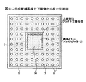
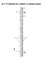
まず、本発明の第1実施例による半導体装置に用いられる配線基板について、図4、図5及び図6を参照しながら説明する。図4は本発明の第1実施例による半導体装置の断面図である。図5は本発明の第1実施例による半導体装置に用いられる配線基板断面図である。図6は図5に示す配線基板を下面側から見た平面図である。図4、図5及び図6において、図1に示す構成部品と同等な部品には同じ符号を付し、その説明は省略する。
【0020】
本発明の第1実施例による半導体装置30において、図4に示すように、配線基板31上に半導体素子32がフリップチップ実装されている。配線基板31と半導体素子32との間にはアンダーフィル材33が充填され、半導体素子32は配線基板上で封止樹脂34により封止される。配線基板31の下面には外部接続端子としてハンダボール35が設けられる。半導体装置30は、いわゆるファンアウトタイプの半導体装置であり、配線基板31中央部分に半導体素子32が搭載され、外部接続端子としてのハンダボール35は半導体素子32が搭載される領域の周囲の領域で、半導体素子32とは反対側に設けられる。
【0021】
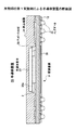
図5を参照すると、配線基板31は、図1に示す配線基板1と同様の両面配線基板であり、基板コア材2の上面2aにボンディングパッド3が形成され、下面2bにランド5が形成される。
【0022】
ここで、本実施例における配線基板31は、上面3aのボンディングパッド3が配列された領域に対応して、基板コア材2の下面2bに形成されたバックアップパターン36(パターン部材)を有する。バックアップパターン36は、基板コア材2の下面2bに設けられる導体パターンにより形成されるため、ランド5や下部配線(図5には示されていない)が図と同じ工程で形成され、同じ厚みを有している。ただし、バックアップパターン36は、下部配線やランド5からは分離されて孤立したパターンであることが好ましい。
【0023】
バックアップパターン36はボンディングパッド3が設けられる上面2aとは反対側の下面2bに形成され、図6に示すように、ボンディングパッド3が設けられた領域を包含するような大きさである。すなわち、バックアップパターン36は全てのボンディングパッド3の下側に延在する。また、バックアップパターン36は、導体パターンの露出部分以外を覆うためのソルダレジスト7により覆われる。したがって、配線基板31が図3に示すようなボンディングステージ20上に載置されたときに、ボンディングパッド3の下方における基板コア材2とボンディングステージ20との間には隙間が形成されることはない。
【0024】
このように、基板コア材2とボンディングステージ20との間に隙間が形成されないので、超音波フリップチップボンディングの際に、半導体素子32のバンプ32a(突起電極)がボンディングパッド3に押圧されても、配線基板31がたわむことはない。したがって、超音波振動エネルギの基板への吸収・拡散が減少し、良好な超音波接合を行うことができる。これにより、半導体装置の組み立て時の歩留まりが向上し、接合強度の改善による半導体装置の信頼性が向上する。
【0025】
また、バックアップパターン36は基板コア材2の比較的大きな面積を覆うため、配線基板31の剛性を増大させる効果がある。これにより、配線基板31の反りや変形を抑制し、半導体装置の信頼性向上に寄与する。更に、バックアップパターン36は金属であるため熱伝導性に優れており、且つ半導体素子32の真下に位置するため、半導体装置の放熱性が向上する。
【0026】
次に上述の配線基板31のいくつかの変形例について説明する。
【0027】
図7は配線基板31の第1の変形例である配線基板31Aの断面図であり、図8は図7に示す配線基板31Aを下面側から見た平面図である。図7及び図8において、図5及び図6に示す構成部品と同等な部品には同じ符号を付し、その説明は省略する。
【0028】
配線基板31Aは、図5に示す配線基板31と基本的に同じ構成を有するが、バックアップパターンの厚みが異なる。すなわち、配線基板31Aに設けられたバックアップパターン36Aは、下部配線やランドを形成する導体パターンより厚い部材により形成されており、ソルダレジスト7により覆われずに露出している。バックアップパターン36Aが厚くなったことにより、配線基板31Aの剛性は配線基板31より向上する。また、バックアップパターン36Aが露出していることにより、放熱性はより向上する。
【0029】
図9は図7に示す配線基板31Aを用いた半導体装置の変形例を示す断面図である。図9に示す半導体装置40は、配線基板31Aに半導体素子32を超音波フリップチップボンディングにより搭載し、その上に更に半導体素子41を積層している。半導体素子41は背面を半導体素子32の背面に対向した状態で、接着材42により半導体素子32に固定される。そして、半導体素子41はボンディングワイヤ43により、配線基板31Aの上面に形成されたボンンディングパッド44に接続される。半導体素子32、半導体素子41及びボンディングパッド43は、封止樹脂45により封止される。
【0030】
半導体装置40は配線基板31Aを用いているため、バックアップパターン36Aに関する上述の利点を有し、且つ、半導体素子42が積層されているため、半導体素子の実装密度が向上する等の利点も有する。なお、配線基板30Aを用いて図9のような積層構造の半導体装置を形成することとしてもよい。
【0031】
図10は配線基板31の第2の変形例である配線基板31Bの断面図であり、図11は図10に示す配線基板31Bを下面側から見た平面図である。また、図12は図10に示す配線基板31Bを用いた半導体装置の断面図である。図10、図11及び図12において、図5及び図6に示す構成部品と同等な部品には同じ符号を付し、その説明は省略する。
【0032】
図10に示す配線基板31Bは、図12に示すようないわゆるファンインタイプの半導体装置48に用いる配線基板として形成されたものである。したがって、半導体素子32の搭載領域は、配線基板31Bの全体とほぼ等しくなっており、配線基板31Bの下面の中央部分にランド5が形成される。そして、配線基板31Bの上面の周辺部分にボンディングパッド3が配置される。
【0033】
半導体装置48は、ボンディングパッド3の下側にバックアップパターン36Bを有しているため、図4に示す半導体装置と同様の利点を有する。また、半導体装置48は、いわゆるチップサイズ/スケールパッケージ(CSP)として構成れる。また、搭載される半導体素子32と配線基板31Bとはほぼ等しいサイズであるため、図4に示す半導体装置30のように封止樹脂34により封止する必要はなく、その分の製造工程が不要となり製造コストを低減することができる。なお、半導体装置48においても、バックアップパターン36Bの厚みを厚くして、図9に示すバックアップパターン36Aと同様の効果を得ることができる。
【0034】
図13は配線基板31の第3の変形例である配線基板31Cの断面図であり、図14は図13に示す配線基板31Cを下面側から見た平面図である。図13及び図14において、図5及び図6に示す構成部品と同等な部品には同じ符号を付し、その説明は省略する。
【0035】
図13に示す配線基板31Cは、搭載される半導体素子の電極配列に合わせて分割されたバックアップパターン36Cを有する。すなわち、搭載される半導体素子の電極は対向する2辺に沿って配列されたものであり、これに対応してバックアップパターンも2つのバックアップパターン36Cに分割される。バックアップパターン36Cの間に、図14に示すように、下部回線6を配置することができる。
【0036】
図15は配線基板31の第4の変形例である配線基板31Dの断面図であり、図16は図15に示す配線基板31Dを下面側から見た平面図である。また、図17は図15に示す配線基板31Dを用いた半導体装置の断面図である。図15、図16及び図17において、図5及び図6に示す構成部品と同等な部品には同じ符号を付し、その説明は省略する。
【0037】
図15に示す配線基板31Dは、接地端子に接続されたバックアップパターン36Dを有する。ランド5のうち、バックアップパターンに近接したランド5aが接地端子とされ、バックアップパターン36Dは図16に示すように接地端子であるランド5aに接続された形状に形成される。
【0038】
このようなバックアップパターン36Dにより、図5に示すバックアップパターン36と同様な効果を得ることができ、加えて半導体素子のシールド効果を得ることができる。
【0039】
図17は図15に示す配線基板31Dを用いた半導体装置50の断面図である。半導体装置50は、半導体素子32を配線基板31Dに超音波フリップチップボンディングして形成し、さらに、メタルキャップ51を配線基板31Dに取り付けたものである。メタルキャップ51は金属等の導電性材料で形成されており、配線基板31D上の半導体素子32を覆うような箱型形状を有する。メタルキャップ51の端部は、導電性接着材52により配線基板31Dの上面に形成された接地端子53に接続され固体される。
【0040】
したがって、半導体装置50において、半導体素子32は接地電位とされたメタルキャップ51と同じく接地電位とされた配線基板31Dとによりほぼ覆われた状態となる。これにより、半導体素子32のシールド効果が得られ、半導体装置50の電気的特性が向上する。
【0041】
次に、本発明の第2実施例による半導体装置について、図18、図19及び図20を参照しながら説明する。図18は本発明の第2実施例による半導体装置の断面図である。図19は本発明の第2実施例による半導体装置に用いられる配線基板の断面図であり、図20は図19に示す配線基板を下面側から見た平面図である。図18、図19及び図20において、図2に示す構成部品と同等な部品には同じ符号を付す。
【0042】
本発明の第2実施例による半導体装置60は、片面配線基板61を用いて形成されたファンアウトタイプの半導体装置である。配線基板61は、基板コア材12の片面だけに導体パターンが形成されている。導体パターンにより、ボンディングパッド13と、配線14と、外部接続端子を設けるためのランド15とが形成される。半導体素子32の電極(バンプ)32aは、ボンディングパッド13に対して超音波フリップチップボンディングされる。半導体素子32と配線基板61との間にはアンダーフィル材62が充填され、半導体素子32は配線基板61に対して固定される。
【0043】
ランド15の下には、基板コア材12を貫通して裏面まで延在する貫通孔16が形成されており、貫通孔16を介して外部接続端子としてハンダボール63がランド15に接続される。基板コア材12は、FR−4材やBTレジンのような有機材料を用いて形成される。
【0044】
本実施例における配線基板61では、上述の第1実施例と同様に、基板コア材12の上面12aにボンディングパッド13が形成され、下面12bにバックアップパターン64が設けられる。配線基板61は片面配線基板であり、基板コア材12の下面12bには配線等を形成するための導体パターンは設けられない。しかし、本実施例では超音波フリップチップボンディングの信頼性を向上させるために、例えば銅箔等よりなるバックアップパターン64を基板コア材12の下面12bに貼り付けている。
【0045】
配線基板61を図3に示すボンディングステージ20に載置した場合、バックアップパターン64がボンディングステージ20の載置面に接触し、基板コア材12とボンディングステージ20との間に隙間が形成されないので、超音波フリップチップボンディングの際に、半導体素子32のバンプ32aがボンディングパッド13に押圧されても、配線基板61がたわむことはない。したがって、超音波振動エネルギの基板への吸収・拡散が減少し、良好な超音波接合を行うことができる。これにより、半導体装置の組み立て時の歩留まりが向上し、接合強度の改善による半導体装置の信頼性が向上する。
【0046】
また、バックアップパターン64は基板コア材12の比較的大きな面積を覆うため、配線基板61の剛性を増大させる効果がある。これにより、配線基板61の反りや変形を抑制し、半導体装置の信頼性向上に寄与する。更に、バックアップパターン64は金属であるため熱伝導性に優れており、且つ半導体素子32の真下に位置するため、半導体装置の放熱性が向上する。
【0047】
図21は図19に示す配線基板61の変形例である配線基板61Aの断面図であり、図22は図21に示す配線基板61Aを下面から見た平面図である。また、図23は図21に示す配線基板61Aを用いた半導体装置の断面図である。図21、図22及び図23において、図18及び図19に示す構成部品と同等の部品には同じ符号を付し、その説明は省略する。
【0048】
図21に示す配線基板61Aは、図23に示すようないわゆるファンインタイプの半導体装置70に用いる配線基板として形成されたものである。したがって、半導体素子32の搭載領域は、配線基板61Bの全体とほぼ等しくなっており、配線基板61Bの上面の中央部分にランド15が形成される。そして、配線基板61Bの上面の周辺部分にボンディングパッド13が配置される。
【0049】
半導体装置70は、ボンディングパッド13の下側にバックアップパターン61Aを有しているため、図18に示す半導体装置60と同様の利点を有する。また、半導体装置70は、いわゆるチップサイズ/スケールパッケージ(CSP)として構成される。
【0050】
次に、上述の各実施例において、半導体素子を配線基板に超音波フリップチップボンディングにより配線基板に搭載する工程について、図4に示す本発明の第1実施例による半導体装置30を例にとって説明する。図24は図4に示す配線基板31に対して半導体素子32を超音波フリップチップボンディングする工程を説明するための図である。
【0051】
まず、図24(a)に示すように、バックアップパターン36がボンディングステージ20の平坦な載置面に対向した状態で配線基板31をボンディングステージ20上に載置し、真空吸引チャック等で固定する。配線基板31の固定を確実にするために、配線基板31の外周をクランプ治具21により固定する。一方、搭載される半導体素子32の背面をボンディングツール23に固定した状態で、バンプ32aと配線基板31のボンディングパッド3との位置合わせを行う。
【0052】
位置合わせが完了すると、図24(b)に示すように、半導体素子32のバンプ32aを配線基板31のボンディングパッド3に押圧する。この状態で、ボンディングツール23から半導体素子32に対して超音波振動を印加する。これにより、バンプ32aが超音波振動し、バンプ32aはボンディングパッド3に超音波接合される。
【0053】
上述の工程では、バックアップパターン36があるために、配線基板31とボンディングステージ20との間に隙間が形成されないので、超音波フリップチップボンディングの際に、半導体素子32のバンプ32aがボンディングパッド3に押圧されても、配線基板31がたわむことはない。したがって、超音波振動エネルギの基板への吸収・拡散が減少し、良好な超音波接合を行うことができる。これにより、半導体装置の組み立て時の歩留まりが向上し、接合強度の改善による半導体装置の信頼性が向上する。
【0054】
ここで、配線基板にバックアップパターンが形成されていない場合には、図25(a)に示すように、ボンディングステージ20にバックアップ治具80を配置することにより、バックアップパターンと同様の効果を得ることができる。すなわち、ボンディングステージ20の載置面の中央部分にバックアップ治具80を載置し、その上に配線基板31を載置して固定する。そして、半導体素子32を超音波フリップチップボンディングにより配線基板31に搭載する。
【0055】
バックアップ治具80の厚みは、配線基板31とボンディングステージの載置面との間に形成される隙間に応じて予め決められた寸法、すなわち、配線基板31が載置された際に配線基板31とボンディングステージ20との間に隙間が形成されないような寸法とする。バックアップ治具80の位置を決めて横方向の移動を防止するために、ボンディングステージ20の載置面に凹部を形成しておくことが好ましい。
【0056】
上述の如く、本明細書は以下の発明を開示する。
【0057】
(付記1) 突起電極を有する半導体素子と、
上面と該上面の反対側の下面とを有する基板コア材を有し、該半導体素子が該上面側にフリップチップ実装された配線基板と、
該基板コア材の該上面に形成され、前記半導体素子の前記突起電極が接合されるボンディングパッドと、
前記基板コア材の前記下面に形成され、該ボンディングパッドが設けられた位置に対応した位置に配置され、全てのボンディングパッドの真下に延在するように形成されたパターン部材と
を有することを特徴とする半導体装置。
(付記2) 付記1記載の半導体装置であって、
前記基板コア材の前記下面に形成され、外部接続端子が形成されるランドを更に有し、
前記パターン部材と該ランドとは同じ導電材料により形成された部材であることを特徴とする半導体装置。
(付記3) 付記2記載の半導体装置であって、
前記パターン部材の厚みは前記ランドの厚みに等しいことを特徴とする半導体装置。
【0058】
(付記4) 付記3記載の半導体装置であって、
前記ランドは接地電位とされたランドを含んでおり、前記パターン部材は該接地電位とされたランドに接続されていることを特徴とする半導体装置。
【0059】
(付記5) 付記4記載の半導体装置であって、
導電材料からなる箱状部材が前記半導体素子を覆うように前記コア基板の前記上面側に設けられ、箱状部材は前記上面上の接地端子に接続されていることを特徴とする半導体装置。
【0060】
(付記6) 付記1乃至5のうちいずれか一項記載の半導体装置であって、
前記基板パターン部材は複数に分割されており、分割されたパターン部材の間に配線パターンが配置されていることを特徴とする半導体装置。
【0061】
(付記7) 付記1記載の半導体装置であって、
前記パターン部材の厚みは前記ランドの厚みより大きいことを特徴とする半導体装置。
【0062】
(付記8) 付記1記載の半導体装置であって、
前記基板コア材の前記上面にランドが形成され、該ランドの下に前記基板コア材を貫通して前記下面まで延在する貫通孔が設けられ、該貫通孔を介して前記ランドに接続された外部接続端子が前記下面側に設けられたことを特徴とする半導体装置。
(付記9) 付記8記載の半導体装置であって、
前記パターン部材は金属材料よりなる板状部材であることを特徴とする半導体装置。
(付記10) 付記1乃至9のうちいずれか一項記載の半導体装置であって、
前記基板コア材は有機材料よりなることを特徴とする半導体装置。
【0063】
(付記11) 半導体素子がフリップチップ実装される配線基板であって、
上面と該上面の反対側の下面とを有する基板コア材と、
該基板コア材の該上面に形成され、前記半導体素子の突起電極が接合されるボンディングパッドと、
前記基板コア材の前記下面に形成され、該ボンディングパッドが設けられた位置に対応した位置に配置され、全てのボンディングパッドの真下に延在するように形成されたパターン部材と
を有することを特徴とする配線基板。
(付記12) 付記11記載の配線基板であって、
前記基板コア材の前記下面に形成され、外部接続端子が形成されるランドを更に有し、
前記パターン部材と該ランドとは同じ導電材料により形成された部材であることを特徴とする配線基板。
【0064】
(付記13) 付記11記載の配線基板であって、
前記パターン部材の厚みは前記ランドの厚みより大きいことを特徴とする配線基板。
【0065】
(付記14) 付記11記載の配線基板であって、
前記基板コア材の前記上面にランドが形成され、該ランドの下に前記基板コア材を貫通して前記下面まで延在する貫通孔が設けられ、該貫通孔を介して前記ランドに接続された外部接続端子が前記下面側に設けられたことを特徴とする配線基板。
【0066】
(付記15) 付記14記載の配線基板であって、
前記パターン部材は金属材料よりなる板状部材であることを特徴とする配線基板。
【0067】
(付記16) 付記11乃至15のうちいずれか一項記載の配線基板であって、
前記基板コア材は有機材料よりなることを特徴とする配線基板。
【0068】
(付記17) 超音波フリップチップボンディングを用いた半導体装置の製造方法であって、
上面に形成されたボンディングパッドに対応した位置の下面にパターン部材を有する配線基板をボンディングステージ上に載置して固定し、
半導体素子の突起電極を超音波フリップチップボンディングにより前記配線基板のボンディングパッドに接合する
ことを特徴とする半導体装置の製造方法。
【0069】
(付記18) 超音波フリップチップボンディングを用いた半導体装置の製造方法であって、
載置される配線基板のボンディングパッド位置に対応したボンディングステージ上の位置にバックアップ治具を配置し、
該バックアップ治具を介して配線基板を前記ボンディングステージ上に載置して固定し、
半導体素子の突起電極を超音波フリップチップボンディングにより前記配線基板のボンディングパッドに接合する
ことを特徴とする半導体装置の製造方法。
【発明の効果】
上述の如く本発明によれば、バックアップパターンが設けられたことによりボンディングステージの載置面と配線基板との間に隙間が形成されないので、超音波フリップチップボンディングの際に配線基板がたわむことなく、良好なボンディングを達成することができる。これにより、半導体装置の組み立て時の歩留まりが向上し、接合強度の改善による半導体装置の信頼性が向上する。
【図面の簡単な説明】
【図1】従来の両面配線基板の断面図である。
【図2】従来の片面配線基板の断面図である。
【図3】図1に示す配線基板に半導体素子を超音波フリップチップボンディングする工程を説明するための図である。
【図4】本発明の第1実施例による半導体装置の断面図である。
【図5】本発明の第1実施例による半導体装置に用いられる配線基板の断面図である。
【図6】図5に示す配線基板を下面側から見た平面図である。
【図7】図5に示す配線基板の第1の変形例である配線基板の断面図である。
【図8】図7に示す配線基板を下面側から見た平面図である。
【図9】図7に示す配線基板を用いた半導体装置の変形例を示す断面図である。
【図10】図5に示す配線基板の第2の変形例である配線基板の断面図である。
【図11】図10に示す配線基板を下面側から見た平面図である。
【図12】図10に示す配線基板を用いた半導体装置の断面図である。
【図13】図5に示す配線基板の第3の変形例である配線基板の断面図である。
【図14】図13に示す配線基板を下面側から見た平面図である。
【図15】図5に示す配線基板の第4の変形例である配線基板の断面図である。
【図16】図15に示す配線基板を下面側から見た平面図である。
【図17】図15に示す配線基板を用いた半導体装置の断面図である。
【図18】本発明の第2実施例による半導体装置の断面図である。
【図19】本発明の第2実施例による半導体装置に用いられる配線基板の断面図である。
【図20】図19に示す配線基板を下面側から見た平面図である。
【図21】図19に示す配線基板の変形例である配線基板の断面図である。
【図22】図21に示す配線基板を下面側から見た平面図である。
【図23】図23は図21に示す配線基板を用いた半導体装置の断面図である。
【図24】図4に示す配線基板に対して半導体素子を超音波フリップチップボンディングする工程を説明するための図である。
【図25】超音波フリップチップボンディングの他の方法を説明するための図である。
【符号の説明】
2,12 基板コア材
3,13 ボンディングパッド
4 上部配線
5,15 ランド
5a,35a 接地端子
7 ソルダレジスト
14 配線
16 貫通孔
30,40,48,50,60,70 半導体装置
31,31A,31B,31C,31D,61,61A 配線基板
32,41 半導体素子
32a バンプ
33 アンダーフィル材
34,45 封止樹脂
35 ハンダボール
36,36A,36B,36C,36D,64,64A バックアップパターン
43 ボンディングワイヤ
44 端子
51 メタルキャップ
52 導電性接着材[0001]
TECHNICAL FIELD OF THE INVENTION
The present invention relates to a semiconductor device, and more particularly to a semiconductor device formed by connecting a semiconductor element to a wiring board by flip chip bonding using ultrasonic waves.
[0002]
[Prior art]
In order to provide an external connection terminal as a semiconductor device, wiring is routed using a wiring board called a so-called interposer, and semiconductor packages in which external connection terminals are efficiently arranged are increasing. In a process of manufacturing such a semiconductor package, when mounting a semiconductor element on a wiring board, a so-called ultrasonic flip chip bonding for joining a bump of the semiconductor element to an electrode of the wiring board using ultrasonic waves is often used. .
[0003]
2. Description of the Related Art In recent years, the size of a semiconductor device has been increasing with the advancement of functions of the semiconductor device, and several large-sized ultrasonic vibration tools for flip chip bonding corresponding to large semiconductor devices have been developed. As a result, large semiconductor elements have also been mounted by ultrasonic flip chip bonding.
[0004]
A ceramic substrate, a resin tape substrate, an organic substrate, or the like is used as a wiring substrate on which a semiconductor element is flip-chip mounted. Among them, for example, an organic substrate such as a glass epoxy substrate is superior to other substrates in terms of handling and cost, and is often used.
[0005]
FIG. 1 is a sectional view of a conventional double-sided wiring board. The
[0006]
FIG. 2 is a sectional view of a conventional single-sided wiring type wiring board. The
[0007]
[Problems to be solved by the invention]
When the semiconductor element is flip-chip mounted on the
[0008]
FIG. 3 is a view for explaining a step of ultrasonic flip chip bonding of the semiconductor element 10 to the
[0009]
When the alignment is completed, the bumps of the
[0010]
Here, since the land 5 and the wiring portion are formed on the lower surface side of the
[0011]
Further, even when the single-
[0012]
The present invention has been made in view of the above points, and an object of the present invention is to provide a semiconductor device in which a semiconductor element is reliably ultrasonically flip-chip bonded to a wiring substrate and a wiring substrate used in such a semiconductor device. Aim.
[0013]
[Means for Solving the Problems]
According to the present invention, there is provided a semiconductor device having a protruding electrode, a substrate core material having an upper surface and a lower surface opposite to the upper surface, wherein the semiconductor device is flipped to the upper surface side. A wiring board mounted with a chip, a bonding pad formed on the upper surface of the substrate core material and joined to the protruding electrode of the semiconductor element, and a bonding pad formed on the lower surface of the substrate core material. And a pattern member formed at a position corresponding to the set position and extending immediately below all the bonding pads.
[0014]
According to the invention described above, since no gap is formed between the mounting surface of the bonding stage and the wiring board due to the provision of the pattern member, the wiring board does not bend during ultrasonic flip chip bonding, which is favorable. Bonding can be achieved.
[0015]
The semiconductor device according to the above-described invention further includes a land formed on the lower surface of the substrate core material and on which an external connection terminal is formed, wherein the pattern member and the land are members formed of the same conductive material. It may be good. That is, the pattern member and the land can be formed by patterning one conductive member.
[0016]
Further, a land is formed on the upper surface of the substrate core material, and a through hole is provided below the land so as to penetrate the substrate core material and extend to the lower surface, and is connected to the land via the through hole. The connected external connection terminal may be provided on the lower surface side.
[0017]
Further, a through-hole extending through the substrate core material and extending to the lower surface is provided under the land, and an external connection terminal connected to the land via the through-hole is provided on the lower surface side. Is also good. Preferably, the pattern member is a plate-like member made of a metal material.
[0018]
Further, according to the present invention, a wiring board on which the semiconductor element is flip-chip mounted, a substrate core material having an upper surface and a lower surface opposite to the upper surface, and formed on the upper surface of the substrate core material, A bonding pad to which the protruding electrode of the semiconductor element is bonded; and a bonding pad formed on the lower surface of the substrate core material, disposed at a position corresponding to a position where the bonding pad is provided, and extending directly below all the bonding pads. And a pattern member formed as described above. With such a wiring board, the same effect as that of the above-described semiconductor device can be obtained.
BEST MODE FOR CARRYING OUT THE INVENTION
Next, embodiments of the present invention will be described with reference to the drawings.
[0019]
First, a wiring board used in a semiconductor device according to a first embodiment of the present invention will be described with reference to FIG. 4, FIG. 5, and FIG. FIG. 4 is a sectional view of a semiconductor device according to a first embodiment of the present invention. FIG. 5 is a sectional view of a wiring board used in the semiconductor device according to the first embodiment of the present invention. FIG. 6 is a plan view of the wiring board shown in FIG. 5 as viewed from the lower surface side. 4, 5, and 6, parts that are the same as the parts shown in FIG. 1 are given the same reference numerals, and descriptions thereof will be omitted.
[0020]
In the semiconductor device 30 according to the first embodiment of the present invention, a
[0021]
Referring to FIG. 5, a
[0022]
Here, the
[0023]
The
[0024]
As described above, since no gap is formed between the substrate core material 2 and the
[0025]
Further, since the
[0026]
Next, some modifications of the above-described
[0027]
FIG. 7 is a sectional view of a
[0028]
[0029]
FIG. 9 is a cross-sectional view showing a modification of the semiconductor device using the
[0030]
Since the semiconductor device 40 uses the
[0031]
FIG. 10 is a sectional view of a
[0032]
The
[0033]
Since the semiconductor device 48 has the
[0034]
FIG. 13 is a sectional view of a
[0035]
The
[0036]
FIG. 15 is a sectional view of a
[0037]
The
[0038]
With such a
[0039]
FIG. 17 is a cross-sectional view of a semiconductor device 50 using the
[0040]
Therefore, in the semiconductor device 50, the
[0041]
Next, a semiconductor device according to a second embodiment of the present invention will be described with reference to FIGS. FIG. 18 is a sectional view of a semiconductor device according to a second embodiment of the present invention. FIG. 19 is a sectional view of a wiring board used in the semiconductor device according to the second embodiment of the present invention, and FIG. 20 is a plan view of the wiring board shown in FIG. 18, 19, and 20, parts that are the same as the parts shown in FIG. 2 are given the same reference numerals.
[0042]
The semiconductor device 60 according to the second embodiment of the present invention is a fan-out type semiconductor device formed using a single-
[0043]
A through
[0044]
In the
[0045]
When the
[0046]
Further, since the
[0047]
FIG. 21 is a sectional view of a wiring board 61A which is a modification of the
[0048]
A wiring board 61A shown in FIG. 21 is formed as a wiring board used for a so-called fan-in
[0049]
Since the
[0050]
Next, in each of the above-described embodiments, a step of mounting a semiconductor element on a wiring board by ultrasonic flip chip bonding will be described with reference to the semiconductor device 30 according to the first embodiment of the present invention shown in FIG. 4 as an example. . FIG. 24 is a view for explaining a step of performing ultrasonic flip chip bonding of the
[0051]
First, as shown in FIG. 24A, the
[0052]
When the alignment is completed, the
[0053]
In the above-described process, since there is no gap between the
[0054]
Here, when the backup pattern is not formed on the wiring board, the same effect as the backup pattern can be obtained by disposing the
[0055]
The thickness of the
[0056]
As described above, the present specification discloses the following inventions.
[0057]
(Supplementary Note 1) A semiconductor element having a protruding electrode,
A wiring board having a substrate core material having an upper surface and a lower surface opposite to the upper surface, wherein the semiconductor element is flip-chip mounted on the upper surface side;
A bonding pad formed on the upper surface of the substrate core material and joined to the protruding electrode of the semiconductor element;
A pattern member formed on the lower surface of the substrate core material, disposed at a position corresponding to a position where the bonding pad is provided, and formed to extend directly below all the bonding pads;
A semiconductor device comprising:
(Supplementary Note 2) The semiconductor device according to
Further comprising a land formed on the lower surface of the substrate core material, on which an external connection terminal is formed;
The semiconductor device, wherein the pattern member and the land are members formed of the same conductive material.
(Supplementary Note 3) The semiconductor device according to Supplementary Note 2, wherein
The semiconductor device according to
[0058]
(Supplementary Note 4) The semiconductor device according to
The semiconductor device according to
[0059]
(Supplementary Note 5) The semiconductor device according to Supplementary Note 4, wherein
A semiconductor device, wherein a box-shaped member made of a conductive material is provided on the upper surface side of the core substrate so as to cover the semiconductor element, and the box-shaped member is connected to a ground terminal on the upper surface.
[0060]
(Supplementary Note 6) The semiconductor device according to any one of
The semiconductor device according to
[0061]
(Supplementary Note 7) The semiconductor device according to
The semiconductor device according to
[0062]
(Supplementary Note 8) The semiconductor device according to
A land was formed on the upper surface of the substrate core material, a through hole extending through the substrate core material to the lower surface was provided below the land, and connected to the land via the through hole. A semiconductor device, wherein an external connection terminal is provided on the lower surface side.
(Supplementary Note 9) The semiconductor device according to
The semiconductor device according to
(Supplementary Note 10) The semiconductor device according to any one of
A semiconductor device, wherein the substrate core material is made of an organic material.
[0063]
(Supplementary Note 11) A wiring board on which the semiconductor element is flip-chip mounted,
A substrate core material having an upper surface and a lower surface opposite the upper surface,
A bonding pad formed on the upper surface of the substrate core material, to which a bump electrode of the semiconductor element is bonded;
A pattern member formed on the lower surface of the substrate core material, disposed at a position corresponding to a position where the bonding pad is provided, and formed to extend directly below all the bonding pads;
A wiring substrate comprising:
(Supplementary Note 12) The wiring board according to
Further comprising a land formed on the lower surface of the substrate core material, on which an external connection terminal is formed;
The wiring board, wherein the pattern member and the land are members formed of the same conductive material.
[0064]
(Supplementary Note 13) The wiring board according to
A wiring board, wherein the thickness of the pattern member is larger than the thickness of the land.
[0065]
(Supplementary Note 14) The wiring board according to
A land was formed on the upper surface of the substrate core material, a through hole extending through the substrate core material to the lower surface was provided below the land, and connected to the land via the through hole. A wiring board, wherein an external connection terminal is provided on the lower surface side.
[0066]
(Supplementary Note 15) The wiring board according to supplementary note 14, wherein
The wiring board, wherein the pattern member is a plate-shaped member made of a metal material.
[0067]
(Supplementary Note 16) The wiring board according to any one of
A wiring substrate, wherein the substrate core material is made of an organic material.
[0068]
(Supplementary Note 17) A method of manufacturing a semiconductor device using ultrasonic flip chip bonding,
A wiring board having a pattern member on the lower surface at a position corresponding to the bonding pad formed on the upper surface is placed on a bonding stage and fixed,
A protruding electrode of a semiconductor element is bonded to a bonding pad of the wiring substrate by ultrasonic flip chip bonding
A method for manufacturing a semiconductor device, comprising:
[0069]
(Supplementary Note 18) A method of manufacturing a semiconductor device using ultrasonic flip chip bonding,
Arrange the backup jig at a position on the bonding stage corresponding to the bonding pad position of the wiring board to be mounted,
Placing the wiring board on the bonding stage via the backup jig and fixing it,
A protruding electrode of a semiconductor element is bonded to a bonding pad of the wiring substrate by ultrasonic flip chip bonding
A method for manufacturing a semiconductor device, comprising:
【The invention's effect】
As described above, according to the present invention, since a gap is not formed between the mounting surface of the bonding stage and the wiring board due to the provision of the backup pattern, the wiring board does not bend during ultrasonic flip chip bonding. , Good bonding can be achieved. Thereby, the yield at the time of assembling the semiconductor device is improved, and the reliability of the semiconductor device is improved by improving the bonding strength.
[Brief description of the drawings]
FIG. 1 is a cross-sectional view of a conventional double-sided wiring board.
FIG. 2 is a sectional view of a conventional single-sided wiring board.
FIG. 3 is a view for explaining a step of performing ultrasonic flip-chip bonding of a semiconductor element to the wiring board shown in FIG. 1;
FIG. 4 is a sectional view of the semiconductor device according to the first embodiment of the present invention;
FIG. 5 is a sectional view of a wiring board used in the semiconductor device according to the first embodiment of the present invention.
FIG. 6 is a plan view of the wiring board shown in FIG. 5 as viewed from a lower surface side.
FIG. 7 is a cross-sectional view of a wiring board which is a first modification of the wiring board shown in FIG.
8 is a plan view of the wiring board shown in FIG. 7 as viewed from the lower surface side.
9 is a cross-sectional view showing a modification of the semiconductor device using the wiring board shown in FIG.
FIG. 10 is a sectional view of a wiring board which is a second modification of the wiring board shown in FIG.
11 is a plan view of the wiring board shown in FIG. 10 as viewed from the lower surface side.
12 is a cross-sectional view of a semiconductor device using the wiring board shown in FIG.
FIG. 13 is a sectional view of a wiring board which is a third modification of the wiring board shown in FIG. 5;
14 is a plan view of the wiring board shown in FIG. 13 as viewed from a lower surface side.
FIG. 15 is a sectional view of a wiring board which is a fourth modification of the wiring board shown in FIG. 5;
FIG. 16 is a plan view of the wiring board shown in FIG. 15 as viewed from the lower surface side.
17 is a sectional view of a semiconductor device using the wiring board shown in FIG.
FIG. 18 is a sectional view of a semiconductor device according to a second embodiment of the present invention.
FIG. 19 is a sectional view of a wiring board used in a semiconductor device according to a second embodiment of the present invention.
20 is a plan view of the wiring board shown in FIG. 19 as viewed from the lower surface side.
21 is a sectional view of a wiring board which is a modification of the wiring board shown in FIG.
FIG. 22 is a plan view of the wiring board shown in FIG. 21 as viewed from the lower surface side.
FIG. 23 is a sectional view of a semiconductor device using the wiring board shown in FIG. 21;
FIG. 24 is a view for explaining a step of performing ultrasonic flip chip bonding of the semiconductor element to the wiring board shown in FIG. 4;
FIG. 25 is a diagram for explaining another method of ultrasonic flip chip bonding.
[Explanation of symbols]
2,12 substrate core material
3,13 bonding pad
4 Top wiring
5,15 rand
5a, 35a Ground terminal
7 Solder resist
14 Wiring
16 Through hole
30, 40, 48, 50, 60, 70 semiconductor device
31, 31A, 31B, 31C, 31D, 61, 61A Wiring board
32,41 semiconductor device
32a bump
33 Underfill material
34, 45 sealing resin
35 Solder Ball
36,36A, 36B, 36C, 36D, 64,64A Backup pattern
43 Bonding wire
44 terminals
51 metal cap
52 conductive adhesive
Claims (5)
上面と該上面の反対側の下面とを有する基板コア材を有し、該半導体素子が該上面側にフリップチップ実装された配線基板と、
該基板コア材の該上面に形成され、前記半導体素子の前記突起電極が接合されるボンディングパッドと、
前記基板コア材の前記下面に形成され、該ボンディングパッドが設けられた位置に対応した位置に配置され、全てのボンディングパッドの真下に延在するように形成されたパターン部材と
を有することを特徴とする半導体装置。A semiconductor element having a protruding electrode;
A wiring board having a substrate core material having an upper surface and a lower surface opposite to the upper surface, wherein the semiconductor element is flip-chip mounted on the upper surface side;
A bonding pad formed on the upper surface of the substrate core material and joined to the protruding electrode of the semiconductor element;
A pattern member formed on the lower surface of the substrate core material, arranged at a position corresponding to a position where the bonding pad is provided, and formed to extend directly below all the bonding pads. Semiconductor device.
前記基板コア材の前記下面に形成され、外部接続端子が形成されるランドを更に有し、
前記パターン部材と該ランドとは同じ導電材料により形成された部材であることを特徴とする半導体装置。The semiconductor device according to claim 1,
Further comprising a land formed on the lower surface of the substrate core material, on which an external connection terminal is formed;
The semiconductor device, wherein the pattern member and the land are members formed of the same conductive material.
前記基板コア材の前記上面にランドが形成され、該ランドの下に前記基板コア材を貫通して前記下面まで延在する貫通孔が設けられ、該貫通孔を介して前記ランドに接続された外部接続端子が前記下面側に設けられたことを特徴とする半導体装置。The semiconductor device according to claim 1,
A land was formed on the upper surface of the substrate core material, a through hole extending through the substrate core material to the lower surface was provided below the land, and connected to the land via the through hole. A semiconductor device, wherein an external connection terminal is provided on the lower surface side.
前記パターン部材は金属材料よりなる板状部材であることを特徴とする半導体装置。The semiconductor device according to claim 1, wherein:
The semiconductor device according to claim 1, wherein the pattern member is a plate-shaped member made of a metal material.
上面と該上面の反対側の下面とを有する基板コア材と、
該基板コア材の該上面に形成され、前記半導体素子の突起電極が接合されるボンディングパッドと、
前記基板コア材の前記下面に形成され、該ボンディングパッドが設けられた位置に対応した位置に配置され、全てのボンディングパッドの真下に延在するように形成されたパターン部材と
を有することを特徴とする配線基板。A wiring board on which the semiconductor element is flip-chip mounted,
A substrate core material having an upper surface and a lower surface opposite the upper surface,
A bonding pad formed on the upper surface of the substrate core material, to which a bump electrode of the semiconductor element is bonded;
A pattern member formed on the lower surface of the substrate core material, arranged at a position corresponding to a position where the bonding pad is provided, and formed to extend directly below all the bonding pads. Wiring board.
Priority Applications (1)
| Application Number | Priority Date | Filing Date | Title |
|---|---|---|---|
| JP2002250934A JP2004095612A (en) | 2002-08-29 | 2002-08-29 | Semiconductor device and wiring board |
Applications Claiming Priority (1)
| Application Number | Priority Date | Filing Date | Title |
|---|---|---|---|
| JP2002250934A JP2004095612A (en) | 2002-08-29 | 2002-08-29 | Semiconductor device and wiring board |
Publications (2)
| Publication Number | Publication Date |
|---|---|
| JP2004095612A true JP2004095612A (en) | 2004-03-25 |
| JP2004095612A5 JP2004095612A5 (en) | 2005-11-04 |
Family
ID=32057639
Family Applications (1)
| Application Number | Title | Priority Date | Filing Date |
|---|---|---|---|
| JP2002250934A Pending JP2004095612A (en) | 2002-08-29 | 2002-08-29 | Semiconductor device and wiring board |
Country Status (1)
| Country | Link |
|---|---|
| JP (1) | JP2004095612A (en) |
Cited By (2)
| Publication number | Priority date | Publication date | Assignee | Title |
|---|---|---|---|---|
| JP2008135428A (en) * | 2006-11-27 | 2008-06-12 | Matsushita Electric Ind Co Ltd | Semiconductor device and electronic equipment using same |
| JP2020136624A (en) * | 2019-02-26 | 2020-08-31 | 新日本無線株式会社 | Semiconductor device |
-
2002
- 2002-08-29 JP JP2002250934A patent/JP2004095612A/en active Pending
Cited By (3)
| Publication number | Priority date | Publication date | Assignee | Title |
|---|---|---|---|---|
| JP2008135428A (en) * | 2006-11-27 | 2008-06-12 | Matsushita Electric Ind Co Ltd | Semiconductor device and electronic equipment using same |
| JP2020136624A (en) * | 2019-02-26 | 2020-08-31 | 新日本無線株式会社 | Semiconductor device |
| JP7260220B2 (en) | 2019-02-26 | 2023-04-18 | 日清紡マイクロデバイス株式会社 | semiconductor equipment |
Similar Documents
| Publication | Publication Date | Title |
|---|---|---|
| KR100537972B1 (en) | Chip scale ball grid array for integrated circuit package | |
| JP5017977B2 (en) | Semiconductor device and manufacturing method thereof | |
| TW494511B (en) | Semiconductor device and method of fabricating the same, circuit board, and electronic equipment | |
| TWI529878B (en) | Hybrid thermal interface material for ic packages with integrated heat spreader | |
| KR100532179B1 (en) | Chip scale ball grid array for integrated circuit package | |
| TWI343097B (en) | Packaging configurations for vertical electronic devices using conductive traces disposed on laminated board layers | |
| US8450853B2 (en) | Semiconductor device and a method of manufacturing the same, and an electronic device | |
| KR20010090379A (en) | Semiconductor package | |
| TW201436130A (en) | Thermally enhanced wiring board with built-in heat sink and build-up circuitry | |
| KR20020078931A (en) | Carrier frame for semiconductor package and semiconductor package using it and its manufacturing method | |
| JPH1174403A (en) | Semiconductor device | |
| JP3786103B2 (en) | SEMICONDUCTOR DEVICE, ELECTRONIC DEVICE, ELECTRONIC DEVICE, AND SEMICONDUCTOR DEVICE MANUFACTURING METHOD | |
| JP2000082722A (en) | Semiconductor device and its manufacture as well as circuit board and electronic apparatus | |
| JP2001077294A (en) | Semiconductor device | |
| JP4556671B2 (en) | Semiconductor package and flexible circuit board | |
| JP3695458B2 (en) | Semiconductor device, circuit board and electronic equipment | |
| JP2010073771A (en) | Mounting structure for semiconductor device | |
| JP2004128356A (en) | Semiconductor device | |
| JP2004095612A (en) | Semiconductor device and wiring board | |
| KR20120126365A (en) | Unit package and stack package having the same | |
| JP2004087936A (en) | Semiconductor device, manufacturing method thereof, and electronic appliance | |
| JP3670371B2 (en) | Semiconductor device and manufacturing method thereof | |
| JP3743811B2 (en) | Manufacturing method of semiconductor device | |
| JP2005044989A (en) | Semiconductor package and its manufacturing method | |
| JP2007150346A (en) | Semiconductor device and method of manufacturing same, circuit board, and electronic apparatus |
Legal Events
| Date | Code | Title | Description |
|---|---|---|---|
| A521 | Written amendment |
Effective date: 20050805 Free format text: JAPANESE INTERMEDIATE CODE: A523 |
|
| A621 | Written request for application examination |
Free format text: JAPANESE INTERMEDIATE CODE: A621 Effective date: 20050805 |
|
| A977 | Report on retrieval |
Effective date: 20060201 Free format text: JAPANESE INTERMEDIATE CODE: A971007 |
|
| A131 | Notification of reasons for refusal |
Free format text: JAPANESE INTERMEDIATE CODE: A131 Effective date: 20061003 |
|
| A02 | Decision of refusal |
Free format text: JAPANESE INTERMEDIATE CODE: A02 Effective date: 20070213 |