JP2004040799A - Wideband amplifier for bandwidth expansion - Google Patents
Wideband amplifier for bandwidth expansion Download PDFInfo
- Publication number
- JP2004040799A JP2004040799A JP2003191732A JP2003191732A JP2004040799A JP 2004040799 A JP2004040799 A JP 2004040799A JP 2003191732 A JP2003191732 A JP 2003191732A JP 2003191732 A JP2003191732 A JP 2003191732A JP 2004040799 A JP2004040799 A JP 2004040799A
- Authority
- JP
- Japan
- Prior art keywords
- amplifier
- bandwidth
- gain
- buffer
- inductor
- Prior art date
- Legal status (The legal status is an assumption and is not a legal conclusion. Google has not performed a legal analysis and makes no representation as to the accuracy of the status listed.)
- Pending
Links
- 230000001939 inductive effect Effects 0.000 claims abstract description 19
- 230000003139 buffering effect Effects 0.000 claims abstract description 11
- 230000001965 increasing effect Effects 0.000 claims description 7
- 238000013461 design Methods 0.000 claims description 4
- 239000004065 semiconductor Substances 0.000 claims description 4
- 230000003321 amplification Effects 0.000 description 13
- 238000003199 nucleic acid amplification method Methods 0.000 description 13
- 238000000034 method Methods 0.000 description 7
- 230000005540 biological transmission Effects 0.000 description 6
- 238000004891 communication Methods 0.000 description 5
- 238000010586 diagram Methods 0.000 description 4
- 238000004088 simulation Methods 0.000 description 3
- 238000005516 engineering process Methods 0.000 description 2
- 230000003287 optical effect Effects 0.000 description 2
- 238000012546 transfer Methods 0.000 description 2
- 239000003990 capacitor Substances 0.000 description 1
- 230000000694 effects Effects 0.000 description 1
- 238000012986 modification Methods 0.000 description 1
- 230000004048 modification Effects 0.000 description 1
- 239000013307 optical fiber Substances 0.000 description 1
- 230000003071 parasitic effect Effects 0.000 description 1
Images


Classifications
-
- H—ELECTRICITY
- H03—ELECTRONIC CIRCUITRY
- H03F—AMPLIFIERS
- H03F1/00—Details of amplifiers with only discharge tubes, only semiconductor devices or only unspecified devices as amplifying elements
- H03F1/42—Modifications of amplifiers to extend the bandwidth
-
- H—ELECTRICITY
- H03—ELECTRONIC CIRCUITRY
- H03F—AMPLIFIERS
- H03F1/00—Details of amplifiers with only discharge tubes, only semiconductor devices or only unspecified devices as amplifying elements
- H03F1/42—Modifications of amplifiers to extend the bandwidth
- H03F1/48—Modifications of amplifiers to extend the bandwidth of aperiodic amplifiers
-
- H—ELECTRICITY
- H03—ELECTRONIC CIRCUITRY
- H03F—AMPLIFIERS
- H03F3/00—Amplifiers with only discharge tubes or only semiconductor devices as amplifying elements
- H03F3/34—DC amplifiers in which all stages are DC-coupled
- H03F3/343—DC amplifiers in which all stages are DC-coupled with semiconductor devices only
- H03F3/3432—DC amplifiers in which all stages are DC-coupled with semiconductor devices only with bipolar transistors
-
- H—ELECTRICITY
- H03—ELECTRONIC CIRCUITRY
- H03F—AMPLIFIERS
- H03F2200/00—Indexing scheme relating to amplifiers
- H03F2200/36—Indexing scheme relating to amplifiers the amplifier comprising means for increasing the bandwidth
Landscapes
- Engineering & Computer Science (AREA)
- Power Engineering (AREA)
- Amplifiers (AREA)
Abstract
Description
【0001】
【発明の属する技術分野】
本発明は広帯域増幅装置に関し、更に詳しくは、インダクティブバッファを用いて帯域幅を拡張するための広帯域増幅装置に関する。
【0002】
【従来の技術】
最近、超高速データ通信技術、例えば、光ファイバを用いる光通信技術が急速に成長しており、これにより、データの伝送量に対する要求も高まっている。多くの量のデータを転送するためには、より広い帯域幅で作動する広帯域増幅器を実現することが必須である。このために、超高周波帯域で安定して作動することができる能動素子が開発される必要がある。しかし、このような新しい能動素子を開発するのに長い時間や高コストがかかるので、新しく開発された素子やそれ以外のものをどのように広帯域増幅器回路に設けるか、すなわち、新しく開発された素子が効率的に作動するように広帯域増幅器回路を設計する方法を改善することも重要である。
【0003】
通常、シャントインダクタ方式が広帯域増幅器回路を設計するのに用いられている。
【0004】
図1は、シャントインダクタ方式を採用する従来の広帯域増幅器100の概略的な回路図で、従来の広帯域増幅器100は、トランジスタTR101乃至TR104、多数個の抵抗及びインダクタL100を備える。3つのトランジスタTR101乃至TR103は、それぞれ、第1増幅段、バッファ段、及び第2増幅段を形成する。バッファ段TR102をバイアスするために設計されるトランジスタTR104は、特定の抵抗値を有する抵抗に代えることができる。また、それぞれの抵抗は、バイアス設計のための特定の抵抗値を有する。インダクタL100は、TR101のコレクタに接続されて、広帯域増幅器100の帯域幅が拡張できるようにする。
【0005】
上述のシャントインダクタ方式によると、インダクタL100とパッド(図示せず)の寄生コンデンサとの間に共振現象が発生する。共振現象は、帯域周波数が増加するにつれて従来の広帯域増幅器100の負荷端のインピーダンスを増加させ、高周波数帯域における利得を増加し、ついに帯域幅を増加する。
【0006】
しかし、シャントインダクタ方式は、利得増加及び帯域幅拡張と共に、増幅器の性能を劣化し得る相当な利得ピーキングを伴う。このような利得特性が図2に示されている。
【0007】
図2は、通常の増幅器及びシャントインダクタ方式を採用する従来の広帯域増幅器100の利得特性グラフを示し、グラフGaは通常の増幅器の利得特性を示し、グラフGbは従来の広帯域増幅器100の利得特性を示す。x軸は周波数Hzを示し、y軸は伝送インピーダンス利得dBΩを示す。
【0008】
約50dBΩの伝送インピーダンスにおいて、従来の広帯域増幅器は、8.4GHzの帯域幅を有する通常の増幅器に比較して、より大きい10.5GHzの有効帯域幅を有する。しかし、グラフからわかるように、これは2dBΩ以上の相当な利得ピーキングを有する。データが処理される有効帯域幅内におけるこのような相当な利得変化は、後に接続される制限増幅器の最大許容入力電圧を超過して、作動エラーを起すことがある。
【0009】
その故に、利得変化が殆どない、十分な帯域幅拡張を得るための帯域幅拡張方式が求められる。
【0010】
【発明が解決しようとする課題】
本発明は上記事情に鑑みてなされたものであり、その目的とするところは、利得変化が殆どない、帯域幅を拡張することができる増幅装置を提供することにある。
【0011】
【課題を解決するための手段】
上記目的を達成するために、本発明の実施の形態は、帯域幅を拡張するための広帯域増幅装置であって、入力信号を増幅するための第1及び第2増幅素子と、前記第1増幅素子と前記第2増幅素子との間に設けられ、出力信号の帯域幅を保持し、利得を増加し、バッファリングされた信号の一部を前記第1増幅素子に戻すことにより、前記第1増幅素子の出力信号をバッファリングするためのバッファリング素子と前記バッファリング素子に接続されており、帯域幅を拡張すると共に、利得変化を殆ど示さないように、周波数が所定範囲内で増加するにつれて入力インピーダンスを増加させるための第1インダクティブバッファとを含む広帯域増幅装置を提供する。
【0012】
【発明の実施の形態】
以下、図面を参照して本発明の好適な実施の形態を詳細に説明する。
【0013】
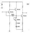
図3は、本発明の好適な一実施の形態によるインダクティブバッファ方式を採用する広帯域増幅器300の概略的な回路図で、広帯域増幅器300は、四つのトランジスタTR301〜TR304、多数個の抵抗、及びインダクタL300を備える。
【0014】
トランジスタTR301は、入力信号を増幅するための第1増幅段として共通エミッタ構造で構成される。第1増幅段TR301が十分な利得を提供することができない場合、他の増幅段、例えば、第2増幅段TR303が更に接続され得る。
【0015】
トランジスタTR302は、第1増幅段TR301と第2増幅段TR303との間に設けられる。この場合、トランジスタTR302は、入力信号をバッファリングするためのバッファ段としての機能を行なう。すなわち、トランジスタTR302は、前段、すなわち、第1増幅段TR301から出力される信号の帯域幅を保持すると共に、該当帯域幅内における利得を増加させる。更に、バッファ段T302は、バッファリングされた信号の一部を、抵抗R301を介して第1増幅段TR301の入力端に戻し、残りのバッファリングされた信号を第2増幅段TR303に転送する。
【0016】
トランジスタTR304は、バッファ段TR302に接続され、このバッファ段TR302をバイアスするためのバイアス段として作用する。バイアス段TR304は、特定の抵抗値を有する抵抗に代えることができる。
多数個の抵抗も、バイアス設計のために用いられており、それぞれの抵抗は特定の抵抗値を有する。
【0017】
一方、インダクタL300は、バイアス段TR304と抵抗R300を介して、バッファ段TR302に接続される。インダクタL300は、インダクティブバッファとして機能を行い、広帯域増幅器300の帯域幅を拡張させる。
【0018】
インダクティブバッファとしての機能を行なうインダクタL300は、広帯域増幅器300の顕著な利得増加及び効果的な帯域幅拡張を提供する。このために、インダクタの最適のインダクタンスは、インダクタのインダクタンスによって変わる利得増加及び帯域幅拡張をシミュレーションすることにより決定される。一方、一般的に、インダクタは半導体チップ上にかなり大きい面積を占め、これにより、インダクタを小さく実現することが好ましい。その故に、利得増加とインダクタの大きさとの間のトレードオフは、インダクタのインダクタンスを決定するとき考慮される必要がある。
【0019】
インダクティブバッファとしての機能を行なうインダクタL300は、半導体チップ上、またはチップの外部のモジュールに接続されているストリップ線路インダクタ上に直接形成され得る。
【0020】
インダクタL300が増幅器300の帯域幅を拡張させる本発明のインダクティブバッファ方式によると、広帯域増幅器300の入力インピーダンスは、周波数が増加するにつれて増加する。インピーダンス増加により、第1増幅段TR301の出力信号が、キルヒホッフの電圧法則によって、他の素子に比較してバッファ段TR302に、より多くの量が印加される。このような現象は、高周波帯域においてより著しくなり、高周波帯域における利得を増加させて帯域幅が拡張できるようにする。
【0021】
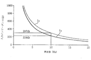
図4は、本発明の好適な実施の形態による広帯域増幅器の上述した特性を示すシミュレーションの結果を示す。
【0022】
図4において、グラフIaは通常の増幅器の入力インピーダンスを示し、グラフIcは図3に示す広帯域増幅器のインピーダンスを示す。x軸は周波数Hzを示し、y軸は入力インピーダンスΩを示す。このシミュレーションで用いられたインダクティブバッファとしての機能を行なうインダクタは、3nHのインダクタンスを有する。
【0023】
シミュレーションの結果からわかるように、10GHzの周波数帯域幅において、本発明の広帯域増幅器300の入力インピーダンスは、通常の増幅器に比べて63Ωだけ増加する。このようなインピーダンス増加は、高周波数帯域における利得を増加させて、上述したように帯域幅を拡張させる。
【0024】
更に、本発明のインダクティブバッファ方式を採用する広帯域増幅器300は利得変化が殆どない。
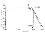
【0025】
図5は、図1に示す従来の広帯域増幅器100及び図3に示す広帯域増幅器300の利得特性グラフを示し、グラフGbは従来の広帯域増幅器100の利得特性グラフ、グラフGcは広帯域増幅器300の利得特性グラフである。x軸は周波数Hzを示し、y軸は伝送インピーダンス利得dBΩを示す。
【0026】
約50dBΩの伝送インピーダンス利得において、従来の広帯域増幅器100は、10.5GHzの帯域幅内で2.1dBΩのオーバーシュートを生成する。しかし、広帯域増幅器300は、同一の10.5GHzの帯域幅内で比較的に均一の利得を表す。すなわち、本発明のインダクティブバッファ方式を採用する広帯域増幅器300は、帯域幅を拡張すると共に、利得変化を殆ど発生しない。
本発明のインダクタL300をバイアス段TR304に提供しさえすれば、従来の技術の増幅器100のインダクタL100の存在はあまり重要ではない。言いかえれば、インダクタL100は、本発明の広帯域増幅器300の動作に実質的に影響を及ぼさず、第1増幅段TR301に実現され得る。
【0027】
さらに、本発明は超高速光通信システムの送受信機のみならず、様々な超高周波回路、すなわち、無線LAN(Local Area Network)、広帯域無線通信網などのような通信サービスに用いられる送受信機の増幅器にも効果的に応用できる。
【0028】
上記において、本発明の好適な実施の形態について説明したが、本発明の請求範囲を逸脱することなく、当業者は種々の改変をなし得るであろう。
【0029】
【発明の効果】
超高周波用素子の開発には多くの時間や費用がかかる。しかし、本発明によれば、急激な利得変化なしに回路の帯域幅を増加することができ、特に、高周波帯域で利得を改善し、ついに帯域幅を増加することができる。
【図面の簡単な説明】
【図1】シャントインダクタ方式を採用する従来の広帯域増幅器の概略的な回路図である。
【図2】通常の増幅器及び図1に示す従来の広帯域増幅器の利得特性グラフである。
【図3】本発明の好適な実施の形態による広帯域増幅器の概略的な回路図である。
【図4】通常の増幅器及び図3に示す本発明の広帯域増幅器の入力インピーダンスを示す。
【図5】図1に示す従来の広帯域増幅器及び図3に示す本発明の広帯域増幅器の伝送インピーダンスを示す特性グラフを示す。
【符号の説明】
TR101、TR103、TR301、TR303…増幅用トランジスタ、TR102、TR302、TR304…バッファ用トランジスタ、TR104…バイアス用トランジスタ、L100…インダクタ、L300…インダクティブバッファ。[0001]
TECHNICAL FIELD OF THE INVENTION
The present invention relates to a broadband amplifying device, and more particularly, to a wideband amplifying device for extending a bandwidth using an inductive buffer.
[0002]
[Prior art]
Recently, ultra-high-speed data communication technology, for example, optical communication technology using an optical fiber has been rapidly growing, and accordingly, a demand for a data transmission amount has been increased. In order to transfer large amounts of data, it is essential to implement a broadband amplifier that operates with a wider bandwidth. For this reason, it is necessary to develop an active element that can operate stably in an ultra-high frequency band. However, it takes a long time and high cost to develop such a new active element, so how to provide a newly developed element and others in a broadband amplifier circuit, that is, a newly developed element It is also important to improve the way that wideband amplifier circuits are designed to operate efficiently.
[0003]
Typically, a shunt inductor scheme is used to design a broadband amplifier circuit.
[0004]
FIG. 1 is a schematic circuit diagram of a
[0005]
According to the shunt inductor method described above, a resonance phenomenon occurs between the inductor L100 and a parasitic capacitor on a pad (not shown). The resonance phenomenon increases the impedance at the load end of the
[0006]
However, the shunt inductor scheme, along with gain gain and bandwidth extension, involves significant gain peaking that can degrade the performance of the amplifier. Such a gain characteristic is shown in FIG.
[0007]
FIG. 2 shows a gain characteristic graph of the conventional amplifier and the
[0008]
At a transmission impedance of about 50 dBΩ, a conventional broadband amplifier has a larger effective bandwidth of 10.5 GHz compared to a normal amplifier having a bandwidth of 8.4 GHz. However, as can be seen from the graph, this has significant gain peaking of 2 dBΩ or more. Such significant gain changes in the effective bandwidth over which the data is processed may exceed the maximum allowable input voltage of the subsequently connected limiting amplifier and cause operational errors.
[0009]
Therefore, there is a need for a bandwidth extension method for obtaining sufficient bandwidth extension with little gain change.
[0010]
[Problems to be solved by the invention]
The present invention has been made in view of the above circumstances, and an object of the present invention is to provide an amplifying device that has almost no gain change and can extend the bandwidth.
[0011]
[Means for Solving the Problems]
In order to achieve the above object, an embodiment of the present invention is a broadband amplifying device for extending a bandwidth, comprising a first and a second amplifying element for amplifying an input signal; The first amplifier element is provided between the first amplifier element and the second amplifier element to maintain a bandwidth of an output signal, increase a gain, and return a part of the buffered signal to the first amplifier element. A buffering element for buffering the output signal of the amplifying element and the buffering element are connected to each other, so as to extend the bandwidth and show almost no gain change, as the frequency increases within a predetermined range so as to show almost no gain change. Provided is a wideband amplifier including a first inductive buffer for increasing input impedance.
[0012]
BEST MODE FOR CARRYING OUT THE INVENTION
Hereinafter, preferred embodiments of the present invention will be described in detail with reference to the drawings.
[0013]
FIG. 3 is a schematic circuit diagram of a
[0014]
The transistor TR301 has a common emitter structure as a first amplification stage for amplifying an input signal. If the first amplification stage TR301 cannot provide sufficient gain, another amplification stage, for example, the second amplification stage TR303 can be further connected.
[0015]
The transistor TR302 is provided between the first amplification stage TR301 and the second amplification stage TR303. In this case, transistor TR302 functions as a buffer stage for buffering an input signal. That is, the transistor TR302 holds the bandwidth of the signal output from the previous stage, that is, the first amplification stage TR301, and increases the gain within the bandwidth. Further, the buffer stage T302 returns a part of the buffered signal to the input terminal of the first amplification stage TR301 via the resistor R301, and transfers the remaining buffered signal to the second amplification stage TR303.
[0016]
Transistor TR304 is connected to buffer stage TR302 and acts as a bias stage for biasing buffer stage TR302. The bias stage TR304 can be replaced with a resistor having a specific resistance value.
A number of resistors are also used for the bias design, each having a specific resistance value.
[0017]
On the other hand, the inductor L300 is connected to the buffer stage TR302 via the bias stage TR304 and the resistor R300. Inductor L300 functions as an inductive buffer to extend the bandwidth of
[0018]
Inductor L300, acting as an inductive buffer, provides a significant gain increase and effective bandwidth extension of
[0019]
Inductor L300, which acts as an inductive buffer, can be formed directly on a semiconductor chip, or on a stripline inductor connected to a module external to the chip.
[0020]
According to the inductive buffer scheme of the present invention in which the inductor L300 extends the bandwidth of the
[0021]
FIG. 4 shows the results of a simulation showing the above characteristics of a broadband amplifier according to a preferred embodiment of the present invention.
[0022]
In FIG. 4, a graph Ia shows the input impedance of a normal amplifier, and a graph Ic shows the impedance of the broadband amplifier shown in FIG. The x-axis indicates frequency Hz, and the y-axis indicates input impedance Ω. The inductor used as an inductive buffer used in this simulation has an inductance of 3 nH.
[0023]
As can be seen from the simulation results, in the frequency bandwidth of 10 GHz, the input impedance of the
[0024]
Further, the
[0025]
FIG. 5 is a graph showing gain characteristics of the conventional
[0026]
At a transmission impedance gain of about 50 dBΩ, the
As long as the inductor L300 of the present invention is provided to the bias stage TR304, the presence of the inductor L100 of the
[0027]
Furthermore, the present invention is applicable not only to a transceiver for an ultra-high-speed optical communication system, but also to an amplifier for a transceiver used for various ultra-high frequency circuits, that is, for a communication service such as a wireless LAN (Local Area Network), a broadband wireless communication network, or the like. Can also be applied effectively.
[0028]
Although the preferred embodiments of the present invention have been described above, those skilled in the art will be able to make various modifications without departing from the scope of the present invention.
[0029]
【The invention's effect】
It takes a lot of time and money to develop an ultra-high frequency device. However, according to the present invention, the bandwidth of the circuit can be increased without a sudden change in gain, and in particular, the gain can be improved in a high frequency band, and finally the bandwidth can be increased.
[Brief description of the drawings]
FIG. 1 is a schematic circuit diagram of a conventional wideband amplifier employing a shunt inductor system.
FIG. 2 is a graph illustrating gain characteristics of a normal amplifier and the conventional wideband amplifier illustrated in FIG. 1;
FIG. 3 is a schematic circuit diagram of a broadband amplifier according to a preferred embodiment of the present invention;
FIG. 4 shows the input impedance of a conventional amplifier and the broadband amplifier of the present invention shown in FIG.
5 is a characteristic graph showing the transmission impedance of the conventional wide-band amplifier shown in FIG. 1 and the wide-band amplifier of the present invention shown in FIG. 3;
[Explanation of symbols]
TR101, TR103, TR301, TR303: amplifying transistor, TR102, TR302, TR304: buffer transistor, TR104: bias transistor, L100: inductor, L300: inductive buffer.
Claims (8)
入力信号を増幅するための第1及び第2増幅素子と、
前記第1増幅素子と前記第2増幅素子との間に設けられ、出力信号の帯域幅を保持し、利得を増加し、バッファリングされた信号の一部を前記第1増幅素子に戻すことにより、前記第1増幅素子の出力信号をバッファリングするためのバッファリング素子と、
前記バッファリング素子に接続されており、帯域幅を拡張すると共に、利得変化を殆ど示さないように、周波数が所定範囲内で増加するにつれて、入力インピーダンスを増加させるための第1インダクティブバッファとを具備する広帯域増幅装置。A broadband amplifier for extending the bandwidth,
First and second amplifying elements for amplifying an input signal;
Provided between the first amplifying element and the second amplifying element, maintaining the bandwidth of the output signal, increasing the gain, and returning a part of the buffered signal to the first amplifying element. A buffering element for buffering an output signal of the first amplifying element;
A first inductive buffer connected to the buffering element for increasing the input impedance as the frequency increases within a predetermined range so as to extend the bandwidth and show little gain change. Broadband amplifier.
Applications Claiming Priority (1)
| Application Number | Priority Date | Filing Date | Title |
|---|---|---|---|
| KR10-2002-0038866A KR100459064B1 (en) | 2002-07-05 | 2002-07-05 | Bandwidth expansion circuit of broadband amplifier |
Publications (1)
| Publication Number | Publication Date |
|---|---|
| JP2004040799A true JP2004040799A (en) | 2004-02-05 |
Family
ID=27727176
Family Applications (1)
| Application Number | Title | Priority Date | Filing Date |
|---|---|---|---|
| JP2003191732A Pending JP2004040799A (en) | 2002-07-05 | 2003-07-04 | Wideband amplifier for bandwidth expansion |
Country Status (3)
| Country | Link |
|---|---|
| US (1) | US6914488B2 (en) |
| JP (1) | JP2004040799A (en) |
| KR (1) | KR100459064B1 (en) |
Cited By (1)
| Publication number | Priority date | Publication date | Assignee | Title |
|---|---|---|---|---|
| WO2013011685A1 (en) * | 2011-07-19 | 2013-01-24 | パナソニック株式会社 | High-frequency power amplifier |
Families Citing this family (3)
| Publication number | Priority date | Publication date | Assignee | Title |
|---|---|---|---|---|
| US7411454B1 (en) * | 2007-01-19 | 2008-08-12 | Chattin Daniel A | Electron turbulence damping circuit for a complimentary-symmetry amplification unit |
| KR100906244B1 (en) * | 2007-08-28 | 2009-07-07 | 전자부품연구원 | Rf amplifier and method amplifing using thereof |
| KR200452004Y1 (en) * | 2008-07-02 | 2011-01-25 | 부인산업(주) | Paper bag with cover |
Family Cites Families (9)
| Publication number | Priority date | Publication date | Assignee | Title |
|---|---|---|---|---|
| FR2560468A1 (en) * | 1984-02-28 | 1985-08-30 | Lgt Lab Gen Telecomm | TRANSISTOR AMPLIFIER STAGE POLARIZATION DEVICE AND ITS USE IN SUCH A FLOOR |
| JPH03217108A (en) * | 1990-01-23 | 1991-09-24 | Toshiba Corp | Peaking circuit |
| JPH05315865A (en) * | 1992-05-13 | 1993-11-26 | Hitachi Ltd | Broadband amplifier |
| US5406226A (en) * | 1993-07-07 | 1995-04-11 | Wireless Access, Inc. | Stable, narrow bandwidth, high frequency amplifier with low power consumption |
| EP1014565B1 (en) * | 1998-12-22 | 2006-05-10 | STMicroelectronics S.r.l. | Low-noise amplifier stage with matching network |
| US6204728B1 (en) * | 1999-01-28 | 2001-03-20 | Maxim Integrated Products, Inc. | Radio frequency amplifier with reduced intermodulation distortion |
| KR100329213B1 (en) * | 1999-07-20 | 2002-03-22 | 전종한 | Composition for Preparing Conductive Polyurethanes |
| US6265944B1 (en) * | 1999-09-27 | 2001-07-24 | Conexant Systems, Inc. | Fully integrated broadband RF voltage amplifier with enhanced voltage gain and method |
| JP2001326544A (en) * | 2000-05-16 | 2001-11-22 | Shinya Kojima | Broadband optical receiver |
-
2002
- 2002-07-05 KR KR10-2002-0038866A patent/KR100459064B1/en not_active Expired - Fee Related
-
2003
- 2003-07-03 US US10/613,362 patent/US6914488B2/en not_active Expired - Fee Related
- 2003-07-04 JP JP2003191732A patent/JP2004040799A/en active Pending
Cited By (1)
| Publication number | Priority date | Publication date | Assignee | Title |
|---|---|---|---|---|
| WO2013011685A1 (en) * | 2011-07-19 | 2013-01-24 | パナソニック株式会社 | High-frequency power amplifier |
Also Published As
| Publication number | Publication date |
|---|---|
| KR20020064721A (en) | 2002-08-09 |
| KR100459064B1 (en) | 2004-12-03 |
| US20040004519A1 (en) | 2004-01-08 |
| US6914488B2 (en) | 2005-07-05 |
Similar Documents
| Publication | Publication Date | Title |
|---|---|---|
| US6472941B2 (en) | Distributed amplifier with terminating circuit capable of improving gain flatness at low frequencies | |
| JP3663397B2 (en) | High frequency power amplifier | |
| JP4751002B2 (en) | Cascode type distributed amplifier | |
| CN110311632B (en) | Self-adaptive bias circuit with high-temperature drift inhibition capability | |
| JP4377652B2 (en) | Driver circuit | |
| JP2015122628A (en) | Switching circuit and semiconductor module | |
| JP4570339B2 (en) | Ultra-wideband distributed amplifier with active loading device for bias application | |
| US9735989B1 (en) | Continuous time linear equalizer that uses cross-coupled cascodes and inductive peaking | |
| Bierbuesse et al. | 60 GHz variable gain & linearity enhancement LNA in 65 nm CMOS | |
| US7119617B2 (en) | Differential amplifier | |
| KR100830812B1 (en) | High frequency amplifier circuit | |
| US6456163B1 (en) | High-frequency amplifier circuit having a directly-connected bias circuit | |
| US6664853B1 (en) | Wide-bandwidth differential signal amplifier | |
| EP1421679A2 (en) | High frequency power amplifier circuit | |
| JP2004040799A (en) | Wideband amplifier for bandwidth expansion | |
| US6930557B2 (en) | Multi-stage amplifier | |
| US7956692B2 (en) | Wide-band amplifier circuit with improved gain flatness | |
| JP2004201313A (en) | Transmission impedance amplifying device of source follower structure | |
| KR100375520B1 (en) | Linearizer | |
| CN101527542A (en) | Multi-stage amplifier circuit, method and integrated circuit for minimizing common mode oscillation | |
| JP2004159195A (en) | Amplifier circuit | |
| US6593811B2 (en) | Nonlinear feedback linearizer | |
| JPH08265065A (en) | Amplifier circuit | |
| JP2015154483A (en) | Receiver circuit, optical receiver, and return-loss reduction method | |
| JPH11274870A (en) | High frequency circuit device |
Legal Events
| Date | Code | Title | Description |
|---|---|---|---|
| A521 | Written amendment |
Free format text: JAPANESE INTERMEDIATE CODE: A523 Effective date: 20040310 |
|
| A977 | Report on retrieval |
Free format text: JAPANESE INTERMEDIATE CODE: A971007 Effective date: 20060627 |
|
| A131 | Notification of reasons for refusal |
Free format text: JAPANESE INTERMEDIATE CODE: A131 Effective date: 20060801 |
|
| A521 | Written amendment |
Free format text: JAPANESE INTERMEDIATE CODE: A523 Effective date: 20061101 |
|
| A131 | Notification of reasons for refusal |
Free format text: JAPANESE INTERMEDIATE CODE: A131 Effective date: 20070220 |
|
| A02 | Decision of refusal |
Free format text: JAPANESE INTERMEDIATE CODE: A02 Effective date: 20070710 |