JP2004031663A - Wiring structure of jumper wire - Google Patents
Wiring structure of jumper wire Download PDFInfo
- Publication number
- JP2004031663A JP2004031663A JP2002186203A JP2002186203A JP2004031663A JP 2004031663 A JP2004031663 A JP 2004031663A JP 2002186203 A JP2002186203 A JP 2002186203A JP 2002186203 A JP2002186203 A JP 2002186203A JP 2004031663 A JP2004031663 A JP 2004031663A
- Authority
- JP
- Japan
- Prior art keywords
- jumper
- circuit board
- printed circuit
- jumper wire
- fitted
- Prior art date
- Legal status (The legal status is an assumption and is not a legal conclusion. Google has not performed a legal analysis and makes no representation as to the accuracy of the status listed.)
- Granted
Links
- 239000004020 conductor Substances 0.000 claims abstract description 11
- 230000000149 penetrating effect Effects 0.000 abstract description 2
- 238000005452 bending Methods 0.000 abstract 1
- 230000000694 effects Effects 0.000 description 2
- 230000005855 radiation Effects 0.000 description 2
- 239000003990 capacitor Substances 0.000 description 1
- 238000003672 processing method Methods 0.000 description 1
Images
Classifications
-
- H—ELECTRICITY
- H05—ELECTRIC TECHNIQUES NOT OTHERWISE PROVIDED FOR
- H05K—PRINTED CIRCUITS; CASINGS OR CONSTRUCTIONAL DETAILS OF ELECTRIC APPARATUS; MANUFACTURE OF ASSEMBLAGES OF ELECTRICAL COMPONENTS
- H05K3/00—Apparatus or processes for manufacturing printed circuits
- H05K3/22—Secondary treatment of printed circuits
- H05K3/222—Completing of printed circuits by adding non-printed jumper connections
-
- H—ELECTRICITY
- H01—ELECTRIC ELEMENTS
- H01R—ELECTRICALLY-CONDUCTIVE CONNECTIONS; STRUCTURAL ASSOCIATIONS OF A PLURALITY OF MUTUALLY-INSULATED ELECTRICAL CONNECTING ELEMENTS; COUPLING DEVICES; CURRENT COLLECTORS
- H01R31/00—Coupling parts supported only by co-operation with counterpart
- H01R31/08—Short-circuiting members for bridging contacts in a counterpart
Landscapes
- Engineering & Computer Science (AREA)
- Manufacturing & Machinery (AREA)
- Microelectronics & Electronic Packaging (AREA)
- Structure Of Printed Boards (AREA)
- Multi-Conductor Connections (AREA)
- Coupling Device And Connection With Printed Circuit (AREA)
- Printing Elements For Providing Electric Connections Between Printed Circuits (AREA)
Abstract
Description
【0001】
【発明の属する技術分野】
本発明はジャンパ線をプリント基板に効率良く配線する構造に関するものである。
【0002】
【従来の技術】
一般には、プリント基板の裏面には所定の導体パターンが設けられ、導体パターンを有していない表側にはCPU、ROM等のIC、又コンデンサー、抵抗、ダイオード、トランジスター等の各種電子部品が取付けられている。そしてこれら各電子部品を接続するジャンパ線が配線されて裏面の導体パターンに接続している。
【0003】
上記各電子部品を導体パターンに接続するにはプリント基板の上に配置し、接続端子を端子穴から下面側へ突出して導体パターンにハンダ付けしている。又、プリント基板を貫通する穴を設け、ジャンパ線の両端部を該穴に挿通して先端を導体パターンにハンダ付けしている。このように、プリント基板上には各電子部品及びジャンパ線が配置されて煩雑化し、部品の配置が制限されると共に一方ではプリント基板の配置面積が大きくなってしまう。
【0004】
そこで、プリント基板上の電子部品及びジャンパ線、これらと交差する方向に配置した飛びジャンパ線とを設けて、これらのジャンパ線を立体配置することにより、高密度実装が出来る為にプリント基板サイズ及び配置面積を小さくし、配線が最短距離で出来る為に電波の輻射及びノイズを低減することが出来るようにしたジャンパ線の立体配置構造が知られている(特開平6−334290号)。
【0005】
すなわち、上記「ジャンパ線の立体配置構造」は「裏面にプリント配線をしたプリント配線基板と、該プリント配線基板の表面上の第1区画から離れた第2区画に配置され電気的に接続する少なくとも1つのジャンパ線と、該ジャンパ線と交差する方向にある第3区画及び第4区画の間を連結し前記ジャンパ線から隔離して立体配置した少なくとも1つの飛びジャンパ線とを備えている。」
【0006】
しかし、上記特開平6−334290号に係る「ジャンパ線の立体配置構造」は、図5(a)に示しているように複数のジャンパ線が平行に並んで配置される場合、ジャンパ線に外力が作用するならば、ジャンパ線同士が互いに接触して電気回路が短絡する虞がある。又図5(b)に示しているように複数の飛びジャンパ線が平行に並んで配置された場合、飛びジャンパ線に外力が作用するならば、飛びジャンパ線同士が接触して電気回路が短絡する虞がある。
【0007】
【発明が解決しようとする課題】
このように、従来のジャンパ線の配線構造には上記のごとき問題がある。本発明が解決しようとする課題はこれら問題点であり、平行に配線された複数のジャンパ線が互いに接触して短絡することがないように、又クロスして配線されたジャンパ線が互いに接触して短絡しないように構成したジャンパ線の配線構造を提供する。
【0008】
【課題を解決する為の手段】
本発明のジャンパ線配線構造は、プリント基板の上面にジャンパ線を配線するのではなく、プリント基板の上面にスリット溝を形成し、このスリット溝にジャンパ線を嵌入して配線する。そこで、複数本のジャンパ線を平行に配線する場合、全てのジャンパ線が嵌るスリット溝を形成する場合、又は交互にスリット溝を形成して嵌入する場合の何れでもよい。
【0009】
そして、交差してジャンパ線を配線する場合には、下側に位置する1本ないし複数本のジャンパ線はスリット溝に嵌入し、上側のジャンパ線はプリント基板の上面に配線する。ここで、上側のプリント基板上面に配線するジャンパ線はシールする場合もある。一方、スリット溝に嵌ったジャンパ線の上側には他の電子部品を取付けることも出来る。以下、本発明に係る実施例を図面に基づいて詳細に説明する。
【0010】
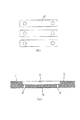
【実施例】
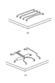
図1は本発明に係るジャンパ線の配線構造を構成する為のプリント基板1を示している実施例であり、(a)は平面図、(b)は断面図である。プリント基板1の下面4には導体パターンが形成され、上面5の所定の位置にはスリット溝2,2…が設けられている。そして該スリット溝2,2…の両端には端子穴3,3…が下面4ヘ貫通している。ここで、スリット溝2,2…の加工方法は限定しないことにするが、一般的にはスリット溝幅のエンドミルを使用して切削加工される。
【0011】
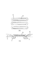
図2は上記スリット溝2,2…にジャンパ線6,6…を嵌めて配線した場合であり、本発明の具体例を示している。ジャンパ線6はその両端部7,7を屈曲してプリント基板1の端子穴3,3に嵌め、先端を夫々内側へ折り曲げて導体パターンにハンダ付けしている。このように各ジャンパ線6,6…がスリット溝2,2…に嵌ることで、外力が作用しても変形することはなく、勿論、隣のジャンパ線6に接して短絡することもあり得ない。
【0012】
同図(b)に示すように、ジャンパ線6,6…はスリット溝2,2…に完全に嵌って配線されているが、上面5側へ一部突出する場合もある。しかし、ジャンパ線6の大部分がスリット溝2に嵌っていれば、変形して隣のジャンパ線6に接触することはない。
【0013】
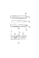
図3は本発明に係る他の実施例であり、平行に配線されている3本のジャンパ線6a,6b,6cの内、両側の2本のジャンパ線6a,6cはスリット溝2a,2cに嵌っている。しかし中央に位置するジャンパ線6bはプリント基板上面5に直接配線されている。これらジャンパ線6a,6b,6cの間隔がある程度隔たっていると共に、両側のジャンパ線6a,6cがスリット溝2a,2cに完全に嵌っている場合であるならば、中央のジャンパ線6bがスリット溝2に嵌めなくても互いに接触する危険性は少ない。
【0014】
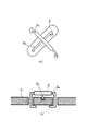
図4は本発明に係るさらに別の実施例を示している。このジャンパ線6a,6bは互いにクロスして配線されている。そして両ジャンパ線6a,6bが接触して短絡しないように、一方のジャンパ線6aはスリット溝2に嵌って配線され、他方のジャンパ線6bはプリント基板1の上面5に載って配線されている。スリット溝2に嵌っているジャンパ線6aは上面5から突出しないようにしているが、上側に配線されるジャンパ線6bが上方から押されてスリット溝2内のジャンパ線6aに接しないように、該ジャンパ線6bの周りにはシール8が設けられている。
【0015】
上記図4に示す実施例では、スリット溝2に嵌っているジャンパ線6aとプリント基板1の上面5に配置されるジャンパ線6bが互いにクロスしている場合であるが、ジャンパ線6bの代わりに他の電子部品をクロスして取付けることも出来る。
【0016】
以上述べたように、本発明に係るジャンパ線の配線構造は、プリント基板の上面に形成したスリット溝にジャンパ線を嵌めたものであり、次のような効果を得ることが出来る。
【0017】
【発明の効果】
プリント基板に複数本のジャンパ線を配線する場合、ジャンパ線はスリット溝に嵌って隣り合うジャンパ線に接触して短絡することはない為に、小さなプリント基板に高密度で配線することが出来る。従って、プリント基板での配線面積を小さくし、プリント基板の縮小を図ることが出来る。その結果、ジャンパ線を最短距離で配線出来る為に、電磁波の輻射を小さくし、ノイズの低減を図ることが可能である。
【0018】
そして、ジャンパ線はスリット溝に嵌ることで、クロスしてジャンパ線を配線する場合に形状の異なる飛びジャンパ線を使う必要がなく、部品の使い分けは必要ない。従って、ジャンパ線の配線作業は簡単となって、作業性は向上する。又、スリット溝に嵌ったジャンパ線の上側には他の電子部品をクロスして取付けることも出来る。
【図面の簡単な説明】
【図1】上面にスリット溝を形成したプリント基板。
【図2】スリット溝にジャンパ線を嵌めて取付けた配線構造。
【図3】スリット溝にジャンパ線を嵌めて取付けた配線構造。
【図4】スリット溝にジャンパ線を嵌めて取付けたクロス配線構造。
【図5】従来のジャンパ線の配線構造。
【符号の説明】
1 プリント基板
2 スリット溝
3 端子穴
4 下面
5 上面
6 ジャンパ線
7 端部
8 シール[0001]
TECHNICAL FIELD OF THE INVENTION
The present invention relates to a structure for efficiently wiring jumper wires to a printed circuit board.
[0002]
[Prior art]
In general, a predetermined conductor pattern is provided on the back surface of a printed circuit board, and ICs such as a CPU and a ROM, and various electronic components such as capacitors, resistors, diodes, and transistors are mounted on the front side having no conductor pattern. ing. A jumper wire connecting these electronic components is wired and connected to the conductor pattern on the back surface.
[0003]
In order to connect the electronic components to the conductor pattern, the electronic components are arranged on a printed circuit board, and connection terminals are soldered to the conductor pattern by protruding from the terminal holes to the lower surface side. Further, a hole penetrating the printed circuit board is provided, and both ends of the jumper wire are inserted into the hole, and the end is soldered to the conductor pattern. As described above, the electronic components and the jumper wires are arranged on the printed circuit board to complicate the arrangement, and the arrangement of the components is restricted, and at the same time, the arrangement area of the printed circuit board is increased.
[0004]
Therefore, electronic components and jumper wires on the printed circuit board, jump jumper wires arranged in a direction intersecting these are provided, and these jumper wires are three-dimensionally arranged. There is known a three-dimensional arrangement structure of jumper wires in which the arrangement area is reduced and the wiring can be formed at the shortest distance, so that radiation and noise of radio waves can be reduced (Japanese Patent Laid-Open No. 6-334290).
[0005]
That is, the “three-dimensional arrangement structure of jumper lines” is defined as “at least a printed wiring board having printed wiring on the back surface, and a second wiring section disposed on the front surface of the printed wiring board and separated from the first wiring section and electrically connected thereto. It has one jumper line and at least one jumper line which connects the third section and the fourth section in a direction intersecting the jumper line and is three-dimensionally arranged so as to be separated from the jumper line. "
[0006]
However, the "three-dimensional configuration of jumper wires" disclosed in Japanese Patent Application Laid-Open No. 6-334290 does not apply an external force to the jumper wires when a plurality of jumper wires are arranged in parallel as shown in FIG. If there is a possibility that the jumper wires will come into contact with each other, the electric circuit may be short-circuited. When a plurality of jumper jumpers are arranged in parallel as shown in FIG. 5B, if an external force acts on the jumper jumpers, the jumper jumpers will come into contact with each other to short-circuit the electric circuit. There is a risk of doing so.
[0007]
[Problems to be solved by the invention]
As described above, the conventional jumper wiring structure has the above-described problem. The problems to be solved by the present invention are these problems, so that a plurality of jumper wires wired in parallel do not touch each other and short-circuit, and jumper wires wired crosswise contact each other. Provided is a wiring structure of a jumper wire configured so as not to short-circuit.
[0008]
[Means for solving the problem]
In the jumper line wiring structure of the present invention, a slit groove is formed on the upper surface of the printed circuit board instead of wiring the jumper line on the upper surface of the printed circuit board, and the jumper line is inserted into the slit groove and wired. Therefore, either a case in which a plurality of jumper lines are wired in parallel, a case in which slit grooves in which all jumper lines are fitted, or a case in which slit grooves are formed alternately and fitted therein may be used.
[0009]
When the jumper wires are crossed, one or more lower jumper wires are fitted into the slit grooves, and the upper jumper wire is wired on the upper surface of the printed circuit board. Here, a jumper line wired on the upper surface of the upper printed circuit board may be sealed. On the other hand, other electronic components can be mounted above the jumper wire fitted in the slit groove. Hereinafter, embodiments according to the present invention will be described in detail with reference to the drawings.
[0010]
【Example】
FIG. 1 is an embodiment showing a printed circuit board 1 for forming a wiring structure of jumper wires according to the present invention, wherein FIG. 1 (a) is a plan view and FIG. 1 (b) is a sectional view. A conductive pattern is formed on the
[0011]
FIG. 2 shows a case in which
[0012]
As shown in FIG. 1B, the
[0013]
FIG. 3 shows another embodiment according to the present invention. Of the three
[0014]
FIG. 4 shows still another embodiment according to the present invention. The jumper lines 6a and 6b are wired crossing each other. One jumper wire 6a is fitted in the
[0015]
In the embodiment shown in FIG. 4, the jumper wire 6a fitted in the
[0016]
As described above, the jumper wire wiring structure according to the present invention has the jumper wires fitted in the slit grooves formed on the upper surface of the printed circuit board, and can provide the following effects.
[0017]
【The invention's effect】
When a plurality of jumper lines are wired on a printed circuit board, the jumper lines are fitted into the slit grooves and do not contact adjacent jumper lines to short-circuit, so that high-density wiring can be performed on a small printed circuit board. Therefore, the wiring area on the printed board can be reduced, and the printed board can be reduced in size. As a result, since the jumper wire can be wired in the shortest distance, it is possible to reduce the radiation of the electromagnetic wave and reduce the noise.
[0018]
The jumper wires are fitted in the slit grooves, so that when jumper wires are crossed and wired, it is not necessary to use jump jumper wires having different shapes, and it is not necessary to use different components. Therefore, the wiring work of the jumper wire is simplified, and the workability is improved. Further, another electronic component can be mounted crosswise on the upper side of the jumper wire fitted in the slit groove.
[Brief description of the drawings]
FIG. 1 is a printed circuit board having a slit groove formed on an upper surface.
FIG. 2 is a wiring structure in which a jumper wire is fitted into a slit groove and attached.
FIG. 3 shows a wiring structure in which a jumper wire is fitted into a slit groove and attached.
FIG. 4 is a cross wiring structure in which a jumper wire is fitted in a slit groove and attached.
FIG. 5 shows a conventional wiring structure of a jumper line.
[Explanation of symbols]
DESCRIPTION OF SYMBOLS 1 Printed
Claims (4)
Priority Applications (2)
| Application Number | Priority Date | Filing Date | Title |
|---|---|---|---|
| JP2002186203A JP3610493B2 (en) | 2002-06-26 | 2002-06-26 | Jumper wiring structure |
| US10/452,584 US6899560B2 (en) | 2002-06-26 | 2003-06-03 | Jump wire structure |
Applications Claiming Priority (1)
| Application Number | Priority Date | Filing Date | Title |
|---|---|---|---|
| JP2002186203A JP3610493B2 (en) | 2002-06-26 | 2002-06-26 | Jumper wiring structure |
Publications (2)
| Publication Number | Publication Date |
|---|---|
| JP2004031663A true JP2004031663A (en) | 2004-01-29 |
| JP3610493B2 JP3610493B2 (en) | 2005-01-12 |
Family
ID=29774132
Family Applications (1)
| Application Number | Title | Priority Date | Filing Date |
|---|---|---|---|
| JP2002186203A Expired - Fee Related JP3610493B2 (en) | 2002-06-26 | 2002-06-26 | Jumper wiring structure |
Country Status (2)
| Country | Link |
|---|---|
| US (1) | US6899560B2 (en) |
| JP (1) | JP3610493B2 (en) |
Families Citing this family (3)
| Publication number | Priority date | Publication date | Assignee | Title |
|---|---|---|---|---|
| US8087953B2 (en) * | 2008-04-01 | 2012-01-03 | Sony Corporation | Surface mount device jumper and surface mount device jumper assembly |
| US9907908B2 (en) | 2011-03-08 | 2018-03-06 | Baxter International Inc. | Non-invasive radio frequency medical fluid level and volume detection system and method |
| CN103338584A (en) * | 2013-06-20 | 2013-10-02 | 张家港市华为电子有限公司 | Crossover line component for PCB |
Family Cites Families (7)
| Publication number | Priority date | Publication date | Assignee | Title |
|---|---|---|---|---|
| US2389255A (en) * | 1941-10-22 | 1945-11-20 | Gen Cable Corp | Connector |
| US4335272A (en) * | 1980-07-28 | 1982-06-15 | Zenith Radio Corporation | Breakaway circuit board with flexible coupling |
| US4859807A (en) * | 1985-07-19 | 1989-08-22 | Kollmorgen Technologies Corporation | Wire scribed circuit boards and method of manufacture |
| JPH05218607A (en) * | 1992-01-31 | 1993-08-27 | Sony Corp | Printed-circuit board |
| JPH06334290A (en) | 1993-05-20 | 1994-12-02 | Funai Electric Co Ltd | Multilevel intersection structure of jumper wire |
| US5446961A (en) * | 1993-10-15 | 1995-09-05 | International Business Machines Corporation | Method for repairing semiconductor substrates |
| US5357051A (en) * | 1994-01-31 | 1994-10-18 | Hwang Richard H | Printed circuit board for reducing radio frequency interferences |
-
2002
- 2002-06-26 JP JP2002186203A patent/JP3610493B2/en not_active Expired - Fee Related
-
2003
- 2003-06-03 US US10/452,584 patent/US6899560B2/en not_active Expired - Fee Related
Also Published As
| Publication number | Publication date |
|---|---|
| US6899560B2 (en) | 2005-05-31 |
| JP3610493B2 (en) | 2005-01-12 |
| US20040002257A1 (en) | 2004-01-01 |
Similar Documents
| Publication | Publication Date | Title |
|---|---|---|
| KR20020050713A (en) | Flat flexible circuit interconnections | |
| JP7175632B2 (en) | Shunt Resistor and Shunt Resistor Mounting Structure | |
| TWM593101U (en) | Circuit device | |
| JP2004031663A (en) | Wiring structure of jumper wire | |
| EP0737025A4 (en) | PRINTED CIRCUIT BOARD | |
| CN106471870A (en) | Circuit structure | |
| JP2000269667A (en) | Electrical connection box | |
| JP2017139394A (en) | Electric connection structure and method for electronic circuit board and fpc | |
| JP2005033882A (en) | Circuit structure of electric connection box | |
| JPH06164091A (en) | Circuit board | |
| JPH05102621A (en) | Conductive pattern | |
| EP1647051B1 (en) | Semiconductor power module with strip conductors which are detached from a substrate as external connections | |
| KR200188982Y1 (en) | Circuit board | |
| JP3137912B2 (en) | Printed circuit structure | |
| JP2008166471A (en) | Substrate for wiring | |
| JP2002118333A (en) | Noise-proof circuit and its manufacturing method | |
| JP2007194240A (en) | Printed circuit boards and electronic devices | |
| TWI559628B (en) | Electrical connector of the circuit board | |
| KR100818464B1 (en) | Smd type array jumper | |
| KR200230496Y1 (en) | Circuit board | |
| JP2002050839A (en) | Electronic apparatus | |
| JP2005136182A (en) | Flexible wiring board | |
| JP2007116039A (en) | Circuit board | |
| JPH114052A (en) | Printed wiring board | |
| JPH06232522A (en) | Printed wiring board |
Legal Events
| Date | Code | Title | Description |
|---|---|---|---|
| A621 | Written request for application examination |
Free format text: JAPANESE INTERMEDIATE CODE: A621 Effective date: 20040205 |
|
| A131 | Notification of reasons for refusal |
Free format text: JAPANESE INTERMEDIATE CODE: A131 Effective date: 20040608 |
|
| A521 | Request for written amendment filed |
Free format text: JAPANESE INTERMEDIATE CODE: A523 Effective date: 20040806 |
|
| TRDD | Decision of grant or rejection written | ||
| A01 | Written decision to grant a patent or to grant a registration (utility model) |
Free format text: JAPANESE INTERMEDIATE CODE: A01 Effective date: 20040921 |
|
| A61 | First payment of annual fees (during grant procedure) |
Free format text: JAPANESE INTERMEDIATE CODE: A61 Effective date: 20041006 |
|
| R150 | Certificate of patent or registration of utility model |
Free format text: JAPANESE INTERMEDIATE CODE: R150 |
|
| LAPS | Cancellation because of no payment of annual fees |