JP2004005965A - Magnetic memory device of small area - Google Patents
Magnetic memory device of small area Download PDFInfo
- Publication number
- JP2004005965A JP2004005965A JP2003131176A JP2003131176A JP2004005965A JP 2004005965 A JP2004005965 A JP 2004005965A JP 2003131176 A JP2003131176 A JP 2003131176A JP 2003131176 A JP2003131176 A JP 2003131176A JP 2004005965 A JP2004005965 A JP 2004005965A
- Authority
- JP
- Japan
- Prior art keywords
- write
- conductor
- memory device
- magnetic
- memory cell
- Prior art date
- Legal status (The legal status is an assumption and is not a legal conclusion. Google has not performed a legal analysis and makes no representation as to the accuracy of the status listed.)
- Pending
Links
Images


Classifications
-
- G—PHYSICS
- G11—INFORMATION STORAGE
- G11C—STATIC STORES
- G11C11/00—Digital stores characterised by the use of particular electric or magnetic storage elements; Storage elements therefor
- G11C11/02—Digital stores characterised by the use of particular electric or magnetic storage elements; Storage elements therefor using magnetic elements
- G11C11/16—Digital stores characterised by the use of particular electric or magnetic storage elements; Storage elements therefor using magnetic elements using elements in which the storage effect is based on magnetic spin effect
- G11C11/165—Auxiliary circuits
- G11C11/1653—Address circuits or decoders
- G11C11/1655—Bit-line or column circuits
-
- G—PHYSICS
- G11—INFORMATION STORAGE
- G11C—STATIC STORES
- G11C11/00—Digital stores characterised by the use of particular electric or magnetic storage elements; Storage elements therefor
- G11C11/02—Digital stores characterised by the use of particular electric or magnetic storage elements; Storage elements therefor using magnetic elements
- G11C11/16—Digital stores characterised by the use of particular electric or magnetic storage elements; Storage elements therefor using magnetic elements using elements in which the storage effect is based on magnetic spin effect
- G11C11/165—Auxiliary circuits
- G11C11/1653—Address circuits or decoders
- G11C11/1657—Word-line or row circuits
Abstract
Description
【0001】
【発明の属する技術分野】
本発明はメモリデバイスに関する。より詳細には、本発明は、比較的小さな面積を有する磁気メモリデバイスに関する。
【0002】
【従来の技術】
磁気ランダムアクセスメモリ(MRAM)のような磁気メモリは、電荷の代わりに磁気を用いてデータビットを格納する、不揮発性の、半導体ベースのメモリ技術である。不揮発性を提供することに加えて、磁気メモリデバイスは非常に高速であり、消費電力も少ない。
【0003】
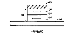
既知の磁気メモリデバイス100の一例が、図1に示される。この図面に示されるように、磁気メモリデバイス100は、2次元のアレイで配列される複数のメモリセルまたはビット102を含む。説明の目的上、図1には比較的少ない数のメモリセル102が示されている。通常は、磁気メモリデバイス100は多数のそのようなセル102を含む。たとえば、デバイス100は、メモリセル102からなる1024×1024のアレイを含むことができる。各メモリセル102は、1ビットの情報、すなわち論理値「1」または論理値「0」を格納するように構成される。
【0004】
図1にさらに示されるように、磁気メモリデバイス100は、メモリセル102に電気的に結合される複数の列導体104および行導体106も含む。具体的には、各メモリセル102は、導体の交点において1つの列導体104と1つの行導体106とに接続される。さらに、磁気メモリデバイス100は、種々の列導体104および行導体106のための切換えをそれぞれ制御する列制御回路108および行制御回路110を含む。
【0005】
図2は、単一のメモリセル102、およびその関連する列導体104および行導体106に対するメモリセルの接続の詳細図を提供する。図2から明らかなように、各メモリセル102は通常、薄い絶縁層204によって分離される2つの磁性層200および202を含む。磁性層のうちの一方(たとえば、下側の磁性層202)は固定された磁気の向きを有し、一方、他方の磁性層(たとえば、上側の磁性層200)は「自由な」磁気の向きを有し、その「自由な」磁気の向きは、固定された磁性層の向きと一致する向きから、固定された磁性層の向きとは反対の向きに比較的容易に切り換えられることができる。メモリセル102の第1の(一致した)状態は「平行」状態と呼ばれ、第2の(反対の)状態は「反平行」状態と呼ばれる。
【0006】
メモリセル102の抵抗に対する本質的に異なる影響に起因して、2つの異なるメモリセル状態を用いてデータを記録することができる。具体的には、メモリセル102は、平行状態のときに比較的小さい抵抗を有し、反平行状態のときに比較的高い抵抗を有する。一例として、平行状態は論理値「1」を表すものとして指定され、一方、反平行状態は論理値「0」を表すものとして指定されることができる。そのような方式では、磁気メモリデバイス100は、選択されたメモリセル102の自由磁性層200の磁気の向きを変化させることにより書込まれ得る。
【0007】
読出しおよび書込み中に任意の所与のメモリセル102の選択を容易にするために、制御回路108および110を用いる。一般に、これらの回路108、110は、選択された導体に電圧を印加するか、または選択された導体に電流を流すために用いられる複数のスイッチ、たとえばトランジスタを含む。図3は、図1および図2に関連して上述したタイプの磁気メモリデバイスのための切換え構成300を示す。図3に示されるように、メモリセルは、列導体304および行導体306に電気的に結合される抵抗302として表される。各導体304、306の両端には、読出しおよび書込み中に種々のメモリセル302を選択するために用いられる読出し/書込みトランジスタ308が存在する。
【0008】
メモリセル302にデータを書き込むために、ある特定のメモリセルに関連する列導体304および行導体306に電流が供給される。たとえば、図3に示される左上のメモリセル302に書込みを行いたい場合には、最も左側にある列導体304と最も上側にある行導体306とに同時に電流が供給される。一例として、各導体の一方の端部に書込み電圧VWRを与え、トランジスタ308を介して各導体の他方の端部をグランドに接続することにより、導体に容易に電流を流すことができる。導体304および306に流れる電流により生成される磁界によって、メモリセル302の自由層(たとえば、図2の層200)の向きが変化し、それによりセルの状態が変更される。
【0009】
一例の読出し方式では、選択されない各メモリセル302に関連する導体304、306に基準電圧VAが与えられ、同時に、選択されたメモリセル302に関連する導体の一方がグランドに接続され、他方には、基準電圧VAに類似した大きさを有する読出し電圧VA’が与えられる。この構成を用いる場合、選択されたメモリセル302に電流が流れ、その際、そのセルの抵抗を求めることができ、それによりそのセルによって格納された論理値を判定することができる。
【0010】
上述の説明から理解されるように、既知の磁気メモリデバイスにおいてメモリセルを選択するために、多数のトランジスタが必要とされる。具体的には、そのデバイスの各列および行導体当たり2つのトランジスタが必要とされる。言い換えると、磁気メモリデバイスの所与の層内におけるn個の導体当たり2n個のトランジスタが必要とされる。既知の磁気メモリデバイス内の導体がメモリセルに電気的に結合されるという理由から、メモリセルの絶縁破壊を避けるために、書込み中に導体に印加される電圧は比較的低く保たなければならない。たとえば、任意のメモリセルの両端の電圧は、約1Vを超えることはできない。メモリセルの両端の電圧を制限するために、トランジスタは比較的大きく、たとえば、読出しのためだけにトランジスタが用いられる場合に必要とされるものよりも100倍大きくしなければならない。したがって、既知の磁気メモリデバイスは、多数の比較的大きなトランジスタを必要とする。これらのトランジスタを設けることにより、磁気メモリデバイスを製作するのに必要な半導体材料(たとえばシリコン)の量、すなわち面積が増加し、それゆえ製造コストが著しく上昇する。
【0011】
【発明が解決しようとする課題】
上述のことから理解されるように、少ない面積しか必要とせず、それにより磁気メモリデバイスによって必要とされる面積を低減する制御回路を含む磁気メモリデバイスが必要とされている。
【0012】
【課題を解決するための手段】
本発明は磁気メモリデバイスに関する。一実施形態では、その磁気メモリデバイスは、複数のメモリセルと、メモリセルに隣接するが、メモリセルから電気的に分離された複数の書込み導体とを含み、書込み導体のうちの少なくとも2つは1つの共有スイッチに接続され、書込み導体は、電流が流れるための経路を提供し、それによりメモリセルの状態を変化させるために用いられる磁界を生成するように構成されている。
【0013】
本発明はさらに、磁気メモリデバイスのメモリセルにデータを書き込むための方法に関する。一実施形態では、その方法は、第1のトランジスタを用いて磁気メモリデバイスの書込み導体の第1の端部に書込み電圧を与えるステップであって、書込み導体がメモリセルから電気的に分離されている、ステップと、磁気メモリデバイスの少なくとも1つの他の書込み導体に接続される第2のトランジスタを用いて、書込み導体の第2の端部をグランドに接続し、第1の電流経路および第1の磁界を形成するステップと、同様にグランドに接続された別個の導体に書込み電圧を与え、第2の電流経路および第2の磁界を形成するステップとを含み、第1および第2の磁界が合わさってメモリセルの状態を変化させる。
【0014】
【発明の実施の形態】
本発明は添付図面を参照することによりさらに深く理解することができる。図面内の構成要素は、必ずしも一定の縮尺で描かれているわけではなく、代わりに本発明の原理を明瞭に示すことに重点が置かれている。
【0015】
上述のように、既知の交点アレイ磁気メモリデバイスは通常、メモリセルアレイにおいて用いられる各導体の各端部に配置された比較的大きなトランジスタを含む。特に、n個の各列および行導体当たり一般に2n個のトランジスタが設けられる。これらのトランジスタは比較的大きな面積を必要とし、したがって過度にデバイスのサイズを大きくし、コストを上昇させる。
【0016】
本明細書では、面積を低減した磁気メモリデバイスが開示され、その磁気メモリデバイスでは、1つまたは複数の付加的な電気的に分離された書込み導体層が設けられる。1つのまたは複数のこのような層を設ける場合、導体のうちの1つまたは複数の層を専用の読出し(すなわちビット)導体として用いて、1つまたは複数の読出し層内のスイッチ(たとえばトランジスタ)の数を、n個の導体当たりn個のスイッチまで減少させることができる。さらに、ビット導体は読出しのためにのみ用いられるので、残りのスイッチのサイズを著しく(たとえば100分の1以下に)減少させることができる。
【0017】
さらに、1つまたは複数の書込み導体層が磁気メモリデバイスのメモリセルに電気的に結合されないという理由から、より高い電圧を用いることもでき、それゆえ1つまたは複数の書込み導体層を切り替えるために、より小型のスイッチを用いることができる。さらに、2つまたはそれより多い書込み導体を1つの共有書込みスイッチを用いて1つの端部において互いに結合することができ、それにより書込み導体のためのスイッチの数をn個の書込み導体当たり(n+1)個のスイッチに減少させることができる。1つまたは複数の書込み導体層を含むことにより、磁気メモリデバイスのコストに増分的に加算されることになるが、スイッチのサイズを減少させることにより得られるコスト削減は、この追加のコストを補って余りある。
【0018】
ここで、類似の参照番号が幾つかの図面を通して対応する部品を示している図面を参照すると、図4および図5は、たとえば磁気ランダムアクセスメモリ(MRAM)デバイスを含むことができる磁気メモリデバイス400を示す。メモリデバイス400は通常、メモリセル402のアレイを含む半導体デバイスとして形成される。図4には限られた数のメモリセル402しか示されないが、デバイスの説明を簡単にするために、デバイス400のメモリセルの描写として数個のセルのみが示されることは理解されたい。
【0019】
メモリセル402に加えて、磁気メモリデバイス400は、複数の列および行導体404および406を含む。以下にさらに詳細に説明されるように、列導体404は読出しのためにのみ用いられ、それゆえ「ビット」線と呼ばれる場合がある。図4に示されるように、アレイの各メモリセル402は、導体の1つの交点において、関連する列導体404および行導体406に電気的に結合される。図5に示されるように、各メモリセル402は、たとえば、第1および第2の磁性層408および410を含み、そのうちの一方は固定された磁性層であり、他方は自由な磁性層である。一例として、上側磁性層408は自由な磁性層を含むことができ、下側磁性層410は固定された磁性層を含むことができる。2つの磁性層408、410は、トンネル障壁として機能する薄い絶縁層412によって分離される。この構成を用いる場合、メモリセル402は、磁気トンネル接合(MTJ)として動作する。本明細書においてMTJ構成が図示および説明されるが、他の構成も実現可能であることは当業者には理解されるであろう。たとえば、メモリセルは、所望に応じて、巨大磁気抵抗(GMR)素子を含むことができる。
【0020】
磁気メモリデバイス400にはさらに、図に示されるように、列導体404に平行に延在するが、列導体404から分離された書込み導体414の層が含まれる。一般に、書込み導体414は、図5に示されるように、薄い絶縁層416によって列導体404から分離される。以下にさらに詳細に説明されるように、書込み導体414は書込み中にのみ用いられる。
【0021】
図6は、図4に示された磁気メモリデバイス400のための切換え構成600を示す。図6では、抵抗602によって、4つのメモリセルが概略的に表される。図4のメモリセル402と同様に、これらのセル602は、磁気メモリデバイス400が含む多数のセルの代表的なものにすぎないことは理解されよう。メモリセル602はそれぞれ、列導体404および行導体406に電気的に結合されるが、各書込み導体414から電気的に分離される。
【0022】
図6にさらに示されるように、各行導体406には、既知の磁気メモリデバイスの場合のように、その各端部に読出し/書込みスイッチ、たとえばトランジスタ604が設けられ、それらの導体がメモリセル602に対する書込みおよび読出しの両方のために使用され得るようにする。これらのトランジスタ604、および以下に説明される他のトランジスタは制御回路(特定せず)の一部を含み、その制御回路によって、導体の切換えを行うことができる。本明細書では「トランジスタ」が明記されているが、当業者であれば、実質的に切換えを行うことができる任意のスイッチまたは他の構成要素を用いることができることは理解されよう。
【0023】
各行導体406当たり2つのトランジスタ604が設けられるが、列導体404(すなわちビット線)は読出しのためにのみ用いられるという理由から、各列導体404についてはただ1つの読出しトランジスタ606しか必要とされない。この構成を用いる場合、n個の列導体404当たりn個の読出しトランジスタ606が存在する。トランジスタの数を削減することに加えて、読出しトランジスタ606は、読出し/書込みトランジスタ604よりも著しく、たとえば100分の1だけ小さくなり、それゆえ必要とされる面積が非常に小さくなる。
【0024】
各書込み導体414には、一端において、書込み中に導体を選択するか、または選択しないために用いられる書込みトランジスタ608が設けられる。書込み導体414がメモリセル602から絶縁されるという理由から、書込み中にメモリセル602に絶縁破壊が生じる危険性はない。したがって、書込み導体414に沿って与えられる電圧は、既知の磁気メモリデバイスにおいて書込みのために一般に使用される電圧よりも大きくすることができる。たとえば、書込み動作中に書込み線414に対して約1.0V〜5.0Vの電圧を供給することができる。この電圧の増加によって、書込みトランジスタ608のサイズを著しく小さくできるとともに、書込み導体414の長さを増すことが可能になる。一例として、書込みトランジスタ608は、読出しトランジスタ606のサイズの約80倍に(読出し/書込みトランジスタ604の場合の100倍と比較して)することができる。
【0025】
上述のトランジスタの数およびサイズの減少は、磁気メモリデバイス400のサイズ、それゆえコストの著しい減少につながる。一端において各書込み導体414を1つの書込み共有トランジスタ610に接続することにより、さらに空間を節約することができる。この構成は、書込み導体414が、メモリセル602の自由磁性層の向きを変化させる電界を生成する電流のための経路としてのみ用いられることから実現可能である。したがって、たとえば、トランジスタ608を用いて、書込み電圧VWRを書込み導体414に与えることができ、書込み共有トランジスタ610を用いて、その導体と他の書込み導体とをグランドに結合し、電流が流れることができる経路を設けることができる。図7は、磁気メモリデバイスから切り離した、この構成の一例を示す。この例に示されるように、種々の導体414は櫛形構成に配列されることができ、各導体は、第1の書込み電圧源700に結合された第1の端部に独自のトランジスタ608を含む。さらに、各導体(たとえば、千個またはそれ以上)は、第2の端部において1つの書込み共有トランジスタ610に結合されることができ、そのトランジスタ610はさらに、第2の書込み電圧源702に接続される。メモリセルに両方の状態を書き込むことできるようにするために(すなわち、導体414に沿って両方向に電流が流れるようにするために)2つの電圧源が用いられることは当業者には理解されよう。図7の構成を用いる場合、書込み導体414当たりのトランジスタの数は、n個の書込み導体当たり(n+1)個まで削減することができ、それにより磁気メモリデバイスのサイズおよびコストをさらに削減することができる。
【0026】
図6に戻って参照すると、メモリセル602にデータを書き込むために、ある特定のメモリセル602に関連した書込み導体414および行導体406に電流が与えられる。たとえば、図6に示される左上のメモリセル602に書込みを行いたい場合には、最も左側の書込み導体414と最も上側の行導体406とに同時に電流が供給される。導体414および406に電流が流れることにより生成される磁界によって、メモリセル602の自由層(たとえば、図5の層408)の向きが反転し、それゆえセルの状態が変化する。
【0027】
メモリセル602は、種々の方法において読み出され得る。一例では、選択されない各メモリセル602に関連した読出し導体404および行導体406に基準電圧VAが与えられ、同時に、選択されたメモリセルに関連した読出し導体のうちの1つがグランドに接続され、他の関連した導体に、基準電圧VAに類似した大きさを有する読出し電圧VA’が与えられる。この切換えによって、選択されたメモリセル602に電流が流れるようになり、抵抗およびそのセルによって格納された論理値を判定できるようになる。一例として、この抵抗はトランスインピーダンス増幅器(図示せず)を用いて求めることができる。
【0028】
図8および図9は、第2の磁気メモリデバイス800を示す。特に、図8はメモリセル802のアレイを示しており、一方、図9は1つのメモリセルと、その関連する導体とを詳細に示す。図4に示される実施形態の場合のように、図8には限られた数のメモリセルしか示されないが、デバイスの説明を簡単にするために、デバイス800の多数のメモリセルの代表的な数個のセルのみが示されることは理解されたい。
【0029】
磁気メモリデバイス400の場合のように、磁気メモリデバイス800は、複数の列および行導体804および806を含む。しかしながら、磁気メモリデバイス800では、列導体804および行導体806の両方が読出しのためにのみ用いられる。図9に示されるように、各メモリセル802は、たとえば、第1および第2の磁性層808および810を含み、その一方は固定されており、他方は自由であり、それらの層は薄い絶縁層812によって分離されている。
【0030】
磁気メモリデバイス800は、デバイス400と同様に、書込み導体814の層を含み、図9に示されるように、それは薄い絶縁層816によって列導体804から分離される。しかしながら、磁気メモリデバイス400とは異なり、磁気メモリデバイス800は、書込み導体818の第2の層を含み、図面に示されるように、それは行導体806と平行に延在し、かつ行導体806から分離される。一例として、この分離は、図9に示されるように、薄い絶縁層820によって提供され得る。大部分の実施形態、特に磁性層808が自由磁性層である実施形態では、行導体806および絶縁層820の厚みは、書込み中に書込み導体818によって生成される磁界を含む磁界が、発生源からの距離の二乗で減少するという理由から、非常に薄く保たれる。
【0031】
図10は、磁気メモリデバイス800のための切換え構成1000を示す。この図面では、抵抗1002によって4つのメモリセルが概略的に表される。これらの各メモリセル1002は、読出しのためだけに用いられる列導体804および行導体806に電気的に結合される。これらの導体804、806はそれぞれ「ビット」線および「ワード」線と呼ばれる場合がある。図10に示されるように、書込み線814および818は、メモリセル1002から電気的に分離される。
【0032】
図4〜図6に関連して説明された先の実施形態の場合のように、各列導体(すなわちビット線)804は、1つの読出しトランジスタ1004しか必要とせず、そのためn個の列導体当たりn個の読出しトランジスタ1004が存在し、各書込み導体814には、一端においてその独自の書込みトランジスタ1006が設けられ、他端において1つの書込み共有トランジスタ1008に結合され、n個の書込み導体当たり(n+1)個の書込みトランジスタが存在する。しかしながら、それに加えて、書込み導体818を設けることに起因して、各行導体(すなわちワード線)806は同様に、1つの読出しトランジスタ1004しか必要とせず、そのためn個の行導体当たりn個の読出しトランジスタ1004が存在し、各書込み導体818には一端においてその独自の書込みトランジスタ1006が設けられ、他端において1つの書込み共有トランジスタ1010に結合されて、行方向に沿ってn個の書込み導体当たり(n+1)個の書込みトランジスタが存在する。
【0033】
読出しおよび書込みは、上述の磁気メモリデバイス400の場合と同様にして達成され得る。しかしながら、図8〜図10のデバイス800の場合、書込みは絶縁された書込み導体814および818を用いて達成されることができ、それらの導体はメモリセルの状態を変化させるために必要とされる磁界を協働して生成し、また全ての読出しは読出し導体804および806を用いて達成される。
【0034】
上述の説明から明らかなように、図8〜図10に示された構成の場合には、さらに大きな空間の節減、それゆえコストの節減を達成することができる。さらに別の導体層を追加するためにコストが加算されるが、制御回路の構成要素を削減することによりもたらされる節減は、余分な導体層を設けることに関連するコストをはるかに上回る。さらに、図8〜図10に示される構成によって、電流拡張効果が回避され、その場合、各書込み導体814、818がメモリセルから電気的に分離されることから、書込み中に選択されないメモリセルで電流が共有される。
【0035】
例示のための先の説明および図面において、本発明の特定の実施形態が詳細に説明されてきたが、特許請求の範囲に記載されるような本発明の範囲から逸脱することなく、その変形および修正を実施できることは当業者であれば理解されよう。
【0036】
【発明の効果】
本発明により、少ない面積しか必要とせず、それにより磁気メモリデバイスによって必要とされる面積を低減する制御回路を含む磁気メモリデバイスを実現することが可能になる。
【図面の簡単な説明】
【図1】既知の磁気メモリデバイスの略平面図である。
【図2】図1の磁気メモリデバイスのメモリセルの側面図である。
【図3】図1の磁気メモリデバイスのための切換え構成を示す電気的接続図である。
【図4】第1の磁気メモリデバイスの概略的な斜視図である。
【図5】図4の磁気メモリデバイスのメモリセルの側面図である。
【図6】図4に示される磁気メモリデバイスの切換え構成を示す電気的接続図である。
【図7】図6の切換え構成において用いられる櫛形導体構成の電気的接続図である。
【図8】第2の磁気メモリデバイスの概略的な斜視図である。
【図9】図8の磁気メモリデバイスのメモリセルの側面図である。
【図10】図8に示される磁気メモリデバイスの切換え構成を示す電気的接続図である。
【符号の説明】
400、800 磁気メモリデバイス
402、602、802、1002 メモリセル
404、804 列導体
406、806 行導体
408、410、808、810 磁性層
414、814、818 書込み導体
412、416、812、816、820 絶縁層
610、1008、1010 書込み共有トランジスタ
1004 読出しトランジスタ
1006 書込みトランジスタ[0001]
TECHNICAL FIELD OF THE INVENTION
The present invention relates to memory devices. More particularly, the present invention relates to magnetic memory devices having a relatively small area.
[0002]
[Prior art]
Magnetic memory, such as magnetic random access memory (MRAM), is a non-volatile, semiconductor-based memory technology that uses magnetism instead of charge to store data bits. In addition to providing non-volatility, magnetic memory devices are very fast and consume low power.
[0003]
One example of a known
[0004]
As further shown in FIG. 1,
[0005]
FIG. 2 provides a detailed view of the connection of a
[0006]
Due to the disparate effects on the resistance of the
[0007]
[0008]
To write data to
[0009]
In one example read scheme, a reference voltage VA is applied to
[0010]
As can be seen from the above description, a large number of transistors are required to select a memory cell in a known magnetic memory device. Specifically, two transistors are required for each column and row conductor of the device. In other words, 2n transistors per n conductors in a given layer of a magnetic memory device are required. Due to the fact that conductors in known magnetic memory devices are electrically coupled to the memory cells, the voltage applied to the conductors during writing must be kept relatively low to avoid breakdown of the memory cells . For example, the voltage across any memory cell cannot exceed about 1V. In order to limit the voltage across the memory cell, the transistor must be relatively large, for example, 100 times larger than would be required if the transistor were used only for reading. Therefore, known magnetic memory devices require a large number of relatively large transistors. The provision of these transistors increases the amount of semiconductor material (eg, silicon) required to fabricate the magnetic memory device, ie, the area, and therefore significantly increases manufacturing costs.
[0011]
[Problems to be solved by the invention]
As can be appreciated from the foregoing, there is a need for a magnetic memory device that includes a control circuit that requires less area, thereby reducing the area required by the magnetic memory device.
[0012]
[Means for Solving the Problems]
The present invention relates to magnetic memory devices. In one embodiment, the magnetic memory device includes a plurality of memory cells and a plurality of write conductors adjacent to, but electrically isolated from, the memory cells, at least two of the write conductors. Connected to one shared switch, the write conductor is configured to provide a path for current to flow, thereby generating a magnetic field that is used to change the state of the memory cell.
[0013]
The invention further relates to a method for writing data to a memory cell of a magnetic memory device. In one embodiment, the method includes applying a write voltage to a first end of a write conductor of a magnetic memory device using a first transistor, wherein the write conductor is electrically isolated from the memory cell. Connecting a second end of the write conductor to ground using a second transistor connected to at least one other write conductor of the magnetic memory device, the first current path and the first current path; And applying a write voltage to a separate conductor also connected to ground to form a second current path and a second magnetic field, wherein the first and second magnetic fields are Together, they change the state of the memory cell.
[0014]
BEST MODE FOR CARRYING OUT THE INVENTION
The invention can be better understood with reference to the following drawings. The components in the figures are not necessarily drawn to scale, emphasis instead being placed upon clearly illustrating the principles of the present invention.
[0015]
As noted above, known cross-array magnetic memory devices typically include relatively large transistors located at each end of each conductor used in the memory cell array. In particular, there are typically 2n transistors per n column and row conductors. These transistors require a relatively large area, and thus excessively increase device size and increase cost.
[0016]
Disclosed herein is a magnetic memory device having a reduced area, wherein the magnetic memory device is provided with one or more additional electrically isolated write conductor layers. Where one or more such layers are provided, one or more of the conductors may be used as dedicated read (ie, bit) conductors and switches (eg, transistors) in one or more of the read layers may be provided. Can be reduced to n switches per n conductors. Further, since the bit conductors are used only for reading, the size of the remaining switches can be significantly reduced (eg, by a factor of less than 100).
[0017]
In addition, higher voltages may be used because one or more write conductor layers are not electrically coupled to the memory cells of the magnetic memory device, and thus may be used to switch one or more write conductor layers. , Smaller switches can be used. Furthermore, two or more write conductors can be coupled together at one end using one shared write switch, thereby reducing the number of switches for the write conductors to (n + 1) ) Switches. The inclusion of one or more write conductor layers will incrementally add to the cost of the magnetic memory device, but the cost savings gained by reducing the size of the switch will offset this additional cost. There are too many.
[0018]
Referring now to the drawings, wherein like reference numerals indicate corresponding parts throughout the several views, FIGS. 4 and 5 illustrate a
[0019]
In addition to
[0020]
[0021]
FIG. 6 shows a switching
[0022]
As further shown in FIG. 6, each
[0023]
Although two
[0024]
Each
[0025]
The reduction in the number and size of the transistors described above leads to a significant reduction in the size of the
[0026]
Referring back to FIG. 6, to write data to
[0027]
[0028]
8 and 9 show a second
[0029]
As with the
[0030]
[0031]
FIG. 10 shows a
[0032]
As in the previous embodiment described in connection with FIGS. 4-6, each column conductor (ie, bit line) 804 requires only one
[0033]
Reading and writing can be accomplished in a manner similar to that of the
[0034]
As is clear from the above description, the configurations shown in FIGS. 8 to 10 can achieve a larger space saving and therefore a cost saving. Although the costs are added to add yet another conductor layer, the savings provided by reducing the components of the control circuitry far exceed the costs associated with providing extra conductor layers. In addition, the configuration shown in FIGS. 8-10 avoids the current spreading effect, in which case each
[0035]
Although specific embodiments of the present invention have been described in detail in the foregoing description and drawings for illustration, modifications and variations thereof may be made without departing from the scope of the present invention as set forth in the claims below. Those skilled in the art will appreciate that modifications can be made.
[0036]
【The invention's effect】
The present invention makes it possible to realize a magnetic memory device that requires a small area and thus includes a control circuit that reduces the area required by the magnetic memory device.
[Brief description of the drawings]
FIG. 1 is a schematic plan view of a known magnetic memory device.
FIG. 2 is a side view of a memory cell of the magnetic memory device of FIG. 1;
FIG. 3 is an electrical connection diagram illustrating a switching configuration for the magnetic memory device of FIG. 1;
FIG. 4 is a schematic perspective view of a first magnetic memory device.
FIG. 5 is a side view of a memory cell of the magnetic memory device of FIG. 4;
6 is an electrical connection diagram showing a switching configuration of the magnetic memory device shown in FIG.
FIG. 7 is an electrical connection diagram of a comb-shaped conductor configuration used in the switching configuration of FIG. 6;
FIG. 8 is a schematic perspective view of a second magnetic memory device.
FIG. 9 is a side view of a memory cell of the magnetic memory device of FIG. 8;
FIG. 10 is an electrical connection diagram showing a switching configuration of the magnetic memory device shown in FIG. 8;
[Explanation of symbols]
400, 800
Claims (10)
複数のメモリセル(602)と、および
前記メモリセルに隣接するが、前記メモリセルから電気的に分離される複数の書込み導体(414)とを備え、前記書込み導体のうちの少なくとも2つが、1つの共有スイッチ(610)に接続され、前記書込み導体は、電流が流れるための経路を提供し、それにより前記メモリセルの状態を変化させるために用いられる磁界を生成するように構成されている、磁気メモリデバイス(600)。A magnetic memory device (600), comprising:
A plurality of memory cells (602); and a plurality of write conductors (414) adjacent to the memory cells but electrically isolated from the memory cells, wherein at least two of the write conductors are Connected to one shared switch (610), the write conductor is configured to provide a path for current to flow, thereby creating a magnetic field used to change the state of the memory cell; Magnetic memory device (600).
2次元のアレイに配列された複数のメモリセル(602)と、
前記メモリセルのうちの第1の側にある前記メモリセルに電気的に結合され、書込み中に前記メモリセルのための磁界を与え、読出し中に前記メモリセルに電流を与えるように構成されている、複数の読出し/書込み導体(406)と、
前記メモリセルのうちの第2の側にある前記メモリセルに電気的に結合され、読出し中に前記メモリセルに電流を与えるように構成されている、複数の読出し導体(404)と、および
前記読出し導体に隣接し、前記メモリセルから電気的に分離された複数の書込み導体(414)とを備え、前記書込み導体のうちの少なくとも2つが1つの共有トランジスタ(610)に接続され、前記書込み導体が書込み中に前記メモリセルのための磁界を生成するように構成されている、磁気メモリデバイス(600)。A magnetic memory device (600), comprising:
A plurality of memory cells (602) arranged in a two-dimensional array;
Electrically coupled to the memory cells on a first side of the memory cells and configured to provide a magnetic field for the memory cells during writing and to provide current to the memory cells during reading; A plurality of read / write conductors (406);
A plurality of read conductors (404) electrically coupled to the memory cells on a second one of the memory cells and configured to provide current to the memory cells during reading; and A plurality of write conductors adjacent to a read conductor and electrically isolated from the memory cell, at least two of the write conductors being connected to one shared transistor; A magnetic memory device (600), wherein the device is configured to generate a magnetic field for the memory cell during writing.
2次元のアレイに配列された複数のメモリセル(1002)と、
前記メモリセルのうちの第1の側にある前記メモリセルに電気的に結合され、前記メモリセルに読出し電流を与えるように構成されている、第1の層の読出し導体(804)と、
前記第1の層の読出し導体に隣接し、前記メモリセルから電気的に分離された第1の層の書込み導体(814)であって、その書込み導体のうちの少なくとも2つが第1の共有トランジスタ(1008)に接続され、前記書込み導体が前記メモリセルのための磁界を生成するように構成されている、第1の層の書込み導体と、
前記メモリセルのうちの第2の側にある前記メモリセルに電気的に結合された第2の層の読出し導体(806)と、および
前記第2の層の読出し導体に隣接し、前記メモリセルから電気的に分離された第2の層の書込み導体(818)とを備え、その第2の層の書込み導体のうちの少なくとも2つが第2の共有トランジスタ(1010)に接続され、前記第2の層の書込み導体が前記メモリセルのための磁界を生成するように構成されている、磁気メモリデバイス(1000)。A magnetic memory device (1000),
A plurality of memory cells (1002) arranged in a two-dimensional array;
A first layer read conductor (804) electrically coupled to the memory cells on a first side of the memory cells and configured to provide a read current to the memory cells;
A first layer write conductor (814) adjacent the first layer read conductor and electrically isolated from the memory cells, wherein at least two of the write conductors are first shared transistors A first layer write conductor connected to (1008), wherein the write conductor is configured to generate a magnetic field for the memory cell;
A second layer read conductor (806) electrically coupled to the memory cell on a second one of the memory cells; and the memory cell adjacent to the second layer read conductor. A second layer write conductor (818) electrically isolated from a second shared transistor (1010), wherein the second layer write conductor is connected to a second shared transistor (1010). The magnetic memory device (1000), wherein the write conductors of the layers are configured to generate a magnetic field for the memory cell.
第1のトランジスタを用いて前記磁気メモリデバイスの書込み導体の第1の端部に書込み電圧を与えるステップであって、前記書込み導体が前記メモリセルから電気的に分離されている、ステップと、
前記書込み導体の第2の端部を、前記磁気メモリデバイスの少なくとも1つの他の書込み導体に接続された第2のトランジスタを用いてグランドに接続し、第1の電流経路および第1の磁界を形成するステップと、および
第2の電流経路および第2の磁界を形成するために、グランドに接続された別個の導体にも書込み電圧を与えるステップとを含み、
前記第1および前記第2の磁界が合わさって前記メモリセルの状態を変化させる、方法。A method for writing data to a memory cell of a magnetic memory device, comprising:
Applying a write voltage to a first end of a write conductor of the magnetic memory device using a first transistor, wherein the write conductor is electrically isolated from the memory cell;
A second end of the write conductor is connected to ground using a second transistor connected to at least one other write conductor of the magnetic memory device, and a first current path and a first magnetic field are coupled. Forming, and applying a write voltage also to a separate conductor connected to ground to form a second current path and a second magnetic field,
A method wherein the first and second magnetic fields combine to change a state of the memory cell.
Applications Claiming Priority (1)
| Application Number | Priority Date | Filing Date | Title |
|---|---|---|---|
| US10/147,597 US6781910B2 (en) | 2002-05-17 | 2002-05-17 | Small area magnetic memory devices |
Publications (2)
| Publication Number | Publication Date |
|---|---|
| JP2004005965A true JP2004005965A (en) | 2004-01-08 |
| JP2004005965A5 JP2004005965A5 (en) | 2006-06-22 |
Family
ID=29419048
Family Applications (1)
| Application Number | Title | Priority Date | Filing Date |
|---|---|---|---|
| JP2003131176A Pending JP2004005965A (en) | 2002-05-17 | 2003-05-09 | Magnetic memory device of small area |
Country Status (3)
| Country | Link |
|---|---|
| US (1) | US6781910B2 (en) |
| JP (1) | JP2004005965A (en) |
| DE (1) | DE10314812A1 (en) |
Families Citing this family (79)
| Publication number | Priority date | Publication date | Assignee | Title |
|---|---|---|---|---|
| US6991029B2 (en) * | 2003-06-06 | 2006-01-31 | Orfield Laboratories, Inc. | Architectural dynamic control: intelligent environmental control and feedback system for architectural settings including offices |
| US6865105B1 (en) * | 2003-09-22 | 2005-03-08 | Hewlett-Packard Development Company, L.P. | Thermal-assisted switching array configuration for MRAM |
| US7366009B2 (en) * | 2004-01-10 | 2008-04-29 | Honeywell International Inc. | Separate write and read access architecture for a magnetic tunnel junction |
| US8650352B2 (en) | 2007-09-20 | 2014-02-11 | Densbits Technologies Ltd. | Systems and methods for determining logical values of coupled flash memory cells |
| WO2009095902A2 (en) | 2008-01-31 | 2009-08-06 | Densbits Technologies Ltd. | Systems and methods for handling immediate data errors in flash memory |
| US8694715B2 (en) | 2007-10-22 | 2014-04-08 | Densbits Technologies Ltd. | Methods for adaptively programming flash memory devices and flash memory systems incorporating same |
| US8443242B2 (en) * | 2007-10-25 | 2013-05-14 | Densbits Technologies Ltd. | Systems and methods for multiple coding rates in flash devices |
| WO2009072105A2 (en) | 2007-12-05 | 2009-06-11 | Densbits Technologies Ltd. | A low power chien-search based bch/rs decoding system for flash memory, mobile communications devices and other applications |
| US8321625B2 (en) | 2007-12-05 | 2012-11-27 | Densbits Technologies Ltd. | Flash memory device with physical cell value deterioration accommodation and methods useful in conjunction therewith |
| WO2009072103A2 (en) | 2007-12-05 | 2009-06-11 | Densbits Technologies Ltd. | Flash memory apparatus and methods using a plurality of decoding stages including optional use of concatenated bch codes and/or designation of 'first below' cells |
| US8276051B2 (en) | 2007-12-12 | 2012-09-25 | Densbits Technologies Ltd. | Chien-search system employing a clock-gating scheme to save power for error correction decoder and other applications |
| US8359516B2 (en) | 2007-12-12 | 2013-01-22 | Densbits Technologies Ltd. | Systems and methods for error correction and decoding on multi-level physical media |
| US8327246B2 (en) | 2007-12-18 | 2012-12-04 | Densbits Technologies Ltd. | Apparatus for coding at a plurality of rates in multi-level flash memory systems, and methods useful in conjunction therewith |
| WO2009118720A2 (en) | 2008-03-25 | 2009-10-01 | Densbits Technologies Ltd. | Apparatus and methods for hardware-efficient unbiased rounding |
| US8332725B2 (en) | 2008-08-20 | 2012-12-11 | Densbits Technologies Ltd. | Reprogramming non volatile memory portions |
| US8819385B2 (en) | 2009-04-06 | 2014-08-26 | Densbits Technologies Ltd. | Device and method for managing a flash memory |
| US8458574B2 (en) | 2009-04-06 | 2013-06-04 | Densbits Technologies Ltd. | Compact chien-search based decoding apparatus and method |
| US8566510B2 (en) | 2009-05-12 | 2013-10-22 | Densbits Technologies Ltd. | Systems and method for flash memory management |
| US9330767B1 (en) | 2009-08-26 | 2016-05-03 | Avago Technologies General Ip (Singapore) Pte. Ltd. | Flash memory module and method for programming a page of flash memory cells |
| US8868821B2 (en) | 2009-08-26 | 2014-10-21 | Densbits Technologies Ltd. | Systems and methods for pre-equalization and code design for a flash memory |
| US8995197B1 (en) | 2009-08-26 | 2015-03-31 | Densbits Technologies Ltd. | System and methods for dynamic erase and program control for flash memory device memories |
| US8305812B2 (en) | 2009-08-26 | 2012-11-06 | Densbits Technologies Ltd. | Flash memory module and method for programming a page of flash memory cells |
| US8730729B2 (en) | 2009-10-15 | 2014-05-20 | Densbits Technologies Ltd. | Systems and methods for averaging error rates in non-volatile devices and storage systems |
| US8724387B2 (en) | 2009-10-22 | 2014-05-13 | Densbits Technologies Ltd. | Method, system, and computer readable medium for reading and programming flash memory cells using multiple bias voltages |
| US8626988B2 (en) | 2009-11-19 | 2014-01-07 | Densbits Technologies Ltd. | System and method for uncoded bit error rate equalization via interleaving |
| US9037777B2 (en) | 2009-12-22 | 2015-05-19 | Densbits Technologies Ltd. | Device, system, and method for reducing program/read disturb in flash arrays |
| US8607124B2 (en) | 2009-12-24 | 2013-12-10 | Densbits Technologies Ltd. | System and method for setting a flash memory cell read threshold |
| US8341502B2 (en) | 2010-02-28 | 2012-12-25 | Densbits Technologies Ltd. | System and method for multi-dimensional decoding |
| US8527840B2 (en) | 2010-04-06 | 2013-09-03 | Densbits Technologies Ltd. | System and method for restoring damaged data programmed on a flash device |
| US9104610B2 (en) | 2010-04-06 | 2015-08-11 | Densbits Technologies Ltd. | Method, system and medium for analog encryption in a flash memory |
| US8745317B2 (en) | 2010-04-07 | 2014-06-03 | Densbits Technologies Ltd. | System and method for storing information in a multi-level cell memory |
| US9021177B2 (en) | 2010-04-29 | 2015-04-28 | Densbits Technologies Ltd. | System and method for allocating and using spare blocks in a flash memory |
| US8510639B2 (en) | 2010-07-01 | 2013-08-13 | Densbits Technologies Ltd. | System and method for multi-dimensional encoding and decoding |
| US8539311B2 (en) | 2010-07-01 | 2013-09-17 | Densbits Technologies Ltd. | System and method for data recovery in multi-level cell memories |
| US8467249B2 (en) | 2010-07-06 | 2013-06-18 | Densbits Technologies Ltd. | Systems and methods for storing, retrieving, and adjusting read thresholds in flash memory storage system |
| US8964464B2 (en) | 2010-08-24 | 2015-02-24 | Densbits Technologies Ltd. | System and method for accelerated sampling |
| US8508995B2 (en) | 2010-09-15 | 2013-08-13 | Densbits Technologies Ltd. | System and method for adjusting read voltage thresholds in memories |
| US9063878B2 (en) | 2010-11-03 | 2015-06-23 | Densbits Technologies Ltd. | Method, system and computer readable medium for copy back |
| US8850100B2 (en) | 2010-12-07 | 2014-09-30 | Densbits Technologies Ltd. | Interleaving codeword portions between multiple planes and/or dies of a flash memory device |
| US10079068B2 (en) | 2011-02-23 | 2018-09-18 | Avago Technologies General Ip (Singapore) Pte. Ltd. | Devices and method for wear estimation based memory management |
| US8693258B2 (en) | 2011-03-17 | 2014-04-08 | Densbits Technologies Ltd. | Obtaining soft information using a hard interface |
| US8990665B1 (en) | 2011-04-06 | 2015-03-24 | Densbits Technologies Ltd. | System, method and computer program product for joint search of a read threshold and soft decoding |
| US9195592B1 (en) | 2011-05-12 | 2015-11-24 | Densbits Technologies Ltd. | Advanced management of a non-volatile memory |
| US9372792B1 (en) | 2011-05-12 | 2016-06-21 | Avago Technologies General Ip (Singapore) Pte. Ltd. | Advanced management of a non-volatile memory |
| US9501392B1 (en) | 2011-05-12 | 2016-11-22 | Avago Technologies General Ip (Singapore) Pte. Ltd. | Management of a non-volatile memory module |
| US9396106B2 (en) | 2011-05-12 | 2016-07-19 | Avago Technologies General Ip (Singapore) Pte. Ltd. | Advanced management of a non-volatile memory |
| US9110785B1 (en) | 2011-05-12 | 2015-08-18 | Densbits Technologies Ltd. | Ordered merge of data sectors that belong to memory space portions |
| US8996790B1 (en) | 2011-05-12 | 2015-03-31 | Densbits Technologies Ltd. | System and method for flash memory management |
| US8667211B2 (en) | 2011-06-01 | 2014-03-04 | Densbits Technologies Ltd. | System and method for managing a non-volatile memory |
| US8588003B1 (en) | 2011-08-01 | 2013-11-19 | Densbits Technologies Ltd. | System, method and computer program product for programming and for recovering from a power failure |
| US8553468B2 (en) | 2011-09-21 | 2013-10-08 | Densbits Technologies Ltd. | System and method for managing erase operations in a non-volatile memory |
| US8947941B2 (en) | 2012-02-09 | 2015-02-03 | Densbits Technologies Ltd. | State responsive operations relating to flash memory cells |
| US8996788B2 (en) | 2012-02-09 | 2015-03-31 | Densbits Technologies Ltd. | Configurable flash interface |
| US20130258750A1 (en) * | 2012-03-30 | 2013-10-03 | International Business Machines Corporation | Dual-cell mtj structure with individual access and logical combination ability |
| US8996793B1 (en) | 2012-04-24 | 2015-03-31 | Densbits Technologies Ltd. | System, method and computer readable medium for generating soft information |
| US9196337B2 (en) | 2012-04-25 | 2015-11-24 | Qualcomm Incorporated | Low sensing current non-volatile flip-flop |
| US8838937B1 (en) | 2012-05-23 | 2014-09-16 | Densbits Technologies Ltd. | Methods, systems and computer readable medium for writing and reading data |
| US8879325B1 (en) | 2012-05-30 | 2014-11-04 | Densbits Technologies Ltd. | System, method and computer program product for processing read threshold information and for reading a flash memory module |
| US9921954B1 (en) | 2012-08-27 | 2018-03-20 | Avago Technologies General Ip (Singapore) Pte. Ltd. | Method and system for split flash memory management between host and storage controller |
| US9368225B1 (en) | 2012-11-21 | 2016-06-14 | Avago Technologies General Ip (Singapore) Pte. Ltd. | Determining read thresholds based upon read error direction statistics |
| US9069659B1 (en) | 2013-01-03 | 2015-06-30 | Densbits Technologies Ltd. | Read threshold determination using reference read threshold |
| US9136876B1 (en) | 2013-06-13 | 2015-09-15 | Densbits Technologies Ltd. | Size limited multi-dimensional decoding |
| US9413491B1 (en) | 2013-10-08 | 2016-08-09 | Avago Technologies General Ip (Singapore) Pte. Ltd. | System and method for multiple dimension decoding and encoding a message |
| US9786388B1 (en) | 2013-10-09 | 2017-10-10 | Avago Technologies General Ip (Singapore) Pte. Ltd. | Detecting and managing bad columns |
| US9397706B1 (en) | 2013-10-09 | 2016-07-19 | Avago Technologies General Ip (Singapore) Pte. Ltd. | System and method for irregular multiple dimension decoding and encoding |
| US9348694B1 (en) | 2013-10-09 | 2016-05-24 | Avago Technologies General Ip (Singapore) Pte. Ltd. | Detecting and managing bad columns |
| US9536612B1 (en) | 2014-01-23 | 2017-01-03 | Avago Technologies General Ip (Singapore) Pte. Ltd | Digital signaling processing for three dimensional flash memory arrays |
| US10120792B1 (en) | 2014-01-29 | 2018-11-06 | Avago Technologies General Ip (Singapore) Pte. Ltd. | Programming an embedded flash storage device |
| KR20160145002A (en) | 2014-04-10 | 2016-12-19 | 휴렛 팩커드 엔터프라이즈 디벨롭먼트 엘피 | 1-selector n-resistor memristive devices |
| US9542262B1 (en) | 2014-05-29 | 2017-01-10 | Avago Technologies General Ip (Singapore) Pte. Ltd. | Error correction |
| US9892033B1 (en) | 2014-06-24 | 2018-02-13 | Avago Technologies General Ip (Singapore) Pte. Ltd. | Management of memory units |
| US9972393B1 (en) | 2014-07-03 | 2018-05-15 | Avago Technologies General Ip (Singapore) Pte. Ltd. | Accelerating programming of a flash memory module |
| US9584159B1 (en) | 2014-07-03 | 2017-02-28 | Avago Technologies General Ip (Singapore) Pte. Ltd. | Interleaved encoding |
| US9449702B1 (en) | 2014-07-08 | 2016-09-20 | Avago Technologies General Ip (Singapore) Pte. Ltd. | Power management |
| US9524211B1 (en) | 2014-11-18 | 2016-12-20 | Avago Technologies General Ip (Singapore) Pte. Ltd. | Codeword management |
| US10305515B1 (en) | 2015-02-02 | 2019-05-28 | Avago Technologies International Sales Pte. Limited | System and method for encoding using multiple linear feedback shift registers |
| US10628255B1 (en) | 2015-06-11 | 2020-04-21 | Avago Technologies International Sales Pte. Limited | Multi-dimensional decoding |
| US9851921B1 (en) | 2015-07-05 | 2017-12-26 | Avago Technologies General Ip (Singapore) Pte. Ltd. | Flash memory chip processing |
| US9954558B1 (en) | 2016-03-03 | 2018-04-24 | Avago Technologies General Ip (Singapore) Pte. Ltd. | Fast decoding of data stored in a flash memory |
Family Cites Families (7)
| Publication number | Priority date | Publication date | Assignee | Title |
|---|---|---|---|---|
| US6097626A (en) * | 1999-07-28 | 2000-08-01 | Hewlett-Packard Company | MRAM device using magnetic field bias to suppress inadvertent switching of half-selected memory cells |
| US6473336B2 (en) * | 1999-12-16 | 2002-10-29 | Kabushiki Kaisha Toshiba | Magnetic memory device |
| US6215707B1 (en) * | 2000-04-10 | 2001-04-10 | Motorola Inc. | Charge conserving write method and system for an MRAM |
| US6587370B2 (en) * | 2000-11-01 | 2003-07-01 | Canon Kabushiki Kaisha | Magnetic memory and information recording and reproducing method therefor |
| JP4712204B2 (en) * | 2001-03-05 | 2011-06-29 | ルネサスエレクトロニクス株式会社 | Storage device |
| US6490217B1 (en) * | 2001-05-23 | 2002-12-03 | International Business Machines Corporation | Select line architecture for magnetic random access memories |
| US6678189B2 (en) * | 2002-02-25 | 2004-01-13 | Hewlett-Packard Development Company, L.P. | Method and system for performing equipotential sensing across a memory array to eliminate leakage currents |
-
2002
- 2002-05-17 US US10/147,597 patent/US6781910B2/en not_active Expired - Lifetime
-
2003
- 2003-04-01 DE DE10314812A patent/DE10314812A1/en not_active Withdrawn
- 2003-05-09 JP JP2003131176A patent/JP2004005965A/en active Pending
Also Published As
| Publication number | Publication date |
|---|---|
| US20030214838A1 (en) | 2003-11-20 |
| DE10314812A1 (en) | 2003-12-04 |
| US6781910B2 (en) | 2004-08-24 |
Similar Documents
| Publication | Publication Date | Title |
|---|---|---|
| JP2004005965A (en) | Magnetic memory device of small area | |
| US7411815B2 (en) | Memory write circuit | |
| JP5019681B2 (en) | Thin film magnetic memory device | |
| US7180770B2 (en) | Series diode thermally assisted MRAM | |
| JP3906212B2 (en) | Magnetic random access memory | |
| US7196957B2 (en) | Magnetic memory structure using heater lines to assist in writing operations | |
| KR20080053280A (en) | Passive elements in mram embedded integrated circuits | |
| TW200303028A (en) | Magnetoresistive random access memory (MRAM ) cross-point array with reduced parasitic effects | |
| JP2002050173A (en) | Non-volatile storage device | |
| KR100898040B1 (en) | Mram device including offset conductors | |
| US7471549B2 (en) | Semiconductor memory device | |
| US8830734B2 (en) | Using a nearby cell to provide field assisted switching in a magnetic memory array | |
| US6925003B2 (en) | Magnetic memory cell structure | |
| JP2007213639A (en) | Nonvolatile semiconductor memory | |
| JP3844117B2 (en) | Memory cell, memory circuit block, data writing method and data reading method | |
| US7269060B2 (en) | Magnetic random access memory | |
| JP2004006861A (en) | Magnetic random access memory whose parasitic current is reduced | |
| EP1662510B1 (en) | Arrangement of write lines in an MRAM device | |
| US6507513B1 (en) | Using delayed electrical pulses with magneto-resistive devices | |
| US7986548B2 (en) | Current re-routing scheme for serial-programmed MRAM | |
| US6944053B2 (en) | Magnetic memory with structure providing reduced coercivity | |
| JP5300959B2 (en) | Thin film magnetic memory device | |
| JP5140859B2 (en) | Semiconductor device | |
| US10056128B2 (en) | Semiconductor storage device | |
| US20070171703A1 (en) | Current source of magnetic random access memory |
Legal Events
| Date | Code | Title | Description |
|---|---|---|---|
| A521 | Request for written amendment filed |
Free format text: JAPANESE INTERMEDIATE CODE: A523 Effective date: 20060501 |
|
| A621 | Written request for application examination |
Free format text: JAPANESE INTERMEDIATE CODE: A621 Effective date: 20060501 |
|
| A711 | Notification of change in applicant |
Free format text: JAPANESE INTERMEDIATE CODE: A711 Effective date: 20070706 |
|
| A977 | Report on retrieval |
Free format text: JAPANESE INTERMEDIATE CODE: A971007 Effective date: 20090513 |
|
| A131 | Notification of reasons for refusal |
Free format text: JAPANESE INTERMEDIATE CODE: A131 Effective date: 20090519 |
|
| A601 | Written request for extension of time |
Free format text: JAPANESE INTERMEDIATE CODE: A601 Effective date: 20090819 |
|
| A602 | Written permission of extension of time |
Free format text: JAPANESE INTERMEDIATE CODE: A602 Effective date: 20090824 |
|
| A601 | Written request for extension of time |
Free format text: JAPANESE INTERMEDIATE CODE: A601 Effective date: 20090918 |
|
| A602 | Written permission of extension of time |
Free format text: JAPANESE INTERMEDIATE CODE: A602 Effective date: 20090928 |
|
| A521 | Request for written amendment filed |
Free format text: JAPANESE INTERMEDIATE CODE: A523 Effective date: 20091008 |
|
| A02 | Decision of refusal |
Free format text: JAPANESE INTERMEDIATE CODE: A02 Effective date: 20091104 |