JP2002287376A5 - - Google Patents
Download PDFInfo
- Publication number
- JP2002287376A5 JP2002287376A5 JP2001086757A JP2001086757A JP2002287376A5 JP 2002287376 A5 JP2002287376 A5 JP 2002287376A5 JP 2001086757 A JP2001086757 A JP 2001086757A JP 2001086757 A JP2001086757 A JP 2001086757A JP 2002287376 A5 JP2002287376 A5 JP 2002287376A5
- Authority
- JP
- Japan
- Prior art keywords
- film
- magnetic
- insulating film
- insulating
- photoresist
- Prior art date
- Legal status (The legal status is an assumption and is not a legal conclusion. Google has not performed a legal analysis and makes no representation as to the accuracy of the status listed.)
- Granted
Links
Images


Description
【0030】
【発明の実施の形態】
以下、本発明を、図面と関連させながら発明の実施の形態に基づいて詳細に説明する。ここに示した構成は、実施態様の一例を示すものであり特許範囲を規定するものでない。
図1〜9は、本発明の薄膜磁気ヘッドの製造方法を用いて薄膜磁気ヘッドを作製する場合の一例を示す工程図である。なお、図1〜9においては、本発明の特徴を明確にすべく、各部分の大きさについては実際のものと異なるようにして描いている。[0030]
BEST MODE FOR CARRYING OUT THE INVENTION
Hereinafter, the present invention will be described in detail based on embodiments of the invention with reference to the drawings. The configuration shown here is an example of the embodiment and does not define the scope of the patent.
1 to 9 are process diagrams showing an example of the case of producing a thin film magnetic head using the method of manufacturing a thin film magnetic head of the present invention. In addition, in FIGS. 1-9, in order to clarify the characteristic of this invention, it has drawn so that the magnitude | size of each part may differ from an actual thing.
【0031】
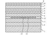
最初に図1に示すように、AlTiCなどからなる基板1上に絶縁膜2、下部シールド膜11、絶縁膜12を形成するとともに、読み取り素子としてもMR素子13及びMRリード14を絶縁膜12に埋設するようにして形成する。次いで、絶縁膜12上に第1の磁性膜3、及びギャップ膜4を形成する。絶縁膜2は、Al2O3、SiO2などの絶縁性材料からスパッタリング法などを用いて、厚さ4〜7μmに形成する。第1の磁性膜3は、NiFe、CoFe、及びCoNiFeなどの軟磁性材料から同じくスパッタリング法などを用いて、厚さ0.5〜4μmに形成する。[0031]
First, as shown in FIG. 1, the
【符号の説明】
1 基板
2 絶縁膜
3 第1の磁性膜
4 ギャップ膜
5 電極膜
6 保護電極膜
7 第1のフォトレジスト層
8 中間層
9 第2のフォトレジスト層
10 第2の磁性膜
11 下部シールド膜
12 絶縁膜
13 MR素子
14 MRリード
17 フォトレジストフレーム
18 エッチング用マスク
19 フォトレジストパターン[Description of the code]
Priority Applications (2)
| Application Number | Priority Date | Filing Date | Title |
|---|---|---|---|
| JP2001086757A JP4176322B2 (en) | 2001-03-26 | 2001-03-26 | Thin film forming method and thin film magnetic head manufacturing method |
| US10/097,625 US6935014B2 (en) | 2001-03-26 | 2002-03-15 | Method for fabricating a thin film magnetic head |
Applications Claiming Priority (1)
| Application Number | Priority Date | Filing Date | Title |
|---|---|---|---|
| JP2001086757A JP4176322B2 (en) | 2001-03-26 | 2001-03-26 | Thin film forming method and thin film magnetic head manufacturing method |
Publications (3)
| Publication Number | Publication Date |
|---|---|
| JP2002287376A JP2002287376A (en) | 2002-10-03 |
| JP2002287376A5 true JP2002287376A5 (en) | 2004-08-19 |
| JP4176322B2 JP4176322B2 (en) | 2008-11-05 |
Family
ID=18942087
Family Applications (1)
| Application Number | Title | Priority Date | Filing Date |
|---|---|---|---|
| JP2001086757A Expired - Fee Related JP4176322B2 (en) | 2001-03-26 | 2001-03-26 | Thin film forming method and thin film magnetic head manufacturing method |
Country Status (2)
| Country | Link |
|---|---|
| US (1) | US6935014B2 (en) |
| JP (1) | JP4176322B2 (en) |
Families Citing this family (5)
| Publication number | Priority date | Publication date | Assignee | Title |
|---|---|---|---|---|
| JP3886802B2 (en) * | 2001-03-30 | 2007-02-28 | 株式会社東芝 | Magnetic patterning method, magnetic recording medium, magnetic random access memory |
| JP2005018836A (en) * | 2003-06-23 | 2005-01-20 | Hitachi Ltd | Magnetic head and method for manufacturing the same |
| JP5554466B2 (en) * | 2004-03-01 | 2014-07-23 | 味の素株式会社 | Anti-human TNF-α antibody activity decrease inhibitor |
| JP2009266340A (en) * | 2008-04-28 | 2009-11-12 | Fujitsu Ltd | Method of manufacturing vertical magnetic head |
| JP2012099589A (en) * | 2010-11-01 | 2012-05-24 | Hitachi High-Technologies Corp | Plasma processing apparatus |
Family Cites Families (6)
| Publication number | Priority date | Publication date | Assignee | Title |
|---|---|---|---|---|
| US5438747A (en) * | 1994-03-09 | 1995-08-08 | International Business Machines Corporation | Method of making a thin film merged MR head with aligned pole tips |
| US5665251A (en) * | 1994-11-23 | 1997-09-09 | International Business Machines Corporation | RIE image transfer process for plating |
| JP3790347B2 (en) * | 1997-11-26 | 2006-06-28 | Tdk株式会社 | Manufacturing method of thin film magnetic head |
| JP3503874B2 (en) * | 1998-09-29 | 2004-03-08 | Tdk株式会社 | Method for manufacturing thin-film magnetic head |
| US6156487A (en) * | 1998-10-23 | 2000-12-05 | Matsushita-Kotobuki Electronics Industries, Ltd. | Top surface imaging technique for top pole tip width control in magnetoresistive read/write head processing |
| US6539610B1 (en) * | 2000-07-14 | 2003-04-01 | International Business Machines Corporation | Method for manufacturing a magnetic write head |
-
2001
- 2001-03-26 JP JP2001086757A patent/JP4176322B2/en not_active Expired - Fee Related
-
2002
- 2002-03-15 US US10/097,625 patent/US6935014B2/en not_active Expired - Lifetime
Similar Documents
| Publication | Publication Date | Title |
|---|---|---|
| JP2000163713A (en) | Forming method of upper magnetic pole layer of thin film magnetic head, forming method of fine block pattern of high aspect ratio on bottom of step on surface having steps, and thin film magnetic head | |
| JPS5971115A (en) | Thin film head for vertical magnetic recording and reproduction | |
| JP2006179051A (en) | Magnetoresistive sensor and its manufacturing method | |
| JP2004363157A (en) | Thin film magnetic sensor and its manufacturing method | |
| US6373657B1 (en) | Thin film magnetic head with magnetic film offsets at forefront surfaces thereof | |
| JP2002287376A5 (en) | ||
| JP2000048318A (en) | Thin film magnetic head and its production | |
| US20080304179A1 (en) | Perpendicular magnetic recording head and method of manufacturing same | |
| JP2001076314A (en) | Manufacture of thin film magnetic head | |
| US6558516B1 (en) | Method of frame plating and method of forming magnetic pole of thin-film magnetic head | |
| US6399285B1 (en) | Method for forming a thin film and for manufacturing a thin film | |
| JPH064829A (en) | Thin-film magnetic head and its production | |
| US7343669B2 (en) | Method of manufacturing a thin film magnetic head | |
| JP2009223980A (en) | Method of manufacturing thin-film magnetic head | |
| JP2007019288A (en) | Thin film forming method and manufacturing method of micro-device | |
| JP3919926B2 (en) | Manufacturing method of thin film magnetic head | |
| JPH08263807A (en) | Formation of magnetic pole of thin-film magnetic head | |
| JPH06338030A (en) | Production of horizontal thin film magnetic head | |
| FR2780196B1 (en) | METHOD FOR PRODUCING A MAGNETIC RECORDING / READING HEAD AND APPLICATION TO A MATRIX HEAD | |
| JP2020165817A (en) | Magnetic sensor and manufacturing method therefor | |
| US20010036601A1 (en) | Masking frame plating method for forming masking frame plated layer | |
| JP2833583B2 (en) | Patterning method for magnetoresistive element | |
| JP3164050B2 (en) | Manufacturing method of magnetoresistive composite head | |
| US20030067713A1 (en) | Novel photoresist material to achieve hardbake resist shape control | |
| JPH1074307A (en) | Production of composite magnetic head |