EP4583672A2 - Light emitting device including a lead frame and an insulating material cross reference to related applications - Google Patents
Light emitting device including a lead frame and an insulating material cross reference to related applications Download PDFInfo
- Publication number
- EP4583672A2 EP4583672A2 EP25169804.9A EP25169804A EP4583672A2 EP 4583672 A2 EP4583672 A2 EP 4583672A2 EP 25169804 A EP25169804 A EP 25169804A EP 4583672 A2 EP4583672 A2 EP 4583672A2
- Authority
- EP
- European Patent Office
- Prior art keywords
- lead frame
- molding
- led
- pillar
- package
- Prior art date
- Legal status (The legal status is an assumption and is not a legal conclusion. Google has not performed a legal analysis and makes no representation as to the accuracy of the status listed.)
- Pending
Links
Images


Classifications
-
- H—ELECTRICITY
- H10—SEMICONDUCTOR DEVICES; ELECTRIC SOLID-STATE DEVICES NOT OTHERWISE PROVIDED FOR
- H10H—INORGANIC LIGHT-EMITTING SEMICONDUCTOR DEVICES HAVING POTENTIAL BARRIERS
- H10H20/00—Individual inorganic light-emitting semiconductor devices having potential barriers, e.g. light-emitting diodes [LED]
- H10H20/80—Constructional details
- H10H20/85—Packages
- H10H20/857—Interconnections, e.g. lead-frames, bond wires or solder balls
-
- H—ELECTRICITY
- H10—SEMICONDUCTOR DEVICES; ELECTRIC SOLID-STATE DEVICES NOT OTHERWISE PROVIDED FOR
- H10H—INORGANIC LIGHT-EMITTING SEMICONDUCTOR DEVICES HAVING POTENTIAL BARRIERS
- H10H20/00—Individual inorganic light-emitting semiconductor devices having potential barriers, e.g. light-emitting diodes [LED]
- H10H20/01—Manufacture or treatment
- H10H20/036—Manufacture or treatment of packages
-
- H—ELECTRICITY
- H10—SEMICONDUCTOR DEVICES; ELECTRIC SOLID-STATE DEVICES NOT OTHERWISE PROVIDED FOR
- H10H—INORGANIC LIGHT-EMITTING SEMICONDUCTOR DEVICES HAVING POTENTIAL BARRIERS
- H10H20/00—Individual inorganic light-emitting semiconductor devices having potential barriers, e.g. light-emitting diodes [LED]
- H10H20/01—Manufacture or treatment
- H10H20/036—Manufacture or treatment of packages
- H10H20/0364—Manufacture or treatment of packages of interconnections
-
- H—ELECTRICITY
- H10—SEMICONDUCTOR DEVICES; ELECTRIC SOLID-STATE DEVICES NOT OTHERWISE PROVIDED FOR
- H10H—INORGANIC LIGHT-EMITTING SEMICONDUCTOR DEVICES HAVING POTENTIAL BARRIERS
- H10H20/00—Individual inorganic light-emitting semiconductor devices having potential barriers, e.g. light-emitting diodes [LED]
- H10H20/80—Constructional details
- H10H20/85—Packages
- H10H20/8506—Containers
-
- H—ELECTRICITY
- H10—SEMICONDUCTOR DEVICES; ELECTRIC SOLID-STATE DEVICES NOT OTHERWISE PROVIDED FOR
- H10H—INORGANIC LIGHT-EMITTING SEMICONDUCTOR DEVICES HAVING POTENTIAL BARRIERS
- H10H20/00—Individual inorganic light-emitting semiconductor devices having potential barriers, e.g. light-emitting diodes [LED]
- H10H20/80—Constructional details
- H10H20/85—Packages
- H10H20/852—Encapsulations
- H10H20/853—Encapsulations characterised by their shape
-
- H—ELECTRICITY
- H10—SEMICONDUCTOR DEVICES; ELECTRIC SOLID-STATE DEVICES NOT OTHERWISE PROVIDED FOR
- H10H—INORGANIC LIGHT-EMITTING SEMICONDUCTOR DEVICES HAVING POTENTIAL BARRIERS
- H10H20/00—Individual inorganic light-emitting semiconductor devices having potential barriers, e.g. light-emitting diodes [LED]
- H10H20/80—Constructional details
- H10H20/85—Packages
- H10H20/855—Optical field-shaping means, e.g. lenses
- H10H20/856—Reflecting means
-
- H—ELECTRICITY
- H10—SEMICONDUCTOR DEVICES; ELECTRIC SOLID-STATE DEVICES NOT OTHERWISE PROVIDED FOR
- H10W—GENERIC PACKAGES, INTERCONNECTIONS, CONNECTORS OR OTHER CONSTRUCTIONAL DETAILS OF DEVICES COVERED BY CLASS H10
- H10W20/00—Interconnections in chips, wafers or substrates
- H10W20/40—Interconnections external to wafers or substrates, e.g. back-end-of-line [BEOL] metallisations or vias connecting to gate electrodes
-
- H—ELECTRICITY
- H10—SEMICONDUCTOR DEVICES; ELECTRIC SOLID-STATE DEVICES NOT OTHERWISE PROVIDED FOR
- H10W—GENERIC PACKAGES, INTERCONNECTIONS, CONNECTORS OR OTHER CONSTRUCTIONAL DETAILS OF DEVICES COVERED BY CLASS H10
- H10W70/00—Package substrates; Interposers; Redistribution layers [RDL]
- H10W70/40—Leadframes
- H10W70/421—Shapes or dispositions
-
- H—ELECTRICITY
- H10—SEMICONDUCTOR DEVICES; ELECTRIC SOLID-STATE DEVICES NOT OTHERWISE PROVIDED FOR
- H10W—GENERIC PACKAGES, INTERCONNECTIONS, CONNECTORS OR OTHER CONSTRUCTIONAL DETAILS OF DEVICES COVERED BY CLASS H10
- H10W72/00—Interconnections or connectors in packages
- H10W72/50—Bond wires
- H10W72/531—Shapes of wire connectors
- H10W72/536—Shapes of wire connectors the connected ends being ball-shaped
-
- H—ELECTRICITY
- H10—SEMICONDUCTOR DEVICES; ELECTRIC SOLID-STATE DEVICES NOT OTHERWISE PROVIDED FOR
- H10W—GENERIC PACKAGES, INTERCONNECTIONS, CONNECTORS OR OTHER CONSTRUCTIONAL DETAILS OF DEVICES COVERED BY CLASS H10
- H10W72/00—Interconnections or connectors in packages
- H10W72/851—Dispositions of multiple connectors or interconnections
- H10W72/874—On different surfaces
- H10W72/884—Die-attach connectors and bond wires
-
- H—ELECTRICITY
- H10—SEMICONDUCTOR DEVICES; ELECTRIC SOLID-STATE DEVICES NOT OTHERWISE PROVIDED FOR
- H10W—GENERIC PACKAGES, INTERCONNECTIONS, CONNECTORS OR OTHER CONSTRUCTIONAL DETAILS OF DEVICES COVERED BY CLASS H10
- H10W74/00—Encapsulations, e.g. protective coatings
-
- H—ELECTRICITY
- H10—SEMICONDUCTOR DEVICES; ELECTRIC SOLID-STATE DEVICES NOT OTHERWISE PROVIDED FOR
- H10W—GENERIC PACKAGES, INTERCONNECTIONS, CONNECTORS OR OTHER CONSTRUCTIONAL DETAILS OF DEVICES COVERED BY CLASS H10
- H10W90/00—Package configurations
- H10W90/701—Package configurations characterised by the relative positions of pads or connectors relative to package parts
- H10W90/721—Package configurations characterised by the relative positions of pads or connectors relative to package parts of bump connectors
- H10W90/726—Package configurations characterised by the relative positions of pads or connectors relative to package parts of bump connectors between a chip and a stacked lead frame, conducting package substrate or heat sink
-
- H—ELECTRICITY
- H10—SEMICONDUCTOR DEVICES; ELECTRIC SOLID-STATE DEVICES NOT OTHERWISE PROVIDED FOR
- H10W—GENERIC PACKAGES, INTERCONNECTIONS, CONNECTORS OR OTHER CONSTRUCTIONAL DETAILS OF DEVICES COVERED BY CLASS H10
- H10W90/00—Package configurations
- H10W90/701—Package configurations characterised by the relative positions of pads or connectors relative to package parts
- H10W90/731—Package configurations characterised by the relative positions of pads or connectors relative to package parts of die-attach connectors
- H10W90/736—Package configurations characterised by the relative positions of pads or connectors relative to package parts of die-attach connectors between a chip and a stacked lead frame, conducting package substrate or heat sink
-
- H—ELECTRICITY
- H10—SEMICONDUCTOR DEVICES; ELECTRIC SOLID-STATE DEVICES NOT OTHERWISE PROVIDED FOR
- H10W—GENERIC PACKAGES, INTERCONNECTIONS, CONNECTORS OR OTHER CONSTRUCTIONAL DETAILS OF DEVICES COVERED BY CLASS H10
- H10W90/00—Package configurations
- H10W90/701—Package configurations characterised by the relative positions of pads or connectors relative to package parts
- H10W90/751—Package configurations characterised by the relative positions of pads or connectors relative to package parts of bond wires
- H10W90/756—Package configurations characterised by the relative positions of pads or connectors relative to package parts of bond wires between a chip and a stacked lead frame, conducting package substrate or heat sink
Definitions
- LEDs Light emitting diodes
- LEDs are solid state devices that emit light when provided with an electrical current. LEDs are packaged in a relatively complex encasement incorporating different materials to provide various functions for the LED.
- One component typically used in a package is a layer of silver.
- the silver provides good electrical conductivity to the LED semiconductor device while also providing good optical characteristics such as high reflectivity and reflectivity of light at appropriate wavelengths.
- silver is subject to tarnishing, even when covered by an encapsulation material.
- LED light emitting diode
- a package is provided herein with physical characteristics that reduce the necessity for the use of silver, which, while having good optical qualities such as reflectivity, is susceptible to being tarnished by environmental agents. More specifically, silver has a high affinity to materials such as hydrogen sulfide, halogens, oxygen, water vapor, nitrous oxide, sulfur dioxide, and ozone, which may be found in polluted air, especially in city centers or industrial areas. These materials may result in the formation of black silver sulfide or dark yellow silver oxide (known as silver tarnish), which may significantly and rapidly reduce the reflectivity of the silver.
- materials such as hydrogen sulfide, halogens, oxygen, water vapor, nitrous oxide, sulfur dioxide, and ozone, which may be found in polluted air, especially in city centers or industrial areas. These materials may result in the formation of black silver sulfide or dark yellow silver oxide (known as silver tarnish), which may significantly and rapidly reduce the reflectivity of the silver.
- the package includes a metal lead frame, a molding material disposed at least partially over the lead frame and forming a well in which light emitting diode (“LED”) components are disposed, and an encapsulation material disposed within the well.
- the metal lead frame includes pillars on which an LED or other components are disposed and/or that serve as electrical contact points to form an electrical circuit that includes the lead frame and components within the well. Areas of the lead frame other than the pillars are covered by the molding, which is optically reflective.
- the top surface of the molding material within the well is flush with (or approximately flush with) the top surface of the pillars (or the top surface of any additional layers, such as a plated metal layer or the like, formed over the pillars), to form a single flush bottom surface of the well.
- the molding material is a highly reflective material to reflect light from the LED and provide good optical characteristics for the LED package.
- the lead frame configuration having raised pillars allows a more conventional material like silver to not be used in the LED package, or to be used less in the LED package, which alleviates the silver tarnishing problem. More specifically, while in conventional designs, silver would cover much of the bottom surface of the well, and thus would be subject to tarnishing, reducing the optical characteristics of the LED package, in the package of the present disclosure, the exposed surface virtually lacks silver, reflectivity being provided by the reflective molding material not subject to silver tarnishing.
- FIG. 1 is a cross sectional view of a package 100(1) according to an example.
- the package 100 includes a lead frame 102 that includes a first lead frame part 104(a) and a second lead frame part 104(b), the first lead frame part 104(a) being electrically isolated from the second lead frame part 104(b).
- the different lead frame parts 104 of the lead frame 102 provide electrical coupling between components within the package 100 and components external to the package.
- one lead frame part 104 may couple to one terminal of an LED device 112 and to one external wire and another lead frame part 104 may couple to another terminal of the LED device 112 and to a different external wire, so that the LED device 112 is integrated into a circuit.
- a metal plating layer 106 is disposed over the first lead frame part 104(a) and the second lead frame part 104(b) in order to electrically couple various components, such as the LED 112, to the lead frame 102.
- a plating layer is made of silver so that the plating layer can perform double duty as both electrical conductor and optical reflector, in the present disclosure, the metal plating layer 106 does not need to be silver as the reflectivity of the LED package 100 is provided by the molding material 120.
- the metal plating layer 106 may be any technically feasible material other than silver, or may be silver.
- the lead frame 102 has two raised portions or "pillars" 108 that extend above a lower surface 110 of the lead frame 102.
- the pillars 108 serve to provide points of electrical contact for electrical components (such as the LED 112) within a well 114.
- the well 114 is formed by side-walls 118 of a molding 120 made of a molding compound.
- the LED 112 is disposed on one of the pillars 108 and is electrically coupled, via a wire bond 116, to a pillar 108 of the second lead frame part 104(b).
- the LED 112 is also electrically coupled, via an electrically conductive contact 113, to the pillar 108 of the first lead frame part 104(a).
- the pillars 108 allow electrical connections to be formed between components within the well 114 and the lead frame 102 while minimizing the amount of exposed metal disposed, for example, over the lead frame 102.
- An encapsulant 122 is disposed over the components within the well 114 and fills the space of the well 114.
- the lead frame 102 with pillars 108 of the present disclosure provides the function of allowing for electrical connection of components in the well 114 to the lead frame 102 while also allowing most of the bottom-most surface of the well 114 (which bottom-most surface is also called a "basin 124") to be comprised not of silver but instead of a highly optically reflective non-electrically-conductive material.
- the basin 124 is comprised of the top-most surfaces of the metal layer 106 and of the top-most surface of the molding 120 at the bottom of the well 114. Although illustrated as being a flush surface, the various portions of the basin 124 may be slightly or substantially uneven.
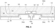
- Figures 2 and 3 illustrate alternative configurations for the package 100, according to examples. More specifically, Figure 2 illustrates a package 100(2) in which the LED 112 is coupled to the lead frame 102 via two wire bonds 116 and Figure 3 illustrates a package 100(3) in which two contacts 119 on the bottom of the LED 112 couple the LED 112 to the lead frame 102.
- Figure 2 is a cross-sectional view of a package 100(2) according to another example. The package 100(2) is similar to the package 100(1) except that in the package 100(2), the LED 112 is coupled to the lead frame 102 through two wire bonds 116 (which are coupled to the LED 112 through contacts 117) instead of through a contact 113 on the bottom of the LED 112 and a single wire bond 116.
- the fillers may adjust the physical properties of the material of molding 120 to improve the integrity and reliability of the material under application conditions of the LED device, and to achieve desired optical reflectivity for the molding 120.
- the material used for the molding 120 is durable, substantially non-yellowing, mechanically suitable, compatible with appropriate manufacturing processes, and highly reflective.
- the molding 120 has a similar coefficient of thermal expansion as the lead frame 102, where "similar" means that the coefficients of thermal expansion are within 10% of each other. Although certain possible materials for the molding 120 are listed above, any suitable material may be used.
- the lead frame including the pillars 108, comprises a conductive material.
- the conductive material may be, for example, a metal such as copper, silver, gold, nickel, palladium, combinations thereof, alloys thereof, multi-layer stacks of the same or different metals, or any other suitable material.
- An encapsulant 122 is shown disposed within the well 114.
- the encapsulant 122 comprises a transparent material that protects the LED 112 and other components within the well 144, such as the wire bond 116 if present.
- the encapsulant 122 includes materials such as wavelength converting materials, materials that improve the thermal performance of the encapsulant 122, materials that cause or reduce light scattering, materials that act as filters, or any other suitable materials.
- the LED 112 may be replaced with other types of light emitting devices such as laser diodes and semiconductor light emitting devices made from other materials systems such as other III-V materials, III-phosphide, III-arsenide, II-VI materials, ZnO, or Si-based materials may be used. Blue or UV emitting light emitting devices are often combined with one or more wavelength converting materials to produce different colors of light, such that combined light from the light emitting device and the wavelength converting materials appears white or any other color necessary for a given application.
- other types of light emitting devices such as laser diodes and semiconductor light emitting devices made from other materials systems such as other III-V materials, III-phosphide, III-arsenide, II-VI materials, ZnO, or Si-based materials may be used.
- Blue or UV emitting light emitting devices are often combined with one or more wavelength converting materials to produce different colors of light, such that combined light from the light emitting device and the wavelength converting materials appears white or any other color necessary for a given application.
- the lead frame 102 is formed.
- the posts 108 of the lead frame 102, which are exposed after forming the molding 120, are at a higher elevation than other portions of the lead frame 102, which are covered by the molding 120 when the molding 120 is formed.
- the lead frame may be formed by, for example, shaping a sheet of metal by molding, folding, stamping, punching, etching, or any other suitable technique.
- a metal layer 106 (not shown) may be formed, for example over the entire surface of lead frame 120, or only certain locations, such as on the portions of the lead frame that are exposed after forming the molding 120.
- the metal layer 106 may be formed by plating, sputtering, evaporation, or any other suitable technique.
- the molding 120 is formed on and around the lead frame 120.
- the molding 120 may be formed by, for example, molding, injection molding, transfer molding, or any other suitable technique.
- the molding 120 may be shaped to form sidewalls 118 that form a well 114 suitable for enclosing an encapsulant 122, which is formed in Figure 8 , described below.
- a majority of the bottom surface (“basin") 124 of the well 114 is covered by the molding 120, rather than the pillars 108.
- processing steps may be taken to expose areas (such as the pillars 108) that are not to be covered by the molding 120 in the final device. Suitable processing steps include wet or dry bead blasting, chemical etching, electrolysis, or any other suitable technique to clean the surface of the pillars 108. After such cleaning, other metal layers, such as silver, gold, nickel, palladium, or other suitable materials, may be deposited on the pillars 108.
- LED 112 and any other components are attached to the pillars 108 of the lead frame that are exposed. LED 112 and other components may be attached by, for example, soldering or any other suitable technique.
- an encapsulant 122 is disposed in the well 114, covering the LED 112.
- the encapsulant 122 may be formed by, for example, molding, dispensing, or any other suitable technique.
- the encapsulant 122 is disposed in the well 114 in a liquid or gel form, then cured into a solid.
- the encapsulant 122 may include wavelength converting materials to convert the light emitted by the LED chip to light of other colors. The combination of the light from the LED chip and the light emitted from the wavelength converting materials forms the final color of the light of the LED device.
- the devices illustrated in Figures 1-8 may be used in any suitable application such as, for example, general lighting, backlighting for displays, or specialized lighting applications.
- the devices described above may be incorporated into a mobile phone.
Landscapes
- Led Device Packages (AREA)
Abstract
Description
- This application claims the benefit of
U.S. Patent Application No. 15/652,603, filed on July 18, 2017 EP Patent Application No. 17184498.8, filed on August 2, 2017 - Light emitting diodes ("LEDs") are solid state devices that emit light when provided with an electrical current. LEDs are packaged in a relatively complex encasement incorporating different materials to provide various functions for the LED. One component typically used in a package is a layer of silver. The silver provides good electrical conductivity to the LED semiconductor device while also providing good optical characteristics such as high reflectivity and reflectivity of light at appropriate wavelengths. However, silver is subject to tarnishing, even when covered by an encapsulation material.
- A light emitting diode (LED) package may include a lead frame comprising a first lead frame part electrically isolated from a second lead frame part. The first lead frame part may include a first pillar that is raised above a lower surface of the first lead frame part. The second lead frame part may include a second pillar that is raised above a lower surface of the second lead frame part. A molding may cover the lower surfaces of the lead frame parts. At least a portion of the first pillar and the second pillar may remain exposed. The molding may comprise a highly optically reflective and electrically insulating material. An LED device may be disposed over only the second pillar. A first contact may be formed on the LED device. The first contact may be electrically coupled to the first pillar via a first wire bond. A second contact may be formed on the LED device. The second contact may be electrically coupled to the second pillar via a second wire bond.
- A more detailed understanding may be had from the following description, given by way of example in conjunction with the accompanying drawings, wherein like reference numerals in the figures indicate like elements, and wherein:
-
Figure 1 is a cross sectional view of an LED package, according to an example; -
Figures 2 and3 illustrate alternative configurations for the LED package, according to examples; and -
Figures 4-8 illustrate an exploded view of, and method of manufacturing, an LED package, according to an example. - Examples of different light emitting diode ("LED") implementations will be described more fully hereinafter with reference to the accompanying drawings. These examples are not mutually exclusive, and features found in one example can be combined with features found in one or more other examples to achieve additional implementations. Accordingly, it will be understood that the examples shown in the accompanying drawings are provided for illustrative purposes only and they are not intended to limit the disclosure in any way. Like numbers refer to like elements throughout.
- It will be understood that, although the terms first, second, etc. may be used herein to describe various elements, these elements should not be limited by these terms. These terms are only used to distinguish one element from another. For example, a first element could be termed a second element, and, similarly, a second element could be termed a first element, without departing from the scope of the present description. As used herein, the term "and/or" includes any and all combinations of one or more of the associated listed items.
- It will be understood that when an element such as a layer, region or substrate is referred to as being "on" or extending "onto" another element, it can be directly on or extend directly onto the other element or intervening elements may also be present. In contrast, when an element is referred to as being "directly on" or extending "directly onto" another element, there are no intervening elements present. It will also be understood that when an element is referred to as being "connected" or "coupled" to another element, it can be directly connected or coupled to the other element or intervening elements may be present. In contrast, when an element is referred to as being "directly connected" or "directly coupled" to another element, there are no intervening elements present. It will be understood that these terms are intended to encompass different orientations of the element in addition to any orientation depicted in the figures.
- Relative terms such as "below" or "above" or "upper" or "lower" or "horizontal" or "vertical" may be used herein to describe a relationship of one element, layer or region to another element, layer or region as illustrated in the figures. It will be understood that these terms are intended to encompass different orientations of the device in addition to the orientation depicted in the figures.
- A package is provided herein with physical characteristics that reduce the necessity for the use of silver, which, while having good optical qualities such as reflectivity, is susceptible to being tarnished by environmental agents. More specifically, silver has a high affinity to materials such as hydrogen sulfide, halogens, oxygen, water vapor, nitrous oxide, sulfur dioxide, and ozone, which may be found in polluted air, especially in city centers or industrial areas. These materials may result in the formation of black silver sulfide or dark yellow silver oxide (known as silver tarnish), which may significantly and rapidly reduce the reflectivity of the silver.
- The package includes a metal lead frame, a molding material disposed at least partially over the lead frame and forming a well in which light emitting diode ("LED") components are disposed, and an encapsulation material disposed within the well. The metal lead frame includes pillars on which an LED or other components are disposed and/or that serve as electrical contact points to form an electrical circuit that includes the lead frame and components within the well. Areas of the lead frame other than the pillars are covered by the molding, which is optically reflective. The top surface of the molding material within the well is flush with (or approximately flush with) the top surface of the pillars (or the top surface of any additional layers, such as a plated metal layer or the like, formed over the pillars), to form a single flush bottom surface of the well. The molding material is a highly reflective material to reflect light from the LED and provide good optical characteristics for the LED package. The lead frame configuration having raised pillars allows a more conventional material like silver to not be used in the LED package, or to be used less in the LED package, which alleviates the silver tarnishing problem. More specifically, while in conventional designs, silver would cover much of the bottom surface of the well, and thus would be subject to tarnishing, reducing the optical characteristics of the LED package, in the package of the present disclosure, the exposed surface virtually lacks silver, reflectivity being provided by the reflective molding material not subject to silver tarnishing.
-
Figure 1 is a cross sectional view of a package 100(1) according to an example. Thepackage 100 includes alead frame 102 that includes a first lead frame part 104(a) and a second lead frame part 104(b), the first lead frame part 104(a) being electrically isolated from the second lead frame part 104(b). The differentlead frame parts 104 of thelead frame 102 provide electrical coupling between components within thepackage 100 and components external to the package. For example, onelead frame part 104 may couple to one terminal of anLED device 112 and to one external wire and anotherlead frame part 104 may couple to another terminal of theLED device 112 and to a different external wire, so that theLED device 112 is integrated into a circuit. Ametal plating layer 106 is disposed over the first lead frame part 104(a) and the second lead frame part 104(b) in order to electrically couple various components, such as theLED 112, to thelead frame 102. Though in conventional designs, a plating layer is made of silver so that the plating layer can perform double duty as both electrical conductor and optical reflector, in the present disclosure, themetal plating layer 106 does not need to be silver as the reflectivity of theLED package 100 is provided by themolding material 120. Themetal plating layer 106 may be any technically feasible material other than silver, or may be silver. - The
lead frame 102 has two raised portions or "pillars" 108 that extend above alower surface 110 of thelead frame 102. Thepillars 108 serve to provide points of electrical contact for electrical components (such as the LED 112) within awell 114. Thewell 114 is formed by side-walls 118 of amolding 120 made of a molding compound. TheLED 112 is disposed on one of thepillars 108 and is electrically coupled, via awire bond 116, to apillar 108 of the second lead frame part 104(b). TheLED 112 is also electrically coupled, via an electricallyconductive contact 113, to thepillar 108 of the first lead frame part 104(a). Thepillars 108 allow electrical connections to be formed between components within thewell 114 and thelead frame 102 while minimizing the amount of exposed metal disposed, for example, over thelead frame 102. Anencapsulant 122 is disposed over the components within thewell 114 and fills the space of thewell 114. - In a conventional lead frame design, two (or more) electrically isolated parts of a lead frame are plated with a metallic material such as silver which provides both electrical coupling to the lead frame and high optical reflectivity with good color characteristics of reflected light. Silver is very often used as a particularly good electrically conductive and optically reflective material in conventional designs. However, as described above, silver is subject to tarnishing even when covered by an encapsulation material. The
lead frame 102 withpillars 108 of the present disclosure provides the function of allowing for electrical connection of components in the well 114 to thelead frame 102 while also allowing most of the bottom-most surface of the well 114 (which bottom-most surface is also called a "basin 124") to be comprised not of silver but instead of a highly optically reflective non-electrically-conductive material. Note, thebasin 124 is comprised of the top-most surfaces of themetal layer 106 and of the top-most surface of themolding 120 at the bottom of thewell 114. Although illustrated as being a flush surface, the various portions of thebasin 124 may be slightly or substantially uneven. -
Figures 2 and3 illustrate alternative configurations for thepackage 100, according to examples. More specifically,Figure 2 illustrates a package 100(2) in which theLED 112 is coupled to thelead frame 102 via twowire bonds 116 andFigure 3 illustrates a package 100(3) in which twocontacts 119 on the bottom of theLED 112 couple theLED 112 to thelead frame 102.Figure 2 is a cross-sectional view of a package 100(2) according to another example. The package 100(2) is similar to the package 100(1) except that in the package 100(2), theLED 112 is coupled to thelead frame 102 through two wire bonds 116 (which are coupled to theLED 112 through contacts 117) instead of through acontact 113 on the bottom of theLED 112 and asingle wire bond 116. TheLED 112 is mounted on to apillar 108, but has no electrical coupling to the pillar through the bottom surface of theLED 112.Figure 3 is a cross-sectional view of a package 100(3) according to yet another example. In the package 100(3), theLED 112 is coupled to thelead frame 102 through twocontacts 119 and without wire bonds 116. TheLED 112 is mounted over both illustratedlead frame parts 104 to allow the twocontacts 119 to be coupled to the twolead frame parts 104 while theLED 112 is directly over the twolead frame parts 104. - Although a specific configuration of components within the
well 114 is shown, it should be understood that various configurations not illustrated are within the teachings of the present disclosure. The composition of thebasin 124 varies depending on the shape, size, and number ofpillars 108. In various embodiments, thebasin 124 is mostly a non-conductive material, such as the material of themolding 120. In such embodiments, thebasin 124 is 50% non-conductive material, 85% non-conductive material, or 95% non-conductive material. The portion of thebasin 124 that is not the non-conductive material comprises the conductive material of thelead frame 102 and/or themetal layer 106. - In the example packages 100 illustrated above, the
molding 120 comprises a highly reflective material. For example, themolding 120 comprises a silicone molding compound with high thermal, mechanical, electrical, and photochemical stability, such as, but not limited to, thermal set poly-siloxane and its derivative compounds. In various embodiments, themolding 120 is formed from an electrically insulating material such as plastic, thermoset material, thermoplastic material, polymer, epoxy polymer resin, composite materials based on silicone, composite molding compound silicone, polycyclohexylene, polycyclohexylene terephthalate, epoxy molding compound, liquid crystal polymers, mixtures thereof, or any other suitable material. The material forming themolding 120 may include fillers such as organic or inorganic materials. The fillers may adjust the physical properties of the material ofmolding 120 to improve the integrity and reliability of the material under application conditions of the LED device, and to achieve desired optical reflectivity for themolding 120. The material used for themolding 120 is durable, substantially non-yellowing, mechanically suitable, compatible with appropriate manufacturing processes, and highly reflective. Preferably, themolding 120 has a similar coefficient of thermal expansion as thelead frame 102, where "similar" means that the coefficients of thermal expansion are within 10% of each other. Although certain possible materials for themolding 120 are listed above, any suitable material may be used. - The
metal plating layer 106 is illustrated disposed over the top surface of thelead frame 102, but in various examples, themetal plating layer 106 is disposed over only a portion of the top surface of thelead frame 102, such as over thepillars 108. Further, themetal plating layer 106 may be any electrically conductive material. In some embodiments, themetal plating 106 andmolding 120 that form thebasin 124 are both materials that are stable at high temperature, stable at high doses of short wavelength (blue and UV) light, and inert to corrosive gases such as sulfur and/or its compounds, chlorine and/or its compounds, nitrogen oxides, ozone, water vapor, oxygen, and other pollutants in the environment of the intended applications of theLED 112. Although thelead frame 102 in the example packages 100 is illustrated as having ametal layer 106 disposed over the top surface to provide compatibility forwire bond 116 ofFigures 1 and2 , orcontacts 119 inFigure 3 , as well as protection to the base metal of thelead frame 102. In some embodiments, nosuch metal layer 106 exists, for example, when such compatibility and/or protection are not required. - The lead frame, including the
pillars 108, comprises a conductive material. The conductive material may be, for example, a metal such as copper, silver, gold, nickel, palladium, combinations thereof, alloys thereof, multi-layer stacks of the same or different metals, or any other suitable material. - Although a wire bond is illustrated in some embodiments, any suitable arrangement for electrically connecting the
LED 112 to thelead frame 102 may be used. For example, metal bridge(s), solder, conductive epoxy, or other suitable connections may be used instead of a wire bond, in any of thepackages 100 illustrated. - As described above, in
Figures 1-3 , themolding 120 forms a well 114 in which various components are disposed. In other embodiments, just enough of the material forming themolding 120 is used to structurally secure the relative positions of thelead frame parts 104 without forming thewell 114. In other embodiments, themolding 120 forms the well 114 withshallow side walls 118, for example just deep enough to contain theLED 112, wire bond(s) 116 (if present) or other components within thewell 114. - An
encapsulant 122 is shown disposed within thewell 114. In some embodiments, theencapsulant 122 comprises a transparent material that protects theLED 112 and other components within the well 144, such as thewire bond 116 if present. In some embodiments, theencapsulant 122 includes materials such as wavelength converting materials, materials that improve the thermal performance of theencapsulant 122, materials that cause or reduce light scattering, materials that act as filters, or any other suitable materials. - Though an
LED 112 is described, in various embodiments, theLED 112 may be replaced with other types of light emitting devices such as laser diodes and semiconductor light emitting devices made from other materials systems such as other III-V materials, III-phosphide, III-arsenide, II-VI materials, ZnO, or Si-based materials may be used. Blue or UV emitting light emitting devices are often combined with one or more wavelength converting materials to produce different colors of light, such that combined light from the light emitting device and the wavelength converting materials appears white or any other color necessary for a given application. -
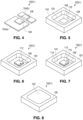
Figures 4-8 illustrate a method of forming the package 100(1) ofFigure 1 and also, together, illustrate an exploded view of the package 100(1) ofFigure 1 . It should be understood that, for clarity, some components have been omitted from the views illustrated inFigures 4-8 . For example, themetal layer 106 is not shown. - In
Figure 4 , thelead frame 102 is formed. Theposts 108 of thelead frame 102, which are exposed after forming themolding 120, are at a higher elevation than other portions of thelead frame 102, which are covered by themolding 120 when themolding 120 is formed. The lead frame may be formed by, for example, shaping a sheet of metal by molding, folding, stamping, punching, etching, or any other suitable technique. After forming thelead frame 102, a metal layer 106 (not shown) may be formed, for example over the entire surface oflead frame 120, or only certain locations, such as on the portions of the lead frame that are exposed after forming themolding 120. Themetal layer 106 may be formed by plating, sputtering, evaporation, or any other suitable technique. - In
Figure 5 , themolding 120 is formed on and around thelead frame 120. Themolding 120 may be formed by, for example, molding, injection molding, transfer molding, or any other suitable technique. Themolding 120 may be shaped to form sidewalls 118 that form a well 114 suitable for enclosing anencapsulant 122, which is formed inFigure 8 , described below. After forminginsulator 120, only portions of thelead frame 102 are exposed, such as thepillars 108. Other portions of thelead frame 120 are covered by themolding 120. A majority of the bottom surface ("basin") 124 of the well 114 is covered by themolding 120, rather than thepillars 108. After forming themolding 120, other processing steps may be taken to expose areas (such as the pillars 108) that are not to be covered by themolding 120 in the final device. Suitable processing steps include wet or dry bead blasting, chemical etching, electrolysis, or any other suitable technique to clean the surface of thepillars 108. After such cleaning, other metal layers, such as silver, gold, nickel, palladium, or other suitable materials, may be deposited on thepillars 108. - In
Figure 6 ,LED 112 and any other components, such as an electrostatic discharge protection chip or any other suitable component, are attached to thepillars 108 of the lead frame that are exposed.LED 112 and other components may be attached by, for example, soldering or any other suitable technique. - In
Figure 7 , one ormore wire bonds 116 are formed, if used. Other electrical connections in addition to or as an alternative to wirebonds 116 may be formed, to provide electrical connection betweenLED 112 and thepillars 108. - In
Figure 7 , anencapsulant 122 is disposed in the well 114, covering theLED 112. Theencapsulant 122 may be formed by, for example, molding, dispensing, or any other suitable technique. In some embodiments, theencapsulant 122 is disposed in the well 114 in a liquid or gel form, then cured into a solid. Theencapsulant 122 may include wavelength converting materials to convert the light emitted by the LED chip to light of other colors. The combination of the light from the LED chip and the light emitted from the wavelength converting materials forms the final color of the light of the LED device. - The devices illustrated in
Figures 1-8 , or any of the devices described above, may be used in any suitable application such as, for example, general lighting, backlighting for displays, or specialized lighting applications. In some embodiments, the devices described above may be incorporated into a mobile phone. - Having described the embodiments in detail, those skilled in the art will appreciate that, given the present disclosure, modifications may be made without departing from the spirit of the inventive concept described herein. In particular, different features and components of the different devices described herein may be used in any of the other devices, or features and components may be omitted from any of the devices. A characteristic of a structure described in the context of one embodiment, may be applicable to any embodiment. Therefore, it is not intended that the scope of the description be limited to the specific embodiments illustrated and described.
- Although features and elements are described above in particular combinations, one of ordinary skill in the art will appreciate that each feature or element can be used alone or in any combination with the other features and elements. In addition, the methods described herein may be implemented in a computer program, software, or firmware incorporated in a computer-readable medium for execution by a computer or processor. Examples of computer-readable media include electronic signals (transmitted over wired or wireless connections) and computer-readable storage media. Examples of computer-readable storage media include, but are not limited to, a read only memory (ROM), a random access memory (RAM), a register, cache memory, semiconductor memory devices, magnetic media such as internal hard disks and removable disks, magneto-optical media, and optical media such as CD-ROM disks, and digital versatile disks (DVDs).
-
- [Aspect 1] A light emitting diode (LED) package, comprising:
- a first portion of a lead frame, the first portion comprising a single first pillar having a first surface and sidewalls;
- a second portion of the lead frame electrically isolated from the first portion, the second portion comprising a second pillar having a second surface and sidewalls;
- a molding comprising an optically reflective and electrically insulating material on the first portion and the second portion, the molding adjacent to the sidewalls of the first pillar and the sidewalls of the second pillar;
- an LED device on the first surface;
- a first wire bond electrically coupling the LED device to the first surface; and
- a second wire bond electrically coupling the LED device to the second surface.
- [Aspect 2] The LED package of
aspect 1, wherein:
the molding comprises sidewalls shaped to form a well. - [Aspect 3] The LED package of
aspect 2, further comprising:
an encapsulant within the well, the encapsulant configured to physically protect the LED device. - [Aspect 4] The LED package of
aspect 1, wherein the first pillar has a width that is greater than a width of the LED device. - [Aspect 5] The LED package of
aspect 1, wherein the molding comprises a silicone material. - [Aspect 6] The LED package of
aspect 1, further comprising:
a plated metal layer between the lead frame and the molding and between the lead frame and the LED device. - [Aspect 7] The LED package of
aspect 1, further comprising:
a plated metal layer between the first pillar and the LED device as well as the molding and between the second pillar and the molding. - [Aspect 8] A method of forming a light emitting diode (LED) package, the method comprising:
- forming a first portion of a lead frame, the first portion comprising a single first pillar having a first surface and sidewalls;
- forming a second portion of the lead frame, the second portion electrically isolated from the first portion, the second portion comprising a second pillar having a second surface and sidewalls;
- forming a molding on the first portion and the second portion, the molding adjacent to the sidewalls of the first pillar and the sidewalls of the second pillar;
- forming an LED device on the first surface;
- forming a first wire bond electrically coupling the LED device to the first surface; and
- forming a second wire bond electrically coupling the LED device to the second surface.
- [Aspect 9] The method of aspect 8, wherein forming the molding comprises:
forming sidewalls shaped to form a well. - [Aspect 10] The method of aspect 9, further comprising:
forming an encapsulant within the well. - [Aspect 11] The method of aspect 8, wherein the first surface has a width that is greater than a width of the LED device.
- [Aspect 12] The method of aspect 8, wherein the molding comprises a silicone material.
- [Aspect 13] The method of aspect 8, further comprising:
forming a plated metal layer between the lead frame and the molding and between the lead frame and the LED device. - [Aspect 14] The method of aspect 8, further comprising:
forming a plated metal layer between the first pillar and the LED device as well as the molding and between the second pillar and the molding.
Claims (12)
- A light emitting diode (LED) package, comprising:a first portion of a lead frame, the first portion of the lead frame comprising a first pillar having a first surface that is raised above a lower surface of the first portion of the lead frame;a second portion of the lead frame electrically isolated from the first portion of the lead frame, the second portion of the lead frame comprising a second pillar having a second surface that is raised above a lower surface of the second portion of the lead frame;a molding comprising an optically reflective and electrically insulating material on the first portion of the lead frame and the second portion of the lead frame, the molding adjacent to sidewalls of the first pillar and sidewalls of the second pillar, and the molding comprising sidewalls shaped to form a well;an LED device on the first surface;a plated metal layer between the lead frame and the molding and between the lead frame and the LED device; anda further metal layer deposited on the first surface and the second surface exposed from the molding,wherein the first pillar and the second pillar are configured such that 50% or more of a surface exposed at a bottom of the well comprises a surface of the molding.
- The LED package of claim 1, further comprising:
a first wire bond electrically coupling the LED device to the first surface. - The LED package of claim 1, further comprising:
a second wire bond electrically coupling the LED device to the second surface. - The LED package of claim 1, further comprising:
an encapsulant within the well, the encapsulant configured to physically protect the LED device. - The LED package of claim 1, wherein the first pillar has a width that is greater than a width of the LED device.
- The LED package of claim 1, wherein the molding comprises a silicone material.
- A method of forming a light emitting diode (LED) package, the method comprising:forming a first portion of a lead frame, the first portion of the lead frame comprising a first pillar having a first surface that is raised above a lower surface of the first portion of the lead frame;forming a second portion of the lead frame, the second portion of the lead frame electrically isolated from the first portion of the lead frame, the second portion of the lead frame comprising a second pillar having a second surface that is raised above a lower surface of the second portion of the lead frame;forming a plated metal layer on the lead frame, including on the first surface and on the second surface;forming a molding on the first portion of the lead frame and the second portion of the lead frame, the molding adjacent to sidewalls of the first pillar and sidewalls of the second pillar, and the molding comprising sidewalls shaped to form a well;cleaning the first surface and the second surface exposed from the molding;after the cleaning, depositing a further metal layer on the first surface and the second surface; andforming an LED device on the first surface,wherein the first pillar and the second pillar are configured such that 50% or more of a surface exposed at a bottom of the well comprises a surface of the molding.
- The method of claim 7, further comprising:
electrically coupling the LED device to the first surface via a first wire bond. - The method of claim 7, further comprising:
electrically coupling the LED device to the second surface via a second wire bond. - The method of claim 7, further comprising:
forming an encapsulant within the well. - The method of claim 7, wherein the first surface has a width that is greater than a width of the LED device.
- The method of claim 7, wherein the molding comprises a silicone material.
Applications Claiming Priority (4)
| Application Number | Priority Date | Filing Date | Title |
|---|---|---|---|
| US15/652,603 US10381534B2 (en) | 2017-07-18 | 2017-07-18 | Light emitting device including a lead frame and an insulating material |
| EP17184498 | 2017-08-02 | ||
| EP18747087.7A EP3656001A1 (en) | 2017-07-18 | 2018-07-12 | Light emitting device including a lead frame and an insulating material |
| PCT/US2018/041774 WO2019018193A1 (en) | 2017-07-18 | 2018-07-12 | Light emitting device including a lead frame and an insulating material |
Related Parent Applications (1)
| Application Number | Title | Priority Date | Filing Date |
|---|---|---|---|
| EP18747087.7A Division EP3656001A1 (en) | 2017-07-18 | 2018-07-12 | Light emitting device including a lead frame and an insulating material |
Publications (2)
| Publication Number | Publication Date |
|---|---|
| EP4583672A2 true EP4583672A2 (en) | 2025-07-09 |
| EP4583672A3 EP4583672A3 (en) | 2025-09-24 |
Family
ID=63047471
Family Applications (2)
| Application Number | Title | Priority Date | Filing Date |
|---|---|---|---|
| EP18747087.7A Ceased EP3656001A1 (en) | 2017-07-18 | 2018-07-12 | Light emitting device including a lead frame and an insulating material |
| EP25169804.9A Pending EP4583672A3 (en) | 2017-07-18 | 2018-07-12 | Light emitting device including a lead frame and an insulating material cross reference to related applications |
Family Applications Before (1)
| Application Number | Title | Priority Date | Filing Date |
|---|---|---|---|
| EP18747087.7A Ceased EP3656001A1 (en) | 2017-07-18 | 2018-07-12 | Light emitting device including a lead frame and an insulating material |
Country Status (6)
| Country | Link |
|---|---|
| EP (2) | EP3656001A1 (en) |
| JP (2) | JP2020527864A (en) |
| KR (1) | KR102408302B1 (en) |
| CN (1) | CN111357124A (en) |
| TW (1) | TWI832819B (en) |
| WO (1) | WO2019018193A1 (en) |
Families Citing this family (4)
| Publication number | Priority date | Publication date | Assignee | Title |
|---|---|---|---|---|
| US11335842B2 (en) * | 2018-02-14 | 2022-05-17 | Maven Optronics Co., Ltd. | Chip-scale packaging light-emitting device with electrode polarity identifier and method of manufacturing the same |
| JP2020167366A (en) | 2019-02-26 | 2020-10-08 | ローム株式会社 | Semiconductor light emitting device and manufacturing method of semiconductor light emitting device |
| DE102020107409B4 (en) * | 2020-03-18 | 2023-11-02 | OSRAM Opto Semiconductors Gesellschaft mit beschränkter Haftung | HOUSING FOR AN OPTOELECTRONIC SEMICONDUCTOR COMPONENT AND OPTOELECTRONIC SEMICONDUCTOR COMPONENT |
| CN114628263B (en) * | 2022-05-13 | 2022-08-05 | 威海三维曲板智能装备有限公司 | Photoelectric hybrid packaging structure and manufacturing method thereof |
Family Cites Families (26)
| Publication number | Priority date | Publication date | Assignee | Title |
|---|---|---|---|---|
| US3830762A (en) * | 1973-08-24 | 1974-08-20 | Us Agriculture | Polysaccharide-containing elastomers |
| KR100867515B1 (en) * | 2004-12-06 | 2008-11-07 | 삼성전기주식회사 | Light emitting device package |
| US20070126020A1 (en) * | 2005-12-03 | 2007-06-07 | Cheng Lin | High-power LED chip packaging structure and fabrication method thereof |
| US8044418B2 (en) * | 2006-07-13 | 2011-10-25 | Cree, Inc. | Leadframe-based packages for solid state light emitting devices |
| EP2303951B1 (en) * | 2008-07-24 | 2018-03-07 | Industrias Negromex, S.a. De C.v. | Processes for making silane, hydrophobated silica, silica masterbatch and rubber products |
| US8044420B2 (en) * | 2009-01-15 | 2011-10-25 | Advanced Semiconductor Engineering, Inc. | Light emitting diode package structure |
| KR101047603B1 (en) * | 2009-03-10 | 2011-07-07 | 엘지이노텍 주식회사 | Light emitting device package and its manufacturing method |
| JP2010212508A (en) * | 2009-03-11 | 2010-09-24 | Sony Corp | Light emitting element mounting package, light emitting device, backlight, and liquid crystal display |
| JP5509878B2 (en) | 2010-01-27 | 2014-06-04 | 凸版印刷株式会社 | Manufacturing method of lead frame substrate for LED light emitting device |
| US8525213B2 (en) * | 2010-03-30 | 2013-09-03 | Lg Innotek Co., Ltd. | Light emitting device having multiple cavities and light unit having the same |
| JP5618189B2 (en) * | 2010-07-30 | 2014-11-05 | 大日本印刷株式会社 | Lead frame with resin and manufacturing method thereof, and semiconductor device and manufacturing method thereof |
| CN103392242B (en) * | 2011-02-28 | 2017-02-22 | 日亚化学工业株式会社 | Light emitting device |
| KR101303168B1 (en) * | 2011-07-26 | 2013-09-09 | 안상정 | Conneted body with semiconductor light emitting regions |
| JP5818149B2 (en) * | 2011-09-09 | 2015-11-18 | 大日本印刷株式会社 | Lead frame with resin, semiconductor device, lighting device, method for manufacturing lead frame with resin, and method for manufacturing semiconductor device |
| KR20130098048A (en) * | 2012-02-27 | 2013-09-04 | 엘지이노텍 주식회사 | Light emitting device package |
| JP2013219104A (en) | 2012-04-05 | 2013-10-24 | Toppan Printing Co Ltd | Lead frame for led and method of manufacturing the same |
| JP5788839B2 (en) * | 2012-08-03 | 2015-10-07 | 信越化学工業株式会社 | Curable resin composition, cured product thereof and optical semiconductor device using the same |
| CN104124237A (en) * | 2013-04-26 | 2014-10-29 | 光明半导体(天津)有限公司 | Light-emitting diode packaging piece and manufacturing method thereof |
| JP6176101B2 (en) * | 2013-12-17 | 2017-08-09 | 日亜化学工業株式会社 | Resin package and light emitting device |
| JP2017501577A (en) * | 2014-01-07 | 2017-01-12 | コーニンクレッカ フィリップス エヌ ヴェKoninklijke Philips N.V. | Light emitting device package |
| EP3110878A1 (en) * | 2014-02-27 | 2017-01-04 | E. I. du Pont de Nemours and Company | Micropulp-elastomer masterbatches and compounds based thereon |
| JP6262578B2 (en) * | 2014-03-18 | 2018-01-17 | スタンレー電気株式会社 | Light emitting device |
| EP3975272A1 (en) | 2014-05-29 | 2022-03-30 | Suzhou Lekin Semiconductor Co., Ltd. | Light emitting device package |
| EP3237454B1 (en) * | 2014-12-22 | 2020-08-12 | DuPont Industrial Biosciences USA, LLC | Polymeric blend containing poly alpha-1,3-glucan |
| JP6056914B2 (en) * | 2015-07-07 | 2017-01-11 | 大日本印刷株式会社 | Lead frame with resin, semiconductor device and lighting device |
| AU2017348076B2 (en) * | 2016-10-28 | 2022-02-24 | Nutrition & Biosciences USA 4, Inc. | Rubber compositions comprising polysaccharides |
-
2018
- 2018-07-12 EP EP18747087.7A patent/EP3656001A1/en not_active Ceased
- 2018-07-12 CN CN201880060567.4A patent/CN111357124A/en active Pending
- 2018-07-12 WO PCT/US2018/041774 patent/WO2019018193A1/en not_active Ceased
- 2018-07-12 JP JP2020502262A patent/JP2020527864A/en active Pending
- 2018-07-12 EP EP25169804.9A patent/EP4583672A3/en active Pending
- 2018-07-12 KR KR1020207004530A patent/KR102408302B1/en active Active
- 2018-07-18 TW TW107124773A patent/TWI832819B/en active
-
2023
- 2023-05-10 JP JP2023077765A patent/JP7605400B2/en active Active
Also Published As
| Publication number | Publication date |
|---|---|
| TWI832819B (en) | 2024-02-21 |
| EP4583672A3 (en) | 2025-09-24 |
| WO2019018193A1 (en) | 2019-01-24 |
| JP2020527864A (en) | 2020-09-10 |
| KR102408302B1 (en) | 2022-06-14 |
| CN111357124A (en) | 2020-06-30 |
| KR20200033889A (en) | 2020-03-30 |
| EP3656001A1 (en) | 2020-05-27 |
| JP7605400B2 (en) | 2024-12-24 |
| JP2023090921A (en) | 2023-06-29 |
| TW201916413A (en) | 2019-04-16 |
Similar Documents
| Publication | Publication Date | Title |
|---|---|---|
| JP7605400B2 (en) | Light emitting device including a leadframe and an insulating material - Patents.com | |
| US8525213B2 (en) | Light emitting device having multiple cavities and light unit having the same | |
| US9711702B2 (en) | Light emitting device and method of manufacturing the same | |
| KR101760545B1 (en) | Resin-attached lead frame, method for manufacturing same, and lead frame | |
| CN101315963B (en) | Semiconductor light-emitting device | |
| US9012947B2 (en) | Light emitting diode package and method of manufacturing the same | |
| EP2378571B1 (en) | Light emitting diode | |
| US10559728B2 (en) | Semiconductor package structure | |
| US20160118549A1 (en) | Light emitting device package | |
| US20060208364A1 (en) | LED device with flip chip structure | |
| US8487336B2 (en) | Light emitting device package | |
| US20030001166A1 (en) | Light-emitting diode with plastic reflector cup | |
| JP6034175B2 (en) | LED module | |
| US10381534B2 (en) | Light emitting device including a lead frame and an insulating material | |
| CN102769089B (en) | Semiconductor packaging structure | |
| US8587016B2 (en) | Light emitting device package having light emitting device on inclined side surface and lighting system including the same | |
| KR101377603B1 (en) | Side-view light emitting device package and backlight unit comprising the same | |
| TWI573299B (en) | Package module structure of compound semiconductor component and manufacturing method thereof | |
| KR101714042B1 (en) | The light- | |
| KR101293993B1 (en) | Led package and method for manufacturing the same | |
| KR101911939B1 (en) | Light emitting device | |
| US10062822B1 (en) | Light-emitting diode package structure with an improved structure, light-emitting device using the same, and method of making the same | |
| KR102136373B1 (en) | Lead frame for light emitting device package, manufacturing method thereof, and manufacturing method light emitting device package | |
| KR20150080838A (en) | Light emitting device |
Legal Events
| Date | Code | Title | Description |
|---|---|---|---|
| PUAI | Public reference made under article 153(3) epc to a published international application that has entered the european phase |
Free format text: ORIGINAL CODE: 0009012 |
|
| STAA | Information on the status of an ep patent application or granted ep patent |
Free format text: STATUS: THE APPLICATION HAS BEEN PUBLISHED |
|
| AC | Divisional application: reference to earlier application |
Ref document number: 3656001 Country of ref document: EP Kind code of ref document: P |
|
| AK | Designated contracting states |
Kind code of ref document: A2 Designated state(s): AL AT BE BG CH CY CZ DE DK EE ES FI FR GB GR HR HU IE IS IT LI LT LU LV MC MK MT NL NO PL PT RO RS SE SI SK SM TR |
|
| PUAL | Search report despatched |
Free format text: ORIGINAL CODE: 0009013 |
|
| AK | Designated contracting states |
Kind code of ref document: A3 Designated state(s): AL AT BE BG CH CY CZ DE DK EE ES FI FR GB GR HR HU IE IS IT LI LT LU LV MC MK MT NL NO PL PT RO RS SE SI SK SM TR |
|
| RIC1 | Information provided on ipc code assigned before grant |
Ipc: H10H 20/857 20250101AFI20250818BHEP Ipc: H10H 20/85 20250101ALI20250818BHEP Ipc: H10H 20/856 20250101ALN20250818BHEP |
|
| STAA | Information on the status of an ep patent application or granted ep patent |
Free format text: STATUS: REQUEST FOR EXAMINATION WAS MADE |
|
| 17P | Request for examination filed |
Effective date: 20260318 |